EP2777049B1 - Conductive paste and electronic device and solar cell including an electrode formed using the conductive paste - Google Patents
Conductive paste and electronic device and solar cell including an electrode formed using the conductive paste Download PDFInfo
- Publication number
- EP2777049B1 EP2777049B1 EP12847137.2A EP12847137A EP2777049B1 EP 2777049 B1 EP2777049 B1 EP 2777049B1 EP 12847137 A EP12847137 A EP 12847137A EP 2777049 B1 EP2777049 B1 EP 2777049B1
- Authority
- EP
- European Patent Office
- Prior art keywords
- metallic glass
- based metallic
- electrode
- conductive paste
- glass
- Prior art date
- Legal status (The legal status is an assumption and is not a legal conclusion. Google has not performed a legal analysis and makes no representation as to the accuracy of the status listed.)
- Active
Links
Images


Classifications
-
- H—ELECTRICITY
- H01—ELECTRIC ELEMENTS
- H01B—CABLES; CONDUCTORS; INSULATORS; SELECTION OF MATERIALS FOR THEIR CONDUCTIVE, INSULATING OR DIELECTRIC PROPERTIES
- H01B1/00—Conductors or conductive bodies characterised by the conductive materials; Selection of materials as conductors
- H01B1/20—Conductive material dispersed in non-conductive organic material
- H01B1/22—Conductive material dispersed in non-conductive organic material the conductive material comprising metals or alloys
-
- B—PERFORMING OPERATIONS; TRANSPORTING
- B22—CASTING; POWDER METALLURGY
- B22F—WORKING METALLIC POWDER; MANUFACTURE OF ARTICLES FROM METALLIC POWDER; MAKING METALLIC POWDER; APPARATUS OR DEVICES SPECIALLY ADAPTED FOR METALLIC POWDER
- B22F1/00—Metallic powder; Treatment of metallic powder, e.g. to facilitate working or to improve properties
- B22F1/10—Metallic powder containing lubricating or binding agents; Metallic powder containing organic material
-
- B—PERFORMING OPERATIONS; TRANSPORTING
- B23—MACHINE TOOLS; METAL-WORKING NOT OTHERWISE PROVIDED FOR
- B23K—SOLDERING OR UNSOLDERING; WELDING; CLADDING OR PLATING BY SOLDERING OR WELDING; CUTTING BY APPLYING HEAT LOCALLY, e.g. FLAME CUTTING; WORKING BY LASER BEAM
- B23K35/00—Rods, electrodes, materials, or media, for use in soldering, welding, or cutting
- B23K35/02—Rods, electrodes, materials, or media, for use in soldering, welding, or cutting characterised by mechanical features, e.g. shape
- B23K35/0222—Rods, electrodes, materials, or media, for use in soldering, welding, or cutting characterised by mechanical features, e.g. shape for use in soldering or brazing
- B23K35/0244—Powders, particles or spheres; Preforms made therefrom
- B23K35/025—Pastes, creams or slurries
-
- B—PERFORMING OPERATIONS; TRANSPORTING
- B23—MACHINE TOOLS; METAL-WORKING NOT OTHERWISE PROVIDED FOR
- B23K—SOLDERING OR UNSOLDERING; WELDING; CLADDING OR PLATING BY SOLDERING OR WELDING; CUTTING BY APPLYING HEAT LOCALLY, e.g. FLAME CUTTING; WORKING BY LASER BEAM
- B23K35/00—Rods, electrodes, materials, or media, for use in soldering, welding, or cutting
- B23K35/02—Rods, electrodes, materials, or media, for use in soldering, welding, or cutting characterised by mechanical features, e.g. shape
- B23K35/0255—Rods, electrodes, materials, or media, for use in soldering, welding, or cutting characterised by mechanical features, e.g. shape for use in welding
- B23K35/0261—Rods, electrodes or wires
-
- B—PERFORMING OPERATIONS; TRANSPORTING
- B23—MACHINE TOOLS; METAL-WORKING NOT OTHERWISE PROVIDED FOR
- B23K—SOLDERING OR UNSOLDERING; WELDING; CLADDING OR PLATING BY SOLDERING OR WELDING; CUTTING BY APPLYING HEAT LOCALLY, e.g. FLAME CUTTING; WORKING BY LASER BEAM
- B23K35/00—Rods, electrodes, materials, or media, for use in soldering, welding, or cutting
- B23K35/22—Rods, electrodes, materials, or media, for use in soldering, welding, or cutting characterised by the composition or nature of the material
- B23K35/24—Selection of soldering or welding materials proper
- B23K35/28—Selection of soldering or welding materials proper with the principal constituent melting at less than 950°C
- B23K35/286—Al as the principal constituent
-
- B—PERFORMING OPERATIONS; TRANSPORTING
- B23—MACHINE TOOLS; METAL-WORKING NOT OTHERWISE PROVIDED FOR
- B23K—SOLDERING OR UNSOLDERING; WELDING; CLADDING OR PLATING BY SOLDERING OR WELDING; CUTTING BY APPLYING HEAT LOCALLY, e.g. FLAME CUTTING; WORKING BY LASER BEAM
- B23K35/00—Rods, electrodes, materials, or media, for use in soldering, welding, or cutting
- B23K35/22—Rods, electrodes, materials, or media, for use in soldering, welding, or cutting characterised by the composition or nature of the material
- B23K35/24—Selection of soldering or welding materials proper
- B23K35/30—Selection of soldering or welding materials proper with the principal constituent melting at less than 1550°C
- B23K35/3006—Ag as the principal constituent
-
- B—PERFORMING OPERATIONS; TRANSPORTING
- B23—MACHINE TOOLS; METAL-WORKING NOT OTHERWISE PROVIDED FOR
- B23K—SOLDERING OR UNSOLDERING; WELDING; CLADDING OR PLATING BY SOLDERING OR WELDING; CUTTING BY APPLYING HEAT LOCALLY, e.g. FLAME CUTTING; WORKING BY LASER BEAM
- B23K35/00—Rods, electrodes, materials, or media, for use in soldering, welding, or cutting
- B23K35/22—Rods, electrodes, materials, or media, for use in soldering, welding, or cutting characterised by the composition or nature of the material
- B23K35/24—Selection of soldering or welding materials proper
- B23K35/30—Selection of soldering or welding materials proper with the principal constituent melting at less than 1550°C
- B23K35/302—Cu as the principal constituent
-
- B—PERFORMING OPERATIONS; TRANSPORTING
- B23—MACHINE TOOLS; METAL-WORKING NOT OTHERWISE PROVIDED FOR
- B23K—SOLDERING OR UNSOLDERING; WELDING; CLADDING OR PLATING BY SOLDERING OR WELDING; CUTTING BY APPLYING HEAT LOCALLY, e.g. FLAME CUTTING; WORKING BY LASER BEAM
- B23K35/00—Rods, electrodes, materials, or media, for use in soldering, welding, or cutting
- B23K35/22—Rods, electrodes, materials, or media, for use in soldering, welding, or cutting characterised by the composition or nature of the material
- B23K35/24—Selection of soldering or welding materials proper
- B23K35/30—Selection of soldering or welding materials proper with the principal constituent melting at less than 1550°C
- B23K35/3033—Ni as the principal constituent
-
- C—CHEMISTRY; METALLURGY
- C22—METALLURGY; FERROUS OR NON-FERROUS ALLOYS; TREATMENT OF ALLOYS OR NON-FERROUS METALS
- C22C—ALLOYS
- C22C21/00—Alloys based on aluminium
-
- C—CHEMISTRY; METALLURGY
- C22—METALLURGY; FERROUS OR NON-FERROUS ALLOYS; TREATMENT OF ALLOYS OR NON-FERROUS METALS
- C22C—ALLOYS
- C22C45/00—Amorphous alloys
-
- C—CHEMISTRY; METALLURGY
- C22—METALLURGY; FERROUS OR NON-FERROUS ALLOYS; TREATMENT OF ALLOYS OR NON-FERROUS METALS
- C22C—ALLOYS
- C22C45/00—Amorphous alloys
- C22C45/08—Amorphous alloys with aluminium as the major constituent
-
- H—ELECTRICITY
- H01—ELECTRIC ELEMENTS
- H01B—CABLES; CONDUCTORS; INSULATORS; SELECTION OF MATERIALS FOR THEIR CONDUCTIVE, INSULATING OR DIELECTRIC PROPERTIES
- H01B1/00—Conductors or conductive bodies characterised by the conductive materials; Selection of materials as conductors
- H01B1/02—Conductors or conductive bodies characterised by the conductive materials; Selection of materials as conductors mainly consisting of metals or alloys
-
- H—ELECTRICITY
- H10—SEMICONDUCTOR DEVICES; ELECTRIC SOLID-STATE DEVICES NOT OTHERWISE PROVIDED FOR
- H10F—INORGANIC SEMICONDUCTOR DEVICES SENSITIVE TO INFRARED RADIATION, LIGHT, ELECTROMAGNETIC RADIATION OF SHORTER WAVELENGTH OR CORPUSCULAR RADIATION
- H10F10/00—Individual photovoltaic cells, e.g. solar cells
- H10F10/10—Individual photovoltaic cells, e.g. solar cells having potential barriers
- H10F10/14—Photovoltaic cells having only PN homojunction potential barriers
- H10F10/146—Back-junction photovoltaic cells, e.g. having interdigitated base-emitter regions on the back side
-
- H—ELECTRICITY
- H10—SEMICONDUCTOR DEVICES; ELECTRIC SOLID-STATE DEVICES NOT OTHERWISE PROVIDED FOR
- H10F—INORGANIC SEMICONDUCTOR DEVICES SENSITIVE TO INFRARED RADIATION, LIGHT, ELECTROMAGNETIC RADIATION OF SHORTER WAVELENGTH OR CORPUSCULAR RADIATION
- H10F71/00—Manufacture or treatment of devices covered by this subclass
-
- H—ELECTRICITY
- H10—SEMICONDUCTOR DEVICES; ELECTRIC SOLID-STATE DEVICES NOT OTHERWISE PROVIDED FOR
- H10F—INORGANIC SEMICONDUCTOR DEVICES SENSITIVE TO INFRARED RADIATION, LIGHT, ELECTROMAGNETIC RADIATION OF SHORTER WAVELENGTH OR CORPUSCULAR RADIATION
- H10F77/00—Constructional details of devices covered by this subclass
- H10F77/20—Electrodes
- H10F77/206—Electrodes for devices having potential barriers
- H10F77/211—Electrodes for devices having potential barriers for photovoltaic cells
-
- B—PERFORMING OPERATIONS; TRANSPORTING
- B22—CASTING; POWDER METALLURGY
- B22F—WORKING METALLIC POWDER; MANUFACTURE OF ARTICLES FROM METALLIC POWDER; MAKING METALLIC POWDER; APPARATUS OR DEVICES SPECIALLY ADAPTED FOR METALLIC POWDER
- B22F3/00—Manufacture of workpieces or articles from metallic powder characterised by the manner of compacting or sintering; Apparatus specially adapted therefor ; Presses and furnaces
- B22F3/10—Sintering only
-
- Y—GENERAL TAGGING OF NEW TECHNOLOGICAL DEVELOPMENTS; GENERAL TAGGING OF CROSS-SECTIONAL TECHNOLOGIES SPANNING OVER SEVERAL SECTIONS OF THE IPC; TECHNICAL SUBJECTS COVERED BY FORMER USPC CROSS-REFERENCE ART COLLECTIONS [XRACs] AND DIGESTS
- Y02—TECHNOLOGIES OR APPLICATIONS FOR MITIGATION OR ADAPTATION AGAINST CLIMATE CHANGE
- Y02E—REDUCTION OF GREENHOUSE GAS [GHG] EMISSIONS, RELATED TO ENERGY GENERATION, TRANSMISSION OR DISTRIBUTION
- Y02E10/00—Energy generation through renewable energy sources
- Y02E10/50—Photovoltaic [PV] energy
- Y02E10/547—Monocrystalline silicon PV cells
Definitions
- Example embodiments relate to a conductive paste, and an electronic device and/or a solar cell including at least one electrode formed using the conductive paste.
- a solar cell is a photoelectric conversion device that transforms light (e.g., solar energy) into electrical energy.
- Solar cells have attracted much attention as a potentially infinite and pollution-free next generation energy source.
- a solar cell may include p-type and n-type semiconductors.
- EHP electron-hole pair
- the solar cell produces electrical energy by transferring electrons and holes to the n-type and p-type semiconductors, respectively, and then collecting the electrons and holes in electrodes.
- a solar cell desirably has as high efficiency as possible for producing electrical energy from solar energy.
- the solar cell desirably produces as many electron-hole pairs as possible and then collects the produced charges without loss as well as desirably absorbs light with less loss.
- An electrode for a solar cell may be fabricated using a deposition method.
- Some deposition methods may be complicated, may have a high cost, and/or may take a relatively long time. Accordingly, a simpler method, e.g., screen-printing a conductive paste including a conductive material, has been suggested.
- Document EP2325848 discloses a conductive paste including a conductive powder including a plurality of conductive particles, a metallic glass disposed between adjacent conductive particles of the conductive powder, and an organic vehicle in which the conductive powder and metallic glass are disposed is provided, wherein the metallic glass may include an alloy of copper (Cu), zirconium (Zr), nickel (Ni), iron (Fe), titanium (Ti), magnesium (Mg), or a combination thereof.
- the conductive paste when an electrode is fabricated by using a conductive paste, the conductive paste generally may need to be fired at a relatively high temperature of about 900 °C. The firing at a higher temperature may deteriorate a passivation layer disposed beneath or on the electrode, and thus deteriorate efficiency.
- the electronic device according to the invention has lower resistivity and contact resistance.
- spatially relative terms such as “beneath,” “below,” “lower,” “above,” “upper” and the like, may be used herein for ease of description to describe one element or feature's relationship to another element(s) or feature(s) as illustrated in the figures. It will be understood that the spatially relative terms are intended to encompass different orientations of the device in use or operation in addition to the orientation depicted in the figures. For example, if the device in the figures is turned over, elements described as “below” or “beneath” other elements or features would then be oriented “above” the other elements or features. Thus, the exemplary term “below” can encompass both an orientation of above and below. The device may be otherwise oriented (rotated 90 degrees or at other orientations) and the spatially relative descriptors used herein interpreted accordingly.
- Example embodiments are described herein with reference to cross-sectional illustrations that are schematic illustrations of idealized embodiments (and intermediate structures) of example embodiments. As such, variations from the shapes of the illustrations as a result, for example, of manufacturing techniques and/or tolerances, are to be expected. Thus, example embodiments are not to be construed as limited to the particular shapes of regions illustrated herein but are to include deviations in shapes that result, for example, from manufacturing. For example, an implanted region illustrated as a rectangle may have rounded or curved features and/or a gradient of implant concentration at its edges rather than a binary change from implanted to non-implanted region.
- a buried region formed by implantation may result in some implantation in the region between the buried region and the surface through which the implantation takes place.
- the regions illustrated in the figures are schematic in nature and their shapes are not intended to illustrate the actual shape of a region of a device and are not intended to limit the scope of example embodiments.
- element refers to a metal and a semimetal.
- a conductive paste according to the invention includes a conductive powder, a metallic glass, and an organic vehicle.
- the conductive powder is a silver (Ag)-containing metal (e.g., silver or a silver alloy), an aluminum (Al)-containing metal (e.g., aluminum or an aluminum alloy), a copper (Cu)-containing metal (e.g., copper (Cu) or a copper alloy), a nickel (Ni)-containing metal (e.g., nickel (Ni) or a nickel alloy).
- a silver (Ag)-containing metal e.g., silver or a silver alloy
- Al aluminum
- Cu copper
- Cu copper
- Ni nickel-containing metal
- Ni nickel (Ni) or a nickel alloy
- the conductive powder may have a size (e.g., an average largest particle size) ranging from about 0.1 nanometers (nm) to about 50 micrometers ( ⁇ m).
- the conductive powder may be particles having a substantially spherical shape. However, example embodiments are not limited thereto and the conductive powder may alternatively be a non-spherical shape (e.g., flakes).
- the conductive powder is included in an amount of about 30 to about 99 wt%, based on the total amount of the conductive paste.
- the metallic glass may be an alloy of greater than or equal to two kinds of metals and/or semi-metals at least partly having an amorphous portion, and may be called an amorphous metal.
- the amorphous portion may be about 50 to 100 wt% of the metallic glass, for example, about 70 to 100 wt%, or about 90 to 100 wt%.
- the metallic glass has relatively low resistivity and a relatively high conductivity, unlike conventional glass (e.g., silicate).
- the metallic glass may be formed to include an amorphous structure by heating the metallic glass above its melting temperature (T m ) and then using a rapid quenching process to cool the metallic glass. Rapid quenching processes are well known in the art so a detailed description of a rapid quenching process is omitted herein.
- the metallic glass has a glass transition temperature of less than or equal to 350 °C and has a supercooled liquid region of greater than or equal to 0 K.
- the supercooled liquid region of the metallic glass may be between about 0 K to about 200 K, about 0 K to about 100 K, and/or about 6 K to about 90 K.
- the metallic glass may be plastically deformed at a glass transition temperature and show a liquid-like behavior.
- the liquid-like behavior may be maintained in a supercooled liquid region between a glass transition temperature (Tg) and a crystalline temperature (T c ).
- the metallic glass when the metallic glass shows a liquid-like behavior, the metallic glass may show wettability against a lower layer and thus enlarge a contact area between the conductive paste and the lower layer.
- an electrode for a solar cell formed by applying a conductive paste on a semiconductor substrate according to example embodiments is illustrated referring to FIGS. 1 to 4 .
- FIGS. 1 to 3 are schematic diagrams showing a process in which a conductive paste according to example embodiments is applied on a semiconductor substrate and then heated and transformed by the heat
- FIG. 4 shows a schematic diagram enlarging the region 'A' shown in FIG. 3 .
- a conductive paste including a conductive powder 120a and a metallic glass 115a is applied on a semiconductor substrate 110.
- the conductive powder 120a and the metallic glass 115a respectively may be a particle type, respectively.
- the metallic glass 115a when the conductive paste is heated up to higher than or equal to a glass transition temperature (Tg) of the metallic glass 115a, the metallic glass 115a may soften and change into a liquid-like metallic glass 115b.
- Tg glass transition temperature
- the liquid-like metallic glass 115b has wettability on the semiconductor substrate 110 and thus may contact a larger area of the semiconductor substrate 110.
- the conductive powder 120a when the conductive paste is heated up to higher than or equal to a sintering temperature of a conductive powder 120a, the conductive powder 120a combines to form a conductive powder chunk 120b.
- a portion of the conductive powder 120a is diffused into the liquid-like metallic glass 115b and forms a solid solution therewith.
- a desired (and/or alternatively predetermined) buffer portion 117 may be formed between the conductive powder chunk 120b and the semiconductor substrate 110.
- the buffer portion 117 may include a conductive powder component 120c and a metallic glass component 115c.
- the process shown in FIGS. 2 to 4 may occur at higher than or equal to the glass transition temperature of a metallic glass.
- the conductive paste may have wettability, and form a solid solution and a buffer portion, as aforementioned.
- the conductive paste may be generally fired in a furnace at a process temperature of greater than or equal to about 900 °C when applied to form an electrode.
- the firing at a higher temperature may deteriorate a passivation layer or an organic layer for a flexible electronic device, deteriorating efficiency.
- the conductive paste includes a metallic glass having a glass transition temperature of less than or equal to 350 °C and a supercooled liquid region of greater than or equal to 0 K, and thus may have a sufficient contact area with a lower layer due to the aforementioned wettability, forming of a solid solution and a buffer portion, although fired at a temperature of lower than or equal to 600 °C. Accordingly, the conductive paste may not only secure conductivity of an electrode but also reduce (and/or prevent) degradation of a passivation layer and/or an organic material in a device, and thus reduce (and/or prevent) efficiency deterioration of the device.
- the supercooled liquid region of 0 K refers to a case in which a metallic glass partly has a crystal phase, and thus, no clear glass transition temperature.
- the metallic glass having a glass transition temperature of less than or equal to 350 °C and a supercooled liquid region of greater than or equal to 0 K includes an aluminum-based metallic glass, a cerium-based metallic glass, a strontium-based metallic glass, a gold-based metallic glass, an ytterbium metallic glass, a zinc-based metallic glass, a platinum-based metallic glass, and a palladium-based metallic.
- the aluminum-based metallic glass, cerium-based metallic glass, strontium-based metallic glass, gold-based metallic glass, ytterbium metallic glass, zinc-based metallic glass, platinum-based metallic glass, and palladium-based metallic glass has a glass transition temperature of less than or equal to 350 °C.
- the metallic glass may have a glass transition temperature from 10 to 350 °C.
- the aluminum-based metallic glass, cerium-based metallic glass, strontium-based metallic glass, gold-based metallic glass, ytterbium metallic glass, zinc-based metallic glass, platinum-based metallic glass, and palladium-based metallic glass is alloy including each of aluminum, cerium, strontium, gold, ytterbium, zinc, platinum, and palladium as a main component, respectively, and further including at least one selected from nickel (Ni), yttrium (Y), cobalt (Co), lanthanum (La), zirconium (Zr), iron (Fe), titanium (Ti), calcium (Ca), beryllium (Be), magnesium (Mg), sodium (Na), molybdenum (Mo), tungsten (W), tin (Sn), zinc (Zn), potassium (K), lithium (Li), phosphorus (P), palladium (Pd), platinum (Pt), rubidium (Rb), chromium (Cr), strontium (Sr), cerium (Ce), p
- the aluminum-based metallic glass may be an alloy containing aluminum and at least one of nickel (Ni), yttrium (Y), cobalt (Co), lanthanum (La), zirconium (Zr), iron (Fe), titanium (Ti), and calcium (Ca).
- the cerium-based metallic glass may be an alloy containing cerium and at least one of aluminum (Al), copper (Cu), and niobium (Nb).
- the strontium-based metallic glass may be an alloy containing strontium and at least one of magnesium (Mg), lithium (Li), zinc (Zn), and copper (Cu).
- the gold-based metallic glass may be an alloy containing gold and at least one of copper (Cu), silicon (Si), silver (Ag), and palladium (Pd).
- the ytterbium metallic glass may be an alloy containing ytterbium and at least one of zinc (Zn), magnesium (Mg), copper (Cu), and calcium (Ca); silver (Ag), and mercury (Hg).
- the zinc-based metallic glass may be an alloy containing zinc and at least one of strontium (Sr), ytterbium (Yb), magnesium (Mg), copper (Cu), and calcium (Ca), and lithium (Li).
- the platinum-based metallic glass may be an alloy containing platinum and at least one of nickel (Ni), copper (Cu), and phosphorus (P).
- the palladium-based metallic glass may be an alloy containing palladium and at least one of nickel (Ni), copper (Cu), and phosphorus (P).
- the aluminum-based metallic glass may contain about 84 at% to about 90 at% aluminum (Al) inclusive, and may further contain at least one of nickel (Ni), cobalt (Co), and iron (Fe), and at least one of yttrium (Y), lanthanum (La), and zirconium (Zr).
- the cesium-based metallic glass may be represented by the chemical formula Ce 70-a Cu 20 Al 10 Nb a where a is about 0 at% to about 2 at% inclusive.
- the strontium-based metallic glass may be represented by the formula Sr 60-x Yb x Mg 20-y Li y Zn 20-z Cu z , where x is about 0 at% to about 20 at% inclusive, y is about 0 at% to about 11 at% inclusive, and z is about 0 at% to about 5 at% inclusive.
- the gold-based metallic glass may contain about 50 at% to about 70 at % gold (Au) inclusive, and may further contain copper (Cu), and at least one of silicon (Si), silver (Ag), and palladium (Pd),
- the ytterbium-based glass may contains about 60 at% to about 70 at% yterrbium (Yb) inclusive, and may further contain about 15 at% to about 20 at% zinc (Zn) inclusive, and a balance including at least one of magnesium (Mg) and copper (Cu).
- the zinc-based metallic glass may be represented by the chemical formula Zn 40 Mg 11 Ca 35-n Yb n where n is about 0 at% to about 4 at% inclusive.
- the platinum-based metallic glass may be Pt 57.5 Cu 14.7 Ni 5.3 P 22.5 and Pt 60 Ni 15 P 25 .
- the aluminum-based metallic glass may be selected from the group consisting of Al 86 Ni 8 Y 6 , Al 84.5 Ni 5.5 Y 10 , Al 89 Co 6 La 5 , Al 89.5 Co 3.5 Y 7 , Al 88 Co 4 Y 8 , AL 86.5 Co 4.5 Y 9 , Al 85 Co 5 Y 10 , Al 90 Fe 5 La 5 , Al 88 Fe 5 Y 7 , Al 88 Ni 8 La 4 , Al 88 Ni 7 La 5 , Al 86 Ni 9 La 4 , Al 87 Ni 8 La 5 , Al 86 Ni 9 La 5 , Al 86 Ni 8 La 6 , Al 85 Ni 10 La 5 , Al 84 Ni 11 La 5 , A 184 Ni 10 La 6 , AL 87.5 Fe 5 Y 7 Ti 0.5 , AL 87 Fe 5 Y 7 Ti 1 , Al 86 Fe 5 Y 7 Ti 2 , Al 85 Ni 5 Y 8 Co 2 , Al 86 Ni 8 Y 4.5 La 1.5 , Al 85 Ni 5 Y 10 Y
- the strontium-based metallic glass is selected from the group consisting of Sr 60 Mg 18 Zn 22 , Sr 60 Li 11 Mg 9 Zn 20 , Sr 60 Li 5 Mg 15 Zn 20 , Sr 60 Mg 20 Zn 15 Cu 5 , and Sr 40 Yb 20 Mg 20 Zn 15 Cu 5 .
- the gold-based metallic glass may be selected from the group consisting of Au 50 Cu 33 Si 17 , Au 50 Cu 25.5 Ag 7.5 Si 17 , Au 60 Cu 15.5 Ag 7.5 Si 17 , Au 65 Cu 10.5 Ag 7.5 Si 17 , Au 70 Cu 5.5 Ag 7.5 Si 17 , and Au 49 Cu 26.9 Ag 5.5 Pd 2.3 Si 16.3 .
- the zinc-based metallic glass may be selected from the group consisting of Zn 40 Mg 11 Ca 31 Yb 18 , and Zn 40 Mg 11 Ca 35 Yb 14 .
- the platinum-based metallic glass may be selected from the group consisting of Pt 57.5 Cu 14.7 Ni 5.3 P 22.5 and Pt 60 Ni 15 P 25 .
- the palladium-based metallic glass may be Pd 43 Ni 10 Cu 27 P 20 .
- Table 1 shows glass transition temperatures, crystalline temperatures, and supercooled liquid regions of aluminum-based metallic glasses that may be used in conductive pastes according to example embodiments.
- Table 2 shows glass transition temperatures, crystalline temperatures, and supercooled liquid regions of the cerium-based metallic glass, strontium-based metallic glass, gold-based metallic glass, ytterbium metallic glass, zinc-based metallic glass, calcium-based metallic glass, magnesium-based metallic glass, platinum-based metallic glass, and palladium-based metallic glass.
- the calcium-based metallic glass examples and the magnesium-based metallic glass example in table 2 represent examples not falling under the present invention.
- Table 3 shows glass transition temperatures, crystalline temperatures, and supercooled liquid regions of zirconium-based metallic glass.
- the zirconium-based metallic glass examples in table 3 do not form part of the present invention.
- the metallic glass is included in an amount of about 0.1 to about 20 wt% based on the total amount of the conductive paste.
- the conductive paste may further include a glass frit and/or crystalline powder including the same element as at least one element of the metallic glass, as an additive.
- the organic vehicle may include an organic compound to impart viscosity to the conductive paste when mixed with the conductive powder, metallic glass and the additive, and a solvent capable of dissolving the conductive powder, the metallic glass, and the organic compound.
- the organic compound may include, for example, at least one selected from a (meth)acrylate, a cellulose, e.g., ethyl cellulose, a phenol, an alcohol, tetrafluoroethylene (e.g., TEFLON, a tetrafluoroethylene compound marked by Dupont Corporation), or a combination thereof, and may further include an additive, e.g., a surfactant, a thickener, a stabilizer, or a combination thereof.
- a surfactant e.g., a surfactant, a thickener, a stabilizer, or a combination thereof.
- the solvent may be any solvent that is capable of dissolving or suspending the above compounds and may include, for example, at least one selected from terpineol, butylcarbitol, butylcarbitol acetate, pentanediol, dipentyne, limonene, ethylene glycol alkylether, diethylene glycol alkylether, ethylene glycol alkylether acetate diethylene glycol alkylether acetate, diethylene glycol dialkylether acetate, triethylene glycol alkylether acetate, triethylene glycol alkylether, propylene glycol alkylether, propylene glycol phenylether, dipropylene glycol alkylether, tripropylene glycol alkylether, propylene glycol alkylether acetate, dipropylene glycol alkylether acetate, tripropylene glycol alkyl acetate, dimethylphthalic acid, diethylphthalic acid, dibutyl
- the organic vehicle is included in a balance amount except for the solid components.
- the conductive paste may be prepared by screen printing and firing, and may be used for manufacturing an electrode for an electronic device.
- the electrode for an electronic device may include a sintered product of the conductive paste.
- the sintered product of the conductive paste may not have a glass transition temperature (Tg), different from the conductive paste and a sintered product of a glass frit.
- the electrode may have contact resistance of less than or equal to about 1 kQm2.
- the electrode may have contact resistance ranging from about 1 ⁇ cm2 to about 20 mQm2.
- the electrode may have resistivity less than or equal to about 10 m ⁇ m. When the electrode has resistivity within the range, the electrode may effectively bring about less power loss and effectively improve efficiency of an electronic device, for example, a solar cell.
- the electrode may have resistivity ranging from about 1 ⁇ cm to about 15 ⁇ cm.
- FIG. 5 is a cross-sectional view showing a solar cell according to example embodiments.
- a solar energy incident side of the semiconductor substrate 110 is termed a front side and the opposite side is called a rear side, although alternative configurations are possible.
- a solar cell may include a semiconductor substrate 110 doped with a p-type or n-type impurity.
- the semiconductor substrate 110 may include a semiconductor, for example crystalline silicon or a compound semiconductor.
- the crystalline silicon may be, for example, a silicon wafer.
- the p-type impurity may be a Group III element, e.g., boron (B), and the n-type impurity may be a Group V element, e.g., phosphorus (P).
- the front surface of the semiconductor substrate 110 may be surface textured.
- the surface textured semiconductor substrate 110 may have protrusions and depressions, e.g., a pyramid shape or a porous structure, e.g., a honeycomb shape.
- the surface textured semiconductor substrate 110 may increase the surface area to increase the light absorption rate and reduce reflectance, thereby improving solar cell efficiency.
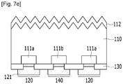
- the semiconductor substrate 110 may include a first doping region 111a and a second doping region 111b on the rear side of the semiconductor substrate 110.
- the first doping region 111a may be doped with an n-type impurity
- the second doping region 111b may be doped with a p-type impurity.
- the first doping region 111a and the second doping region 111b may be alternately disposed on the rear side of the semiconductor substrate 110.
- the insulation layer 112 is formed on the semiconductor substrate 110.
- the insulation layer 112 may be formed of a material that absorbs less light and has an insulating property, for example, silicon nitride (SiN x ), silicon oxide (SiO 2 ), titanium oxide (TiO 2 ), aluminum oxide (Al 2 O 3 ), magnesium oxide (MgO), cerium oxide (CeO 2 ), and a combination thereof, and may be formed of a single layer or multiple layers.
- the insulation layer 112 may have a thickness of about 200 to 1500 ⁇ .
- the insulation layer 112 may be an anti-reflective coating (ARC) that decreases the reflectivity of light and increases selectivity of a particular wavelength region on the surface of the solar cell, and simultaneously improves properties of silicon on the surface of the semiconductor substrate 110, thereby increasing efficiency of the solar cell.
- ARC anti-reflective coating
- a passivation layer 130 including a plurality of contact holes may be disposed on the rear side of the semiconductor substrate 110.
- the passivation layer 130 may be made of silicon oxide, silicon nitride, and/or aluminum oxide.
- a first electrode 120 electrically connected to the first doping region 111a and a second electrode 140 electrically connected to the second doping region 111b are respectively formed.
- the first electrode 120 may contact the first doping region 111a through contact holes of the passivation layer 130, while the second electrode 140 may contact the second doping region 111b through contact holes of the passivation layer 130.
- the first electrode 120 and the second electrode 140 may be alternately disposed.
- the first electrode 120 may include a first buffer portion 115a in a region contacting a first doping region 111a and a first electrode portion 121 in the regions other than the first buffer portion 115a.
- the second electrode 140 may include a second buffer portion 115b in a region contacting a second doping region 111b and a second electrode portion 141 in the regions other than the second buffer portion 115b.
- the first electrode 120 and the second electrode 140 may be formed of the aforementioned conductive paste.
- the first and second electrodes 120 and 140 are not limited thereto, and either of the first electrode 120 and the second electrode 140 may be formed of the aforementioned conductive paste.
- the first buffer portion 115a and the second buffer portion 115b may be formed from a softened metallic glass of the conductive paste and are thus conductive.
- the first buffer portion 115a may respectively contact the first doping region 111a and the first electrode portion 121, and thus enlarge the area of a path through which charges move from the first doping region 111a to the first electrode portion 121 and prevent or reduce loss of the charges.
- the second buffer portion 115b may respectively contact the second doping region 111b and the second electrode portion 141, and thus enlarge the area of a path through which charges move from the second doping region 111b to the second electrode portion 141 and prevent or reduce loss of the charges.
- a solar cell may include both of the first electrode 120 and the second electrode 140 on the rear side, and thus has a smaller area for a metal on the front side, decreasing light absorption loss and improving efficiency.
- a semiconductor substrate 110 doped with, for example, an n-type impurity is prepared.
- the semiconductor substrate 110 may be surface-textured, and an insulation layer 112 and passivation layer 130a may be disposed on the front and rear sides of the semiconductor substrate 110, respectively.
- the insulation layer 112 and the passivation layer 130a may be provided by chemical vapor deposition (CVD), for example.
- the passivation layer 130a may be patterned into a passivation layer 130 that exposes portions on the rear side of the semiconductor substrate 110.
- the first doping region 111a and the second doping region 111b may be formed by sequentially doping a p-type impurity and an n-type impurity at a relatively high concentration on portions of the rear side of the semiconductor substrate 110 that are exposed by the passivation layer 130a.
- the first doping region 111a and the second doping region 111b may each have a higher impurity concentration than an impurity concentration of the substrate 110.
- the first doping region 111a and the second doping region 111b may be formed in the rear side of the semiconductor substrate 110 prior to forming the passivation layer 130/130a on the rear side of the semiconductor substrate.
- a lithography pattern may be formed to expose portions of the substrate 110, and impurities may be subsequently implanted into the exposed portions of the substrate 110 in order to form the first doping region 11a and the second doping region 111b, respectively.
- a conductive paste 120a for forming at least one first electrode is applied on a portion of the passivation layer 130 corresponding to the first doping region 111a
- a conductive paste 140a for forming at least one second electrode is applied on a portion of the passivation layer 130 corresponding to the second doping region 111b.
- the conductive paste 120a for the forming first electrode and the conductive paste 140b for forming the second electrode may be disposed by a screen printing method.
- the conductive paste 120a for forming the first electrode may be one of the above-described conductive pastes according to example embodiments and the conductive paste 140a for forming the second electrode may be one of the above-described conductive pastes according to example embodiments, described with reference to FIGS. 1-4 and Tables 1-2.
- a composition of a conductive paste 120a used to form the first electrode may be the same as or different than a composition of a conductive paste 140a used to form the second electrode.
- the metallic glass, conductive powder, and/or organic vehicle in a conductive paste 120a to form the first electrode may the same as or different than the metallic glass, conductive powder, and/or organic vehicle of a conductive paste 140a used to form the second electrode.
- the conductive paste 120a for forming the first electrode and the conductive paste 120b for forming the second electrode may be fired together or separately.
- the firing may be performed in a furnace at a furnace process temperature of lower than or equal to 600 °C (and/or a temperature of lower than or equal to 350 °C).
- a passivation layer 130 may have defects. Defects in the passivation layer may remarkably deteriorate the efficiency of a solar cell.
- the first electrode 120 and the second electrode 140 structures may be formed on the rear surface of the semiconductor substrate 110 after the conductive pastes 120a and 140a described in FIG. 7D are fired.
- a conductive paste according to the invention includes a metallic glass having a glass transition temperature of less than or equal to 350 °C, and when the conductive paste is heated at a lower temperature than 600 °C, the metallic glass becomes liquid-like. Accordingly, the conductive paste may be sufficiently wet against a semiconductor substrate.
- the conductive paste may be applied to an electrode for a solar cell, but not limited thereto, and may be applied to form an electrode for other electronic devices such as a light-emitting device, an organic-based device, and the like.
- the conductive paste may be used to form an electrode at the temperature of lower than or equal to about 600 °C, and thus, may be efficiently applied to a flexible electronic device including a plurality of organic layers.
- FIGS. 5 and 7A to 7E describe a solar cell and a method of manufacturing a solar cell having first and second electrodes 120 and 140 on a rear side of the solar cell, example embodiments are not limited thereto.
- the electrodes of one of more solar cells according to example embodiments may be electrically connected in series, parallel, and/or series-parallel with the electrodes of one or more solar cells according to example embodiments to form a solar cell module.
- Silver (Ag) powder and metallic glass Al 84.5 Ni 5.5 Y 10 are added to an organic vehicle including an ethylcellulose binder, a surfactant, and a butylcarbitol/butylcarbitol acetate solvent.
- the silver (Ag) powder, the metallic glass Al 84.5 Ni 5.5 Y 10 , and the organic vehicle are respectively mixed in an amount of 82.58 wt%, 3.93 wt%, and 13.49 wt% based on the total amount of the conductive paste.
- the mixture is kneaded with a 3-roll mill, preparing a conductive paste.
- the conductive paste is coated on a silicon wafer 110 by a screen printing method.
- the coated conductive paste is heated to about 600 °C using a belt furnace.
- the heated conductive paste is cooled down, fabricating an electrode sample.
- An electrode sample is fabricated by preparing a conductive paste according to the same method as the example, except for using glass frit having a glass transition temperature of less than or equal to about 450 °C instead of the metallic glass Al 84.5 Ni 5.5 Y 10 .
- An electrode sample is fabricated by preparing a conductive paste according to the same method as the example, except for using Ni 60 Nb 30 Ta 10 having a glass transition temperature of about 650 °C instead of the metallic glass Al 84.5 Ni 5.5 Y 10 .
- the electrode sample according to the example is examined using a transmission electron microscope (TEM).
- TEM transmission electron microscope
- FIG. 6 is the transmission electron microscope (TEM) photograph of the electrode according to the example.
- a buffer portion 115a, 115b is formed between a silicon wafer 111a, 111b and an electrode portion 121, 141 including silver (Ag) as a main component.
- the buffer portion 115a includes both silver (Ag) and aluminum (Al), which is identified through energy dispersive X-ray spectroscopy (EDS) of a transmission electron microscope (TEM).
- the conductivity is calculated by using resistivity and contact resistance.
- the resistivity is calculated by measuring the electrode cross-section with a laser confocal microscope after measuring line resistance with a 2-point probe.
- the contact resistance is calculated by a transmission line method (TLM).
- the electrode according to the example has lower resistivity and contact resistance than the one according to the comparative examples.
- the electrode according to the example is fired at a relatively low temperature of about 600 °C but has sufficiently low resistivity and contact resistance and improved resistivity and contact resistance compared with the electrode fabricated by using a conductive paste including glass frit.
- the electrode according to Comparative Example 2 is not fabricated at a relatively low temperature of about 600 °C, and thus was not measured regarding conductivity.
Landscapes
- Engineering & Computer Science (AREA)
- Mechanical Engineering (AREA)
- Chemical & Material Sciences (AREA)
- Materials Engineering (AREA)
- Metallurgy (AREA)
- Organic Chemistry (AREA)
- Spectroscopy & Molecular Physics (AREA)
- Dispersion Chemistry (AREA)
- Physics & Mathematics (AREA)
- Conductive Materials (AREA)
- Photovoltaic Devices (AREA)
- Manufacturing & Machinery (AREA)
- Life Sciences & Earth Sciences (AREA)
- Sustainable Development (AREA)
- Sustainable Energy (AREA)
- Compositions Of Macromolecular Compounds (AREA)
- Electrodes Of Semiconductors (AREA)
Description
- Example embodiments relate to a conductive paste, and an electronic device and/or a solar cell including at least one electrode formed using the conductive paste.
- A solar cell is a photoelectric conversion device that transforms light (e.g., solar energy) into electrical energy. Solar cells have attracted much attention as a potentially infinite and pollution-free next generation energy source.
- A solar cell may include p-type and n-type semiconductors. When an electron-hole pair ("EHP") is produced by light absorbed in a photoactive layer of the semiconductors, the solar cell produces electrical energy by transferring electrons and holes to the n-type and p-type semiconductors, respectively, and then collecting the electrons and holes in electrodes.
- A solar cell desirably has as high efficiency as possible for producing electrical energy from solar energy. In order to improve this efficiency, the solar cell desirably produces as many electron-hole pairs as possible and then collects the produced charges without loss as well as desirably absorbs light with less loss.
- An electrode for a solar cell may be fabricated using a deposition method. Some deposition methods may be complicated, may have a high cost, and/or may take a relatively long time. Accordingly, a simpler method, e.g., screen-printing a conductive paste including a conductive material, has been suggested.
- Document
EP2325848 discloses a conductive paste including a conductive powder including a plurality of conductive particles, a metallic glass disposed between adjacent conductive particles of the conductive powder, and an organic vehicle in which the conductive powder and metallic glass are disposed is provided, wherein the metallic glass may include an alloy of copper (Cu), zirconium (Zr), nickel (Ni), iron (Fe), titanium (Ti), magnesium (Mg), or a combination thereof. - However, when an electrode is fabricated by using a conductive paste, the conductive paste generally may need to be fired at a relatively high temperature of about 900 °C. The firing at a higher temperature may deteriorate a passivation layer disposed beneath or on the electrode, and thus deteriorate efficiency.
- The present invention is defined by the independent claims. Advantageous embodiments are described in dependent claims.
- The electronic device according to the invention has lower resistivity and contact resistance.
- The foregoing and other features and advantages of example embodiments will be apparent from the more particular description of non-limiting embodiments, as illustrated in the accompanying drawings in which like reference characters refer to the same parts throughout the different views. The drawings are not necessarily to scale, emphasis instead being placed upon illustrating principles of example embodiments. In the drawings:
-
FIGS. 1 to 4 are schematic diagrams showing a process in which a conductive paste according to example embodiments is applied on a semiconductor substrate, and then heated and transformed by the heat; -
FIG. 5 is a cross-sectional view showing a solar cell according to example embodiments; -
FIG. 6 is a transmission electron microscope (TEM) photograph showing an electrode according to an example; and -
FIGS. 7A to 7E are cross-section views showing a method of fabricating a solar cell according to example embodiments. - Example embodiments will hereinafter be described in further detail with reference to the accompanying drawings, in which various embodiments are shown. This disclosure may, however, be embodied in many different forms and should not be construed as limited to the embodiments set forth herein; rather, these example embodiments are provided so that this disclosure will be thorough and complete, and will fully convey the scope of example embodiments to those of ordinary skill in the art. In the drawings, the thickness of layers, films, panels, regions, etc., are exaggerated for clarity. Like reference numerals designate like elements throughout the specification, and thus their description may be omitted.
- It will be understood that when an element is referred to as being "connected" or "coupled" to another element, it can be directly connected or coupled to the other element or intervening elements may be present. In contrast, when an element is referred to as being "directly connected" or "directly coupled" to another element, there are no intervening elements present. As used herein the term "and/or" includes any and all combinations of one or more of the associated listed items. Other words used to describe the relationship between elements or layers should be interpreted in a like fashion (e.g., "between" versus "directly between," "adjacent" versus "directly adjacent," "on" versus "directly on")..It will be understood that, although the terms "first", "second", etc. may be used herein to describe various elements, components, regions, layers and/or sections, these elements, components, regions, layers and/or sections are not to be limited by these terms. These terms are only used to distinguish one element, component, region, laver or section from another element, component, region, laver or section. Thus, a first element, component, region, laver or section discussed below could be termed a second element, component, region, laver or section without departing from the teachings of example embodiments.
- Spatially relative terms, such as "beneath," "below," "lower," "above," "upper" and the like, may be used herein for ease of description to describe one element or feature's relationship to another element(s) or feature(s) as illustrated in the figures. It will be understood that the spatially relative terms are intended to encompass different orientations of the device in use or operation in addition to the orientation depicted in the figures. For example, if the device in the figures is turned over, elements described as "below" or "beneath" other elements or features would then be oriented "above" the other elements or features. Thus, the exemplary term "below" can encompass both an orientation of above and below. The device may be otherwise oriented (rotated 90 degrees or at other orientations) and the spatially relative descriptors used herein interpreted accordingly.
- The terminology used herein is for the purpose of describing particular embodiments only and is not intended to be limiting of example embodiments. As used herein, the singular forms "a," "an" and "the" are intended to include the plural forms as well, unless the context clearly indicates otherwise. It will be further understood that the terms "comprises", "comprising", "includes" and/or "including," if used herein, specify the presence of stated features, integers, steps, operations, elements and/or components, but do not preclude the presence or addition of one or more other features, integers, steps, operations, elements, components and/or groups thereof. Expressions such as "at least one of," when preceding a list of elements, modify the entire list of elements and do not modify the individual elements of the list.
- Example embodiments are described herein with reference to cross-sectional illustrations that are schematic illustrations of idealized embodiments (and intermediate structures) of example embodiments. As such, variations from the shapes of the illustrations as a result, for example, of manufacturing techniques and/or tolerances, are to be expected. Thus, example embodiments are not to be construed as limited to the particular shapes of regions illustrated herein but are to include deviations in shapes that result, for example, from manufacturing. For example, an implanted region illustrated as a rectangle may have rounded or curved features and/or a gradient of implant concentration at its edges rather than a binary change from implanted to non-implanted region. Likewise, a buried region formed by implantation may result in some implantation in the region between the buried region and the surface through which the implantation takes place. Thus, the regions illustrated in the figures are schematic in nature and their shapes are not intended to illustrate the actual shape of a region of a device and are not intended to limit the scope of example embodiments.
- Unless otherwise defined, all terms (including technical and scientific terms) used herein have the same meaning as commonly understood by one of ordinary skill in the art to which example embodiments belong. It will be further understood that terms, such as those defined in commonly-used dictionaries, is to be interpreted as having a meaning that is consistent with their meaning in the context of the relevant art and will not be interpreted in an idealized or overly formal sense unless expressly so defined herein.
- Hereinafter, the term "element" refers to a metal and a semimetal.
- A conductive paste according to the invention includes a conductive powder, a metallic glass, and an organic vehicle.
- The conductive powder is a silver (Ag)-containing metal (e.g., silver or a silver alloy), an aluminum (Al)-containing metal (e.g., aluminum or an aluminum alloy), a copper (Cu)-containing metal (e.g., copper (Cu) or a copper alloy), a nickel (Ni)-containing metal (e.g., nickel (Ni) or a nickel alloy).
- The conductive powder may have a size (e.g., an average largest particle size) ranging from about 0.1 nanometers (nm) to about 50 micrometers (µm). The conductive powder may be particles having a substantially spherical shape. However, example embodiments are not limited thereto and the conductive powder may alternatively be a non-spherical shape (e.g., flakes).
- The conductive powder is included in an amount of about 30 to about 99 wt%, based on the total amount of the conductive paste.
- The metallic glass may be an alloy of greater than or equal to two kinds of metals and/or semi-metals at least partly having an amorphous portion, and may be called an amorphous metal. Herein, the amorphous portion may be about 50 to 100 wt% of the metallic glass, for example, about 70 to 100 wt%, or about 90 to 100 wt%. The metallic glass has relatively low resistivity and a relatively high conductivity, unlike conventional glass (e.g., silicate). The metallic glass may be formed to include an amorphous structure by heating the metallic glass above its melting temperature (Tm) and then using a rapid quenching process to cool the metallic glass. Rapid quenching processes are well known in the art so a detailed description of a rapid quenching process is omitted herein.
- The metallic glass has a glass transition temperature of less than or equal to 350 °C and has a supercooled liquid region of greater than or equal to 0 K. For example, in example embodiments, the supercooled liquid region of the metallic glass may be between about 0 K to about 200 K, about 0 K to about 100 K, and/or about 6 K to about 90 K.
- The metallic glass may be plastically deformed at a glass transition temperature and show a liquid-like behavior. The liquid-like behavior may be maintained in a supercooled liquid region between a glass transition temperature (Tg) and a crystalline temperature (Tc).
- In example embodiments, when the metallic glass shows a liquid-like behavior, the metallic glass may show wettability against a lower layer and thus enlarge a contact area between the conductive paste and the lower layer.
- For example, an electrode for a solar cell formed by applying a conductive paste on a semiconductor substrate according to example embodiments is illustrated referring to
FIGS. 1 to 4 . -
FIGS. 1 to 3 are schematic diagrams showing a process in which a conductive paste according to example embodiments is applied on a semiconductor substrate and then heated and transformed by the heat, andFIG. 4 shows a schematic diagram enlarging the region 'A' shown inFIG. 3 . - Referring to
FIG. 1 , a conductive paste including aconductive powder 120a and ametallic glass 115a is applied on asemiconductor substrate 110. Herein, theconductive powder 120a and themetallic glass 115a respectively may be a particle type, respectively. - Referring to
FIG. 2 , when the conductive paste is heated up to higher than or equal to a glass transition temperature (Tg) of themetallic glass 115a, themetallic glass 115a may soften and change into a liquid-likemetallic glass 115b. The liquid-likemetallic glass 115b has wettability on thesemiconductor substrate 110 and thus may contact a larger area of thesemiconductor substrate 110. - Referring to
FIGS. 3 and 4 , when the conductive paste is heated up to higher than or equal to a sintering temperature of aconductive powder 120a, theconductive powder 120a combines to form aconductive powder chunk 120b. - Herein, a portion of the
conductive powder 120a is diffused into the liquid-likemetallic glass 115b and forms a solid solution therewith. - Accordingly, as shown in
FIG 4 , a desired (and/or alternatively predetermined)buffer portion 117 may be formed between theconductive powder chunk 120b and thesemiconductor substrate 110. Thebuffer portion 117 may include aconductive powder component 120c and ametallic glass component 115c. - Herein, the process shown in
FIGS. 2 to 4 may occur at higher than or equal to the glass transition temperature of a metallic glass. Thus, when the glass transition temperature of a metallic glass is lower than a temperature of processing a conductive paste, the conductive paste may have wettability, and form a solid solution and a buffer portion, as aforementioned. - The conductive paste may be generally fired in a furnace at a process temperature of greater than or equal to about 900 °C when applied to form an electrode. However, the firing at a higher temperature may deteriorate a passivation layer or an organic layer for a flexible electronic device, deteriorating efficiency.
- According to the invention the conductive paste includes a metallic glass having a glass transition temperature of less than or equal to 350 °C and a supercooled liquid region of greater than or equal to 0 K, and thus may have a sufficient contact area with a lower layer due to the aforementioned wettability, forming of a solid solution and a buffer portion, although fired at a temperature of lower than or equal to 600 °C. Accordingly, the conductive paste may not only secure conductivity of an electrode but also reduce (and/or prevent) degradation of a passivation layer and/or an organic material in a device, and thus reduce (and/or prevent) efficiency deterioration of the device. Herein, the supercooled liquid region of 0 K refers to a case in which a metallic glass partly has a crystal phase, and thus, no clear glass transition temperature.
- The metallic glass having a glass transition temperature of less than or equal to 350 °C and a supercooled liquid region of greater than or equal to 0 K includes an aluminum-based metallic glass, a cerium-based metallic glass, a strontium-based metallic glass, a gold-based metallic glass, an ytterbium metallic glass, a zinc-based metallic glass, a platinum-based metallic glass, and a palladium-based metallic.
- The aluminum-based metallic glass, cerium-based metallic glass, strontium-based metallic glass, gold-based metallic glass, ytterbium metallic glass, zinc-based metallic glass, platinum-based metallic glass, and palladium-based metallic glass has a glass transition temperature of less than or equal to 350 °C. The metallic glass may have a glass transition temperature from 10 to 350 °C.
- The aluminum-based metallic glass, cerium-based metallic glass, strontium-based metallic glass, gold-based metallic glass, ytterbium metallic glass, zinc-based metallic glass, platinum-based metallic glass, and palladium-based metallic glass is alloy including each of aluminum, cerium, strontium, gold, ytterbium, zinc, platinum, and palladium as a main component, respectively, and further including at least one selected from nickel (Ni), yttrium (Y), cobalt (Co), lanthanum (La), zirconium (Zr), iron (Fe), titanium (Ti), calcium (Ca), beryllium (Be), magnesium (Mg), sodium (Na), molybdenum (Mo), tungsten (W), tin (Sn), zinc (Zn), potassium (K), lithium (Li), phosphorus (P), palladium (Pd), platinum (Pt), rubidium (Rb), chromium (Cr), strontium (Sr), cerium (Ce), praseodymium (Pr), promethium (Pm), samarium (Sm), lutetium (Lu), neodymium (Nd), niobium (Nb), gadolinium (Gd), terbium (Tb), dysprosium (Dy), holmium (Ho), erbium (Er), thulium (Tm), thorium (Th), scandium (Sc), barium (Ba), ytterbium (Yb), europium (Eu), hafnium (Hf), arsenic (As), plutonium (Pu), gallium (Ga), germanium (Ge), antimony (Sb), silicon (Si), cadmium (Cd), indium (In), platinum (Pt), manganese (Mn), niobium (Nb), osmium (Os), vanadium (V), aluminum (Al), copper (Cu), silver (Ag), and mercury (Hg). Herein, the main component refers to a component having the highest mole ratio among the components of the metallic glass.
- In example embodiments, the aluminum-based metallic glass may be an alloy containing aluminum and at least one of nickel (Ni), yttrium (Y), cobalt (Co), lanthanum (La), zirconium (Zr), iron (Fe), titanium (Ti), and calcium (Ca). In example embodiments, the cerium-based metallic glass may be an alloy containing cerium and at least one of aluminum (Al), copper (Cu), and niobium (Nb). In example embodiments, the strontium-based metallic glass may be an alloy containing strontium and at least one of magnesium (Mg), lithium (Li), zinc (Zn), and copper (Cu). In example embodiments, the gold-based metallic glass may be an alloy containing gold and at least one of copper (Cu), silicon (Si), silver (Ag), and palladium (Pd). In example embodiments, the ytterbium metallic glass may be an alloy containing ytterbium and at least one of zinc (Zn), magnesium (Mg), copper (Cu), and calcium (Ca); silver (Ag), and mercury (Hg). In example embodiments, the zinc-based metallic glass may be an alloy containing zinc and at least one of strontium (Sr), ytterbium (Yb), magnesium (Mg), copper (Cu), and calcium (Ca), and lithium (Li). In example embodiments, the platinum-based metallic glass may be an alloy containing platinum and at least one of nickel (Ni), copper (Cu), and phosphorus (P). In example embodiments, the palladium-based metallic glass may be an alloy containing palladium and at least one of nickel (Ni), copper (Cu), and phosphorus (P).
- In example embodiments, the aluminum-based metallic glass may contain about 84 at% to about 90 at% aluminum (Al) inclusive, and may further contain at least one of nickel (Ni), cobalt (Co), and iron (Fe), and at least one of yttrium (Y), lanthanum (La), and zirconium (Zr). In example embodiments, the cesium-based metallic glass may be represented by the chemical formula Ce70-aCu20Al10Nba where a is about 0 at% to about 2 at% inclusive. In example embodiments, the strontium-based metallic glass may be represented by the formula Sr60-xYbxMg20-yLiyZn20-zCuz, where x is about 0 at% to about 20 at% inclusive, y is about 0 at% to about 11 at% inclusive, and z is about 0 at% to about 5 at% inclusive. The gold-based metallic glass may contain about 50 at% to about 70 at % gold (Au) inclusive, and may further contain copper (Cu), and at least one of silicon (Si), silver (Ag), and palladium (Pd), In example embodiments, the ytterbium-based glass may contains about 60 at% to about 70 at% yterrbium (Yb) inclusive, and may further contain about 15 at% to about 20 at% zinc (Zn) inclusive, and a balance including at least one of magnesium (Mg) and copper (Cu). In example embodiments, the zinc-based metallic glass may be represented by the chemical formula Zn40Mg11Ca35-nYbn where n is about 0 at% to about 4 at% inclusive. In example embodiments, the platinum-based metallic glass may be Pt57.5 Cu14.7Ni5.3P22.5 and Pt60Ni15P25.
- In example embodiments, the aluminum-based metallic glass may be selected from the group consisting of Al86Ni8Y6, Al84.5Ni5.5Y10, Al89Co6La5, Al89.5Co3.5Y7, Al88Co4Y8, AL86.5Co4.5Y9, Al85Co5Y10, Al90Fe5La5, Al88Fe5Y7, Al88Ni8La4, Al88Ni7La5, Al86Ni9La4, Al 87Ni8La5, Al86Ni9La5, Al86Ni8La6, Al85Ni10La5, Al84Ni11La5, A184Ni10La6, AL87.5Fe5Y7Ti0.5, AL87Fe5Y7Ti1, Al86Fe5Y7Ti2, Al85Ni5Y8Co2, Al86Ni8Y4.5La1.5, Al85Ni5Y8Co2, Al86Ni6Y4.5Co 2La1.5, Al86Ni7Y5Co1La1, Al86Ni7Y4.5Co1La1.5, Al87Ni10Zr3,Al86Ni10Zr4, Al86Ni9Zr5, Al85Ni 10Zr5, Al82Zr5Ni13, and (Al86Ni9La5)98Zr2. In example embodiments, the strontium-based metallic glass is selected from the group consisting of Sr60Mg18Zn22, Sr60Li11Mg9Zn20, Sr60Li5Mg15Zn20, Sr60Mg20Zn15Cu5, and Sr40Yb20Mg20Zn15Cu5. In example embodiments, the gold-based metallic glass may be selected from the group consisting of Au50Cu33Si 17, Au50Cu25.5Ag7.5Si17, Au60Cu15.5Ag7.5Si17, Au65Cu10.5Ag7.5Si17, Au70Cu5.5Ag7.5Si17, and Au49Cu26.9Ag5.5Pd2.3Si16.3. In example embodiments, the zinc-based metallic glass may be selected from the group consisting of Zn40Mg11Ca31Yb18, and Zn40Mg11Ca35Yb14. In example embodiments, the platinum-based metallic glass may be selected from the group consisting of Pt57.5Cu 14.7Ni5.3P22.5 and Pt60Ni15P25. In example embodiments, the palladium-based metallic glass may be Pd43Ni10Cu27P20.
- Table 1 shows glass transition temperatures, crystalline temperatures, and supercooled liquid regions of aluminum-based metallic glasses that may be used in conductive pastes according to example embodiments.
-
[Table 1] Metallic glass Tg(°C) Tc(°C) ΔTx(K) Metallic glass Tg(°C) Tc(°C) ΔTx(K) Al86Ni8Y6 225 225 0 Al88La4Ni8 183 183 0 Al86Ni6Y4.5Co2La1.5 232 240 8 Al88La5Ni7 206 206 0 Al86Ni7Y5Co1La1 227 233 6 Al87La4Ni9 205 205 0 Al86Ni7Y 4.5Co1La 1.5 231 246 15 Al87La5Ni8 220 220 0 Al87Ni10Zr3 179 179 0 Al86La5Ni9 234 249 15 Al86Ni10Zr4 235 235 0 Al86La6Ni8 245 259 14 Al86Ni9Zr5 216 216 0 Al85La6Ni9 256 272 16 Al85Ni10Zr5 242 242 0 Al85La5Ni10 243 260 17 Al87.5Y7Fe5Ti0.5 275 310 35 Al84La5Ni11 265 282 17 Al87Y7Fe5Ti1 270 340 70 Al84La6Ni10 273 289 16 Al86Y7Fe5Ti2 280 350 70 Al84.5Ni5.5Y10 207 244 37 Al88Y7Fe5 258 280 22 Al85Y8Ni5Co2 267 297 30 Al89.5Co3.5Y7 187 187 0 Al84La6Ni10 273 289 16 Al88Co4Y8 234 234 0 Al89Co6La5 248 248 0 Al86.5Co4.5Y9 270 290 20 Al90Fe5La5 235 235 0 Al85Co5Y10 314 314 0 Al82Zr5Ni13 283 283 0 Al86Y4.5Ni8La1.5 234 245 11 (AL86Ni9La5)98Zr2 259 272 13 - Table 2 shows glass transition temperatures, crystalline temperatures, and supercooled liquid regions of the cerium-based metallic glass, strontium-based metallic glass, gold-based metallic glass, ytterbium metallic glass, zinc-based metallic glass, calcium-based metallic glass, magnesium-based metallic glass, platinum-based metallic glass, and palladium-based metallic glass. The calcium-based metallic glass examples and the magnesium-based metallic glass example in table 2 represent examples not falling under the present invention.
-
[Table 2] Metallic glass Tg(°C) Tc(°C) ΔTx(K) Metallic glass Tg(°C) Tc( °C) ΔTx(K) Ce70Al10Cu20 68 128 60 Yb64Zn20Mg15Cu1 84 129 45 Ce68Al10Cu20Nb2 68 149 81 Au49Cu26.9Ag5.5Pd2.3Si16.3 128 186 58 Sr60Mg18Zn22 58 101 43 Yb70Zn20Mg10 74 113 39 Sr60Li11Mg9Zn20 26 50 24 Yb62.5Zn20Mg17.5 94 125 31 Sr60Li5Mg15Zn20 42 63 21 Yb64Zn20Mg15Cu1 84 129 45 Sr60Mg20Zn15Cu5 62 101 39 Yb65Zn20Mg10Cu5 111 146 35 Sr40Yb20Mg20Zn15Cu5 63 105 42 Yb62.5Zn15Mg17.5Cu5 108 128 20 Au50Cu33Si17 110 132 22 Zn40Mg11Ca31Yb18 123 148 25 Au50Cu25.5Ag7.5Si17 104 146 42 Zn40Mg11Ca35Yb14 120 147 27 Au60Cu15.5Ag7.5Si17 86 130 44 Ca65Mg15Zn20 102 137 35 Au65Cu10.5Ag7.5Si17 69 119 50 Ca65Li9.96Mg8.54Zn16.5 44 66 22 Au70Cu5.5Ag7.5Si17 66 102 36 Mg65Cu25Y10 155 219 64 Ca65Li9.96Mg8.54Zn1 6.5 44 66 22 Pt57.5Cu14.7Ni5.3P22.5 236 325 89 Ce70Cu20Al10 68 135 67 Pt60Ni15P25 215 277 62 Pd43Ni10Cu27P20 302 392 90 - Table 3 shows glass transition temperatures, crystalline temperatures, and supercooled liquid regions of zirconium-based metallic glass. The zirconium-based metallic glass examples in table 3 do not form part of the present invention.
-
[Table 3] Metallic glass Tg(°C) Tc(°C) ΔTx(K) Metallic glass Tg(°C) Tc(°C ) ΔTx(K) Zr35Ti30Be30Cu5 301.9 452.3 150.4 Zr30Ti30Be32Cu8 318.2 463.0 144. 8 Zr35Ti30Be27.5Cu7.5 301.6 466.7 165.1 Zr30Ti30Be30Cu10 323.0 467.4 144. 4 Zr35Ti30Be26.75Cu8.25 305.2 464.2 159 Zr35Ti25Be32Cu8 323.5 462.4 138. 9 Zr54Ti11Be22.5Cu12.5 308 448 140 Zr35Ti25Be30Cu10 322 473.1 151. 1 Zr54Ti11Be17.5Cu17.5 311 449 138 Zr35Ti25Be28Cu12 323.3 471 147. 7 Zr51Ti9Be27.5Cu12.5 322 458 136 Zr40Ti20Be26.25C13.75 316.5 467.8 151. 3 Zr51Ti9Be25Cu15 319 457 138 Zr35Ti30Be33Co2 311.3 448 136. 7 Zr40Ti25Be29Cu6 306.7 455.1 148.4 Zr35Ti30Be31Co4 315.7 467.4 151. 7 Zr40Ti25Be27Cu8 306.4 464.5 158.1 Zr35Ti30Be29Co6 324.3 476.4 152. 1 Zr40Ti25Be25Cu10 306.4 470.2 163.8 Zr35Ti30Be33Fe2 313.0 449.8 136. 8 Zr27.5Ti35Be29.5Cu8 317.9 455.6 137.7 Zr35Ti30Be31Fe4 318.7 464.8 146. 1 Zr32.5Ti30Be31.5Cu6 317.4 466.7 149.3 Zr35Ti30Cu7.5Be27.5 302.0 467.0 165. 0 Zr32.5Ti30Be29.5Cu8 314.7 472.1 157.4 Zr41.2Ti13.8Ni10Cu12.5Be22.5 350.0 439.0 89.0 Zr32.5Ti30Be27.5Cu10 314.8 474.4 159.6 Zr37.5Ti25Be27.5Cu10 311.0 471.1 160.1 - The metallic glass is included in an amount of about 0.1 to about 20 wt% based on the total amount of the conductive paste.
- The conductive paste may further include a glass frit and/or crystalline powder including the same element as at least one element of the metallic glass, as an additive.
- The organic vehicle may include an organic compound to impart viscosity to the conductive paste when mixed with the conductive powder, metallic glass and the additive, and a solvent capable of dissolving the conductive powder, the metallic glass, and the organic compound.
- The organic compound may include, for example, at least one selected from a (meth)acrylate, a cellulose, e.g., ethyl cellulose, a phenol, an alcohol, tetrafluoroethylene (e.g., TEFLON, a tetrafluoroethylene compound marked by Dupont Corporation), or a combination thereof, and may further include an additive, e.g., a surfactant, a thickener, a stabilizer, or a combination thereof.
- The solvent may be any solvent that is capable of dissolving or suspending the above compounds and may include, for example, at least one selected from terpineol, butylcarbitol, butylcarbitol acetate, pentanediol, dipentyne, limonene, ethylene glycol alkylether, diethylene glycol alkylether, ethylene glycol alkylether acetate diethylene glycol alkylether acetate, diethylene glycol dialkylether acetate, triethylene glycol alkylether acetate, triethylene glycol alkylether, propylene glycol alkylether, propylene glycol phenylether, dipropylene glycol alkylether, tripropylene glycol alkylether, propylene glycol alkylether acetate, dipropylene glycol alkylether acetate, tripropylene glycol alkyl ether acetate, dimethylphthalic acid, diethylphthalic acid, dibutylphthalic acid, or desalted water.
- The organic vehicle is included in a balance amount except for the solid components.
- The conductive paste may be prepared by screen printing and firing, and may be used for manufacturing an electrode for an electronic device.
- The electrode for an electronic device may include a sintered product of the conductive paste. The sintered product of the conductive paste may not have a glass transition temperature (Tg), different from the conductive paste and a sintered product of a glass frit.
- The electrode may have contact resistance of less than or equal to about 1 kQm2. When the electrode has contact resistance within the range, power loss may be effectively decreased due to the electrode and efficiency of an electronic device, for example, a solar cell may be effectively improved. For example, the electrode may have contact resistance ranging from about 1 µΩcm2 to about 20 mQm2.
- The electrode may have resistivity less than or equal to about 10 mΩm. When the electrode has resistivity within the range, the electrode may effectively bring about less power loss and effectively improve efficiency of an electronic device, for example, a solar cell. For example, the electrode may have resistivity ranging from about 1Ωcm to about 15 µΩcm.
- An example of the electronic device is a solar cell.
FIG. 5 is a cross-sectional view showing a solar cell according to example embodiments. - Hereinafter, the spatial relationship of components will be described with respect to a
semiconductor substrate 110 for better understanding and ease of description, but the present disclosure is not limited thereto. In addition, a solar energy incident side of thesemiconductor substrate 110 is termed a front side and the opposite side is called a rear side, although alternative configurations are possible. - Referring to
FIG. 5 , a solar cell according to example embodiments may include asemiconductor substrate 110 doped with a p-type or n-type impurity. - The
semiconductor substrate 110 may include a semiconductor, for example crystalline silicon or a compound semiconductor. The crystalline silicon may be, for example, a silicon wafer. The p-type impurity may be a Group III element, e.g., boron (B), and the n-type impurity may be a Group V element, e.g., phosphorus (P). - The front surface of the
semiconductor substrate 110 may be surface textured. The surfacetextured semiconductor substrate 110 may have protrusions and depressions, e.g., a pyramid shape or a porous structure, e.g., a honeycomb shape. The surfacetextured semiconductor substrate 110 may increase the surface area to increase the light absorption rate and reduce reflectance, thereby improving solar cell efficiency. - The
semiconductor substrate 110 may include afirst doping region 111a and asecond doping region 111b on the rear side of thesemiconductor substrate 110. For example, thefirst doping region 111a may be doped with an n-type impurity, and thesecond doping region 111b may be doped with a p-type impurity. Thefirst doping region 111a and thesecond doping region 111b may be alternately disposed on the rear side of thesemiconductor substrate 110. - An
insulation layer 112 is formed on thesemiconductor substrate 110. Theinsulation layer 112 may be formed of a material that absorbs less light and has an insulating property, for example, silicon nitride (SiNx), silicon oxide (SiO2), titanium oxide (TiO2 ), aluminum oxide (Al2O3), magnesium oxide (MgO), cerium oxide (CeO2), and a combination thereof, and may be formed of a single layer or multiple layers. Theinsulation layer 112 may have a thickness of about 200 to 1500 Å. - The
insulation layer 112 may be an anti-reflective coating (ARC) that decreases the reflectivity of light and increases selectivity of a particular wavelength region on the surface of the solar cell, and simultaneously improves properties of silicon on the surface of thesemiconductor substrate 110, thereby increasing efficiency of the solar cell. - A
passivation layer 130 including a plurality of contact holes may be disposed on the rear side of thesemiconductor substrate 110. Thepassivation layer 130 may be made of silicon oxide, silicon nitride, and/or aluminum oxide. - On the rear side of the
semiconductor substrate 110, afirst electrode 120 electrically connected to thefirst doping region 111a and asecond electrode 140 electrically connected to thesecond doping region 111b are respectively formed. Thefirst electrode 120 may contact thefirst doping region 111a through contact holes of thepassivation layer 130, while thesecond electrode 140 may contact thesecond doping region 111b through contact holes of thepassivation layer 130. Thefirst electrode 120 and thesecond electrode 140 may be alternately disposed. - The
first electrode 120 may include afirst buffer portion 115a in a region contacting afirst doping region 111a and afirst electrode portion 121 in the regions other than thefirst buffer portion 115a. Thesecond electrode 140 may include asecond buffer portion 115b in a region contacting asecond doping region 111b and asecond electrode portion 141 in the regions other than thesecond buffer portion 115b. - The
first electrode 120 and thesecond electrode 140 may be formed of the aforementioned conductive paste. However, the first andsecond electrodes first electrode 120 and thesecond electrode 140 may be formed of the aforementioned conductive paste. - The
first buffer portion 115a and thesecond buffer portion 115b may be formed from a softened metallic glass of the conductive paste and are thus conductive. Thefirst buffer portion 115a may respectively contact thefirst doping region 111a and thefirst electrode portion 121, and thus enlarge the area of a path through which charges move from thefirst doping region 111a to thefirst electrode portion 121 and prevent or reduce loss of the charges. Likewise, thesecond buffer portion 115b may respectively contact thesecond doping region 111b and thesecond electrode portion 141, and thus enlarge the area of a path through which charges move from thesecond doping region 111b to thesecond electrode portion 141 and prevent or reduce loss of the charges. - According to example embodiments, a solar cell may include both of the
first electrode 120 and thesecond electrode 140 on the rear side, and thus has a smaller area for a metal on the front side, decreasing light absorption loss and improving efficiency. - Hereinafter, the method of manufacturing a solar cell according to example embodiments is described with reference to
FIGS. 7A to 7E . First, as shown inFIG. 7A , asemiconductor substrate 110 doped with, for example, an n-type impurity, is prepared. Thesemiconductor substrate 110 may be surface-textured, and aninsulation layer 112 andpassivation layer 130a may be disposed on the front and rear sides of thesemiconductor substrate 110, respectively. Theinsulation layer 112 and thepassivation layer 130a may be provided by chemical vapor deposition (CVD), for example. - Then, referring to
FIG. 7B , thepassivation layer 130a may be patterned into apassivation layer 130 that exposes portions on the rear side of thesemiconductor substrate 110. Referring toFIG. 7C , thefirst doping region 111a and thesecond doping region 111b may be formed by sequentially doping a p-type impurity and an n-type impurity at a relatively high concentration on portions of the rear side of thesemiconductor substrate 110 that are exposed by thepassivation layer 130a. For example, thefirst doping region 111a and thesecond doping region 111b may each have a higher impurity concentration than an impurity concentration of thesubstrate 110. - Alternatively, in example embodiments, the
first doping region 111a and thesecond doping region 111b may be formed in the rear side of thesemiconductor substrate 110 prior to forming thepassivation layer 130/130a on the rear side of the semiconductor substrate. For example, a lithography pattern may be formed to expose portions of thesubstrate 110, and impurities may be subsequently implanted into the exposed portions of thesubstrate 110 in order to form thefirst doping region 11a and thesecond doping region 111b, respectively. - Then, referring to
FIG. 7D , aconductive paste 120a for forming at least one first electrode is applied on a portion of thepassivation layer 130 corresponding to thefirst doping region 111a, and aconductive paste 140a for forming at least one second electrode is applied on a portion of thepassivation layer 130 corresponding to thesecond doping region 111b. Theconductive paste 120a for the forming first electrode and the conductive paste 140b for forming the second electrode may be disposed by a screen printing method. Theconductive paste 120a for forming the first electrode may be one of the above-described conductive pastes according to example embodiments and theconductive paste 140a for forming the second electrode may be one of the above-described conductive pastes according to example embodiments, described with reference toFIGS. 1-4 and Tables 1-2. In example embodiments, a composition of aconductive paste 120a used to form the first electrode may be the same as or different than a composition of aconductive paste 140a used to form the second electrode. For example, in example embodiments, the metallic glass, conductive powder, and/or organic vehicle in aconductive paste 120a to form the first electrode may the same as or different than the metallic glass, conductive powder, and/or organic vehicle of aconductive paste 140a used to form the second electrode. - The
conductive paste 120a for forming the first electrode and theconductive paste 120b for forming the second electrode may be fired together or separately. - Herein, the firing may be performed in a furnace at a furnace process temperature of lower than or equal to 600 °C (and/or a temperature of lower than or equal to 350 °C). When the firing is performed at a higher temperature than 600 °C, a
passivation layer 130 may have defects. Defects in the passivation layer may remarkably deteriorate the efficiency of a solar cell. - Referring to
FIG. 7E , thefirst electrode 120 and thesecond electrode 140 structures may be formed on the rear surface of thesemiconductor substrate 110 after theconductive pastes FIG. 7D are fired. - As described above, a conductive paste according to the invention includes a metallic glass having a glass transition temperature of less than or equal to 350 °C, and when the conductive paste is heated at a lower temperature than 600 °C, the metallic glass becomes liquid-like. Accordingly, the conductive paste may be sufficiently wet against a semiconductor substrate.
- The conductive paste may be applied to an electrode for a solar cell, but not limited thereto, and may be applied to form an electrode for other electronic devices such as a light-emitting device, an organic-based device, and the like. For example, the conductive paste may be used to form an electrode at the temperature of lower than or equal to about 600 °C, and thus, may be efficiently applied to a flexible electronic device including a plurality of organic layers.
- While
FIGS. 5 and 7A to 7E describe a solar cell and a method of manufacturing a solar cell having first andsecond electrodes - The electrodes of one of more solar cells according to example embodiments may be electrically connected in series, parallel, and/or series-parallel with the electrodes of one or more solar cells according to example embodiments to form a solar cell module.
- The following examples illustrate this disclosure in further detail. However, it is understood that this disclosure shall not be limited by these examples.
- Silver (Ag) powder and metallic glass Al84.5Ni5.5Y10 are added to an organic vehicle including an ethylcellulose binder, a surfactant, and a butylcarbitol/butylcarbitol acetate solvent. Herein, the silver (Ag) powder, the metallic glass Al84.5Ni5.5Y10, and the organic vehicle are respectively mixed in an amount of 82.58 wt%, 3.93 wt%, and 13.49 wt% based on the total amount of the conductive paste.
- Then, the mixture is kneaded with a 3-roll mill, preparing a conductive paste. The conductive paste is coated on a
silicon wafer 110 by a screen printing method. The coated conductive paste is heated to about 600 °C using a belt furnace. The heated conductive paste is cooled down, fabricating an electrode sample. - An electrode sample is fabricated by preparing a conductive paste according to the same method as the example, except for using glass frit having a glass transition temperature of less than or equal to about 450 °C instead of the metallic glass Al84.5Ni5.5Y10.
- An electrode sample is fabricated by preparing a conductive paste according to the same method as the example, except for using Ni60Nb30Ta10 having a glass transition temperature of about 650 °C instead of the metallic glass Al84.5Ni5.5Y10.
- The electrode sample according to the example is examined using a transmission electron microscope (TEM).
-
FIG. 6 is the transmission electron microscope (TEM) photograph of the electrode according to the example. - Referring to
FIG. 6 , abuffer portion silicon wafer electrode portion buffer portion 115a includes both silver (Ag) and aluminum (Al), which is identified through energy dispersive X-ray spectroscopy (EDS) of a transmission electron microscope (TEM). - The conductivity of the electrode samples according to the example and Comparative Examples 1 and 2 are measured.
- The conductivity is calculated by using resistivity and contact resistance. The resistivity is calculated by measuring the electrode cross-section with a laser confocal microscope after measuring line resistance with a 2-point probe. The contact resistance is calculated by a transmission line method (TLM).
- The results are provided in Table 4.
-
[Table 4] Resistivity (µΩcm) Contact resistance (mΩm2) Example 3.49 1.58 Comparative Example 1 8.70 45.0 Comparative Example 2 > 25 Not measured because the electrode is not adhered to the substrate(>100) - As shown in Table 4, the electrode according to the example has lower resistivity and contact resistance than the one according to the comparative examples.
- The electrode according to the example is fired at a relatively low temperature of about 600 °C but has sufficiently low resistivity and contact resistance and improved resistivity and contact resistance compared with the electrode fabricated by using a conductive paste including glass frit.
- On the other hand, the electrode according to Comparative Example 2 is not fabricated at a relatively low temperature of about 600 °C, and thus was not measured regarding conductivity.
- While this disclosure has been described in connection with what is presently considered to be practical example embodiments, it is to be understood that the present disclosure is not limited to the disclosed embodiments, but, on the contrary, is intended to cover various modifications and equivalent arrangements included within the spirit and scope of the appended claims.
Claims (13)
- A conductive paste comprising:a conductive powder, the conductive paste being silver (Ag) or a silver alloy, aluminum (Al) or an aluminum alloy, copper (Cu) or a copper alloy, nickel (Ni) or a nickel alloy;a metallic glass including at least one of an aluminum-based metallic glass, a cerium-based metallic glass, a strontium-based metallic glass, a gold-based metallic glass, an ytterbium metallic glass, a zinc-based metallic glass, a platinum-based metallic glass, and a palladium-based metallic glass;wherein:the at least one of the aluminum-based metallic glass, cerium-based metallic glass, strontium-based metallic glass, gold-based metallic glass, ytterbium metallic glass, zinc-based metallic glass, platinum-based metallic glass and palladium-based metallic glass is an alloy including at least one of aluminum, cerium, strontium, gold, ytterbium, zinc, platinum, and palladium as the component having the highest mole ratio among the components of the metallic glass, respectively,the at least one of the aluminum-based metallic glass, cerium-based metallic glass, strontium-based metallic glass, gold-based metallic glass, ytterbium metallic glass, zinc-based metallic glass, platinum-based metallic glass and palladium-based metallic glass having a glass transition temperature of less than or equal to 350°C, andthe at least one of the aluminum-based metallic glass, cerium-based metallic glass, strontium-based metallic glass, gold-based metallic glass, ytterbium metallic glass, zinc-based metallic glass, platinum-based metallic glass and palladium-based metallic glass having a supercooled liquid region of greater than or equal to 0 K; andan organic vehicle, wherein the conductive powder is present in an amount of 30 to 99 wt.%, the metallic glass is present in an amount of 0.1 to 20 wt.% and the organic vehicle is present as a balance on the total amount of the conductive paste.
- The conductive paste of claim 1, wherein the supercooled liquid region of the metallic glass ranges from 0 K to 200 K.
- The conductive paste of claim 1 or 2, wherein
the at least one of the aluminum-based metallic glass, cerium-based metallic glass, strontium-based metallic glass, gold-based metallic glass, ytterbium metallic glass, zinc-based metallic glass, platinum-based metallic glass, and palladium-based metallic glass further includes at least one of nickel (Ni), yttrium (Y), cobalt (Co), lanthanum (La), zirconium (Zr), iron (Fe), titanium (Ti), calcium (Ca), beryllium (Be), magnesium (Mg), sodium (Na), molybdenum (Mo), tungsten (W), tin (Sn), zinc (Zn), potassium (K), lithium (Li), phosphorus (P), palladium (Pd), platinum (Pt), rubidium (Rb), chromium (Cr), strontium (Sr), cerium (Ce), praseodymium (Pr), promethium (Pm), samarium (Sm), lutetium (Lu), neodymium (Nd), niobium (Nb), gadolinium (Gd), terbium (Tb), dysprosium (Dy), holmium (Ho), erbium (Er), thulium (Tm), thorium (Th), scandium (Sc), barium (Ba), ytterbium (Yb), europium (Eu), hafnium (Hf), arsenic (As), plutonium (Pu), gallium (Ga), germanium (Ge), antimony (Sb), silicon (Si), cadmium (Cd), indium (In), platinum (Pt), manganese (Mn), niobium (Nb), osmium (Os), vanadium (V), aluminum (Al), copper (Cu), silver (Ag), and mercury (Hg). - An electronic device comprising:
at least one electrode obtainable by sintering the conductive paste of any one of claims 1 to 3. - The electronic device of claim 4, wherein the electrode does not have a glass transition temperature (Tg).
- The electronic device of claim 4 or 5, wherein the electrode further includes at least one of a glass frit and a crystalline powder, and
the at least one of the glass frit and the crystalline powder contains an element that is the same as an element of the metallic glass. - The electronic device of any of claims 4 to 6, wherein a contact resistance of the electrode is less than or equal to 1 kΩm2 and/or wherein a resistivity of the electrode is less than or equal to 10 mΩm.
- A solar cell comprising:the electronic device of any of claims 4 to 7, anda semiconductor substrate;
wherein the at least one electrode is electrically connected to the semiconductor substrate. - The solar cell of claim 8, wherein:the at least one electrode includes first and second (140) electrodes having different conductive types, andthe first and second electrodes are positioned on a rear side of the semiconductor substrate, respectively, the rear side being the side opposite to the solar energy incident side of the semiconductor substrate.
- The solar cell of claim 8 or 9, further comprising:
a passivation layer on a rear side of the semiconductor substrate. - The solar cell of any of claims 8 to 10, wherein the at least one electrode includes:a buffer portion in a first region adjacent to the semiconductor substrate; andan electrode portion in a second region different from a region where the buffer portion is formed, the electrode portion including a conductive material;
optionally wherein the buffer portion is conductive. - A method of making an electrode comprising:depositing a conductive paste according to any one of claims 1 to 4 on a semiconductor substrate,heating the conductive paste on the semiconductor substrate in a furnace at a process temperature that is greater than the glass transition temperature of the conductive paste and less than or equal to 600°C.
- The method of claim 12, wherein the heating the conductive paste on the semiconductor substrate includes converting an amorphous portion of the metallic glass into a crystalline portion of the metallic glass.
Applications Claiming Priority (3)
| Application Number | Priority Date | Filing Date | Title |
|---|---|---|---|
| KR20110117882 | 2011-11-11 | ||
| KR1020120126835A KR102100291B1 (en) | 2011-11-11 | 2012-11-09 | Conductive paste and electronic device and solar cell including an electrode formed using the conductive paste |
| PCT/KR2012/009528 WO2013070049A1 (en) | 2011-11-11 | 2012-11-12 | Conductive paste and electronic device and solar cell including an electrode formed using the conductive paste |
Publications (3)
| Publication Number | Publication Date |
|---|---|
| EP2777049A1 EP2777049A1 (en) | 2014-09-17 |
| EP2777049A4 EP2777049A4 (en) | 2016-06-15 |
| EP2777049B1 true EP2777049B1 (en) | 2020-01-08 |
Family
ID=48279458
Family Applications (1)
| Application Number | Title | Priority Date | Filing Date |
|---|---|---|---|
| EP12847137.2A Active EP2777049B1 (en) | 2011-11-11 | 2012-11-12 | Conductive paste and electronic device and solar cell including an electrode formed using the conductive paste |
Country Status (6)
| Country | Link |
|---|---|
| US (1) | US9947809B2 (en) |
| EP (1) | EP2777049B1 (en) |
| JP (1) | JP2015507315A (en) |
| KR (1) | KR102100291B1 (en) |
| CN (1) | CN103477396B (en) |
| WO (1) | WO2013070049A1 (en) |
Families Citing this family (15)
| Publication number | Priority date | Publication date | Assignee | Title |
|---|---|---|---|---|
| KR102083994B1 (en) * | 2013-03-14 | 2020-03-03 | 삼성전기주식회사 | Conductive paste for external electrode and multi-layered ceramic electronic parts fabricated by using the same |
| KR102100292B1 (en) | 2013-04-23 | 2020-04-14 | 삼성전자주식회사 | Metallic glass and conductive paste and electronic device |
| CN104217782A (en) * | 2013-05-30 | 2014-12-17 | 苏州晶银新材料股份有限公司 | High-adhesion back electrode silver paste for photovoltaic cell |
| CN104751936B (en) * | 2013-12-27 | 2017-08-22 | 比亚迪股份有限公司 | A kind of crystal silicon solar energy battery positive conductive silver paste and preparation method thereof |
| US9508878B2 (en) * | 2014-09-23 | 2016-11-29 | Solarworld Americas Inc. | Solar cell having a rear side metallization |
| US11631779B2 (en) | 2016-11-07 | 2023-04-18 | Shin-Etsu Chemical Co., Ltd. | Solar cell with high photoelectric conversion efficiency and method for manufacturing solar cell with high photoelectric conversion efficiency |
| MY189222A (en) | 2016-12-20 | 2022-01-31 | Zhejiang Kaiying New Mat Co Ltd | Siloxane-containing solar cell metallization pastes |
| MY190562A (en) | 2016-12-20 | 2022-04-27 | Zhejiang Kaiying New Mat Co Ltd | Interdigitated back contact metal-insulator-semiconductor solar cell with printed oxide tunnel junctions |
| WO2018174898A1 (en) * | 2017-03-24 | 2018-09-27 | Heraeus Precious Metals North America Conshohocken Llc | Low etching and non-contact glasses for electroconductive paste compositions |
| US11391439B2 (en) | 2018-05-29 | 2022-07-19 | Juganu Ltd. | Lighting systems for general illumination and disinfection |
| KR102076149B1 (en) * | 2018-06-19 | 2020-02-11 | 삼성전기주식회사 | Multi-layered ceramic electronic component and board for mounting the same |
| US11101130B2 (en) * | 2018-12-27 | 2021-08-24 | Raytheon Company | Method of filling grooves and holes in a substrate |
| US10622502B1 (en) | 2019-05-23 | 2020-04-14 | Zhejiang Kaiying New Materials Co., Ltd. | Solar cell edge interconnects |
| US10749045B1 (en) | 2019-05-23 | 2020-08-18 | Zhejiang Kaiying New Materials Co., Ltd. | Solar cell side surface interconnects |
| CN111261323A (en) * | 2020-02-24 | 2020-06-09 | 轻工业部南京电光源材料科学研究所 | A sintered conductive silver paste |
Family Cites Families (56)
| Publication number | Priority date | Publication date | Assignee | Title |
|---|---|---|---|---|
| US4434084A (en) | 1981-09-23 | 1984-02-28 | E. I. Du Pont De Nemours And Company | Base metal conductor cathode coating for tantalum capacitors |
| US5271962A (en) | 1990-03-12 | 1993-12-21 | Ferro Corporation | Metallic composition and methods for making and using the same |
| US5170930A (en) | 1991-11-14 | 1992-12-15 | Microelectronics And Computer Technology Corporation | Liquid metal paste for thermal and electrical connections |
| JPH0864029A (en) | 1994-08-25 | 1996-03-08 | Tokin Corp | Terminal electrode paste |
| KR19980057847A (en) | 1996-12-30 | 1998-09-25 | 박병재 | Amorphous alloy |
| US6120586A (en) | 1998-11-13 | 2000-09-19 | Daiken Chemical Co., Ltd. | Metal composition containing metal acetylide, blank having metallic coating formed therewith, and method for forming the metallic coating |
| US6420042B1 (en) | 1999-09-24 | 2002-07-16 | Nippon Steel Corporation | Fe-based amorphous alloy thin strip with ultrathin oxide layer |
| CA2287648C (en) | 1999-10-26 | 2007-06-19 | Donald W. Kirk | Amorphous metal/metallic glass electrodes for electrochemical processes |
| JP3745177B2 (en) | 1999-11-18 | 2006-02-15 | Ykk株式会社 | Surface-cured amorphous alloy molded article and method for producing the same |
| US20030178057A1 (en) * | 2001-10-24 | 2003-09-25 | Shuichi Fujii | Solar cell, manufacturing method thereof and electrode material |
| JP3988467B2 (en) | 2002-01-17 | 2007-10-10 | 鳴海製陶株式会社 | Conductive paste, conductive coating-coated glass substrate and method for producing the same |
| JP3964342B2 (en) | 2003-02-17 | 2007-08-22 | 小島化学薬品株式会社 | Conductive paste |
| EP1480233A4 (en) | 2002-02-28 | 2009-01-14 | Kojima Chemicals Co Ltd | Resistor |
| KR20040080522A (en) | 2003-03-12 | 2004-09-20 | 최승철 | Development of pb free frit in silver paste for AC-PDP(plasma display panel)electrode |
| US7090733B2 (en) | 2003-06-17 | 2006-08-15 | The Regents Of The University Of California | Metallic glasses with crystalline dispersions formed by electric currents |
| JP2005093391A (en) | 2003-09-19 | 2005-04-07 | Daido Steel Co Ltd | Metal separator for fuel cell, manufacturing method of metal separator for fuel cell, and fuel cell |
| EP1575099A1 (en) | 2004-03-09 | 2005-09-14 | RWE SCHOTT Solar GmbH | Method of forming a structure |
| KR100583230B1 (en) | 2004-03-29 | 2006-05-25 | 한국과학기술연구원 | Copper-based amorphous alloy composition |
| US7473278B2 (en) | 2004-09-16 | 2009-01-06 | Smith & Nephew, Inc. | Method of surface oxidizing zirconium and zirconium alloys and resulting product |
| US20060231802A1 (en) | 2005-04-14 | 2006-10-19 | Takuya Konno | Electroconductive thick film composition, electrode, and solar cell formed therefrom |
| US7628871B2 (en) | 2005-08-12 | 2009-12-08 | Intel Corporation | Bulk metallic glass solder material |
| US8075712B2 (en) | 2005-11-14 | 2011-12-13 | Lawrence Livermore National Security, Llc | Amorphous metal formulations and structured coatings for corrosion and wear resistance |
| JP2009087957A (en) | 2005-12-28 | 2009-04-23 | Naoetsu Electronics Co Ltd | Solar cell |
| KR100784914B1 (en) | 2006-05-01 | 2007-12-11 | 학교법인연세대학교 | Two Phase Metallic Glass Alloys with Multi-Pass Deformation Property |
| KR100720940B1 (en) | 2006-06-29 | 2007-05-23 | 주식회사 아모텍 | How to Form a Metal Pattern |
| CN101523508B (en) | 2006-09-29 | 2013-03-27 | Lg化学株式会社 | Organic silver complex compound used in paste for conductive pattern forming |
| US20100021704A1 (en) | 2006-09-29 | 2010-01-28 | Sung-Ho Yoon | Organic silver complex compound used in paste for conductive pattern forming |
| KR101241643B1 (en) | 2006-09-29 | 2013-03-08 | 주식회사 엘지화학 | Electrical conductive paste and substrate using the same |
| US7794553B2 (en) | 2006-12-07 | 2010-09-14 | California Institute Of Technology | Thermoplastically processable amorphous metals and methods for processing same |
| JP4907331B2 (en) | 2006-12-25 | 2012-03-28 | 京セラ株式会社 | Conductive paste for photoelectric conversion element, photoelectric conversion element, and method for producing photoelectric conversion element |
| US20080230119A1 (en) | 2007-03-22 | 2008-09-25 | Hideki Akimoto | Paste for back contact-type solar cell |
| US7947134B2 (en) * | 2007-04-04 | 2011-05-24 | California Institute Of Technology | Process for joining materials using bulk metallic glasses |
| KR20100056552A (en) * | 2007-09-10 | 2010-05-27 | 다이솔 인더스트리즈 피티와이 엘티디 | A method for manufacturing solar cells |
| JP2009099371A (en) | 2007-10-17 | 2009-05-07 | Sanyo Special Steel Co Ltd | Method for producing electrode for fuel cell |
| JP2009138266A (en) | 2007-11-16 | 2009-06-25 | Sanyo Special Steel Co Ltd | Method for producing high-density and amorphous metal glass powder sintered body and sintered body thereof |
| EP2220687A1 (en) | 2007-11-19 | 2010-08-25 | Applied Materials, Inc. | Solar cell contact formation process using a patterned etchant material |
| JP2011515872A (en) | 2008-03-25 | 2011-05-19 | アプライド マテリアルズ インコーポレイテッド | Surface cleaning and uneven formation process of crystalline solar cell |
| KR100978737B1 (en) | 2008-05-01 | 2010-08-30 | 주식회사 엘 앤 에프 | Conductive paste composition for PD electrodes with excellent chemical resistance and adhesion and method for preparing same |
| JP5224514B2 (en) | 2008-07-14 | 2013-07-03 | 国立大学法人東北大学 | Nano-sized metallic glass structure |
| KR101225909B1 (en) | 2008-08-07 | 2013-01-24 | 교토 에렉스 가부시키가이샤 | Conductive paste for formation of a solar cell element electrode, solar cell element, and manufacturing method for said solar cell element |
| JP2012501550A (en) | 2008-08-27 | 2012-01-19 | アプライド マテリアルズ インコーポレイテッド | Back-contact solar cells using printed dielectric barriers |
| JP5236400B2 (en) | 2008-09-04 | 2013-07-17 | 太陽ホールディングス株式会社 | Conductive paste and electrode using the same |
| KR20100048196A (en) | 2008-10-30 | 2010-05-11 | 엘지전자 주식회사 | Conductive electrode paste |
| JP5016631B2 (en) | 2009-03-31 | 2012-09-05 | 株式会社ノリタケカンパニーリミテド | Plasma display panel and electrode forming paste for the panel |
| US20100269893A1 (en) * | 2009-04-23 | 2010-10-28 | E. I. Du Pont De Nemours And Company | Metal pastes and use thereof in the production of positive electrodes on p-type silicon surfaces |
| US8436337B2 (en) | 2009-05-12 | 2013-05-07 | The State of Oregon Acting By and Through The State Board of Higher Education on Behalf of Oregon State Unitiversity | Amorphous multi-component metallic thin films for electronic devices |
| KR20100133867A (en) | 2009-06-12 | 2010-12-22 | 크루서블 인텔렉츄얼 프라퍼티 엘엘씨. | Tin-containing amorphous alloy composite |
| KR20120037364A (en) | 2009-07-01 | 2012-04-19 | 세키스이가가쿠 고교가부시키가이샤 | Binder resin for conductive paste, conductive paste, and solar cell element |
| KR101144810B1 (en) | 2009-07-06 | 2012-05-11 | 엘지전자 주식회사 | Electrode paste for solar cell, solar cell using the paste, and manufacturing method of the solar cell |
| KR101143296B1 (en) | 2009-10-13 | 2012-05-08 | (주) 파루 | Conductivity paste composition of low temperature plasticity for gravure printing |
| EP2325848B1 (en) | 2009-11-11 | 2017-07-19 | Samsung Electronics Co., Ltd. | Conductive paste and solar cell |
| KR102071006B1 (en) * | 2009-11-11 | 2020-01-30 | 삼성전자주식회사 | Conductive paste and solar cell |
| KR101166515B1 (en) | 2010-02-26 | 2012-07-20 | 인하대학교 산학협력단 | Photoelectrode for dye-sensitized solar cell, preparing method of the same, and dye-sensitized solar cell having the same |
| KR101311098B1 (en) | 2010-04-07 | 2013-09-25 | 오꾸노 케미칼 인더스트리즈 컴파니,리미티드 | Conductive paste and conductive pattern |
| KR101741683B1 (en) | 2010-08-05 | 2017-05-31 | 삼성전자주식회사 | Conductive paste and electronic device and solar cell including an electrode formed using the conductive paste |
| KR101814014B1 (en) | 2011-03-25 | 2018-01-03 | 삼성전자주식회사 | Conductive paste and electronic device and solar cell including an electrode formed using the conductive paste |
-
2012
- 2012-11-09 KR KR1020120126835A patent/KR102100291B1/en not_active Expired - Fee Related
- 2012-11-09 US US13/673,359 patent/US9947809B2/en active Active
- 2012-11-12 JP JP2014540960A patent/JP2015507315A/en active Pending
- 2012-11-12 CN CN201280017966.5A patent/CN103477396B/en not_active Expired - Fee Related
- 2012-11-12 EP EP12847137.2A patent/EP2777049B1/en active Active
- 2012-11-12 WO PCT/KR2012/009528 patent/WO2013070049A1/en not_active Ceased
Non-Patent Citations (1)
| Title |
|---|
| None * |
Also Published As
| Publication number | Publication date |
|---|---|
| WO2013070049A1 (en) | 2013-05-16 |
| US20130118572A1 (en) | 2013-05-16 |
| EP2777049A1 (en) | 2014-09-17 |
| KR102100291B1 (en) | 2020-04-13 |
| CN103477396A (en) | 2013-12-25 |
| US9947809B2 (en) | 2018-04-17 |
| CN103477396B (en) | 2018-01-30 |
| EP2777049A4 (en) | 2016-06-15 |
| JP2015507315A (en) | 2015-03-05 |
| KR20130052527A (en) | 2013-05-22 |
| US20180019350A9 (en) | 2018-01-18 |
Similar Documents
| Publication | Publication Date | Title |
|---|---|---|
| EP2777049B1 (en) | Conductive paste and electronic device and solar cell including an electrode formed using the conductive paste | |
| US8974703B2 (en) | Conductive paste and electronic device and solar cell including an electrode formed using the same | |
| EP2450908B1 (en) | Conductive paste, electrode and electronic device and solar cell including an electrode formed using the conductive paste | |
| EP2416327B1 (en) | Conductive paste and electronic device and solar cell including an electrode formed using the conductive paste | |
| KR101999795B1 (en) | Conductive paste and electronic device and solar cell including an electrode formed using the conductive paste | |
| US8668847B2 (en) | Conductive paste and electronic device and solar cell including an electrode formed using the conductive paste | |
| US8641927B2 (en) | Conductive paste, and electronic device and solar cell including an electrode formed using the conductive paste | |
| US20130104973A1 (en) | Conductive paste, and electronic device and solar cell including electrode formed using the conductive paste | |
| US9039940B2 (en) | Conductive paste and electronic device, and solar cell including an electrode formed using the conductive paste | |
| KR101960465B1 (en) | Conductive paste and solar cell | |
| US9105370B2 (en) | Conductive paste, and electronic device and solar cell including an electrode formed using the same | |
| US9039943B2 (en) | Conductive paste and electronic device and solar cell including an electrode formed using the conductive paste | |
| KR20130065445A (en) | Conductive paste and electronic device and solar cell including an electrode formed using the conductive paste | |
| US9218898B2 (en) | Conductive paste and electronic device and solar cell including an electrode formed using the conductive paste | |
| US8940195B2 (en) | Conductive paste, and electronic device and solar cell including an electrode formed using the same |
Legal Events
| Date | Code | Title | Description |
|---|---|---|---|
| PUAI | Public reference made under article 153(3) epc to a published international application that has entered the european phase |
Free format text: ORIGINAL CODE: 0009012 |
|
| 17P | Request for examination filed |
Effective date: 20140327 |
|
| AK | Designated contracting states |
Kind code of ref document: A1 Designated state(s): AL AT BE BG CH CY CZ DE DK EE ES FI FR GB GR HR HU IE IS IT LI LT LU LV MC MK MT NL NO PL PT RO RS SE SI SK SM TR |
|
| DAX | Request for extension of the european patent (deleted) | ||
| RA4 | Supplementary search report drawn up and despatched (corrected) |
Effective date: 20160513 |
|
| RIC1 | Information provided on ipc code assigned before grant |
Ipc: H01B 1/22 20060101AFI20160509BHEP Ipc: H01L 31/042 20060101ALI20160509BHEP |
|
| STAA | Information on the status of an ep patent application or granted ep patent |
Free format text: STATUS: EXAMINATION IS IN PROGRESS |
|
| 17Q | First examination report despatched |
Effective date: 20190404 |
|
| REG | Reference to a national code |
Ref country code: DE Ref legal event code: R079 Ref document number: 602012067163 Country of ref document: DE Free format text: PREVIOUS MAIN CLASS: H01B0001220000 Ipc: B22F0001000000 |
|
| RIC1 | Information provided on ipc code assigned before grant |
Ipc: B23K 35/02 20060101ALI20190814BHEP Ipc: H01L 31/0224 20060101ALI20190814BHEP Ipc: C22C 45/08 20060101ALI20190814BHEP Ipc: H01L 31/068 20120101ALI20190814BHEP Ipc: B23K 35/30 20060101ALI20190814BHEP Ipc: C22C 21/00 20060101ALI20190814BHEP Ipc: B22F 3/10 20060101ALI20190814BHEP Ipc: B23K 35/28 20060101ALI20190814BHEP Ipc: B22F 1/00 20060101AFI20190814BHEP Ipc: C22C 45/00 20060101ALI20190814BHEP Ipc: H01B 1/22 20060101ALI20190814BHEP |
|
| GRAP | Despatch of communication of intention to grant a patent |
Free format text: ORIGINAL CODE: EPIDOSNIGR1 |
|
| STAA | Information on the status of an ep patent application or granted ep patent |
Free format text: STATUS: GRANT OF PATENT IS INTENDED |
|
| INTG | Intention to grant announced |
Effective date: 20190927 |
|
| GRAS | Grant fee paid |
Free format text: ORIGINAL CODE: EPIDOSNIGR3 |
|
| GRAA | (expected) grant |
Free format text: ORIGINAL CODE: 0009210 |
|
| STAA | Information on the status of an ep patent application or granted ep patent |
Free format text: STATUS: THE PATENT HAS BEEN GRANTED |
|
| AK | Designated contracting states |
Kind code of ref document: B1 Designated state(s): AL AT BE BG CH CY CZ DE DK EE ES FI FR GB GR HR HU IE IS IT LI LT LU LV MC MK MT NL NO PL PT RO RS SE SI SK SM TR |
|
| REG | Reference to a national code |
Ref country code: GB Ref legal event code: FG4D |
|
| REG | Reference to a national code |
Ref country code: CH Ref legal event code: EP |
|
| REG | Reference to a national code |
Ref country code: IE Ref legal event code: FG4D |
|
| REG | Reference to a national code |
Ref country code: DE Ref legal event code: R096 Ref document number: 602012067163 Country of ref document: DE |
|
| REG | Reference to a national code |
Ref country code: AT Ref legal event code: REF Ref document number: 1222074 Country of ref document: AT Kind code of ref document: T Effective date: 20200215 |
|
| REG | Reference to a national code |
Ref country code: NL Ref legal event code: MP Effective date: 20200108 |
|
| REG | Reference to a national code |
Ref country code: LT Ref legal event code: MG4D |
|
| PG25 | Lapsed in a contracting state [announced via postgrant information from national office to epo] |
Ref country code: NL Free format text: LAPSE BECAUSE OF FAILURE TO SUBMIT A TRANSLATION OF THE DESCRIPTION OR TO PAY THE FEE WITHIN THE PRESCRIBED TIME-LIMIT Effective date: 20200108 Ref country code: RS Free format text: LAPSE BECAUSE OF FAILURE TO SUBMIT A TRANSLATION OF THE DESCRIPTION OR TO PAY THE FEE WITHIN THE PRESCRIBED TIME-LIMIT Effective date: 20200108 Ref country code: NO Free format text: LAPSE BECAUSE OF FAILURE TO SUBMIT A TRANSLATION OF THE DESCRIPTION OR TO PAY THE FEE WITHIN THE PRESCRIBED TIME-LIMIT Effective date: 20200408 Ref country code: PT Free format text: LAPSE BECAUSE OF FAILURE TO SUBMIT A TRANSLATION OF THE DESCRIPTION OR TO PAY THE FEE WITHIN THE PRESCRIBED TIME-LIMIT Effective date: 20200531 Ref country code: FI Free format text: LAPSE BECAUSE OF FAILURE TO SUBMIT A TRANSLATION OF THE DESCRIPTION OR TO PAY THE FEE WITHIN THE PRESCRIBED TIME-LIMIT Effective date: 20200108 Ref country code: LT Free format text: LAPSE BECAUSE OF FAILURE TO SUBMIT A TRANSLATION OF THE DESCRIPTION OR TO PAY THE FEE WITHIN THE PRESCRIBED TIME-LIMIT Effective date: 20200108 |
|
| PG25 | Lapsed in a contracting state [announced via postgrant information from national office to epo] |
Ref country code: LV Free format text: LAPSE BECAUSE OF FAILURE TO SUBMIT A TRANSLATION OF THE DESCRIPTION OR TO PAY THE FEE WITHIN THE PRESCRIBED TIME-LIMIT Effective date: 20200108 Ref country code: SE Free format text: LAPSE BECAUSE OF FAILURE TO SUBMIT A TRANSLATION OF THE DESCRIPTION OR TO PAY THE FEE WITHIN THE PRESCRIBED TIME-LIMIT Effective date: 20200108 Ref country code: HR Free format text: LAPSE BECAUSE OF FAILURE TO SUBMIT A TRANSLATION OF THE DESCRIPTION OR TO PAY THE FEE WITHIN THE PRESCRIBED TIME-LIMIT Effective date: 20200108 Ref country code: BG Free format text: LAPSE BECAUSE OF FAILURE TO SUBMIT A TRANSLATION OF THE DESCRIPTION OR TO PAY THE FEE WITHIN THE PRESCRIBED TIME-LIMIT Effective date: 20200408 Ref country code: IS Free format text: LAPSE BECAUSE OF FAILURE TO SUBMIT A TRANSLATION OF THE DESCRIPTION OR TO PAY THE FEE WITHIN THE PRESCRIBED TIME-LIMIT Effective date: 20200508 Ref country code: GR Free format text: LAPSE BECAUSE OF FAILURE TO SUBMIT A TRANSLATION OF THE DESCRIPTION OR TO PAY THE FEE WITHIN THE PRESCRIBED TIME-LIMIT Effective date: 20200409 |
|
| REG | Reference to a national code |
Ref country code: DE Ref legal event code: R097 Ref document number: 602012067163 Country of ref document: DE |
|
| PG25 | Lapsed in a contracting state [announced via postgrant information from national office to epo] |
Ref country code: SK Free format text: LAPSE BECAUSE OF FAILURE TO SUBMIT A TRANSLATION OF THE DESCRIPTION OR TO PAY THE FEE WITHIN THE PRESCRIBED TIME-LIMIT Effective date: 20200108 Ref country code: RO Free format text: LAPSE BECAUSE OF FAILURE TO SUBMIT A TRANSLATION OF THE DESCRIPTION OR TO PAY THE FEE WITHIN THE PRESCRIBED TIME-LIMIT Effective date: 20200108 Ref country code: DK Free format text: LAPSE BECAUSE OF FAILURE TO SUBMIT A TRANSLATION OF THE DESCRIPTION OR TO PAY THE FEE WITHIN THE PRESCRIBED TIME-LIMIT Effective date: 20200108 Ref country code: ES Free format text: LAPSE BECAUSE OF FAILURE TO SUBMIT A TRANSLATION OF THE DESCRIPTION OR TO PAY THE FEE WITHIN THE PRESCRIBED TIME-LIMIT Effective date: 20200108 Ref country code: EE Free format text: LAPSE BECAUSE OF FAILURE TO SUBMIT A TRANSLATION OF THE DESCRIPTION OR TO PAY THE FEE WITHIN THE PRESCRIBED TIME-LIMIT Effective date: 20200108 Ref country code: CZ Free format text: LAPSE BECAUSE OF FAILURE TO SUBMIT A TRANSLATION OF THE DESCRIPTION OR TO PAY THE FEE WITHIN THE PRESCRIBED TIME-LIMIT Effective date: 20200108 Ref country code: SM Free format text: LAPSE BECAUSE OF FAILURE TO SUBMIT A TRANSLATION OF THE DESCRIPTION OR TO PAY THE FEE WITHIN THE PRESCRIBED TIME-LIMIT Effective date: 20200108 |
|
| PLBE | No opposition filed within time limit |
Free format text: ORIGINAL CODE: 0009261 |
|
| STAA | Information on the status of an ep patent application or granted ep patent |
Free format text: STATUS: NO OPPOSITION FILED WITHIN TIME LIMIT |
|
| REG | Reference to a national code |
Ref country code: AT Ref legal event code: MK05 Ref document number: 1222074 Country of ref document: AT Kind code of ref document: T Effective date: 20200108 |
|
| 26N | No opposition filed |
Effective date: 20201009 |
|
| PG25 | Lapsed in a contracting state [announced via postgrant information from national office to epo] |
Ref country code: AT Free format text: LAPSE BECAUSE OF FAILURE TO SUBMIT A TRANSLATION OF THE DESCRIPTION OR TO PAY THE FEE WITHIN THE PRESCRIBED TIME-LIMIT Effective date: 20200108 Ref country code: IT Free format text: LAPSE BECAUSE OF FAILURE TO SUBMIT A TRANSLATION OF THE DESCRIPTION OR TO PAY THE FEE WITHIN THE PRESCRIBED TIME-LIMIT Effective date: 20200108 |
|
| PG25 | Lapsed in a contracting state [announced via postgrant information from national office to epo] |
Ref country code: SI Free format text: LAPSE BECAUSE OF FAILURE TO SUBMIT A TRANSLATION OF THE DESCRIPTION OR TO PAY THE FEE WITHIN THE PRESCRIBED TIME-LIMIT Effective date: 20200108 Ref country code: PL Free format text: LAPSE BECAUSE OF FAILURE TO SUBMIT A TRANSLATION OF THE DESCRIPTION OR TO PAY THE FEE WITHIN THE PRESCRIBED TIME-LIMIT Effective date: 20200108 |
|
| PG25 | Lapsed in a contracting state [announced via postgrant information from national office to epo] |
Ref country code: MC Free format text: LAPSE BECAUSE OF FAILURE TO SUBMIT A TRANSLATION OF THE DESCRIPTION OR TO PAY THE FEE WITHIN THE PRESCRIBED TIME-LIMIT Effective date: 20200108 |
|
| REG | Reference to a national code |
Ref country code: CH Ref legal event code: PL |
|
| PG25 | Lapsed in a contracting state [announced via postgrant information from national office to epo] |
Ref country code: LU Free format text: LAPSE BECAUSE OF NON-PAYMENT OF DUE FEES Effective date: 20201112 |
|
| REG | Reference to a national code |
Ref country code: BE Ref legal event code: MM Effective date: 20201130 |
|
| PG25 | Lapsed in a contracting state [announced via postgrant information from national office to epo] |
Ref country code: LI Free format text: LAPSE BECAUSE OF NON-PAYMENT OF DUE FEES Effective date: 20201130 Ref country code: CH Free format text: LAPSE BECAUSE OF NON-PAYMENT OF DUE FEES Effective date: 20201130 |
|
| PG25 | Lapsed in a contracting state [announced via postgrant information from national office to epo] |
Ref country code: IE Free format text: LAPSE BECAUSE OF NON-PAYMENT OF DUE FEES Effective date: 20201112 |
|
| PG25 | Lapsed in a contracting state [announced via postgrant information from national office to epo] |
Ref country code: TR Free format text: LAPSE BECAUSE OF FAILURE TO SUBMIT A TRANSLATION OF THE DESCRIPTION OR TO PAY THE FEE WITHIN THE PRESCRIBED TIME-LIMIT Effective date: 20200108 Ref country code: MT Free format text: LAPSE BECAUSE OF FAILURE TO SUBMIT A TRANSLATION OF THE DESCRIPTION OR TO PAY THE FEE WITHIN THE PRESCRIBED TIME-LIMIT Effective date: 20200108 Ref country code: CY Free format text: LAPSE BECAUSE OF FAILURE TO SUBMIT A TRANSLATION OF THE DESCRIPTION OR TO PAY THE FEE WITHIN THE PRESCRIBED TIME-LIMIT Effective date: 20200108 |
|
| PG25 | Lapsed in a contracting state [announced via postgrant information from national office to epo] |
Ref country code: MK Free format text: LAPSE BECAUSE OF FAILURE TO SUBMIT A TRANSLATION OF THE DESCRIPTION OR TO PAY THE FEE WITHIN THE PRESCRIBED TIME-LIMIT Effective date: 20200108 Ref country code: AL Free format text: LAPSE BECAUSE OF FAILURE TO SUBMIT A TRANSLATION OF THE DESCRIPTION OR TO PAY THE FEE WITHIN THE PRESCRIBED TIME-LIMIT Effective date: 20200108 |
|
| PG25 | Lapsed in a contracting state [announced via postgrant information from national office to epo] |
Ref country code: BE Free format text: LAPSE BECAUSE OF NON-PAYMENT OF DUE FEES Effective date: 20201130 |
|
| PGFP | Annual fee paid to national office [announced via postgrant information from national office to epo] |
Ref country code: FR Payment date: 20221020 Year of fee payment: 11 |
|
| PGFP | Annual fee paid to national office [announced via postgrant information from national office to epo] |
Ref country code: GB Payment date: 20221020 Year of fee payment: 11 Ref country code: DE Payment date: 20220615 Year of fee payment: 11 |
|
| P01 | Opt-out of the competence of the unified patent court (upc) registered |
Effective date: 20230520 |
|
| REG | Reference to a national code |
Ref country code: DE Ref legal event code: R119 Ref document number: 602012067163 Country of ref document: DE |
|
| GBPC | Gb: european patent ceased through non-payment of renewal fee |
Effective date: 20231112 |
|
| PG25 | Lapsed in a contracting state [announced via postgrant information from national office to epo] |
Ref country code: DE Free format text: LAPSE BECAUSE OF NON-PAYMENT OF DUE FEES Effective date: 20240601 |
|
| PG25 | Lapsed in a contracting state [announced via postgrant information from national office to epo] |
Ref country code: GB Free format text: LAPSE BECAUSE OF NON-PAYMENT OF DUE FEES Effective date: 20231112 |
|
| PG25 | Lapsed in a contracting state [announced via postgrant information from national office to epo] |
Ref country code: FR Free format text: LAPSE BECAUSE OF NON-PAYMENT OF DUE FEES Effective date: 20231130 |
|
| PG25 | Lapsed in a contracting state [announced via postgrant information from national office to epo] |
Ref country code: GB Free format text: LAPSE BECAUSE OF NON-PAYMENT OF DUE FEES Effective date: 20231112 Ref country code: FR Free format text: LAPSE BECAUSE OF NON-PAYMENT OF DUE FEES Effective date: 20231130 Ref country code: DE Free format text: LAPSE BECAUSE OF NON-PAYMENT OF DUE FEES Effective date: 20240601 |