EP2325848A2 - Conductive paste and solar cell - Google Patents
Conductive paste and solar cell Download PDFInfo
- Publication number
- EP2325848A2 EP2325848A2 EP10190652A EP10190652A EP2325848A2 EP 2325848 A2 EP2325848 A2 EP 2325848A2 EP 10190652 A EP10190652 A EP 10190652A EP 10190652 A EP10190652 A EP 10190652A EP 2325848 A2 EP2325848 A2 EP 2325848A2
- Authority
- EP
- European Patent Office
- Prior art keywords
- conductive
- metallic glass
- conductive paste
- electrode
- layer
- Prior art date
- Legal status (The legal status is an assumption and is not a legal conclusion. Google has not performed a legal analysis and makes no representation as to the accuracy of the status listed.)
- Granted
Links
Images


Classifications
-
- H—ELECTRICITY
- H01—ELECTRIC ELEMENTS
- H01B—CABLES; CONDUCTORS; INSULATORS; SELECTION OF MATERIALS FOR THEIR CONDUCTIVE, INSULATING OR DIELECTRIC PROPERTIES
- H01B1/00—Conductors or conductive bodies characterised by the conductive materials; Selection of materials as conductors
- H01B1/20—Conductive material dispersed in non-conductive organic material
- H01B1/22—Conductive material dispersed in non-conductive organic material the conductive material comprising metals or alloys
-
- H—ELECTRICITY
- H01—ELECTRIC ELEMENTS
- H01B—CABLES; CONDUCTORS; INSULATORS; SELECTION OF MATERIALS FOR THEIR CONDUCTIVE, INSULATING OR DIELECTRIC PROPERTIES
- H01B1/00—Conductors or conductive bodies characterised by the conductive materials; Selection of materials as conductors
- H01B1/14—Conductive material dispersed in non-conductive inorganic material
- H01B1/16—Conductive material dispersed in non-conductive inorganic material the conductive material comprising metals or alloys
-
- H—ELECTRICITY
- H10—SEMICONDUCTOR DEVICES; ELECTRIC SOLID-STATE DEVICES NOT OTHERWISE PROVIDED FOR
- H10F—INORGANIC SEMICONDUCTOR DEVICES SENSITIVE TO INFRARED RADIATION, LIGHT, ELECTROMAGNETIC RADIATION OF SHORTER WAVELENGTH OR CORPUSCULAR RADIATION
- H10F77/00—Constructional details of devices covered by this subclass
- H10F77/20—Electrodes
- H10F77/206—Electrodes for devices having potential barriers
- H10F77/211—Electrodes for devices having potential barriers for photovoltaic cells
- H10F77/219—Arrangements for electrodes of back-contact photovoltaic cells
-
- H—ELECTRICITY
- H10—SEMICONDUCTOR DEVICES; ELECTRIC SOLID-STATE DEVICES NOT OTHERWISE PROVIDED FOR
- H10N—ELECTRIC SOLID-STATE DEVICES NOT OTHERWISE PROVIDED FOR
- H10N10/00—Thermoelectric devices comprising a junction of dissimilar materials, i.e. devices exhibiting Seebeck or Peltier effects
- H10N10/80—Constructional details
- H10N10/85—Thermoelectric active materials
- H10N10/851—Thermoelectric active materials comprising inorganic compositions
-
- Y—GENERAL TAGGING OF NEW TECHNOLOGICAL DEVELOPMENTS; GENERAL TAGGING OF CROSS-SECTIONAL TECHNOLOGIES SPANNING OVER SEVERAL SECTIONS OF THE IPC; TECHNICAL SUBJECTS COVERED BY FORMER USPC CROSS-REFERENCE ART COLLECTIONS [XRACs] AND DIGESTS
- Y02—TECHNOLOGIES OR APPLICATIONS FOR MITIGATION OR ADAPTATION AGAINST CLIMATE CHANGE
- Y02E—REDUCTION OF GREENHOUSE GAS [GHG] EMISSIONS, RELATED TO ENERGY GENERATION, TRANSMISSION OR DISTRIBUTION
- Y02E10/00—Energy generation through renewable energy sources
- Y02E10/50—Photovoltaic [PV] energy
Definitions
- This disclosure relates to a conductive paste and a solar cell utilizing the same.
- a solar cell is a photoelectric conversion device that transforms photonic energy, e.g., solar energy, into electrical energy, and it has attracted much attention as a renewable and pollution-free next generation energy source.
- a solar cell typically includes p-type and n-type semiconductors and produces electrical energy by transferring electrons and holes to the n-type and p-type semiconductors, respectively, and then collecting the electrons and holes in each of a pair of oppositely disposed electrodes, when an electron-hole pair ("EHP") including electron and hole charge carries is produced by the absorption of solar light energy in a photoactive layer inside the semiconductors.
- EHP electron-hole pair
- a solar cell it is typically beneficial for a solar cell to be as efficient as possible for producing electrical energy from solar energy.
- the solar cell may be able to effectively absorb light with little loss so that it may produce as many electron-hole pairs as possible, and then collect the produced charges without losses of the electrons or holes.
- an electrode of a solar cell may be fabricated by screen printing using a conductive paste.
- One aspect of the present invention provides a conductive paste that may reduce loss of electrical charges and improve efficiency of a solar cell.
- Another aspect of the present invention provides a solar cell using the conductive paste.
- a conductive paste including; a conductive powder including a plurality of conductive particles, a metallic glass disposed between adjacent conductive particles of the conductive powder, and an organic vehicle in which the conductive powder and metallic glass are disposed is provided.
- the metallic glass may include at least one of copper (Cu), titanium (Ti), nickel (Ni), zirconium (Zr), iron (Fe), magnesium (Mg), calcium (Ca), cobalt (Co), palladium (Pd), platinum (Pt), gold (Au), cerium (Ce), lanthanum (La), yttrium (Y), gadolinium (Gd), beryllium (Be), tantalum (Ta), gallium (Ga), aluminum (Al), hafnium (Hf), niobium (Nb), lead (Pb), silver (Ag), phosphorus (P), boron (B), silicon (Si), carbon (C), tin (Sn), zinc (Zn), molybdenum (Mo), tungsten (W), manganese (Mn), erbium (Er), chromium (Cr), praseodymium (Pr), thulium (Tm), or a combination thereof.
- Cu copper
- Ti titanium
- the metallic glass may include an alloy of copper (Cu), zirconium (Zr), nickel (Ni), iron (Fe), titanium (Ti), magnesium (Mg), or a combination thereof.
- a glass transition temperature (Tg) of the metallic glass may be lower than an eutectic temperature of silicon and the conductive powder.
- an eutectic temperature of the conductive powder and the metallic glass may be lower than that of the silicon and the conductive powder.
- an eutectic temperature of the silicon and the metallic glass may be lower than that of the silicon and the conductive powder.
- the metallic glass may exist as one of a solid, a supercooled liquid, and a liquid at a sintering temperature of the conductive powder.
- the conductive powder may include at least one of silver (Ag), aluminum (Al), copper (Cu), nickel (Ni), and a combination thereof.
- the conductive paste may include about 50 wt% to about 90 wt% of the conductive powder, about 1 wt% to about 20 wt% of the metallic glass, and a remaining amount of the organic vehicle based on a total amount of the conductive paste.
- the conductive paste may further include glass frit.
- the conductive paste may include about 50 wt% to about 90 wt% of the conductive powder, about 1 wt% to about 20 wt% of the metallic glass, about 1 wt% to 10 wt% of the glass frit, and a remaining amount of the organic vehicle based on a total amount of the conductive paste.
- the solar cell may include a semiconductor layer including a semiconductor material, an electrode including a conductive material electrically connected to the semiconductor layer, and a buffer layer including a metallic glass contacted with the semiconductor layer and the electrode.
- the buffer layer may be disposed between the semiconductor layer and the electrode.
- a glass transition temperature of the metallic glass may be lower than the eutectic temperature of the semiconductor material and the conductive material.
- an eutectic temperature of the conductive material and the metallic glass may be lower than the eutectic temperature of the semiconductor material and the conductive material.
- an eutectic temperature of the semiconductor material and the metallic glass may be lower than an eutectic temperature of the semiconductor material and the conductive material.
- the buffer layer may further include glass frit.
- the semiconductor material may include silicon.
- the solar cell may further include a first eutectic layer where the conductive material and the metallic glass are subjected to eutectic melting.
- the solar cell may further include a second eutectic layer that is disposed between the semiconductor layer and the buffer layer and where the semiconductor material and the metallic glass are subjected to eutectic melting.
- the second eutectic layer may be where the semiconductor material, the metallic glass, and glass frit are subjected to eutectic melting.
- the metallic glass may be an alloy including at least one of copper (Cu), titanium (Ti), nickel (Ni), zirconium (Zr), iron (Fe), magnesium (Mg), calcium (Ca), cobalt (Co), palladium (Pd), platinum (Pt), gold (Au), cerium (Ce), lanthanum (La), yttrium (Y), gadolinium (Gd), beryllium (Be), tantalum (Ta), gallium (Ga), aluminum (Al), hafnium (Hf), niobium (Nb), lead (Pb), silver (Ag), phosphorus (P), boron (B), silicon (Si), carbon (C), tin (Sn), zinc (Zn), molybdenum (Mo), tungsten (W), manganese (Mn), erbium (Er), chromium (Cr), praseodymium (Pr), thulium (Tm), or a combination thereof.
- Cu copper
- Ti
- the conductive material may include silver (Ag), aluminum (Al), copper (Cu), nickel (Ni), or a combination thereof.
- the semiconductor layer may include a p-type layer doped with a p-type impurity and an n-type layer doped with an n-type impurity
- the electrode may include a first electrode electrically connected with the p-type layer and a second electrode electrically connected with the n-type layer
- the buffer layer may be disposed at at least one of between the p-type layer and the first electrode and the n-type layer and the second electrode.
- first, second, third etc. may be used herein to describe various elements, components, regions, layers and/or sections, these elements, components, regions, layers and/or sections should not be limited by these terms. These terms are only used to distinguish one element, component, region, layer or section from another element, component, region, layer or section. Thus, a first element, component, region, layer or section discussed below could be termed a second element, component, region, layer or section without departing from the teachings of the present invention.
- relative terms such as “lower” or “bottom” and “upper” or “top,” may be used herein to describe one element's relationship to another elements as illustrated in the Figures. It will be understood that relative terms are intended to encompass different orientations of the device in addition to the orientation depicted in the Figures. For example, if the device in one of the figures is turned over, elements described as being on the “lower” side of other elements would then be oriented on “upper” sides of the other elements. The exemplary term “lower”, can therefore, encompasses both an orientation of “lower” and “upper,” depending on the particular orientation of the figure.
- Exemplary embodiments of the present invention are described herein with reference to cross section illustrations that are schematic illustrations of idealized embodiments of the present invention. As such, variations from the shapes of the illustrations as a result, for example, of manufacturing techniques and/or tolerances, are to be expected. Thus, embodiments of the present invention should not be construed as limited to the particular shapes of regions illustrated herein but are to include deviations in shapes that result, for example, from manufacturing. For example, a region illustrated or described as flat may, typically, have rough and/or nonlinear features. Moreover, sharp angles that are illustrated may be rounded. Thus, the regions illustrated in the figures are schematic in nature and their shapes are not intended to illustrate the precise shape of a region and are not intended to limit the scope of the present invention.
- the conductive paste includes a conductive powder, a metallic glass, and an organic vehicle.
- the conductive powder includes aluminum (Al), or an aluminum (Al)-containing metal such as an aluminum alloy, silver (Ag), or a silver (Ag)-containing metal such as a silver alloy, copper (Cu), or a copper (Cu)-containing metal such as a copper alloy, nickel (Ni), or a nickel (Ni)-containing metal such as a nickel alloy, a combination thereof or other materials with similar characteristics.
- Exemplary embodiments include configurations wherein the conductive powder may include other metals, and may include different additives besides the above mentioned metals.
- the conductive powder may have a size of about 0.1 ⁇ m to about 50 ⁇ m.
- the metallic glass includes an alloy having a disordered atomic structure including two or more metals, and is also referred to as an amorphous metal. Since the metallic glass has low resistance that is different from a regular glass such as a silicate, it may be considered an electrical conductor at voltages and currents typically applied to a solar cell.
- the metallic glass may be an alloy of transition elements, a noble metal, a rare earth element metal, an alkaline-earth metal, a semimetal, and a combination thereof, and the alloy may include at least one of copper (Cu), titanium (Ti), nickel (Ni), zirconium (Zr), iron (Fe), magnesium (Mg), calcium (Ca), cobalt (Co), palladium (Pd), platinum (Pt), gold (Au), cerium (Ce), lanthanum (La), yttrium (Y), gadolinium (Gd), beryllium (Be), tantalum (Ta), gallium (Ga), aluminum (Al), hafnium (Hf), niobium (Nb), lead (Pb), silver (Ag), phosphorus (P), boron (B), silicon (Si), carbon (C), tin (Sn), zinc (Zn), molybdenum (Mo), tungsten (W), manganese (Mn), erbium (
- the metallic glass may include at least one selected from copper (Cu), zirconium (Zr), nickel (Ni), iron (Fe), titanium (Ti), magnesium (Mg), and a combination thereof.
- Exemplary embodiments of the metallic glass may include Cu 50 Zr 50 , Cu 30 Ag 30 Zr 30 Ti 10 , CU 43 Zr 43 Al 7 Ag 7 , Cu 46 Zr 46 Al 8 , CU 58.1 Zr 35.9 Al 6 , Ti 50 Ni 15 Cu 32 Sn 3 , Ti 45 Ni 15 CU 25 Sn 3 Be 7 Zr 5 , Ni 60 Nb 30 Ta 10 , Ni 61 Zr 20 Nb 7 Al 4 Ta 8 , Ni 57.5 Zr 35 Al 7.5 , Zr 41.2 Ti 13.8 Ni 10 CU 12.5 Be 22.5 , Mg 65 Y 10 CU 15 Ag 5 Pd 5 , Mn 55 Al 25 Ni 20 , La 55 Al 25 Ni 10 Cu 10 , Mg 65 Cu 75 Ni 75 Ag 5 Zn 5 Gd 10 , Mg 65 CU 15 Ag 10 Y 6 Gd 4 , Fe 77 Nb 6 B 17 , Fe 67 Mo 13 B 17 Y 3 , Ca 65 Mg 15 Zn 20 , Ca 66.4 Al 33.6 , a combination
- the metallic glass may be softened once heated to a glass transition temperature (Tg) or greater, similar to a regular, e.g., non-metallic, glass.
- Tg glass transition temperature
- the glass transition temperature Tg of the metallic glass may be lower than the eutectic temperature of a semiconductor material such as silicon and the conductive powder. Accordingly, the metallic glass may be softened at a temperature lower than the eutectic melting of the semiconductor material and the conductive powder, and therefore the softening may occur prior to eutectic melting of the semiconductor material and the conductive powder during a heating process.
- the eutectic temperature of the conductive powder and the metallic glass may be lower than the eutectic temperature of the semiconductor material and the conductive powder. Accordingly, the conductive powder and the metallic glass may be eutectically melted before the eutectic melting of the semiconductor material and the conductive powder during a heating process as described above.
- the eutectic temperature of the semiconductor material and the metallic glass may be lower than the eutectic temperature of the semiconductor material and the conductive powder. Accordingly, the semiconductor material and the metallic glass may be eutectically melted before the eutectic melting of the conductive powder and the semiconductor material.
- the metallic glass may exist as a solid, a supercooled liquid, or a liquid when heated to a sintering temperature of the conductive powder.
- the metallic glass is first softened and the softened metallic glass widens an electric charge transfer passage between a semiconductor material and a conductive material by extending a contact area between the semiconductor substrate and a conductive powder. Afterward, the eutectic melting of the metallic glass and the conductive powder, the eutectic melting of the metallic glass and the semiconductor material, and the eutectic melting of the semiconductor material and the conductive powder may be carried out.
- the organic vehicle may include an organic compound mixed with a conductive powder and a metallic glass that imparts viscosity to the organic vehicle, and a solvent dissolving the above components.
- Exemplary embodiments of the organic compound may include at least one of a (meth)acrylate resin; a cellulose resin such as ethyl cellulose; a phenol resin; an alcohol resin; tetrafluoroethylene (TEFLON); and a combination thereof, and furthermore, it may include an additive such as a surfactant, a thickening agent, a stabilizer and other similar elements.
- a (meth)acrylate resin such as ethyl cellulose
- a phenol resin such as ethyl cellulose
- an alcohol resin such as tetrafluoroethylene (TEFLON)
- TEFLON tetrafluoroethylene
- the solvent may include any kind of solvent as long as it may be soluble with the components.
- the conductive paste may include about 50 wt% to about 90 wt% of the conductive powder, about 1 wt% to about 20 wt% of the metallic glass, and the balance amount of the conductive paste may be the organic vehicle based on the total amount of the conductive paste.
- the conductive paste may further include glass frit.
- the glass frit has an etching property that etches an insulating layer such as anti-reflective layer in a solar cell to penetrate the insulating layer. Accordingly, the conductive paste including the glass frit may be used in a solar cell provided with an anti-reflective layer.
- the glass frit may have an excellent adhesion with a lower layer to improve an adhesion between an electrode made of the conductive paste and a lower layer.
- Exemplary embodiments of the glass frit may include PbO-SiO 2 , PbO-SiO 2 -B 2 O 3 , PbO-SiO 2 -B 2 O 3 -ZnO, PbO-SiO 2 -B 2 O 3 -BaO, PbO-SiO 2 -ZnO-BaO, ZnO-SiO 2 , ZnO-B 2 O 3 -SiO 2 , ZnO-K 2 O-B 2 O 3 -SiO 2 -BaO, Bi 2 O 3 -SiO 2 , Bi 2 O 3 -B 2 O 3 -SiO 2 , Bi 2 O 3 -B 2 O 3 -SiO 2 -BaO, ZnO-BaO-B 2 O 3 -B 2 O 5 -Na 2 O, Bi 2 O 3 -B 2 O 3 -SiO 2 -BaO-ZnO, a combination thereof or other
- the conductive paste may include about 50 wt% to about 90 wt% of the conductive powder, about 1 wt% to about 20 wt% of the metallic glass, about 1 wt% to about 10 wt% of the glass frit, and the balance amount of the conductive paste may be the organic vehicle based on the total amount of the conductive paste.
- Exemplary embodiments include configurations wherein the conductive paste including the conductive powder, the metallic glass and the organic vehicle may be applied by, for example, screen-printing, when an electrode is formed in various electronic devices.
- the electronic devices may include a solar cell.
- above-mentioned conductive paste may be applied on a semiconductor substrate such as silicon wafer and fired, e.g., heated and dried, to form an electrode.
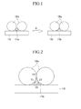
- FIGS. 1 and 2 An exemplary embodiment of a solar cell will be described with reference to FIGS. 1 and 2 .
- FIGS. 1 and 2 are schematic views of exemplary embodiments showing the conductive paste applied on the semiconductor substrate in one exemplary embodiment of a solar cell according to the present invention.
- the present invention is not limited to using the conductive paste within a solar cell and may be applied to other applications such as a PDP electrode or an OLED grid electrode.
- a conductive powder 120a and a metallic glass 115a included in the conductive paste may be present as particles, respectively.
- a glass transition temperature Tg of the metallic glass 115a is lower than an eutectic temperature of a semiconductor material, such as silicon, and the conductive powder 120a, when the conductive paste is applied on the semiconductor substrate 110 and heat-treated ( ⁇ ) at greater than a glass transition temperature Tg of the metallic glass 115a, the metallic glass 115a may be softened to fill the gap between a plurality of conductive powder 120a particles and the semiconductor substrate 110, to form a softened metallic glass 115b, as shown in FIG 1 .
- the softened metallic glass 115b may provide contact portions C1 and C2 with the conductive powder 120a, a contact portion C3 with a semiconductor substrate 110, and a contact portion C4 between neighboring particles of the conductive powder 120a to increase close contacting properties therebetween.
- the softened metallic glass closely contacts the conductive powder 120a and the semiconductor substrate 110, and thereby may provide a path for transferring electric charges generated by the semiconductor substrate 110 to the conductive powder 120a. That is, the distance between the conductive powders 120a particles or between the conductive powder 120a particles and the semiconductor substrate 110 is minimal.
- the softened metallic glass 115b may be formed as a buffer layer on the semiconductor substrate 110.
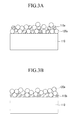
- FIGS. 3A to 3E are schematic views showing processes of providing a buffer layer on a semiconductor substrate applied with a conductive paste while increasing the temperature thereof.
- a conductive paste including the conductive powder 120a and the metallic glass 115a (here, the illustration of the organic vehicle is omitted) is applied on a semiconductor substrate 110.
- the temperature is increased to a temperature higher than the glass transition temperature Tg of the metallic glass 115a.
- the glass transition temperature Tg may range from about 450° C to about 500° C.
- the metallic glass 115b that is softened at a higher temperature than the glass transition temperature Tg may have wettability to contact the semiconductor substrate 110, and therefore closely contacts the semiconductor substrate 110.
- the softened metallic glass 115b has low viscosity, it may have high wettability, and therefore may increase the close contacting property thereof.
- the temperature is increased to a temperature higher than a sintering temperature Ts of the conductive powder 120a.
- the sintering temperature Ts may range from about 580° C to about 700° C.
- the adjacent conductive powder 120a may provide a firmly fastened and sintered conductive powder 120b at a temperature higher than the sintering temperature Ts.
- the metallic glass may exist as a solid, a supercooled liquid, or a liquid at the sintering temperature of the conductive powder 120a.
- temperature is increased to be greater than the eutectic temperature T1 of a sintered conductive powder 120b and the softened metallic glass 115b.
- the eutectic temperature may be about 780° C.
- the conductive powder 120b and the metallic glass 115b may be an eutectic mixture having an increased close contacting property, and the first eutectic layer 117 may be disposed between them.
- FIG. 3F is an enlarged view of Section 'A' (as indicated by dashed lines) shown in FIG. 3E .
- the temperature is increased to higher than the eutectic temperature T2 of the softened metallic glass 115b and the semiconductor substrate 110.
- the eutectic temperature may be about 802° C.
- the metallic glass 115b and the semiconductor substrate 110 may be an eutectic mixture having an increased close contacting property, and the second eutectic layer 118 may be disposed between them.
- the softened metallic glass 115b may provide a buffer layer 115 by being crystallized at a certain temperature, and the buffer layer 115 may prevent the conductive powder 120b from diffusing into the semiconductor substrate 110.
- a semiconductor substrate and an electrode are electrically connected to each other using a conductive metallic glass.
- loss of electric charges is decreased by enlarging the path for transferring the electric charges to the electrode from the semiconductor substrate, and a buffer layer including the metallic glass may prevent a conductive material of the electrode from deleteriously diffusing into the semiconductor substrate.
- exemplary embodiments of the conductive paste may further include glass frit.
- the glass frit may show a similar behavior as a metallic glass to form a part of a buffer layer and an eutectic layer.
- FIG. 4 another exemplary embodiment of a solar cell according to the present invention is described in detail.
- FIG. 4 is a cross-sectional view of an exemplary embodiment of a solar cell according to the present invention.
- a solar energy incident side of a semiconductor substrate 110 is called a front side, and the opposite side is called a rear side; although alternative configurations are possible.
- the exemplary embodiment of a solar cell according to the present invention may include a semiconductor substrate 110 including a lower semiconductor layer 110a and an upper semiconductor layer 110b.
- Exemplary embodiments of the semiconductor substrate 110 may be formed of a crystalline silicon or a compound semiconductor. Exemplary embodiments of the crystalline silicon may be, for example, a silicon wafer.
- One of the lower semiconductor layer 110a and the upper semiconductor layer 110b may be a semiconductor layer doped with a p-type impurity, and the other may be a semiconductor layer doped with an n-type impurity.
- the lower semiconductor layer 110a may be a semiconductor layer doped with a p-type impurity
- the upper semiconductor layer 110b may be a semiconductor layer doped with an n-type impurity.
- the p-type impurity may be a Group III element such as boron (B)
- the n-type impurity may be a Group V element such as phosphorus (P).
- the surface of the upper semiconductor layer 110b may be subjected to surface texturing.
- the surface-textured upper semiconductor layer 110b may have protrusions and depressions such as in a pyramid shape, or a porous structure such as a honeycomb or various other similar shapes.
- the surface-textured upper semiconductor layer 110b may have an enlarged surface area to enhance the light-absorption rate and decrease reflectivity, resultantly improving efficiency of a solar cell.
- a plurality of front electrodes 120 are disposed on the semiconductor layer 110b.
- the front electrodes 120 are arranged substantially in parallel to the plane of the substrate, and may be designed in a grid pattern with respect to shadowing loss and sheet resistance of the resulting solar cell.
- the front electrode 120 may be formed of a conductive material, for example a low resistance conductive material such as silver (Ag).
- the front electrode 120 may be disposed by a screen printing process using the conductive paste as described above.
- the conductive paste includes a conductive powder, a metallic glass, and an organic vehicle.
- a buffer layer 115 is disposed between the upper semiconductor layer 110b and the front electrode 120.
- the buffer layer 115 is a layer formed by softening the metallic glass in the conductive paste at a temperature greater than a glass transition temperature Tg of the metallic glass. Since the buffer layer 115 has conductivity due to the metallic glass and has parts that contact the electrode 120 and the upper semiconductor layer 110b, it may decrease loss of electric charges by enlarging the path for transferring electric charges between the upper semiconductor layer 110b and the front electrode 120. In addition, the buffer layer 115 may prevent a material of the front electrode 120 from deleteriously diffusing into the semiconductor substrate 110.
- a first eutectic layer 117 is disposed between the front electrode 120 and the buffer layer 115, and a second eutectic layer 118 is disposed between the buffer layer 115 and the upper semiconductor layer 110b.
- the first eutectic layer 117 includes an eutectic mixture of the conductive material included in the front electrode 120 and the metallic glass included in the buffer layer 115
- the second eutectic layer 118 includes an eutectic mixture of the metallic glass included in the buffer layer 115 and the semiconductor material included in the upper semiconductor layer 110b.
- a bus bar electrode (not shown) may be disposed on the front electrode 120.
- the bus bar electrode connects adjacent solar cells during assembly of a plurality of solar cells.
- a dielectric layer 130 is disposed under the semiconductor substrate 110.
- the dielectric layer 130 may increase efficiency of a solar cell by preventing recombination of electric charges and leaking of a current.
- the dielectric layer 130 may include a plurality of penetration parts 135, and the semiconductor substrate 110 and a rear electrode 140 that will be described in more detail below may contact one another through the penetration parts 135.
- the dielectric layer 130 may be formed with silicon oxide (SiO 2 ), silicon nitride (SiN x ), aluminum oxide (Al 2 O 3 ), a combination thereof or other materials with similar characteristics, and may have a thickness of about 100 ⁇ to about 2000 ⁇ .
- a rear electrode 140 is disposed under the dielectric layer 130.
- the rear electrode 140 may be formed of a conductive material, and in one exemplary embodiment it may be an opaque metal such as aluminum (Al).
- the rear electrode 140 may be disposed by a screen printing process using the above-mentioned conductive paste in the same manner as the front electrode 120.
- a buffer layer (not shown) is disposed between the rear electrode 140 and the lower semiconductor layer 110a in the same manner as the front electrode 120. Further, a first eutectic layer (not shown) is disposed between the rear electrode 140 and the buffer layer, and a second eutectic layer (not shown) is disposed between the lower semiconductor layer 110b and the buffer layer in the same manner as the front electrode 120.
- a semiconductor substrate 110 such as a silicon wafer is prepared.
- the semiconductor substrate 110 may be doped with a p-type impurity.
- the semiconductor substrate 110 is subjected to a surface texturing treatment.
- a surface texturing treatment may be performed by a wet method using a strong acid such as nitric acid and hydrofluoric acid or a strong base such as sodium hydroxide, or by a dry method using plasma.
- the semiconductor substrate 110 may be doped with an n-type impurity.
- the n-type impurity may be doped by diffusing POCl 3 or H 3 PO 4 or the like into the semiconductor substrate 110 at a high temperature.
- the semiconductor substrate 110 includes a lower semiconductor layer 110a and an upper semiconductor layer 110b doped with different impurities from each other.
- the conductive paste for a front electrode may be provided by a screen printing method.
- the screen printing method includes applying a front electrode conductive paste including a conductive powder such as silver (Ag), a metallic glass, and an organic vehicle on the position where a front electrode is positioned, and drying the same.
- a conductive paste may include a metallic glass, and the metallic glass may be prepared using any kind of method such as melt spinning, infiltration casting, gas atomization, ion irradiation, mechanical alloying or other similar methods.
- a dielectric layer 130 may be provided by stacking aluminum oxide (Al 2 O 3 ) or silicon oxide (SiO 2 ) on the rear side of the semiconductor substrate 110, as an example, by a plasma enhanced chemical vapor deposition (“PECVD”) method or other similar methods.
- PECVD plasma enhanced chemical vapor deposition
- a plurality of penetration parts 135 may be provided on one part of the dielectric layer 130 using a laser.
- the conductive paste for forming a rear electrode is subsequently applied on one side of the dielectric layer 130, e.g., by a screen printing.
- the conductive paste for forming a rear electrode is then dried.
- the conductive paste for forming a front electrode and the conductive paste for forming a rear electrode are co-fired.
- alternative exemplary embodiments include configurations wherein the conductive paste for a front electrode and the conductive paste for a rear electrode may be respectively fired.
- the firing may be performed at a higher temperature than the melting temperature of the conductive metal in a furnace, for example at a temperature ranging from about 400° C to about 1000° C.
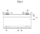
- FIG. 5 Another exemplary embodiment of a solar cell according to the present invention is described referring to FIG. 5 .
- FIG. 5 is a cross-sectional view showing another exemplary embodiment of a solar cell according to the present invention.
- an exemplary embodiment of a solar cell includes, as described with respect to the above-mentioned embodiment, a semiconductor substrate 110 including lower semiconductor layer 110a and upper semiconductor layer 110b; a plurality of front electrodes 120; a buffer layer 115 positioned between an upper semiconductor layer 110b and the front electrodes 120; a first eutectic layer 117 positioned between the front electrode 120 and the buffer layer 115; a second eutectic layer 118 positioned between the upper semiconductor layer 110b and the buffer layer 115; a dielectric layer 130 positioned under the semiconductor substrate 110; and a rear electrode 140 positioned under the dielectric layer 130.
- the solar cell according to the present embodiment unlike the above-mentioned embodiment, includes an insulating layer 112 covering the entire surface of the semiconductor substrate 110 except the regions corresponding to the buffer layer 115 as described in more detail below.
- Exemplary embodiments of the insulating layer 112 may be made of insulating material that absorbs relatively little light, for example, silicon nitride (SiN x ), silicon oxide (SiO 2 ), titanium oxide (TiO 2 ), aluminum oxide (Al 2 O 3 ), magnesium oxide (MgO), cerium oxide (CeO 2 ), a combination thereof, or other materials with similar characteristics.
- Exemplary embodiments of the insulating layer 112 include a single layer configuration and a multiple layer configuration.
- the insulating layer 112 may have a thickness ranging from about 200 ⁇ to about 1500 ⁇ .
- the insulating layer 112 may decrease the reflection rate of light and increase selectivity of a particular wavelength or a particular range of wavelengths on the front side of the solar cell to serve as an anti-reflective coating ("ARC").
- the insulating layer 112 may be manufactured from a material that is effective to improve its contact properties with the silicon in the surface of the semiconductor substrate 110, thereby increasing the efficiency of the solar cell.
- the front electrodes 120 may penetrate the insulating layer 112 to contact the upper semiconductor layer 110b.
- the contacting part of the front electrode 120 and the upper semiconductor layer 110b may be removed by etching, and the etching may be carried out by using the conductive paste further including glass frit with the conductive powder, the metallic glass and the organic vehicle.
- the glass frit may have an etching property with respect to the insulating layer 112.
- the glass frit may act as the metallic glass, and by further including the glass frit with metallic glass, it may improve adhesion to a lower layer.
- FIG. 6 Another exemplary embodiment of a solar cell according to the present invention is described referring to FIG. 6 .
- FIG. 6 is a cross-sectional view showing another exemplary embodiment of a solar cell according to the present invention.
- the present exemplary embodiment of a solar cell may include a semiconductor substrate 110 doped with a p-type or an n-type impurity.
- the semiconductor substrate 110 may include a plurality of first doping regions 111a and second doping regions 111b that are provided on the rear side and are doped with different impurities from each other.
- the first doping regions 111a may be doped with an n-type impurity
- the second doping regions 111b may be doped with a p-type impurity.
- the first doping regions 111a and the second doping regions 111b may be alternately disposed in the rear side of the semiconductor substrate 110.
- the front side of the semiconductor substrate 110 may be surface-textured, and therefore may enhance the light-absorption rate and decrease the reflectivity thereof, resultantly improving efficiency of a resulting solar cell.
- an insulation layer 112 is provided on the semiconductor substrate 110.
- a dielectric layer 150 including a plurality of penetration parts may be disposed on the rear side of the semiconductor substrate 110.
- the first electrode 121 connected with the first doping region 111a and the second electrode 141 connected with the second doping region 111b are disposed on the rear side of the semiconductor substrate 110, respectively.
- the first electrode 121 and the first doping region 111a may be contacted with one another through a penetration part
- the second electrode 141 and the second doping region 111b may be contacted with one another through a penetration part.
- the first electrode 121 and the second electrode 141 may be alternately disposed with one another.
- the first electrode 121 and the second electrode 141 may be disposed on the semiconductor 110 using a conductive paste including a conductive powder, a metallic glass, an organic vehicle, and optionally glass frit, which is substantially the same as described above.
- a buffer layer 115 is disposed between the first doping region 111a and the first electrode 121, and/or between the second doping region 111b and the second electrode 141.
- the buffer layer 115 may have conductivity due to a metallic glass used in the formation thereof. Since the buffer layer 115 includes parts contacting the first electrode 121 and/or the second electrode 141 and parts contacting the first doping region 111a and/or the second doping region 111b, loss of electric charges may decrease by enlarging the path for charge transfer between the first doping region 111a and the first electrode 121, and/or between the second doping region 111b and the second electrode 141. In addition, the buffer layer 115 may prevent a material of the first electrode 121 or the second electrode 141 from deleteriously diffusing into the first or second doping region 111a or 111b.
- An exemplary embodiment of a solar cell including both of the first electrode 121 and the second electrode 141 on the rear surface of the solar cell may decrease an area where a metal is positioned on the front, i.e., light incident, surface of the solar cell. This may decrease shadowing loss and increase solar cell efficiency.
- a semiconductor substrate 110 doped with, for example, an n-type impurity is prepared. Then, the semiconductor substrate 110 is surface-textured, and insulation layer 112 and dielectric layer 150 are disposed on front side and rear side of the semiconductor substrate 110, respectively.
- the insulation layer 112 and the dielectric layer 150 may be provided by chemical vapor deposition ("CVD").
- a part of the dielectric layer 150 is removed by, for example, using a laser to form a plurality of openings.
- the first doping region 111a and the second doping region 111b may be disposed by sequentially doping a p-type impurity and an n-type impurity at a high concentration in the openings at rear side of the semiconductor substrate 110.
- a conductive paste for forming a first electrode 121 is applied on one side of the dielectric layer 150 corresponding to the first doping region 111a, and a conductive paste for forming a second electrode is applied on the other side corresponding to the second doping region 111b.
- the conductive paste for forming a first electrode and the conductive paste for forming a second electrode are provided by a screen printing process, and the conductive paste including a conductive powder, a metallic glass, an organic vehicle, and optionally glass frit may be respectively used.
- the conductive paste for forming a front electrode and the conductive paste for forming a rear electrode may be fired together or respectively.
- the firing may be performed at a higher temperature than the melting temperature of a conductive metal in a furnace.
Landscapes
- Chemical & Material Sciences (AREA)
- Dispersion Chemistry (AREA)
- Inorganic Chemistry (AREA)
- Physics & Mathematics (AREA)
- Spectroscopy & Molecular Physics (AREA)
- Photovoltaic Devices (AREA)
- Conductive Materials (AREA)
- Life Sciences & Earth Sciences (AREA)
- Engineering & Computer Science (AREA)
- Sustainable Development (AREA)
- Sustainable Energy (AREA)
Abstract
Description
- This disclosure relates to a conductive paste and a solar cell utilizing the same.
- A solar cell is a photoelectric conversion device that transforms photonic energy, e.g., solar energy, into electrical energy, and it has attracted much attention as a renewable and pollution-free next generation energy source.
- A solar cell typically includes p-type and n-type semiconductors and produces electrical energy by transferring electrons and holes to the n-type and p-type semiconductors, respectively, and then collecting the electrons and holes in each of a pair of oppositely disposed electrodes, when an electron-hole pair ("EHP") including electron and hole charge carries is produced by the absorption of solar light energy in a photoactive layer inside the semiconductors.
- Furthermore, it is typically beneficial for a solar cell to be as efficient as possible for producing electrical energy from solar energy. In order to improve solar energy conversion efficiency, the solar cell may be able to effectively absorb light with little loss so that it may produce as many electron-hole pairs as possible, and then collect the produced charges without losses of the electrons or holes.
- Furthermore, an electrode of a solar cell may be fabricated by screen printing using a conductive paste.
- One aspect of the present invention provides a conductive paste that may reduce loss of electrical charges and improve efficiency of a solar cell.
- Another aspect of the present invention provides a solar cell using the conductive paste.
- According to one aspect, a conductive paste including; a conductive powder including a plurality of conductive particles, a metallic glass disposed between adjacent conductive particles of the conductive powder, and an organic vehicle in which the conductive powder and metallic glass are disposed is provided.
- In one exemplary embodiment, the metallic glass may include at least one of copper (Cu), titanium (Ti), nickel (Ni), zirconium (Zr), iron (Fe), magnesium (Mg), calcium (Ca), cobalt (Co), palladium (Pd), platinum (Pt), gold (Au), cerium (Ce), lanthanum (La), yttrium (Y), gadolinium (Gd), beryllium (Be), tantalum (Ta), gallium (Ga), aluminum (Al), hafnium (Hf), niobium (Nb), lead (Pb), silver (Ag), phosphorus (P), boron (B), silicon (Si), carbon (C), tin (Sn), zinc (Zn), molybdenum (Mo), tungsten (W), manganese (Mn), erbium (Er), chromium (Cr), praseodymium (Pr), thulium (Tm), or a combination thereof.
- In one exemplary embodiment, the metallic glass may include an alloy of copper (Cu), zirconium (Zr), nickel (Ni), iron (Fe), titanium (Ti), magnesium (Mg), or a combination thereof.
- In one exemplary embodiment, a glass transition temperature (Tg) of the metallic glass may be lower than an eutectic temperature of silicon and the conductive powder.
- In one exemplary embodiment, an eutectic temperature of the conductive powder and the metallic glass may be lower than that of the silicon and the conductive powder.
- In one exemplary embodiment, an eutectic temperature of the silicon and the metallic glass may be lower than that of the silicon and the conductive powder.
- In one exemplary embodiment, the metallic glass may exist as one of a solid, a supercooled liquid, and a liquid at a sintering temperature of the conductive powder.
- In one exemplary embodiment, the conductive powder may include at least one of silver (Ag), aluminum (Al), copper (Cu), nickel (Ni), and a combination thereof.
- In one exemplary embodiment, the conductive paste may include about 50 wt% to about 90 wt% of the conductive powder, about 1 wt% to about 20 wt% of the metallic glass, and a remaining amount of the organic vehicle based on a total amount of the conductive paste.
- In one exemplary embodiment, the conductive paste may further include glass frit.
- In one exemplary embodiment, the conductive paste may include about 50 wt% to about 90 wt% of the conductive powder, about 1 wt% to about 20 wt% of the metallic glass, about 1 wt% to 10 wt% of the glass frit, and a remaining amount of the organic vehicle based on a total amount of the conductive paste.
- According to another exemplary embodiment, the solar cell may include a semiconductor layer including a semiconductor material, an electrode including a conductive material electrically connected to the semiconductor layer, and a buffer layer including a metallic glass contacted with the semiconductor layer and the electrode.
- In one exemplary embodiment, the buffer layer may be disposed between the semiconductor layer and the electrode.
- In one exemplary embodiment, a glass transition temperature of the metallic glass may be lower than the eutectic temperature of the semiconductor material and the conductive material.
- In one exemplary embodiment, an eutectic temperature of the conductive material and the metallic glass may be lower than the eutectic temperature of the semiconductor material and the conductive material.
- In one exemplary embodiment, an eutectic temperature of the semiconductor material and the metallic glass may be lower than an eutectic temperature of the semiconductor material and the conductive material.
- In one exemplary embodiment, the buffer layer may further include glass frit.
- In one exemplary embodiment, the semiconductor material may include silicon.
- In one exemplary embodiment, the solar cell may further include a first eutectic layer where the conductive material and the metallic glass are subjected to eutectic melting.
- In one exemplary embodiment, the solar cell may further include a second eutectic layer that is disposed between the semiconductor layer and the buffer layer and where the semiconductor material and the metallic glass are subjected to eutectic melting.
- In one exemplary embodiment, the second eutectic layer may be where the semiconductor material, the metallic glass, and glass frit are subjected to eutectic melting.
- In one exemplary embodiment, the metallic glass may be an alloy including at least one of copper (Cu), titanium (Ti), nickel (Ni), zirconium (Zr), iron (Fe), magnesium (Mg), calcium (Ca), cobalt (Co), palladium (Pd), platinum (Pt), gold (Au), cerium (Ce), lanthanum (La), yttrium (Y), gadolinium (Gd), beryllium (Be), tantalum (Ta), gallium (Ga), aluminum (Al), hafnium (Hf), niobium (Nb), lead (Pb), silver (Ag), phosphorus (P), boron (B), silicon (Si), carbon (C), tin (Sn), zinc (Zn), molybdenum (Mo), tungsten (W), manganese (Mn), erbium (Er), chromium (Cr), praseodymium (Pr), thulium (Tm), or a combination thereof.
- In one exemplary embodiment, the conductive material may include silver (Ag), aluminum (Al), copper (Cu), nickel (Ni), or a combination thereof.
- In one exemplary embodiment, the semiconductor layer may include a p-type layer doped with a p-type impurity and an n-type layer doped with an n-type impurity, the electrode may include a first electrode electrically connected with the p-type layer and a second electrode electrically connected with the n-type layer, and the buffer layer may be disposed at at least one of between the p-type layer and the first electrode and the n-type layer and the second electrode.
- The above and other aspects, advantages and features of this disclosure will become more apparent by describing in further detail exemplary embodiments thereof with reference to the accompanying drawings, in which:
-
FIGS. 1 and 2 are schematic views of exemplary embodiments showing a conductive powder applied on a semiconductor substrate in an exemplary embodiment of a solar cell according to the present invention; -
FIGS. 3A to 3F are schematic views showing exemplary embodiments of processes of providing a buffer layer on a semiconductor substrate applied with a conductive paste while increasing the temperature thereof; -
FIG. 4 is a cross-sectional view of an exemplary embodiment of a solar cell according to the present invention; -
FIG. 5 is a cross-sectional view of another exemplary embodiment of a solar cell according to the present invention; and -
FIG. 6 is a cross-sectional view of another exemplary embodiment of a solar cell according to the present invention. - The invention now will be described more fully hereinafter with reference to the accompanying drawings, in which embodiments of the invention are shown. This invention may, however, be embodied in many different forms and should not be construed as limited to the embodiments set forth herein. Rather, these embodiments are provided so that this disclosure will be thorough and complete, and will fully convey the scope of the invention to those skilled in the art. Like reference numerals refer to like elements throughout.
- It will be understood that when an element is referred to as being "on" another element, it can be directly on the other element or intervening elements may be present therebetween. In contrast, when an element is referred to as being "directly on" another element, there are no intervening elements present. As used herein, the term "and/or" includes any and all combinations of one or more of the associated listed items.
- It will be understood that, although the terms first, second, third etc. may be used herein to describe various elements, components, regions, layers and/or sections, these elements, components, regions, layers and/or sections should not be limited by these terms. These terms are only used to distinguish one element, component, region, layer or section from another element, component, region, layer or section. Thus, a first element, component, region, layer or section discussed below could be termed a second element, component, region, layer or section without departing from the teachings of the present invention.
- The terminology used herein is for the purpose of describing particular embodiments only and is not intended to be limiting of the invention. As used herein, the singular forms "a", "an" and "the" are intended to include the plural forms as well, unless the context clearly indicates otherwise. It will be further understood that the terms "comprises" and/or "comprising," or "includes" and/or "including" when used in this specification, specify the presence of stated features, regions, integers, steps, operations, elements, and/or components, but do not preclude the presence or addition of one or more other features, regions, integers, steps, operations, elements, components, and/or groups thereof.
- Furthermore, relative terms, such as "lower" or "bottom" and "upper" or "top," may be used herein to describe one element's relationship to another elements as illustrated in the Figures. It will be understood that relative terms are intended to encompass different orientations of the device in addition to the orientation depicted in the Figures. For example, if the device in one of the figures is turned over, elements described as being on the "lower" side of other elements would then be oriented on "upper" sides of the other elements. The exemplary term "lower", can therefore, encompasses both an orientation of "lower" and "upper," depending on the particular orientation of the figure. Similarly, if the device in one of the figures is turned over, elements described as "below" or "beneath" other elements would then be oriented "above" the other elements. The exemplary terms "below" or "beneath" can, therefore, encompass both an orientation of above and below.
- Unless otherwise defined, all terms (including technical and scientific terms) used herein have the same meaning as commonly understood by one of ordinary skill in the art to which this invention belongs. It will be further understood that terms, such as those defined in commonly used dictionaries, should be interpreted as having a meaning that is consistent with their meaning in the context of the relevant art and the present disclosure, and will not be interpreted in an idealized or overly formal sense unless expressly so defined herein.
- Exemplary embodiments of the present invention are described herein with reference to cross section illustrations that are schematic illustrations of idealized embodiments of the present invention. As such, variations from the shapes of the illustrations as a result, for example, of manufacturing techniques and/or tolerances, are to be expected. Thus, embodiments of the present invention should not be construed as limited to the particular shapes of regions illustrated herein but are to include deviations in shapes that result, for example, from manufacturing. For example, a region illustrated or described as flat may, typically, have rough and/or nonlinear features. Moreover, sharp angles that are illustrated may be rounded. Thus, the regions illustrated in the figures are schematic in nature and their shapes are not intended to illustrate the precise shape of a region and are not intended to limit the scope of the present invention.
- All methods described herein can be performed in a suitable order unless otherwise indicated herein or otherwise clearly contradicted by context. The use of any and all examples, or exemplary language (e.g., "such as"), is intended merely to better illustrate the invention and does not pose a limitation on the scope of the invention unless otherwise claimed. No language in the specification should be construed as indicating any non-claimed element as essential to the practice of the invention as used herein.
- Hereinafter, the present invention will be described in detail with reference to the accompanying drawings.
- First, an exemplary embodiment of a conductive paste according to the present invention will be explained in detail.
- According to the present exemplary embodiment, the conductive paste includes a conductive powder, a metallic glass, and an organic vehicle.
- The conductive powder includes aluminum (Al), or an aluminum (Al)-containing metal such as an aluminum alloy, silver (Ag), or a silver (Ag)-containing metal such as a silver alloy, copper (Cu), or a copper (Cu)-containing metal such as a copper alloy, nickel (Ni), or a nickel (Ni)-containing metal such as a nickel alloy, a combination thereof or other materials with similar characteristics. Exemplary embodiments include configurations wherein the conductive powder may include other metals, and may include different additives besides the above mentioned metals. In one exemplary embodiment, the conductive powder may have a size of about 0.1 µm to about 50 µm.
- The metallic glass includes an alloy having a disordered atomic structure including two or more metals, and is also referred to as an amorphous metal. Since the metallic glass has low resistance that is different from a regular glass such as a silicate, it may be considered an electrical conductor at voltages and currents typically applied to a solar cell.
- The metallic glass may be an alloy of transition elements, a noble metal, a rare earth element metal, an alkaline-earth metal, a semimetal, and a combination thereof, and the alloy may include at least one of copper (Cu), titanium (Ti), nickel (Ni), zirconium (Zr), iron (Fe), magnesium (Mg), calcium (Ca), cobalt (Co), palladium (Pd), platinum (Pt), gold (Au), cerium (Ce), lanthanum (La), yttrium (Y), gadolinium (Gd), beryllium (Be), tantalum (Ta), gallium (Ga), aluminum (Al), hafnium (Hf), niobium (Nb), lead (Pb), silver (Ag), phosphorus (P), boron (B), silicon (Si), carbon (C), tin (Sn), zinc (Zn), molybdenum (Mo), tungsten (W), manganese (Mn), erbium (Er), chromium (Cr), praseodymium (Pr), thulium (Tm), a combination thereof or other materials with similar characteristics.
- In one exemplary embodiment, the metallic glass may include at least one selected from copper (Cu), zirconium (Zr), nickel (Ni), iron (Fe), titanium (Ti), magnesium (Mg), and a combination thereof.
- Exemplary embodiments of the metallic glass may include Cu50Zr50, Cu30Ag30Zr30Ti10, CU43Zr43Al7Ag7, Cu46Zr46Al8, CU58.1Zr35.9Al6, Ti50Ni15Cu32Sn3, Ti45Ni15CU25Sn3Be7Zr5, Ni60Nb30Ta10, Ni61Zr20Nb7Al4Ta8, Ni57.5Zr35Al7.5, Zr41.2Ti13.8Ni10CU12.5Be22.5, Mg65Y10CU15Ag5Pd5, Mn55Al25Ni20, La55Al25Ni10Cu10, Mg65Cu75Ni75Ag5Zn5Gd10, Mg65CU15Ag10Y6Gd4, Fe77Nb6B17, Fe67Mo13B17Y3, Ca65Mg15Zn20, Ca66.4Al33.6, a combination thereof or other materials with similar characteristics, but is not limited thereto.
- The metallic glass may be softened once heated to a glass transition temperature (Tg) or greater, similar to a regular, e.g., non-metallic, glass.
- Herein, the glass transition temperature Tg of the metallic glass may be lower than the eutectic temperature of a semiconductor material such as silicon and the conductive powder. Accordingly, the metallic glass may be softened at a temperature lower than the eutectic melting of the semiconductor material and the conductive powder, and therefore the softening may occur prior to eutectic melting of the semiconductor material and the conductive powder during a heating process.
- The eutectic temperature of the conductive powder and the metallic glass may be lower than the eutectic temperature of the semiconductor material and the conductive powder. Accordingly, the conductive powder and the metallic glass may be eutectically melted before the eutectic melting of the semiconductor material and the conductive powder during a heating process as described above.
- Also, the eutectic temperature of the semiconductor material and the metallic glass may be lower than the eutectic temperature of the semiconductor material and the conductive powder. Accordingly, the semiconductor material and the metallic glass may be eutectically melted before the eutectic melting of the conductive powder and the semiconductor material.
- The metallic glass may exist as a solid, a supercooled liquid, or a liquid when heated to a sintering temperature of the conductive powder.
- In short, when the conductive paste is applied on the semiconductor layer made of semiconductor material and the temperature is increased, e.g., from a room temperature, the metallic glass is first softened and the softened metallic glass widens an electric charge transfer passage between a semiconductor material and a conductive material by extending a contact area between the semiconductor substrate and a conductive powder. Afterward, the eutectic melting of the metallic glass and the conductive powder, the eutectic melting of the metallic glass and the semiconductor material, and the eutectic melting of the semiconductor material and the conductive powder may be carried out.
- The organic vehicle may include an organic compound mixed with a conductive powder and a metallic glass that imparts viscosity to the organic vehicle, and a solvent dissolving the above components.
- Exemplary embodiments of the organic compound may include at least one of a (meth)acrylate resin; a cellulose resin such as ethyl cellulose; a phenol resin; an alcohol resin; tetrafluoroethylene (TEFLON); and a combination thereof, and furthermore, it may include an additive such as a surfactant, a thickening agent, a stabilizer and other similar elements.
- The solvent may include any kind of solvent as long as it may be soluble with the components.
- In one exemplary embodiment, the conductive paste may include about 50 wt% to about 90 wt% of the conductive powder, about 1 wt% to about 20 wt% of the metallic glass, and the balance amount of the conductive paste may be the organic vehicle based on the total amount of the conductive paste.
- In one exemplary embodiment, the conductive paste may further include glass frit.
- In the embodiment where it is included, the glass frit has an etching property that etches an insulating layer such as anti-reflective layer in a solar cell to penetrate the insulating layer. Accordingly, the conductive paste including the glass frit may be used in a solar cell provided with an anti-reflective layer.
- Also, the glass frit may have an excellent adhesion with a lower layer to improve an adhesion between an electrode made of the conductive paste and a lower layer.
- Exemplary embodiments of the glass frit may include PbO-SiO2, PbO-SiO2-B2O3, PbO-SiO2-B2O3-ZnO, PbO-SiO2-B2O3-BaO, PbO-SiO2-ZnO-BaO, ZnO-SiO2, ZnO-B2O3-SiO2, ZnO-K2O-B2O3-SiO2-BaO, Bi2O3-SiO2, Bi2O3-B2O3-SiO2, Bi2O3-B2O3-SiO2-BaO, ZnO-BaO-B2O3-B2O5-Na2O, Bi2O3-B2O3-SiO2-BaO-ZnO, a combination thereof or other materials with similar characteristics.
- In an exemplary embodiment wherein the glass frit is included, the conductive paste may include about 50 wt% to about 90 wt% of the conductive powder, about 1 wt% to about 20 wt% of the metallic glass, about 1 wt% to about 10 wt% of the glass frit, and the balance amount of the conductive paste may be the organic vehicle based on the total amount of the conductive paste.
- Exemplary embodiments include configurations wherein the conductive paste including the conductive powder, the metallic glass and the organic vehicle may be applied by, for example, screen-printing, when an electrode is formed in various electronic devices. The electronic devices may include a solar cell.
- When the electrode is formed in a solar cell, above-mentioned conductive paste may be applied on a semiconductor substrate such as silicon wafer and fired, e.g., heated and dried, to form an electrode.
- Hereinafter, an exemplary embodiment of a solar cell will be described with reference to
FIGS. 1 and 2 . -
FIGS. 1 and 2 are schematic views of exemplary embodiments showing the conductive paste applied on the semiconductor substrate in one exemplary embodiment of a solar cell according to the present invention. The present invention is not limited to using the conductive paste within a solar cell and may be applied to other applications such as a PDP electrode or an OLED grid electrode. - Referring to
FIG. 1 , when an exemplary embodiment of a conductive paste according to the present invention is applied on thesemiconductor substrate 110, aconductive powder 120a and ametallic glass 115a included in the conductive paste may be present as particles, respectively. - As mentioned above, since a glass transition temperature Tg of the
metallic glass 115a is lower than an eutectic temperature of a semiconductor material, such as silicon, and theconductive powder 120a, when the conductive paste is applied on thesemiconductor substrate 110 and heat-treated (Δ) at greater than a glass transition temperature Tg of themetallic glass 115a, themetallic glass 115a may be softened to fill the gap between a plurality ofconductive powder 120a particles and thesemiconductor substrate 110, to form a softenedmetallic glass 115b, as shown inFIG 1 . - Referring to
FIG. 2 , the softenedmetallic glass 115b may provide contact portions C1 and C2 with theconductive powder 120a, a contact portion C3 with asemiconductor substrate 110, and a contact portion C4 between neighboring particles of theconductive powder 120a to increase close contacting properties therebetween. The softened metallic glass closely contacts theconductive powder 120a and thesemiconductor substrate 110, and thereby may provide a path for transferring electric charges generated by thesemiconductor substrate 110 to theconductive powder 120a. That is, the distance between theconductive powders 120a particles or between theconductive powder 120a particles and thesemiconductor substrate 110 is minimal. - The softened
metallic glass 115b may be formed as a buffer layer on thesemiconductor substrate 110. - Hereinafter, the formation of the softened
metallic glass 115b as a buffer layer on thesemiconductor substrate 110 will be described in detail referring toFIGS. 3A to 3E . -
FIGS. 3A to 3E are schematic views showing processes of providing a buffer layer on a semiconductor substrate applied with a conductive paste while increasing the temperature thereof. - Referring to
FIG. 3A , a conductive paste including theconductive powder 120a and themetallic glass 115a (here, the illustration of the organic vehicle is omitted) is applied on asemiconductor substrate 110. - Referring to
FIG. 3B , the temperature is increased to a temperature higher than the glass transition temperature Tg of themetallic glass 115a. In the exemplary embodiment wherein themetallic glass 115a includes Cu50Zr40Al10, the glass transition temperature Tg may range from about 450° C to about 500° C. Themetallic glass 115b that is softened at a higher temperature than the glass transition temperature Tg may have wettability to contact thesemiconductor substrate 110, and therefore closely contacts thesemiconductor substrate 110. When the softenedmetallic glass 115b has low viscosity, it may have high wettability, and therefore may increase the close contacting property thereof. - Referring to
FIG. 3C , the temperature is increased to a temperature higher than a sintering temperature Ts of theconductive powder 120a. In the exemplary embodiment wherein theconductive powder 120a is silver (Ag), the sintering temperature Ts may range from about 580° C to about 700° C. The adjacentconductive powder 120a may provide a firmly fastened and sinteredconductive powder 120b at a temperature higher than the sintering temperature Ts. The metallic glass may exist as a solid, a supercooled liquid, or a liquid at the sintering temperature of theconductive powder 120a. - Referring to
FIG. 3D , temperature is increased to be greater than the eutectic temperature T1 of a sinteredconductive powder 120b and the softenedmetallic glass 115b. In the exemplary embodiment wherein theconductive powder 120b is silver (Ag) and themetallic glass 115b is Cu50Zr40Al10, the eutectic temperature may be about 780° C. Theconductive powder 120b and themetallic glass 115b may be an eutectic mixture having an increased close contacting property, and thefirst eutectic layer 117 may be disposed between them. - Referring to
FIGS. 3E and 3F , whereinFIG. 3F is an enlarged view of Section 'A' (as indicated by dashed lines) shown inFIG. 3E . the temperature is increased to higher than the eutectic temperature T2 of the softenedmetallic glass 115b and thesemiconductor substrate 110. In the exemplary embodiment wherein themetallic glass 115b includes Cu50Zr40Al10 and thesemiconductor substrate 110 includes silicon, the eutectic temperature may be about 802° C. Themetallic glass 115b and thesemiconductor substrate 110 may be an eutectic mixture having an increased close contacting property, and thesecond eutectic layer 118 may be disposed between them. - The softened
metallic glass 115b may provide abuffer layer 115 by being crystallized at a certain temperature, and thebuffer layer 115 may prevent theconductive powder 120b from diffusing into thesemiconductor substrate 110. - In the present exemplary embodiment, a semiconductor substrate and an electrode are electrically connected to each other using a conductive metallic glass. Thereby, loss of electric charges is decreased by enlarging the path for transferring the electric charges to the electrode from the semiconductor substrate, and a buffer layer including the metallic glass may prevent a conductive material of the electrode from deleteriously diffusing into the semiconductor substrate.
- Meanwhile, as mentioned above, exemplary embodiments of the conductive paste may further include glass frit. The glass frit may show a similar behavior as a metallic glass to form a part of a buffer layer and an eutectic layer.
- Referring to
FIG. 4 , another exemplary embodiment of a solar cell according to the present invention is described in detail. -
FIG. 4 is a cross-sectional view of an exemplary embodiment of a solar cell according to the present invention. - Hereinafter, positions of components will be described with respect to a vertical relation to a
semiconductor substrate 110 for better understanding and ease of description, but the present invention is not limited thereto. In addition, as used herein a solar energy incident side of asemiconductor substrate 110 is called a front side, and the opposite side is called a rear side; although alternative configurations are possible. - Referring to
FIG. 4 , the exemplary embodiment of a solar cell according to the present invention may include asemiconductor substrate 110 including alower semiconductor layer 110a and anupper semiconductor layer 110b. - Exemplary embodiments of the
semiconductor substrate 110 may be formed of a crystalline silicon or a compound semiconductor. Exemplary embodiments of the crystalline silicon may be, for example, a silicon wafer. One of thelower semiconductor layer 110a and theupper semiconductor layer 110b may be a semiconductor layer doped with a p-type impurity, and the other may be a semiconductor layer doped with an n-type impurity. For example, in one exemplary embodiment thelower semiconductor layer 110a may be a semiconductor layer doped with a p-type impurity, and theupper semiconductor layer 110b may be a semiconductor layer doped with an n-type impurity. Herein, in one exemplary embodiment the p-type impurity may be a Group III element such as boron (B), and the n-type impurity may be a Group V element such as phosphorus (P). - In one exemplary embodiment, the surface of the
upper semiconductor layer 110b may be subjected to surface texturing. The surface-texturedupper semiconductor layer 110b may have protrusions and depressions such as in a pyramid shape, or a porous structure such as a honeycomb or various other similar shapes. The surface-texturedupper semiconductor layer 110b may have an enlarged surface area to enhance the light-absorption rate and decrease reflectivity, resultantly improving efficiency of a solar cell. - A plurality of
front electrodes 120 are disposed on thesemiconductor layer 110b. Thefront electrodes 120 are arranged substantially in parallel to the plane of the substrate, and may be designed in a grid pattern with respect to shadowing loss and sheet resistance of the resulting solar cell. - In one exemplary embodiment, the
front electrode 120 may be formed of a conductive material, for example a low resistance conductive material such as silver (Ag). Thefront electrode 120 may be disposed by a screen printing process using the conductive paste as described above. As mentioned above, the conductive paste includes a conductive powder, a metallic glass, and an organic vehicle. - A
buffer layer 115 is disposed between theupper semiconductor layer 110b and thefront electrode 120. Thebuffer layer 115 is a layer formed by softening the metallic glass in the conductive paste at a temperature greater than a glass transition temperature Tg of the metallic glass. Since thebuffer layer 115 has conductivity due to the metallic glass and has parts that contact theelectrode 120 and theupper semiconductor layer 110b, it may decrease loss of electric charges by enlarging the path for transferring electric charges between theupper semiconductor layer 110b and thefront electrode 120. In addition, thebuffer layer 115 may prevent a material of thefront electrode 120 from deleteriously diffusing into thesemiconductor substrate 110. - A
first eutectic layer 117 is disposed between thefront electrode 120 and thebuffer layer 115, and asecond eutectic layer 118 is disposed between thebuffer layer 115 and theupper semiconductor layer 110b. Thefirst eutectic layer 117 includes an eutectic mixture of the conductive material included in thefront electrode 120 and the metallic glass included in thebuffer layer 115, and thesecond eutectic layer 118 includes an eutectic mixture of the metallic glass included in thebuffer layer 115 and the semiconductor material included in theupper semiconductor layer 110b. - In an exemplary embodiment wherein the solar cell is part of a larger solar array, a bus bar electrode (not shown) may be disposed on the
front electrode 120. The bus bar electrode connects adjacent solar cells during assembly of a plurality of solar cells. - A
dielectric layer 130 is disposed under thesemiconductor substrate 110. Thedielectric layer 130 may increase efficiency of a solar cell by preventing recombination of electric charges and leaking of a current. Thedielectric layer 130 may include a plurality ofpenetration parts 135, and thesemiconductor substrate 110 and arear electrode 140 that will be described in more detail below may contact one another through thepenetration parts 135. - In one exemplary embodiment, the
dielectric layer 130 may be formed with silicon oxide (SiO2), silicon nitride (SiNx), aluminum oxide (Al2O3), a combination thereof or other materials with similar characteristics, and may have a thickness of about 100 Å to about 2000 Å. - A
rear electrode 140 is disposed under thedielectric layer 130. Therear electrode 140 may be formed of a conductive material, and in one exemplary embodiment it may be an opaque metal such as aluminum (Al). Therear electrode 140 may be disposed by a screen printing process using the above-mentioned conductive paste in the same manner as thefront electrode 120. - In one exemplary embodiment, a buffer layer (not shown) is disposed between the
rear electrode 140 and thelower semiconductor layer 110a in the same manner as thefront electrode 120. Further, a first eutectic layer (not shown) is disposed between therear electrode 140 and the buffer layer, and a second eutectic layer (not shown) is disposed between thelower semiconductor layer 110b and the buffer layer in the same manner as thefront electrode 120. - Hereinafter, an exemplary embodiment of the conductive paste used for manufacturing the exemplary embodiment of a solar cell will be described in more detail.
- Hereinafter, an exemplary embodiment of a method of manufacturing an exemplary embodiment of a solar cell using the conductive paste will be described with reference to
FIG. 4 . - First, a
semiconductor substrate 110 such as a silicon wafer is prepared. In one exemplary embodiment, thesemiconductor substrate 110 may be doped with a p-type impurity. - Then the
semiconductor substrate 110 is subjected to a surface texturing treatment. Exemplary embodiments of the surface-texturing treatment may be performed by a wet method using a strong acid such as nitric acid and hydrofluoric acid or a strong base such as sodium hydroxide, or by a dry method using plasma. - Then, in one exemplary embodiment the
semiconductor substrate 110 may be doped with an n-type impurity. The n-type impurity may be doped by diffusing POCl3 or H3PO4 or the like into thesemiconductor substrate 110 at a high temperature. Thus, thesemiconductor substrate 110 includes alower semiconductor layer 110a and anupper semiconductor layer 110b doped with different impurities from each other. - Then a conductive paste for a front electrode is applied on the
upper semiconductor layer 110b. The conductive paste for a front electrode may be provided by a screen printing method. The screen printing method includes applying a front electrode conductive paste including a conductive powder such as silver (Ag), a metallic glass, and an organic vehicle on the position where a front electrode is positioned, and drying the same. - As described above, a conductive paste may include a metallic glass, and the metallic glass may be prepared using any kind of method such as melt spinning, infiltration casting, gas atomization, ion irradiation, mechanical alloying or other similar methods.
- Then the conductive paste for forming a front electrode is dried.
- A
dielectric layer 130 may be provided by stacking aluminum oxide (Al2O3) or silicon oxide (SiO2) on the rear side of thesemiconductor substrate 110, as an example, by a plasma enhanced chemical vapor deposition ("PECVD") method or other similar methods. - Then, in one exemplary embodiment, a plurality of
penetration parts 135 may be provided on one part of thedielectric layer 130 using a laser. - The conductive paste for forming a rear electrode is subsequently applied on one side of the
dielectric layer 130, e.g., by a screen printing. - The conductive paste for forming a rear electrode is then dried.
- Next, in the present exemplary embodiment the conductive paste for forming a front electrode and the conductive paste for forming a rear electrode are co-fired. However, alternative exemplary embodiments include configurations wherein the conductive paste for a front electrode and the conductive paste for a rear electrode may be respectively fired.
- The firing may be performed at a higher temperature than the melting temperature of the conductive metal in a furnace, for example at a temperature ranging from about 400° C to about 1000° C.
- Hereinafter, another exemplary embodiment of a solar cell according to the present invention is described referring to
FIG. 5 . -
FIG. 5 is a cross-sectional view showing another exemplary embodiment of a solar cell according to the present invention. - Referring to
FIG 5 , an exemplary embodiment of a solar cell according to the present invention includes, as described with respect to the above-mentioned embodiment, asemiconductor substrate 110 includinglower semiconductor layer 110a andupper semiconductor layer 110b; a plurality offront electrodes 120; abuffer layer 115 positioned between anupper semiconductor layer 110b and thefront electrodes 120; a firsteutectic layer 117 positioned between thefront electrode 120 and thebuffer layer 115; asecond eutectic layer 118 positioned between theupper semiconductor layer 110b and thebuffer layer 115; adielectric layer 130 positioned under thesemiconductor substrate 110; and arear electrode 140 positioned under thedielectric layer 130. - However, the solar cell according to the present embodiment, unlike the above-mentioned embodiment, includes an insulating
layer 112 covering the entire surface of thesemiconductor substrate 110 except the regions corresponding to thebuffer layer 115 as described in more detail below. - Exemplary embodiments of the insulating
layer 112 may be made of insulating material that absorbs relatively little light, for example, silicon nitride (SiNx), silicon oxide (SiO2), titanium oxide (TiO2), aluminum oxide (Al2O3), magnesium oxide (MgO), cerium oxide (CeO2), a combination thereof, or other materials with similar characteristics. Exemplary embodiments of the insulatinglayer 112 include a single layer configuration and a multiple layer configuration. - In one exemplary embodiment, the insulating
layer 112 may have a thickness ranging from about 200 Å to about 1500 Å. - The insulating
layer 112 may decrease the reflection rate of light and increase selectivity of a particular wavelength or a particular range of wavelengths on the front side of the solar cell to serve as an anti-reflective coating ("ARC"). The insulatinglayer 112 may be manufactured from a material that is effective to improve its contact properties with the silicon in the surface of thesemiconductor substrate 110, thereby increasing the efficiency of the solar cell. - The
front electrodes 120 may penetrate the insulatinglayer 112 to contact theupper semiconductor layer 110b. The contacting part of thefront electrode 120 and theupper semiconductor layer 110b may be removed by etching, and the etching may be carried out by using the conductive paste further including glass frit with the conductive powder, the metallic glass and the organic vehicle. The glass frit may have an etching property with respect to the insulatinglayer 112. - The glass frit may act as the metallic glass, and by further including the glass frit with metallic glass, it may improve adhesion to a lower layer.
- Hereinafter, another exemplary embodiment of a solar cell according to the present invention is described referring to
FIG. 6 . -
FIG. 6 is a cross-sectional view showing another exemplary embodiment of a solar cell according to the present invention. - The present exemplary embodiment of a solar cell may include a
semiconductor substrate 110 doped with a p-type or an n-type impurity. Thesemiconductor substrate 110 may include a plurality offirst doping regions 111a andsecond doping regions 111b that are provided on the rear side and are doped with different impurities from each other. For example, in one exemplary embodiment thefirst doping regions 111a may be doped with an n-type impurity, and thesecond doping regions 111b may be doped with a p-type impurity. Thefirst doping regions 111a and thesecond doping regions 111b may be alternately disposed in the rear side of thesemiconductor substrate 110. - The front side of the
semiconductor substrate 110 may be surface-textured, and therefore may enhance the light-absorption rate and decrease the reflectivity thereof, resultantly improving efficiency of a resulting solar cell. In the present exemplary embodiment, aninsulation layer 112 is provided on thesemiconductor substrate 110. - A
dielectric layer 150 including a plurality of penetration parts may be disposed on the rear side of thesemiconductor substrate 110. - The
first electrode 121 connected with thefirst doping region 111a and thesecond electrode 141 connected with thesecond doping region 111b are disposed on the rear side of thesemiconductor substrate 110, respectively. Thefirst electrode 121 and thefirst doping region 111a may be contacted with one another through a penetration part, and thesecond electrode 141 and thesecond doping region 111b may be contacted with one another through a penetration part. Thefirst electrode 121 and thesecond electrode 141 may be alternately disposed with one another. - As described in the above exemplary embodiment, the
first electrode 121 and thesecond electrode 141 may be disposed on thesemiconductor 110 using a conductive paste including a conductive powder, a metallic glass, an organic vehicle, and optionally glass frit, which is substantially the same as described above. - A
buffer layer 115 is disposed between thefirst doping region 111a and thefirst electrode 121, and/or between thesecond doping region 111b and thesecond electrode 141. Thebuffer layer 115 may have conductivity due to a metallic glass used in the formation thereof. Since thebuffer layer 115 includes parts contacting thefirst electrode 121 and/or thesecond electrode 141 and parts contacting thefirst doping region 111a and/or thesecond doping region 111b, loss of electric charges may decrease by enlarging the path for charge transfer between thefirst doping region 111a and thefirst electrode 121, and/or between thesecond doping region 111b and thesecond electrode 141. In addition, thebuffer layer 115 may prevent a material of thefirst electrode 121 or thesecond electrode 141 from deleteriously diffusing into the first orsecond doping region - A
first eutectic layer 117 including an eutectic mixture of a conductive material of thefirst electrode 121 or thesecond electrode 141, and a metallic glass of thebuffer layer 115, is disposed between thefirst electrode 121 or thesecond electrode 141 and thebuffer layer 115. Asecond eutectic layer 118 including an eutectic mixture of a semiconductor material and a metallic glass is disposed between the first orsecond doping region buffer layer 115. - An exemplary embodiment of a solar cell including both of the
first electrode 121 and thesecond electrode 141 on the rear surface of the solar cell may decrease an area where a metal is positioned on the front, i.e., light incident, surface of the solar cell. This may decrease shadowing loss and increase solar cell efficiency. - Hereinafter, an exemplary embodiment of a method of manufacturing an exemplary embodiment of a solar cell will be described.
- First, a
semiconductor substrate 110 doped with, for example, an n-type impurity is prepared. Then, thesemiconductor substrate 110 is surface-textured, andinsulation layer 112 anddielectric layer 150 are disposed on front side and rear side of thesemiconductor substrate 110, respectively. Theinsulation layer 112 and thedielectric layer 150, as an example, may be provided by chemical vapor deposition ("CVD"). - Then, a part of the
dielectric layer 150 is removed by, for example, using a laser to form a plurality of openings. - The
first doping region 111a and thesecond doping region 111b may be disposed by sequentially doping a p-type impurity and an n-type impurity at a high concentration in the openings at rear side of thesemiconductor substrate 110. - Then, a conductive paste for forming a
first electrode 121 is applied on one side of thedielectric layer 150 corresponding to thefirst doping region 111a, and a conductive paste for forming a second electrode is applied on the other side corresponding to thesecond doping region 111b. The conductive paste for forming a first electrode and the conductive paste for forming a second electrode are provided by a screen printing process, and the conductive paste including a conductive powder, a metallic glass, an organic vehicle, and optionally glass frit may be respectively used. - Next, the conductive paste for forming a front electrode and the conductive paste for forming a rear electrode may be fired together or respectively. The firing may be performed at a higher temperature than the melting temperature of a conductive metal in a furnace.
- While this disclosure has been described in connection with what is presently considered to be practical exemplary embodiments, it is to be understood that the invention is not limited to the disclosed embodiments, but, on the contrary, is intended to cover various modifications and equivalent arrangements included within the spirit and scope of the appended claims.
Claims (15)
- A conductive paste comprising:a conductive powder including a plurality of conductive particles;a metallic glass disposed between adjacent conductive particles of the conductive powder; andan organic vehicle in which the conductive powder and metallic glass are disposed.
- The conductive paste of claim 1, wherein the metallic glass comprises at least one of copper (Cu), titanium (Ti), nickel (Ni), zirconium (Zr), iron (Fe), magnesium (Mg), calcium (Ca), cobalt (Co), palladium (Pd), platinum (Pt), gold (Au), cerium (Ce), lanthanum (La), yttrium (Y), gadolinium (Gd), beryllium (Be), tantalum (Ta), gallium (Ga), aluminum (Al), hafnium (Hf), niobium (Nb), lead (Pb), silver (Ag), phosphorus (P), boron (B), silicon (Si), carbon (C), tin (Sn), zinc (Zn), molybdenum (Mo), tungsten (W), manganese (Mn), erbium (Er), chromium (Cr), praseodymium (Pr), thulium (Tm), and a combination thereof.
- The conductive paste of claim 1 or 2, wherein a glass transition temperature of the metallic glass is lower than an eutectic temperature of silicon and the conductive powder.
- The conductive paste of one of claims 1 to 3, wherein an eutectic temperature of the conductive powder and the metallic glass is lower than an eutectic temperature of the silicon and the conductive powder.
- The conductive paste of one of claims 1 to 4, wherein an eutectic temperature of the silicon and the metallic glass is lower than an eutectic temperature of the silicon and the conductive powder.
- The conductive paste of one of claims 1 to 5, wherein the metallic glass is one of a solid, a supercooled liquid, and a liquid at a sintering temperature of the conductive powder.
- The conductive paste of one of claims 1 to 6, wherein the conductive powder comprises at least one of silver (Ag), aluminum (Al), copper (Cu), nickel (Ni), and a combination thereof.
- The conductive paste of one of claims 1 to 7, wherein the conductive paste comprises about 50 wt% to about 90 wt% of the conductive powder, about 1 wt% to about 20 wt% of the metallic glass, and a remaining amount of the organic vehicle based on a total amount of the conductive paste.
- The conductive paste of one of claims 1 to 8, further comprising glass frit.
- The conductive paste of one of claims 1 to 9, wherein the conductive paste comprises about 50 wt% to about 90 wt% of the conductive powder, about 1 wt% to about 20 wt% of the metallic glass, about 1 wt% to 10 wt% of the glass frit, and a remaining amount of the organic vehicle based on a total amount of the conductive paste.
- A solar cell comprising:a semiconductor layer comprising a semiconductor material;an electrode comprising a conductive material electrically connected to the semiconductor layer; anda buffer layer comprising a metallic glass which contacts the semiconductor layer and the electrode.
- The solar cell of claim 11, wherein the buffer layer is disposed between the semiconductor layer and the electrode.
- The solar cell of claim 11 or 12, wherein the buffer layer further comprises glass frit.
- The solar cell of one of claims 11 to 13, wherein the solar cell further comprises at least one of a first eutectic layer disposed between the electrode and the buffer layer and wherein the conductive material and the metallic glass are subjected to eutectic melting and a second eutectic layer disposed between the semiconductor layer and the buffer layer where the semiconductor material and the metallic glass are subjected to eutectic melting..
- The solar cell of one of claims 11 to 14, wherein the electrode and the buffer layer is formed from the conductive paste according to one of claims 1 to 10.
Applications Claiming Priority (2)
| Application Number | Priority Date | Filing Date | Title |
|---|---|---|---|
| KR20090108674 | 2009-11-11 | ||
| KR1020100096382A KR102071006B1 (en) | 2009-11-11 | 2010-10-04 | Conductive paste and solar cell |
Publications (3)
| Publication Number | Publication Date |
|---|---|
| EP2325848A2 true EP2325848A2 (en) | 2011-05-25 |
| EP2325848A3 EP2325848A3 (en) | 2011-09-07 |
| EP2325848B1 EP2325848B1 (en) | 2017-07-19 |
Family
ID=43629384
Family Applications (1)
| Application Number | Title | Priority Date | Filing Date |
|---|---|---|---|
| EP10190652.7A Not-in-force EP2325848B1 (en) | 2009-11-11 | 2010-11-10 | Conductive paste and solar cell |
Country Status (4)
| Country | Link |
|---|---|
| US (1) | US9984787B2 (en) |
| EP (1) | EP2325848B1 (en) |
| JP (1) | JP2011103301A (en) |
| CN (1) | CN102097153A (en) |
Cited By (14)
| Publication number | Priority date | Publication date | Assignee | Title |
|---|---|---|---|---|
| EP2416327A1 (en) * | 2010-08-05 | 2012-02-08 | Samsung Electronics Co., Ltd. | Conductive paste and electronic device and solar cell including an electrode formed using the conductive paste |
| KR20120044218A (en) * | 2010-10-27 | 2012-05-07 | 삼성전자주식회사 | Conductive paste and solar cell |
| EP2448003A3 (en) * | 2010-10-27 | 2012-08-08 | Samsung Electronics Co., Ltd. | Conductive paste comprising a conductive powder and a metallic glass for forming a solar cell electrode |
| WO2013070049A1 (en) * | 2011-11-11 | 2013-05-16 | Samsung Electronics Co., Ltd. | Conductive paste and electronic device and solar cell including an electrode formed using the conductive paste |
| US8668847B2 (en) | 2010-08-13 | 2014-03-11 | Samsung Electronics Co., Ltd. | Conductive paste and electronic device and solar cell including an electrode formed using the conductive paste |
| US8940195B2 (en) | 2011-01-13 | 2015-01-27 | Samsung Electronics Co., Ltd. | Conductive paste, and electronic device and solar cell including an electrode formed using the same |
| US8987586B2 (en) | 2010-08-13 | 2015-03-24 | Samsung Electronics Co., Ltd. | Conductive paste and electronic device and solar cell including an electrode formed using the conductive paste |
| US9039940B2 (en) | 2011-03-25 | 2015-05-26 | Samsung Electronics Co., Ltd. | Conductive paste and electronic device, and solar cell including an electrode formed using the conductive paste |
| US9105370B2 (en) | 2011-01-12 | 2015-08-11 | Samsung Electronics Co., Ltd. | Conductive paste, and electronic device and solar cell including an electrode formed using the same |
| US9115200B2 (en) | 2010-02-04 | 2015-08-25 | Toray Industries, Inc. | Pharmaceutical composition for treating cancer using a monoclonal antibody having immunological reactivity with CAPRIN-1 |
| US9218898B2 (en) | 2011-12-09 | 2015-12-22 | Samsung Electronics Co., Ltd. | Conductive paste and electronic device and solar cell including an electrode formed using the conductive paste |
| US10074752B2 (en) | 2012-06-27 | 2018-09-11 | Samsung Electronics Co., Ltd. | Conductive paste and electronic device and solar cell |
| EP2450908B1 (en) * | 2010-08-13 | 2019-07-03 | Samsung Electronics Co., Ltd. | Conductive paste, electrode and electronic device and solar cell including an electrode formed using the conductive paste |
| US11482634B1 (en) | 2021-04-26 | 2022-10-25 | Zhejiang Jinko Solar Co., Ltd. | Photovoltaic cell, method for manufacturing same and photovoltaic module |
Families Citing this family (26)
| Publication number | Priority date | Publication date | Assignee | Title |
|---|---|---|---|---|
| KR101796658B1 (en) * | 2011-03-28 | 2017-11-13 | 삼성전자주식회사 | Conductive paste and electronic device and solar cell including an electrode formed using the conductive paste |
| TWI535043B (en) * | 2011-06-29 | 2016-05-21 | 國立屏東科技大學 | Solar cell electrode made of active solder and method thereof |
| JP5844091B2 (en) * | 2011-08-26 | 2016-01-13 | 横浜ゴム株式会社 | Conductive composition, solar battery cell and solar battery module |
| KR101278441B1 (en) * | 2011-08-31 | 2013-07-01 | 한화케미칼 주식회사 | Fabrication Method of Emitter Wrap Through Solar Cell Using One―step Doping Process |
| KR20130027784A (en) * | 2011-09-08 | 2013-03-18 | 삼성전기주식회사 | Conductive paste for external electrode, multi-layered ceramic electronic parts fabricated by using the same and fabricating method thereof |
| WO2013036510A1 (en) * | 2011-09-09 | 2013-03-14 | Ferro Corporation | Silver solar cell contacts |
| WO2013090562A2 (en) * | 2011-12-13 | 2013-06-20 | Dow Corning Corporation | Photovoltaic cell and method of forming the same |
| KR20140105847A (en) * | 2011-12-22 | 2014-09-02 | 헤레우스 프레셔스 메탈즈 노스 아메리카 콘쇼호켄 엘엘씨 | Solar cell pastes for low resistance contacts |
| US20130160834A1 (en) * | 2011-12-27 | 2013-06-27 | E.I. Du Pont De Nemours And Company | Back-side electrode of p-type solar cell, and method for forming the same |
| CN102426873B (en) * | 2011-12-28 | 2014-12-10 | 彩虹集团公司 | Silicon solar battery positive silver paste and preparation method thereof |
| US9153712B2 (en) * | 2012-09-27 | 2015-10-06 | Sunpower Corporation | Conductive contact for solar cell |
| KR20140050390A (en) * | 2012-10-19 | 2014-04-29 | 삼성전자주식회사 | Thermoelectric module, thermoelectric device comprising the same, and process for preparing the thermoelectric element |
| US20140158192A1 (en) * | 2012-12-06 | 2014-06-12 | Michael Cudzinovic | Seed layer for solar cell conductive contact |
| TWI489636B (en) * | 2013-03-13 | 2015-06-21 | Neo Solar Power Corp | Solar cell with metal stacked electrode and method of manufacturing same |
| KR101648242B1 (en) * | 2013-03-27 | 2016-08-12 | 제일모직주식회사 | Composition for forming solar cell electrode and electrode prepared using the same |
| KR20150066133A (en) * | 2013-12-06 | 2015-06-16 | 삼성전자주식회사 | Method of pulverizing metallic glass and pulverized metallic glass and conductive paste and electronic device |
| US20160163901A1 (en) * | 2014-12-08 | 2016-06-09 | Benjamin Ian Hsia | Laser stop layer for foil-based metallization of solar cells |
| US20160229552A1 (en) * | 2015-02-05 | 2016-08-11 | The Boeing Company | Intermetallic and composite metallic gap filler |
| CN107438885A (en) * | 2015-03-27 | 2017-12-05 | 贺利氏德国有限责任两合公司 | Electrocondution slurry comprising organo metallic oxide |
| US20170226619A1 (en) * | 2016-02-09 | 2017-08-10 | California Institute Of Technology | Systems and Methods Implementing Layers of Devitrified Metallic Glass-Based Materials |
| US20180226533A1 (en) * | 2017-02-08 | 2018-08-09 | Amberwave Inc. | Thin Film Solder Bond |
| CN107623765B (en) * | 2017-08-21 | 2020-10-23 | 东莞华晶粉末冶金有限公司 | Electronic product ceramic rear cover with wireless charging function and manufacturing method thereof |
| CN107801298A (en) * | 2017-12-01 | 2018-03-13 | 绵阳市奇帆科技有限公司 | PCB print copper is starched |
| KR20190068351A (en) * | 2017-12-08 | 2019-06-18 | 삼성에스디아이 주식회사 | Solar cell |
| CN109273137B (en) * | 2018-09-30 | 2021-11-19 | 东莞市银屏电子科技有限公司 | Low-temperature conductive silver paste for solar HIT (heterojunction with intrinsic thin layer) battery and preparation method thereof |
| CN112509727B (en) * | 2020-11-10 | 2022-08-12 | 广东工业大学 | A kind of inner electrode copper paste for low temperature co-fired ceramics and its preparation method and application |
Family Cites Families (62)
| Publication number | Priority date | Publication date | Assignee | Title |
|---|---|---|---|---|
| US4434084A (en) * | 1981-09-23 | 1984-02-28 | E. I. Du Pont De Nemours And Company | Base metal conductor cathode coating for tantalum capacitors |
| JPS6262870A (en) | 1985-09-12 | 1987-03-19 | Masami Kobayashi | Electromagnetic wave shielding coating material |
| DE3905276C1 (en) * | 1989-02-21 | 1990-05-03 | Demetron Gesellschaft Fuer Elektronik-Werkstoffe Mbh, 6450 Hanau, De | |
| US5170930A (en) | 1991-11-14 | 1992-12-15 | Microelectronics And Computer Technology Corporation | Liquid metal paste for thermal and electrical connections |
| US5709958A (en) | 1992-08-27 | 1998-01-20 | Kabushiki Kaisha Toshiba | Electronic parts |
| US5288344A (en) | 1993-04-07 | 1994-02-22 | California Institute Of Technology | Berylllium bearing amorphous metallic alloys formed by low cooling rates |
| JP3592006B2 (en) | 1996-11-12 | 2004-11-24 | 松下電器産業株式会社 | Conductive paste for filling via holes and printed wiring board using the same |
| US6027575A (en) | 1997-10-27 | 2000-02-22 | Ford Motor Company | Metallic adhesive for forming electronic interconnects at low temperatures |
| JP2000082461A (en) * | 1998-07-06 | 2000-03-21 | Canon Inc | Mg-based negative electrode active material, method for producing the same, hydrogen storage alloy electrode, and alkaline secondary battery |
| JP3620703B2 (en) | 1998-09-18 | 2005-02-16 | キヤノン株式会社 | Negative electrode material for secondary battery, electrode structure, secondary battery, and production method thereof |
| TW508862B (en) | 1999-09-09 | 2002-11-01 | Canon Kk | Alkali rechargeable batteries and process for the production of said rechargeable batteries |
| CA2287648C (en) | 1999-10-26 | 2007-06-19 | Donald W. Kirk | Amorphous metal/metallic glass electrodes for electrochemical processes |
| JP3918450B2 (en) | 2000-07-05 | 2007-05-23 | 株式会社村田製作所 | Method for producing conductive powder, conductive powder, conductive paste, and multilayer ceramic electronic component |
| US6692590B2 (en) | 2000-09-25 | 2004-02-17 | Johns Hopkins University | Alloy with metallic glass and quasi-crystalline properties |
| JP3564089B2 (en) | 2001-01-24 | 2004-09-08 | 株式会社ノリタケカンパニーリミテド | Conductive paste and method for producing the same |
| JP3860445B2 (en) | 2001-04-19 | 2006-12-20 | 独立行政法人科学技術振興機構 | Cu-Be based amorphous alloy |
| JP2003013103A (en) | 2001-06-26 | 2003-01-15 | Murata Mfg Co Ltd | Method for manufacturing electroconductive powder, electroconductive powder, electroconductive paste and laminated ceramic electronic component |
| WO2003023790A1 (en) | 2001-09-06 | 2003-03-20 | Noritake Co.,Limited | Conductor composition and method for production thereof |
| CN1204570C (en) | 2002-03-01 | 2005-06-01 | 北京科技大学 | Rare earth iron base soft magnetic metallic glass having very large super cooling region |
| KR20040002317A (en) | 2002-06-29 | 2004-01-07 | 풀무원건강생활 주식회사 | The formulation and preparation process of Pseudomicroem ulsion utilizing phase inversion temperature |
| JP3963802B2 (en) | 2002-08-30 | 2007-08-22 | 独立行政法人科学技術振興機構 | Cu-based amorphous alloy |
| JP3913167B2 (en) | 2002-12-25 | 2007-05-09 | 独立行政法人科学技術振興機構 | Bulk Fe-based sintered alloy soft magnetic material made of metallic glass and manufacturing method thereof |
| US20070137737A1 (en) | 2003-06-11 | 2007-06-21 | Faqiang Guo | Thermally stable calcium-aluminum bulk amorphous metals with low mass density |
| KR100677805B1 (en) | 2003-07-23 | 2007-02-02 | 샤프 가부시키가이샤 | Silver alloy materials, circuit boards, electronic devices and methods of manufacturing circuit boards |
| JP4439213B2 (en) | 2003-07-31 | 2010-03-24 | 京セラ株式会社 | Solar cell element and manufacturing method thereof |
| JP4064340B2 (en) | 2003-12-25 | 2008-03-19 | 昭和シェル石油株式会社 | Manufacturing method of integrated thin film solar cell |
| KR20050087249A (en) | 2004-02-26 | 2005-08-31 | 삼성에스디아이 주식회사 | A solar cell having an electrode formed by using nanosized paste and fabrication method thereof |
| KR100583230B1 (en) | 2004-03-29 | 2006-05-25 | 한국과학기술연구원 | Copper-based amorphous alloy composition |
| US20050228097A1 (en) | 2004-03-30 | 2005-10-13 | General Electric Company | Thermally conductive compositions and methods of making thereof |
| US20060102228A1 (en) | 2004-11-12 | 2006-05-18 | Ferro Corporation | Method of making solar cell contacts |
| US7494607B2 (en) * | 2005-04-14 | 2009-02-24 | E.I. Du Pont De Nemours And Company | Electroconductive thick film composition(s), electrode(s), and semiconductor device(s) formed therefrom |
| US7662317B2 (en) | 2005-06-30 | 2010-02-16 | Samsung Electronics Co., Ltd. | Dispersant, paste composition including the dispersant, inorganic device using the paste composition, and display apparatus including the inorganic device |
| US7628871B2 (en) * | 2005-08-12 | 2009-12-08 | Intel Corporation | Bulk metallic glass solder material |
| KR101178053B1 (en) | 2005-09-27 | 2012-08-30 | 삼성전자주식회사 | Carboxylic ester dispersant and sulfide phosphor paste composition comprising the same |
| KR101146667B1 (en) | 2005-11-07 | 2012-05-24 | 삼성에스디아이 주식회사 | Metal oxide paste composition and preparaton method of a semiconductor electrode using the same |
| US8575474B2 (en) * | 2006-03-20 | 2013-11-05 | Heracus Precious Metals North America Conshohocken LLC | Solar cell contacts containing aluminum and at least one of boron, titanium, nickel, tin, silver, gallium, zinc, indium and copper |
| KR100784914B1 (en) | 2006-05-01 | 2007-12-11 | 학교법인연세대학교 | Two Phase Metallic Glass Alloys with Multi-Pass Deformation Property |
| JP2008010527A (en) | 2006-06-28 | 2008-01-17 | Sharp Corp | Conductive paste for solar cell electrode |
| KR101485304B1 (en) | 2006-06-30 | 2015-01-23 | 미쓰비시 마테리알 가부시키가이샤 | Composition for forming electrode in solar cell, method of forming the electrode, and solar cell employing electrode obtained by the formation method |
| WO2008078374A1 (en) | 2006-12-25 | 2008-07-03 | Namics Corporation | Conductive paste for solar cell |
| US20080196794A1 (en) | 2007-02-20 | 2008-08-21 | Centre National De La Recherche Scientifique Institut National Polytechnique De Grenoble | Bulk metallic glass/metal composites produced by codeformation |
| TWI477332B (en) | 2007-02-27 | 2015-03-21 | Mitsubishi Materials Corp | Metal nanoparticle dispersion liquid, preparation method thereof and synthesis method of metal nano particle |
| US7947134B2 (en) * | 2007-04-04 | 2011-05-24 | California Institute Of Technology | Process for joining materials using bulk metallic glasses |
| US8309844B2 (en) | 2007-08-29 | 2012-11-13 | Ferro Corporation | Thick film pastes for fire through applications in solar cells |
| JP2009099371A (en) | 2007-10-17 | 2009-05-07 | Sanyo Special Steel Co Ltd | Method for producing electrode for fuel cell |
| CN101186128A (en) * | 2007-10-29 | 2008-05-28 | 福建师范大学 | Conductive thin film with high temperature resistance and high optical reflection and preparation method thereof |
| JP2009138266A (en) | 2007-11-16 | 2009-06-25 | Sanyo Special Steel Co Ltd | Method for producing high-density and amorphous metal glass powder sintered body and sintered body thereof |
| JP5332624B2 (en) | 2008-01-22 | 2013-11-06 | 三菱マテリアル株式会社 | Metal nanoparticle dispersion and method for producing the same |
| KR101448448B1 (en) | 2008-02-20 | 2014-10-14 | 주성엔지니어링(주) | Thin film type Solar Cell and Method for manufacturing the same |
| US20090211626A1 (en) * | 2008-02-26 | 2009-08-27 | Hideki Akimoto | Conductive paste and grid electrode for silicon solar cells |
| EP2107136B1 (en) | 2008-03-31 | 2014-12-31 | Permelec Electrode Ltd. | Manufacturing process of electrodes for electrolysis |
| US8158504B2 (en) | 2008-05-30 | 2012-04-17 | E. I. Du Pont De Nemours And Company | Conductive compositions and processes for use in the manufacture of semiconductor devices—organic medium components |
| US8629462B2 (en) | 2008-06-09 | 2014-01-14 | San Diego State University Research Foundation | Organic photovoltaic cell and light emitting diode with an array of 3-dimensionally fabricated electrodes |
| JP5224514B2 (en) | 2008-07-14 | 2013-07-03 | 国立大学法人東北大学 | Nano-sized metallic glass structure |
| CN101359564B (en) * | 2008-09-16 | 2011-08-17 | 彩虹集团公司 | Anti-Ag diffusion photosensitive and conductive pulp and method for preparing same |
| TWI423462B (en) | 2008-10-22 | 2014-01-11 | Ind Tech Res Inst | Method for manufacturing back electrode of twin crystal solar battery |
| JP2010133021A (en) | 2008-10-31 | 2010-06-17 | Topy Ind Ltd | Particle for thermal spraying |
| JP5326647B2 (en) | 2009-02-24 | 2013-10-30 | 三菱マテリアル株式会社 | Method for producing composition for forming electrode of solar cell |
| KR101741683B1 (en) | 2010-08-05 | 2017-05-31 | 삼성전자주식회사 | Conductive paste and electronic device and solar cell including an electrode formed using the conductive paste |
| CN102376379B (en) | 2010-08-13 | 2016-04-20 | 三星电子株式会社 | Conducting paste and comprise the electronic device of electrode and solar cell that are formed with it |
| US8668847B2 (en) | 2010-08-13 | 2014-03-11 | Samsung Electronics Co., Ltd. | Conductive paste and electronic device and solar cell including an electrode formed using the conductive paste |
| EP2448003A3 (en) | 2010-10-27 | 2012-08-08 | Samsung Electronics Co., Ltd. | Conductive paste comprising a conductive powder and a metallic glass for forming a solar cell electrode |
-
2010
- 2010-11-10 EP EP10190652.7A patent/EP2325848B1/en not_active Not-in-force
- 2010-11-10 US US12/943,732 patent/US9984787B2/en active Active
- 2010-11-11 JP JP2010252993A patent/JP2011103301A/en active Pending
- 2010-11-11 CN CN201010544709XA patent/CN102097153A/en active Pending
Non-Patent Citations (1)
| Title |
|---|
| None |
Cited By (20)
| Publication number | Priority date | Publication date | Assignee | Title |
|---|---|---|---|---|
| US9947809B2 (en) | 2009-11-11 | 2018-04-17 | Samsung Electronics Co., Ltd. | Conductive paste and electronic device and solar cell including an electrode formed using the conductive paste |
| US9115200B2 (en) | 2010-02-04 | 2015-08-25 | Toray Industries, Inc. | Pharmaceutical composition for treating cancer using a monoclonal antibody having immunological reactivity with CAPRIN-1 |
| EP2416327A1 (en) * | 2010-08-05 | 2012-02-08 | Samsung Electronics Co., Ltd. | Conductive paste and electronic device and solar cell including an electrode formed using the conductive paste |
| US8715535B2 (en) | 2010-08-05 | 2014-05-06 | Samsung Electronics Co., Ltd. | Conductive paste and electronic device and solar cell including an electrode formed using the conductive paste |
| EP2450908B1 (en) * | 2010-08-13 | 2019-07-03 | Samsung Electronics Co., Ltd. | Conductive paste, electrode and electronic device and solar cell including an electrode formed using the conductive paste |
| US8668847B2 (en) | 2010-08-13 | 2014-03-11 | Samsung Electronics Co., Ltd. | Conductive paste and electronic device and solar cell including an electrode formed using the conductive paste |
| US8987586B2 (en) | 2010-08-13 | 2015-03-24 | Samsung Electronics Co., Ltd. | Conductive paste and electronic device and solar cell including an electrode formed using the conductive paste |
| KR20120044218A (en) * | 2010-10-27 | 2012-05-07 | 삼성전자주식회사 | Conductive paste and solar cell |
| EP2448003A3 (en) * | 2010-10-27 | 2012-08-08 | Samsung Electronics Co., Ltd. | Conductive paste comprising a conductive powder and a metallic glass for forming a solar cell electrode |
| US8974703B2 (en) | 2010-10-27 | 2015-03-10 | Samsung Electronics Co., Ltd. | Conductive paste and electronic device and solar cell including an electrode formed using the same |
| US9105370B2 (en) | 2011-01-12 | 2015-08-11 | Samsung Electronics Co., Ltd. | Conductive paste, and electronic device and solar cell including an electrode formed using the same |
| US8940195B2 (en) | 2011-01-13 | 2015-01-27 | Samsung Electronics Co., Ltd. | Conductive paste, and electronic device and solar cell including an electrode formed using the same |
| US9039940B2 (en) | 2011-03-25 | 2015-05-26 | Samsung Electronics Co., Ltd. | Conductive paste and electronic device, and solar cell including an electrode formed using the conductive paste |
| EP2777049A4 (en) * | 2011-11-11 | 2016-06-15 | Samsung Electronics Co Ltd | CONDUCTIVE PASTE, AND ELECTRONIC AND PHOTOPILE DEVICE COMPRISING AN ELECTRODE FORMED BY MEANS OF THE CONDUCTIVE PASTE |
| WO2013070049A1 (en) * | 2011-11-11 | 2013-05-16 | Samsung Electronics Co., Ltd. | Conductive paste and electronic device and solar cell including an electrode formed using the conductive paste |
| US9218898B2 (en) | 2011-12-09 | 2015-12-22 | Samsung Electronics Co., Ltd. | Conductive paste and electronic device and solar cell including an electrode formed using the conductive paste |
| US10074752B2 (en) | 2012-06-27 | 2018-09-11 | Samsung Electronics Co., Ltd. | Conductive paste and electronic device and solar cell |
| US11482634B1 (en) | 2021-04-26 | 2022-10-25 | Zhejiang Jinko Solar Co., Ltd. | Photovoltaic cell, method for manufacturing same and photovoltaic module |
| EP4084086A1 (en) * | 2021-04-26 | 2022-11-02 | Zhejiang Jinko Solar Co., Ltd. | Photovoltaic cell, method for manufacturing same and photovoltaic module |
| US12087872B2 (en) | 2021-04-26 | 2024-09-10 | Zhejiang Jinko Solar Co., Ltd. | Photovoltaic cell, method for manufacturing same and photovoltaic module |
Also Published As
| Publication number | Publication date |
|---|---|
| JP2011103301A (en) | 2011-05-26 |
| EP2325848A3 (en) | 2011-09-07 |
| EP2325848B1 (en) | 2017-07-19 |
| US20110114170A1 (en) | 2011-05-19 |
| CN102097153A (en) | 2011-06-15 |
| US9984787B2 (en) | 2018-05-29 |
Similar Documents
| Publication | Publication Date | Title |
|---|---|---|
| EP2325848B1 (en) | Conductive paste and solar cell | |
| KR102035253B1 (en) | Conductive paste and solar cell | |
| US8715535B2 (en) | Conductive paste and electronic device and solar cell including an electrode formed using the conductive paste | |
| EP2450908B1 (en) | Conductive paste, electrode and electronic device and solar cell including an electrode formed using the conductive paste | |
| US8974703B2 (en) | Conductive paste and electronic device and solar cell including an electrode formed using the same | |
| CN102376379B (en) | Conducting paste and comprise the electronic device of electrode and solar cell that are formed with it | |
| US8668847B2 (en) | Conductive paste and electronic device and solar cell including an electrode formed using the conductive paste | |
| US9947809B2 (en) | Conductive paste and electronic device and solar cell including an electrode formed using the conductive paste | |
| KR101741682B1 (en) | Conductive paste and electronic device and solar cell including an electrode formed using the conductive paste | |
| US20130104973A1 (en) | Conductive paste, and electronic device and solar cell including electrode formed using the conductive paste | |
| US9039940B2 (en) | Conductive paste and electronic device, and solar cell including an electrode formed using the conductive paste | |
| US9105370B2 (en) | Conductive paste, and electronic device and solar cell including an electrode formed using the same | |
| US9039943B2 (en) | Conductive paste and electronic device and solar cell including an electrode formed using the conductive paste | |
| US8987586B2 (en) | Conductive paste and electronic device and solar cell including an electrode formed using the conductive paste | |
| KR20130065446A (en) | Solar cell |
Legal Events
| Date | Code | Title | Description |
|---|---|---|---|
| PUAI | Public reference made under article 153(3) epc to a published international application that has entered the european phase |
Free format text: ORIGINAL CODE: 0009012 |
|
| AK | Designated contracting states |
Kind code of ref document: A2 Designated state(s): AL AT BE BG CH CY CZ DE DK EE ES FI FR GB GR HR HU IE IS IT LI LT LU LV MC MK MT NL NO PL PT RO RS SE SI SK SM TR |
|
| AX | Request for extension of the european patent |
Extension state: BA ME |
|
| PUAL | Search report despatched |
Free format text: ORIGINAL CODE: 0009013 |
|
| AK | Designated contracting states |
Kind code of ref document: A3 Designated state(s): AL AT BE BG CH CY CZ DE DK EE ES FI FR GB GR HR HU IE IS IT LI LT LU LV MC MK MT NL NO PL PT RO RS SE SI SK SM TR |
|
| AX | Request for extension of the european patent |
Extension state: BA ME |
|
| RIC1 | Information provided on ipc code assigned before grant |
Ipc: H01B 1/22 20060101AFI20110729BHEP Ipc: H01L 31/0224 20060101ALI20110729BHEP |
|
| 17P | Request for examination filed |
Effective date: 20120305 |
|
| RAP1 | Party data changed (applicant data changed or rights of an application transferred) |
Owner name: SAMSUNG ELECTRONICS CO., LTD. |
|
| 17Q | First examination report despatched |
Effective date: 20160504 |
|
| GRAP | Despatch of communication of intention to grant a patent |
Free format text: ORIGINAL CODE: EPIDOSNIGR1 |
|
| INTG | Intention to grant announced |
Effective date: 20170203 |
|
| GRAS | Grant fee paid |
Free format text: ORIGINAL CODE: EPIDOSNIGR3 |
|
| GRAA | (expected) grant |
Free format text: ORIGINAL CODE: 0009210 |
|
| AK | Designated contracting states |
Kind code of ref document: B1 Designated state(s): AL AT BE BG CH CY CZ DE DK EE ES FI FR GB GR HR HU IE IS IT LI LT LU LV MC MK MT NL NO PL PT RO RS SE SI SK SM TR |
|
| REG | Reference to a national code |
Ref country code: GB Ref legal event code: FG4D |
|
| REG | Reference to a national code |
Ref country code: CH Ref legal event code: EP |
|
| REG | Reference to a national code |
Ref country code: IE Ref legal event code: FG4D |
|
| REG | Reference to a national code |
Ref country code: AT Ref legal event code: REF Ref document number: 911100 Country of ref document: AT Kind code of ref document: T Effective date: 20170815 |
|
| REG | Reference to a national code |
Ref country code: DE Ref legal event code: R096 Ref document number: 602010043689 Country of ref document: DE |
|
| REG | Reference to a national code |
Ref country code: FR Ref legal event code: PLFP Year of fee payment: 8 |
|
| REG | Reference to a national code |
Ref country code: NL Ref legal event code: MP Effective date: 20170719 |
|
| REG | Reference to a national code |
Ref country code: LT Ref legal event code: MG4D |
|
| REG | Reference to a national code |
Ref country code: AT Ref legal event code: MK05 Ref document number: 911100 Country of ref document: AT Kind code of ref document: T Effective date: 20170719 |
|
| PG25 | Lapsed in a contracting state [announced via postgrant information from national office to epo] |
Ref country code: LT Free format text: LAPSE BECAUSE OF FAILURE TO SUBMIT A TRANSLATION OF THE DESCRIPTION OR TO PAY THE FEE WITHIN THE PRESCRIBED TIME-LIMIT Effective date: 20170719 Ref country code: NO Free format text: LAPSE BECAUSE OF FAILURE TO SUBMIT A TRANSLATION OF THE DESCRIPTION OR TO PAY THE FEE WITHIN THE PRESCRIBED TIME-LIMIT Effective date: 20171019 Ref country code: NL Free format text: LAPSE BECAUSE OF FAILURE TO SUBMIT A TRANSLATION OF THE DESCRIPTION OR TO PAY THE FEE WITHIN THE PRESCRIBED TIME-LIMIT Effective date: 20170719 Ref country code: HR Free format text: LAPSE BECAUSE OF FAILURE TO SUBMIT A TRANSLATION OF THE DESCRIPTION OR TO PAY THE FEE WITHIN THE PRESCRIBED TIME-LIMIT Effective date: 20170719 Ref country code: SE Free format text: LAPSE BECAUSE OF FAILURE TO SUBMIT A TRANSLATION OF THE DESCRIPTION OR TO PAY THE FEE WITHIN THE PRESCRIBED TIME-LIMIT Effective date: 20170719 Ref country code: FI Free format text: LAPSE BECAUSE OF FAILURE TO SUBMIT A TRANSLATION OF THE DESCRIPTION OR TO PAY THE FEE WITHIN THE PRESCRIBED TIME-LIMIT Effective date: 20170719 Ref country code: AT Free format text: LAPSE BECAUSE OF FAILURE TO SUBMIT A TRANSLATION OF THE DESCRIPTION OR TO PAY THE FEE WITHIN THE PRESCRIBED TIME-LIMIT Effective date: 20170719 |
|
| PG25 | Lapsed in a contracting state [announced via postgrant information from national office to epo] |
Ref country code: LV Free format text: LAPSE BECAUSE OF FAILURE TO SUBMIT A TRANSLATION OF THE DESCRIPTION OR TO PAY THE FEE WITHIN THE PRESCRIBED TIME-LIMIT Effective date: 20170719 Ref country code: RS Free format text: LAPSE BECAUSE OF FAILURE TO SUBMIT A TRANSLATION OF THE DESCRIPTION OR TO PAY THE FEE WITHIN THE PRESCRIBED TIME-LIMIT Effective date: 20170719 Ref country code: ES Free format text: LAPSE BECAUSE OF FAILURE TO SUBMIT A TRANSLATION OF THE DESCRIPTION OR TO PAY THE FEE WITHIN THE PRESCRIBED TIME-LIMIT Effective date: 20170719 Ref country code: IS Free format text: LAPSE BECAUSE OF FAILURE TO SUBMIT A TRANSLATION OF THE DESCRIPTION OR TO PAY THE FEE WITHIN THE PRESCRIBED TIME-LIMIT Effective date: 20171119 Ref country code: BG Free format text: LAPSE BECAUSE OF FAILURE TO SUBMIT A TRANSLATION OF THE DESCRIPTION OR TO PAY THE FEE WITHIN THE PRESCRIBED TIME-LIMIT Effective date: 20171019 Ref country code: GR Free format text: LAPSE BECAUSE OF FAILURE TO SUBMIT A TRANSLATION OF THE DESCRIPTION OR TO PAY THE FEE WITHIN THE PRESCRIBED TIME-LIMIT Effective date: 20171020 Ref country code: PL Free format text: LAPSE BECAUSE OF FAILURE TO SUBMIT A TRANSLATION OF THE DESCRIPTION OR TO PAY THE FEE WITHIN THE PRESCRIBED TIME-LIMIT Effective date: 20170719 |
|
| REG | Reference to a national code |
Ref country code: DE Ref legal event code: R097 Ref document number: 602010043689 Country of ref document: DE |
|
| PG25 | Lapsed in a contracting state [announced via postgrant information from national office to epo] |
Ref country code: RO Free format text: LAPSE BECAUSE OF FAILURE TO SUBMIT A TRANSLATION OF THE DESCRIPTION OR TO PAY THE FEE WITHIN THE PRESCRIBED TIME-LIMIT Effective date: 20170719 Ref country code: DK Free format text: LAPSE BECAUSE OF FAILURE TO SUBMIT A TRANSLATION OF THE DESCRIPTION OR TO PAY THE FEE WITHIN THE PRESCRIBED TIME-LIMIT Effective date: 20170719 Ref country code: CZ Free format text: LAPSE BECAUSE OF FAILURE TO SUBMIT A TRANSLATION OF THE DESCRIPTION OR TO PAY THE FEE WITHIN THE PRESCRIBED TIME-LIMIT Effective date: 20170719 |
|
| PLBE | No opposition filed within time limit |
Free format text: ORIGINAL CODE: 0009261 |
|
| STAA | Information on the status of an ep patent application or granted ep patent |
Free format text: STATUS: NO OPPOSITION FILED WITHIN TIME LIMIT |
|
| PG25 | Lapsed in a contracting state [announced via postgrant information from national office to epo] |
Ref country code: EE Free format text: LAPSE BECAUSE OF FAILURE TO SUBMIT A TRANSLATION OF THE DESCRIPTION OR TO PAY THE FEE WITHIN THE PRESCRIBED TIME-LIMIT Effective date: 20170719 Ref country code: IT Free format text: LAPSE BECAUSE OF FAILURE TO SUBMIT A TRANSLATION OF THE DESCRIPTION OR TO PAY THE FEE WITHIN THE PRESCRIBED TIME-LIMIT Effective date: 20170719 Ref country code: SK Free format text: LAPSE BECAUSE OF FAILURE TO SUBMIT A TRANSLATION OF THE DESCRIPTION OR TO PAY THE FEE WITHIN THE PRESCRIBED TIME-LIMIT Effective date: 20170719 Ref country code: SM Free format text: LAPSE BECAUSE OF FAILURE TO SUBMIT A TRANSLATION OF THE DESCRIPTION OR TO PAY THE FEE WITHIN THE PRESCRIBED TIME-LIMIT Effective date: 20170719 |
|
| 26N | No opposition filed |
Effective date: 20180420 |
|
| PG25 | Lapsed in a contracting state [announced via postgrant information from national office to epo] |
Ref country code: MC Free format text: LAPSE BECAUSE OF FAILURE TO SUBMIT A TRANSLATION OF THE DESCRIPTION OR TO PAY THE FEE WITHIN THE PRESCRIBED TIME-LIMIT Effective date: 20170719 |
|
| PG25 | Lapsed in a contracting state [announced via postgrant information from national office to epo] |
Ref country code: CH Free format text: LAPSE BECAUSE OF NON-PAYMENT OF DUE FEES Effective date: 20171130 Ref country code: LI Free format text: LAPSE BECAUSE OF NON-PAYMENT OF DUE FEES Effective date: 20171130 |
|
| PG25 | Lapsed in a contracting state [announced via postgrant information from national office to epo] |
Ref country code: LU Free format text: LAPSE BECAUSE OF NON-PAYMENT OF DUE FEES Effective date: 20171110 Ref country code: SI Free format text: LAPSE BECAUSE OF FAILURE TO SUBMIT A TRANSLATION OF THE DESCRIPTION OR TO PAY THE FEE WITHIN THE PRESCRIBED TIME-LIMIT Effective date: 20170719 |
|
| REG | Reference to a national code |
Ref country code: BE Ref legal event code: MM Effective date: 20171130 |
|
| REG | Reference to a national code |
Ref country code: IE Ref legal event code: MM4A |
|
| PG25 | Lapsed in a contracting state [announced via postgrant information from national office to epo] |
Ref country code: MT Free format text: LAPSE BECAUSE OF NON-PAYMENT OF DUE FEES Effective date: 20171110 |
|
| REG | Reference to a national code |
Ref country code: FR Ref legal event code: PLFP Year of fee payment: 9 |
|
| PG25 | Lapsed in a contracting state [announced via postgrant information from national office to epo] |
Ref country code: IE Free format text: LAPSE BECAUSE OF NON-PAYMENT OF DUE FEES Effective date: 20171110 |
|
| PG25 | Lapsed in a contracting state [announced via postgrant information from national office to epo] |
Ref country code: BE Free format text: LAPSE BECAUSE OF NON-PAYMENT OF DUE FEES Effective date: 20171130 |
|
| PG25 | Lapsed in a contracting state [announced via postgrant information from national office to epo] |
Ref country code: HU Free format text: LAPSE BECAUSE OF FAILURE TO SUBMIT A TRANSLATION OF THE DESCRIPTION OR TO PAY THE FEE WITHIN THE PRESCRIBED TIME-LIMIT; INVALID AB INITIO Effective date: 20101110 |
|
| PG25 | Lapsed in a contracting state [announced via postgrant information from national office to epo] |
Ref country code: CY Free format text: LAPSE BECAUSE OF NON-PAYMENT OF DUE FEES Effective date: 20170719 |
|
| PG25 | Lapsed in a contracting state [announced via postgrant information from national office to epo] |
Ref country code: MK Free format text: LAPSE BECAUSE OF FAILURE TO SUBMIT A TRANSLATION OF THE DESCRIPTION OR TO PAY THE FEE WITHIN THE PRESCRIBED TIME-LIMIT Effective date: 20170719 |
|
| PG25 | Lapsed in a contracting state [announced via postgrant information from national office to epo] |
Ref country code: TR Free format text: LAPSE BECAUSE OF FAILURE TO SUBMIT A TRANSLATION OF THE DESCRIPTION OR TO PAY THE FEE WITHIN THE PRESCRIBED TIME-LIMIT Effective date: 20170719 |
|
| PG25 | Lapsed in a contracting state [announced via postgrant information from national office to epo] |
Ref country code: PT Free format text: LAPSE BECAUSE OF FAILURE TO SUBMIT A TRANSLATION OF THE DESCRIPTION OR TO PAY THE FEE WITHIN THE PRESCRIBED TIME-LIMIT Effective date: 20170719 |
|
| PG25 | Lapsed in a contracting state [announced via postgrant information from national office to epo] |
Ref country code: AL Free format text: LAPSE BECAUSE OF FAILURE TO SUBMIT A TRANSLATION OF THE DESCRIPTION OR TO PAY THE FEE WITHIN THE PRESCRIBED TIME-LIMIT Effective date: 20170719 |
|
| PGFP | Annual fee paid to national office [announced via postgrant information from national office to epo] |
Ref country code: FR Payment date: 20221020 Year of fee payment: 13 |
|
| PGFP | Annual fee paid to national office [announced via postgrant information from national office to epo] |
Ref country code: GB Payment date: 20221020 Year of fee payment: 13 Ref country code: DE Payment date: 20220615 Year of fee payment: 13 |
|
| P01 | Opt-out of the competence of the unified patent court (upc) registered |
Effective date: 20230530 |
|
| REG | Reference to a national code |
Ref country code: DE Ref legal event code: R119 Ref document number: 602010043689 Country of ref document: DE |
|
| GBPC | Gb: european patent ceased through non-payment of renewal fee |
Effective date: 20231110 |
|
| PG25 | Lapsed in a contracting state [announced via postgrant information from national office to epo] |
Ref country code: DE Free format text: LAPSE BECAUSE OF NON-PAYMENT OF DUE FEES Effective date: 20240601 |
|
| PG25 | Lapsed in a contracting state [announced via postgrant information from national office to epo] |
Ref country code: GB Free format text: LAPSE BECAUSE OF NON-PAYMENT OF DUE FEES Effective date: 20231110 |
|
| PG25 | Lapsed in a contracting state [announced via postgrant information from national office to epo] |
Ref country code: FR Free format text: LAPSE BECAUSE OF NON-PAYMENT OF DUE FEES Effective date: 20231130 |
|
| PG25 | Lapsed in a contracting state [announced via postgrant information from national office to epo] |
Ref country code: GB Free format text: LAPSE BECAUSE OF NON-PAYMENT OF DUE FEES Effective date: 20231110 Ref country code: FR Free format text: LAPSE BECAUSE OF NON-PAYMENT OF DUE FEES Effective date: 20231130 Ref country code: DE Free format text: LAPSE BECAUSE OF NON-PAYMENT OF DUE FEES Effective date: 20240601 |