EP2774176B1 - Clamping apparatus for cleaving a bonded wafer structure and methods for cleaving - Google Patents
Clamping apparatus for cleaving a bonded wafer structure and methods for cleaving Download PDFInfo
- Publication number
- EP2774176B1 EP2774176B1 EP12790726.9A EP12790726A EP2774176B1 EP 2774176 B1 EP2774176 B1 EP 2774176B1 EP 12790726 A EP12790726 A EP 12790726A EP 2774176 B1 EP2774176 B1 EP 2774176B1
- Authority
- EP
- European Patent Office
- Prior art keywords
- wafer
- grasping member
- grasping
- bonded
- edge
- Prior art date
- Legal status (The legal status is an assumption and is not a legal conclusion. Google has not performed a legal analysis and makes no representation as to the accuracy of the status listed.)
- Active
Links
- 238000000034 method Methods 0.000 title claims description 33
- 230000002093 peripheral effect Effects 0.000 claims description 24
- 230000004913 activation Effects 0.000 claims description 4
- 235000012431 wafers Nutrition 0.000 description 146
- XUIMIQQOPSSXEZ-UHFFFAOYSA-N Silicon Chemical compound [Si] XUIMIQQOPSSXEZ-UHFFFAOYSA-N 0.000 description 5
- 229910052710 silicon Inorganic materials 0.000 description 5
- 239000010703 silicon Substances 0.000 description 5
- 239000012212 insulator Substances 0.000 description 3
- 239000002245 particle Substances 0.000 description 3
- IJGRMHOSHXDMSA-UHFFFAOYSA-N Atomic nitrogen Chemical compound N#N IJGRMHOSHXDMSA-UHFFFAOYSA-N 0.000 description 2
- 238000000137 annealing Methods 0.000 description 2
- 238000010438 heat treatment Methods 0.000 description 2
- 239000004065 semiconductor Substances 0.000 description 2
- 238000000926 separation method Methods 0.000 description 2
- 239000000758 substrate Substances 0.000 description 2
- JBRZTFJDHDCESZ-UHFFFAOYSA-N AsGa Chemical compound [As]#[Ga] JBRZTFJDHDCESZ-UHFFFAOYSA-N 0.000 description 1
- 229910001218 Gallium arsenide Inorganic materials 0.000 description 1
- UFHFLCQGNIYNRP-UHFFFAOYSA-N Hydrogen Chemical group [H][H] UFHFLCQGNIYNRP-UHFFFAOYSA-N 0.000 description 1
- 238000013459 approach Methods 0.000 description 1
- QVGXLLKOCUKJST-UHFFFAOYSA-N atomic oxygen Chemical compound [O] QVGXLLKOCUKJST-UHFFFAOYSA-N 0.000 description 1
- 230000015572 biosynthetic process Effects 0.000 description 1
- 230000000295 complement effect Effects 0.000 description 1
- 238000010276 construction Methods 0.000 description 1
- 238000007796 conventional method Methods 0.000 description 1
- 239000013078 crystal Substances 0.000 description 1
- 238000000151 deposition Methods 0.000 description 1
- 229910052732 germanium Inorganic materials 0.000 description 1
- GNPVGFCGXDBREM-UHFFFAOYSA-N germanium atom Chemical compound [Ge] GNPVGFCGXDBREM-UHFFFAOYSA-N 0.000 description 1
- 239000001307 helium Chemical group 0.000 description 1
- 229910052734 helium Chemical group 0.000 description 1
- 239000001257 hydrogen Substances 0.000 description 1
- 229910052739 hydrogen Inorganic materials 0.000 description 1
- 125000004435 hydrogen atom Chemical group [H]* 0.000 description 1
- 238000002513 implantation Methods 0.000 description 1
- 230000000977 initiatory effect Effects 0.000 description 1
- 239000000463 material Substances 0.000 description 1
- 229910052757 nitrogen Inorganic materials 0.000 description 1
- 150000002894 organic compounds Chemical class 0.000 description 1
- 239000001301 oxygen Substances 0.000 description 1
- 229910052760 oxygen Inorganic materials 0.000 description 1
- 230000001902 propagating effect Effects 0.000 description 1
Images

Classifications
-
- B—PERFORMING OPERATIONS; TRANSPORTING
- B32—LAYERED PRODUCTS
- B32B—LAYERED PRODUCTS, i.e. PRODUCTS BUILT-UP OF STRATA OF FLAT OR NON-FLAT, e.g. CELLULAR OR HONEYCOMB, FORM
- B32B43/00—Operations specially adapted for layered products and not otherwise provided for, e.g. repairing; Apparatus therefor
- B32B43/006—Delaminating
-
- H—ELECTRICITY
- H01—ELECTRIC ELEMENTS
- H01L—SEMICONDUCTOR DEVICES NOT COVERED BY CLASS H10
- H01L21/00—Processes or apparatus adapted for the manufacture or treatment of semiconductor or solid state devices or of parts thereof
- H01L21/67—Apparatus specially adapted for handling semiconductor or electric solid state devices during manufacture or treatment thereof; Apparatus specially adapted for handling wafers during manufacture or treatment of semiconductor or electric solid state devices or components ; Apparatus not specifically provided for elsewhere
- H01L21/67005—Apparatus not specifically provided for elsewhere
- H01L21/67011—Apparatus for manufacture or treatment
- H01L21/67092—Apparatus for mechanical treatment
-
- B—PERFORMING OPERATIONS; TRANSPORTING
- B32—LAYERED PRODUCTS
- B32B—LAYERED PRODUCTS, i.e. PRODUCTS BUILT-UP OF STRATA OF FLAT OR NON-FLAT, e.g. CELLULAR OR HONEYCOMB, FORM
- B32B38/00—Ancillary operations in connection with laminating processes
- B32B38/10—Removing layers, or parts of layers, mechanically or chemically
-
- C—CHEMISTRY; METALLURGY
- C09—DYES; PAINTS; POLISHES; NATURAL RESINS; ADHESIVES; COMPOSITIONS NOT OTHERWISE PROVIDED FOR; APPLICATIONS OF MATERIALS NOT OTHERWISE PROVIDED FOR
- C09J—ADHESIVES; NON-MECHANICAL ASPECTS OF ADHESIVE PROCESSES IN GENERAL; ADHESIVE PROCESSES NOT PROVIDED FOR ELSEWHERE; USE OF MATERIALS AS ADHESIVES
- C09J2301/00—Additional features of adhesives in the form of films or foils
- C09J2301/50—Additional features of adhesives in the form of films or foils characterized by process specific features
- C09J2301/502—Additional features of adhesives in the form of films or foils characterized by process specific features process for debonding adherents
-
- H—ELECTRICITY
- H01—ELECTRIC ELEMENTS
- H01L—SEMICONDUCTOR DEVICES NOT COVERED BY CLASS H10
- H01L2221/00—Processes or apparatus adapted for the manufacture or treatment of semiconductor or solid state devices or of parts thereof covered by H01L21/00
- H01L2221/67—Apparatus for handling semiconductor or electric solid state devices during manufacture or treatment thereof; Apparatus for handling wafers during manufacture or treatment of semiconductor or electric solid state devices or components; Apparatus not specifically provided for elsewhere
- H01L2221/683—Apparatus for handling semiconductor or electric solid state devices during manufacture or treatment thereof; Apparatus for handling wafers during manufacture or treatment of semiconductor or electric solid state devices or components; Apparatus not specifically provided for elsewhere for supporting or gripping
- H01L2221/68304—Apparatus for handling semiconductor or electric solid state devices during manufacture or treatment thereof; Apparatus for handling wafers during manufacture or treatment of semiconductor or electric solid state devices or components; Apparatus not specifically provided for elsewhere for supporting or gripping using temporarily an auxiliary support
- H01L2221/68381—Details of chemical or physical process used for separating the auxiliary support from a device or wafer
- H01L2221/68386—Separation by peeling
- H01L2221/6839—Separation by peeling using peeling wedge or knife or bar
-
- Y—GENERAL TAGGING OF NEW TECHNOLOGICAL DEVELOPMENTS; GENERAL TAGGING OF CROSS-SECTIONAL TECHNOLOGIES SPANNING OVER SEVERAL SECTIONS OF THE IPC; TECHNICAL SUBJECTS COVERED BY FORMER USPC CROSS-REFERENCE ART COLLECTIONS [XRACs] AND DIGESTS
- Y10—TECHNICAL SUBJECTS COVERED BY FORMER USPC
- Y10S—TECHNICAL SUBJECTS COVERED BY FORMER USPC CROSS-REFERENCE ART COLLECTIONS [XRACs] AND DIGESTS
- Y10S156/00—Adhesive bonding and miscellaneous chemical manufacture
- Y10S156/918—Delaminating processes adapted for specified product, e.g. delaminating medical specimen slide
- Y10S156/93—Semiconductive product delaminating, e.g. delaminating emiconductive wafer from underlayer
-
- Y—GENERAL TAGGING OF NEW TECHNOLOGICAL DEVELOPMENTS; GENERAL TAGGING OF CROSS-SECTIONAL TECHNOLOGIES SPANNING OVER SEVERAL SECTIONS OF THE IPC; TECHNICAL SUBJECTS COVERED BY FORMER USPC CROSS-REFERENCE ART COLLECTIONS [XRACs] AND DIGESTS
- Y10—TECHNICAL SUBJECTS COVERED BY FORMER USPC
- Y10S—TECHNICAL SUBJECTS COVERED BY FORMER USPC CROSS-REFERENCE ART COLLECTIONS [XRACs] AND DIGESTS
- Y10S156/00—Adhesive bonding and miscellaneous chemical manufacture
- Y10S156/934—Apparatus having delaminating means adapted for delaminating a specified article
- Y10S156/941—Means for delaminating semiconductive product
-
- Y—GENERAL TAGGING OF NEW TECHNOLOGICAL DEVELOPMENTS; GENERAL TAGGING OF CROSS-SECTIONAL TECHNOLOGIES SPANNING OVER SEVERAL SECTIONS OF THE IPC; TECHNICAL SUBJECTS COVERED BY FORMER USPC CROSS-REFERENCE ART COLLECTIONS [XRACs] AND DIGESTS
- Y10—TECHNICAL SUBJECTS COVERED BY FORMER USPC
- Y10T—TECHNICAL SUBJECTS COVERED BY FORMER US CLASSIFICATION
- Y10T156/00—Adhesive bonding and miscellaneous chemical manufacture
- Y10T156/11—Methods of delaminating, per se; i.e., separating at bonding face
- Y10T156/1168—Gripping and pulling work apart during delaminating
- Y10T156/1179—Gripping and pulling work apart during delaminating with poking during delaminating [e.g., jabbing, etc.]
- Y10T156/1184—Piercing layer during delaminating [e.g., cutting, etc.]
-
- Y—GENERAL TAGGING OF NEW TECHNOLOGICAL DEVELOPMENTS; GENERAL TAGGING OF CROSS-SECTIONAL TECHNOLOGIES SPANNING OVER SEVERAL SECTIONS OF THE IPC; TECHNICAL SUBJECTS COVERED BY FORMER USPC CROSS-REFERENCE ART COLLECTIONS [XRACs] AND DIGESTS
- Y10—TECHNICAL SUBJECTS COVERED BY FORMER USPC
- Y10T—TECHNICAL SUBJECTS COVERED BY FORMER US CLASSIFICATION
- Y10T156/00—Adhesive bonding and miscellaneous chemical manufacture
- Y10T156/19—Delaminating means
- Y10T156/1961—Severing delaminating means [e.g., chisel, etc.]
-
- Y—GENERAL TAGGING OF NEW TECHNOLOGICAL DEVELOPMENTS; GENERAL TAGGING OF CROSS-SECTIONAL TECHNOLOGIES SPANNING OVER SEVERAL SECTIONS OF THE IPC; TECHNICAL SUBJECTS COVERED BY FORMER USPC CROSS-REFERENCE ART COLLECTIONS [XRACs] AND DIGESTS
- Y10—TECHNICAL SUBJECTS COVERED BY FORMER USPC
- Y10T—TECHNICAL SUBJECTS COVERED BY FORMER US CLASSIFICATION
- Y10T156/00—Adhesive bonding and miscellaneous chemical manufacture
- Y10T156/19—Delaminating means
- Y10T156/1978—Delaminating bending means
-
- Y—GENERAL TAGGING OF NEW TECHNOLOGICAL DEVELOPMENTS; GENERAL TAGGING OF CROSS-SECTIONAL TECHNOLOGIES SPANNING OVER SEVERAL SECTIONS OF THE IPC; TECHNICAL SUBJECTS COVERED BY FORMER USPC CROSS-REFERENCE ART COLLECTIONS [XRACs] AND DIGESTS
- Y10—TECHNICAL SUBJECTS COVERED BY FORMER USPC
- Y10T—TECHNICAL SUBJECTS COVERED BY FORMER US CLASSIFICATION
- Y10T225/00—Severing by tearing or breaking
- Y10T225/10—Methods
- Y10T225/12—With preliminary weakening
-
- Y—GENERAL TAGGING OF NEW TECHNOLOGICAL DEVELOPMENTS; GENERAL TAGGING OF CROSS-SECTIONAL TECHNOLOGIES SPANNING OVER SEVERAL SECTIONS OF THE IPC; TECHNICAL SUBJECTS COVERED BY FORMER USPC CROSS-REFERENCE ART COLLECTIONS [XRACs] AND DIGESTS
- Y10—TECHNICAL SUBJECTS COVERED BY FORMER USPC
- Y10T—TECHNICAL SUBJECTS COVERED BY FORMER US CLASSIFICATION
- Y10T225/00—Severing by tearing or breaking
- Y10T225/30—Breaking or tearing apparatus
- Y10T225/35—Work-parting pullers [bursters]
- Y10T225/357—Relatively movable clamps
-
- Y—GENERAL TAGGING OF NEW TECHNOLOGICAL DEVELOPMENTS; GENERAL TAGGING OF CROSS-SECTIONAL TECHNOLOGIES SPANNING OVER SEVERAL SECTIONS OF THE IPC; TECHNICAL SUBJECTS COVERED BY FORMER USPC CROSS-REFERENCE ART COLLECTIONS [XRACs] AND DIGESTS
- Y10—TECHNICAL SUBJECTS COVERED BY FORMER USPC
- Y10T—TECHNICAL SUBJECTS COVERED BY FORMER US CLASSIFICATION
- Y10T225/00—Severing by tearing or breaking
- Y10T225/30—Breaking or tearing apparatus
- Y10T225/393—Web restrainer
Definitions
- This disclosure generally relates to apparatus and methods for cleaving a bonded wafer structure and, more particularly, to apparatus and methods that involve clamps that are actuated to cause the bonded structure to cleave.
- Semiconductor wafers are generally prepared from a single crystal ingot (e.g., a silicon ingot) which is sliced into wafers. The wafers are ground and/or polished to produce product wafers. While reference will be made herein to semiconductor wafers constructed from silicon, other materials may be used as well, such as germanium or gallium arsenide.
- SOI wafer One type of wafer is a silicon-on-insulator (SOI) wafer.
- An SOI wafer includes a thin layer of silicon atop an insulating layer (e.g., an oxide layer), which is in turn disposed on a silicon substrate.
- insulating layer e.g., an oxide layer
- An exemplary process of making an SOI wafer includes depositing a layer of oxide on a polished front surface of a donor wafer and/or a handle wafer.
- Particles e.g., hydrogen atoms or a combination of hydrogen and helium atoms
- the implanted particles form a cleave plane in the donor wafer at the specified depth at which they were implanted.
- the surface of the donor wafer is cleaned to remove organic compounds deposited on the wafer during the implantation process.
- the front surface of the donor wafer is then bonded to a handle wafer to form a bonded wafer pair through a hydrophilic bonding process.
- the donor wafer and handle wafer are bonded together by exposing the surfaces of the wafers to plasma containing, for example, oxygen or nitrogen. Exposure to the plasma modifies the structure of the surfaces in a process often referred to as surface activation.
- the wafers are then pressed together and a bond is formed therebetween. This bond is relatively weak, and must be strengthened before further processing can occur.
- the hydrophilic bond between the donor wafer and handle wafer is strengthened by heating or annealing the bonded wafer pair at temperatures between approximately 300°C and 500°C.
- the elevated temperatures cause the formation of covalent bonds between the adjoining surfaces of the donor wafer and the handle wafer, thus solidifying the bond between the donor wafer and the handle wafer.
- the particles earlier implanted in the donor wafer weaken the cleave plane.
- a portion of the donor wafer is then separated (i.e., cleaved) along the cleave plane from the bonded wafer pair to form the SOI wafer.
- the bonded wafer is first placed in a fixture in which mechanical force is applied perpendicular to the opposing sides of the bonded wafer in order to pull a portion of the donor wafer apart from the bonded wafer.
- suction cups are utilized to apply the mechanical force.
- the separation of the portion of the donor wafer is initiated by applying a mechanical wedge at the edge of the bonded wafer at the interface between the donor wafer and the handle wafer.
- the application of the mechanical force initiates propagation of a cleave along the cleave plane.
- the mechanical force applied by the suction cups then pulls a portion of the donor wafer away from the bonded wafer, thus forming an SOI wafer.
- the resulting SOI wafer thus comprises a thin layer of silicon disposed atop the oxide layer and the handle wafer:
- the thickness of the layer may be non-uniform.
- the layer may also have a non-uniform roughness. This non-uniform thickness and roughness of the layer may be the result of the cleave propagating at varying speeds and/or the mechanical force applied by the suction cups. Additional processing is thus required to reduce the variation in thickness of the layer and/or smooth this layer. These additional processing steps are both time consuming and costly.
- EP 1178521 discloses an apparatus for separating a bonded substrate stack.
- One aspect of the present disclosure is directed to an apparatus for cleaving a bonded wafer structure that includes a first wafer and a second wafer.
- the first wafer has a peripheral edge that includes a first portion and the second wafer has a peripheral edge that includes a second portion. The first portion is disposed opposite the second portion.
- the apparatus includes a first grasping member and a second grasping member.
- the first grasping member has one or more annular members.
- the annular members have a surface for contacting the first portion of the peripheral edge of the first wafer.
- the second grasping member has one or more annular members.
- the annular members have a surface for contacting the second portion of the peripheral edge of the second wafer.
- the one or more annular members of the first grasping member or the one or more annular members of the second grasping member have an actuated edge for grasping and releasing the wafer.
- An actuator is attached to the first grasping member.
- the first grasping member applies a force to the first wafer to cleave the bonded wafer structure upon activation of the actuator.
- Another aspect of the present disclosure is directed to a method of cleaving a bonded wafer structure that includes a first wafer and a second wafer.
- the first wafer has a peripheral edge that includes a first portion and the second wafer has a peripheral edge that includes a second portion.
- the first portion is disposed opposite the second portion.
- the first portion of the peripheral edge of the first wafer is contacted with a surface of an annular member of a first grasping member.
- the second portion of the peripheral edge of the second wafer is contacted with a surface of an annular member of a second grasping member.
- the annular member of the first grasping member or the annular member of the second grasping member has an actuated edge.
- the actuated edge is actuated to grasp the first wafer or the second wafer.
- the bonded wafer structure is cleaved by at least one of (1) applying an upward force on the first wafer by actuating the first grasping member upward or (2) applying a downward force on the second wafer by actuating the second grasping member downward.
- the embodiments described herein generally relate to apparatus and methods for mechanically cleaving a bonded wafer structure such as a bonded wafer pair.
- the apparatus and methods cleave (i.e., separate) the bonded structure along a cleave plane within the structure to form a new structure such as a silicon-on-insulator (SOI) wafer. While reference is made herein to use of the apparatus and methods to form silicon-on-insulator structures, the systems and methods can also be used to form other structures without limitation.
- SOI silicon-on-insulator
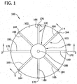
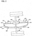
- Figures 1-7 depict an apparatus 100 for mechanically cleaving a bonded structure 102.
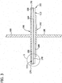
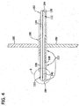
- the bonded structure 102 shown in Figures 1-7 is a bonded wafer pair. However, it should be noted that structures other than a bonded wafer pair may be cleaved by use of the apparatus 100. Referring to Figures 3 and 4 , the structure 102 is separated along a cleave plane 140 shown in phantom.
- the bonded structure 102 has an upper surface 106 (generally, a first surface) and an opposing lower surface 108 (generally, a second surface).
- the bonded structure contains a handle wafer 110 (generally, a first wafer) bonded to a donor wafer 112 (generally, a second wafer) along a bond interface 104.
- the distance between the cleave plane 140 in the donor wafer 112 and the bond interface 104 is exaggerated for the sake of clarity.
- the position of the handle wafer 110 and the donor wafer 112 may be reversed such that the handle wafer is disposed beneath the donor wafer.
- the donor wafer 112 and handle wafer 110 are beveled at their peripheral edge.
- the peripheral edge of the wafers may have a variety of geometries (e.g., rounded, bulleted).
- the term “beveled” refers to a geometry in which the edge is not substantially perpendicular to the front and back surface of the wafer and has one or more tapered edges and should not be considered in a limiting sense.
- a “tapered edge” refers merely to a surface at the wafer edge that is not parallel to the front and back surfaces but rather slopes upward or downward toward the portion of the edge that is most distant from the center of the wafer. Further, such “tapered edges” may be straight or arcuate or may contain both straight and arcuate portions.
- the donor wafer 112 and handle wafer 110 have rounded edges.
- the edge of the donor wafer 112 has a first portion 148 and the edge of the handle wafer 110 has a second portion 152, the first portion being disposed opposite the second portion thereby forming a depression 144 between the two edges.
- the first portion 148 and second portion 152 are tapered edges of the wafer, the edges taping upward or downward depending on the orientation of the bonded wafer pair.
- the donor wafer 112 has a tapered edge 146 (synonymously “upwardly tapered edge”) that slopes upward from the lower surface 108 of the bonded structure toward the portion (or "point” as with rounded edges) 154 of the edge that is most distant from the center of the wafer.
- the donor wafer 112 also includes an edge 148 (synonymously “downwardly tapered edge” or “first portion” as described above) that slopes downward from the interface 104 toward the most outward portion 154 of the edge.
- the handle wafer 110 includes an upwardly tapered edge 152 (or "second portion” as described above) that slopes toward the most outward portion 156 of the edge of the handle wafer and a downwardly tapered edge 150 that tapers to the most outward portion 156 of the edge of the handle wafer 110.
- the downward sloping edge 148 of the donor wafer 112 and the upward sloping edge 152 of the handle wafer 110 form a depression 144 between the two edges.
- the apparatus 100 includes a plurality of first clamps 170 (or “upper clamps”) that releasably secure the handle wafer 110 and a plurality of second clamps 184 that releasably secure the donor wafer 112.
- the clamps 170, 184 are mounted respectively to first arms 160 and second arms 166.
- the first arms 160 extend from a first central disk 190 and the second arms 166 extend from a second central disk 192.
- the first central disk 190 may contact the upper surface 106 of the bonded structure 102 to properly align the first clamps 170 in relation to the structure 102.
- the second central disk 192 may assist in aligning the second clamps 184.
- first clamps 170, first arms 160 and first central disk 190 together form a first grasping member 120 ( Fig. 1 ) and the second clamps 184, second arms 184 and second central disk 192 together form a second grasping member 122 ( Fig 4 ).
- the first grasping member 120 has four arms 160 and four clamps 170 and the second grasping member 122 also has four arms 166 and four clamps 184.
- the apparatus 100 does not have arms but rather annular members for gripping the respective wafers as shown in Figures 8-10 and described below.
- Each first clamp 170 has a surface 130 ( Figures 3 and 5 ) which contacts the upwardly tapered edge 152 of the handle wafer 110.
- each second clamp 184 has a surface 130 ( Figures 4 and 6 ) that contacts the downwardly tapered edge 148 of the donor wafer 112.
- the end portion of the first clamp 170 has a curved profile such that the surface 130 of the arm may enter the depression 144 and contact the upwardly tapered edge 152 of the handle wafer 110 ( Fig. 5 ).
- curved should not be considered limiting and refers to a profile in which the arm generally changes its angular direction relative to other portions of the arm and may include one or more discreet changes in direction (e.g., the arm may form one or more angles within its length).
- the clamp 170 may have a curvature other than 180°.
- the arm 160 may be perpendicular to the front and back surfaces of the bonded structure and the clamp 170 may curve about 90° into the depression 144 to contact its surface 130 with the tapered edge 152.
- the clamp 170 does not have a curved profile such as cases wherein the arm extends from the opposite direction as the arm shown in Figure 7 (i.e., from outside of the bonded structure).
- the second clamp 184 may have a shape and/or dimensions similar to the first clamp 170.
- the second clamp 184 is oriented opposite that of the first clamp 170 to allow the second clamp 184 to grasp the donor wafer 112 (i.e., the clamp 184 curves upward towards the depression 144 ( Figure 5 ) rather than downward).
- the clamps 170, 184 may have other shapes and/or dimensions (e.g., different from each other) without limitation.
- the first clamp 170 converges to form an edge which is the surface 130 which contacts the handle wafer 110 of the bonded structure 102.
- the surface 130 may also have a width (i.e., the surface may be rectangular or square rather than an edge) or may be a singular point which contacts the surface.
- the surface 130 may be arcuate and optionally may have a shape which is complementary to the tapered edge of the handle wafer to increase contact between the handle wafer and the surface 130.
- the surface 130 of the second clamp 184 may have a shape described above in regard to the surface 130 of the first clamp 170.
- the first grasping member 120 and/or the second grasping member 122 grasps that bonded structure.
- the bonded structure 102 may be moved into position by robotic means or by use of one of more of the grasping members 120, 122.
- the other grasping member grasps the structure.
- the bonded structure 102 may be grasped by the first grasping member 120 by extending and retracting one or more of the arms 160 of the member 120 by use of a first actuator (not shown) that forms part of or is attached to the first member 120.
- the bonded structure 102 is grasped by the second grasping member 122 by use of a second actuator (not shown) that is attached to or forms part of the second member 122 to extend and retract one or more arms 166 of the second grasping member 122.
- Actuation of the arms 160, 166 of the first grasping member 120 and second grasping member 122 may be achieved by any method known to those of skill in the art including, for example, pneumatic, hydraulic or mechanical actuation.
- a force is applied to one or both of the first grasping member 120 and second grasping member 122 to separate the bonded structure 102 at the cleave plane 140.
- an actuator (not shown) is attached to the first grasping member 120.
- the actuator causes the first grasping member 120 to apply an upward force to the handle wafer 110 to separate the structure.
- an actuator (the same one or a different actuator) may be attached to the second grasping member 122 that is operable to cause the second grasping member 122 to apply a downward force on the donor wafer 112.
- the actuator(s) may be attached to the shafts 180, 182 or may be attached to other portions of the grasping members 120 or 122. It should be noted that only one of the first grasping member 120 and second grasping member 122 needs to be actuated to provide the force used to separate the bonded structure and the other clamp may be maintained in a stationary position. However, in some embodiments both the first grasping member 120 and second grasping member 122 are actuated.
- the cleaving process may be initiated by use of a blade (not shown) that exerts force on the bonded structure 102.
- the blade is inserting into the depression 144 formed between the handle wafer 110 and donor wafer 112 and exerts force along the bonded structure edge.
- the force results in the initiation of a cleave along the cleave plane 140.
- This cleave in combination with the force exerted by one or both of the grasping members 120, 122 results in the cleaving and separation of the bonded structure along the cleave plane 140.
- the blade is movable in a lateral direction by an actuator (not shown) or other suitable mechanism.
- the grasping member includes one or more annular members which at least partially encompass the bonded structure.
- the first grasping member 120 includes a first annular member 194 and a second annular member 196 to grasp the handle wafer 110 of the bonded structure.
- the second grasping member 122 may also have a first annular member 172 and a second annular member 188 for grasping the donor wafer 112.
- the first annular member 194 and second annular member 196 of the first grasping member 120 each have a surface 130 ( Fig. 10 ) that contacts the first upwardly tapered edge of the handle wafer 110.
- the first annular member 172 and second annular member 188 has a surface 130 that contacts the downwardly tapered edge of the donor wafer 112.
- the annular members 194, 196 are actuated to contact the handle wafer 110 at its edge ( Fig. 9 ).
- the annular members 172, 188 of the second grasping member 122 may be actuated in a similar manner. Once the handle wafer and donor wafer are grasped, the first grasping member 120 and/or second grasping member 122 may be actuated to apply opposing forces and cause the bonded structure to cleave.
- annular members of the first grasping member 120 and second grasping member 122 need not be arranged such that the handle wafer 110 and donor wafer 112 are contacted continuously at their respective peripheral edges.
- the annular members may contact discreet portions of the peripheral edge (i.e., the annular members may have a length less than half the circumference of the bonded structure when the grasping member has two annular members).
- each grasping member may have more than two annular members without limitation.
- one or both of the grasping members are composed of one annular member (i.e., the grasping member is a continuous annulus) that has an actuated edge that allows the grasping member to change diameter to allow the donor and/or handle wafer to be grasped and released after cleaving.
- An exemplary grasping member 120 is shown in Figure 11 .
- the grasping member 120 includes an actuated lip 176 which may have one or more actuated portions 108 which change the inner diameter D of the grasping member upon actuation.
- the grasping member moves axially with respect to the bonded structure to grasp the bonded structure (i.e., approaches the bonded structure from above or below the structure) rather than moving radially as with the grasping members 120, 122 shown in Figures 8-10 .
- Example 1 Comparison of the ACCUMAP® Image of a SOI Structure Cleaved by use of Suction Cups and a SOI Structure Cleaved by Applying Opposing Forces at the Wafer Edge
- a bonded wafer pair was cleaved by a conventional process that used suction cups to separate the donor wafer from the resulting SOI structure.
- the cleave was initiated by use of a cleave blade.
- a second SOI structure was also prepared by applying an upward and downward force to the bonded structure after the cleave was initiated by the cleave blade.
- the surface of the device layer was imaged to produce an ACCUMAP® image (ACCUMAP® 3220; ADE).
- the image produced from the SOI structure cleaved by the conventional method that used suction cups is shown in Figure 12 and the image produced from the SOI structure cleaved by applying opposite forces at the bonded wafer edge is shown in Figure 13 .
- the SOI structure produced by using suction cups during the cleave had strong cleave striations at the bottom, far left and far right of the image.
- the SOI structure of Figure 13 is more symmetrical and results in greater thickness uniformity.
Description
- This disclosure generally relates to apparatus and methods for cleaving a bonded wafer structure and, more particularly, to apparatus and methods that involve clamps that are actuated to cause the bonded structure to cleave.
- Semiconductor wafers are generally prepared from a single crystal ingot (e.g., a silicon ingot) which is sliced into wafers. The wafers are ground and/or polished to produce product wafers. While reference will be made herein to semiconductor wafers constructed from silicon, other materials may be used as well, such as germanium or gallium arsenide.
- One type of wafer is a silicon-on-insulator (SOI) wafer. An SOI wafer includes a thin layer of silicon atop an insulating layer (e.g., an oxide layer), which is in turn disposed on a silicon substrate.
- An exemplary process of making an SOI wafer includes depositing a layer of oxide on a polished front surface of a donor wafer and/or a handle wafer. Particles (e.g., hydrogen atoms or a combination of hydrogen and helium atoms) are implanted at a specified depth beneath the front surface of the donor wafer. The implanted particles form a cleave plane in the donor wafer at the specified depth at which they were implanted. The surface of the donor wafer is cleaned to remove organic compounds deposited on the wafer during the implantation process.
- The front surface of the donor wafer is then bonded to a handle wafer to form a bonded wafer pair through a hydrophilic bonding process. The donor wafer and handle wafer are bonded together by exposing the surfaces of the wafers to plasma containing, for example, oxygen or nitrogen. Exposure to the plasma modifies the structure of the surfaces in a process often referred to as surface activation. The wafers are then pressed together and a bond is formed therebetween. This bond is relatively weak, and must be strengthened before further processing can occur.
- In some processes, the hydrophilic bond between the donor wafer and handle wafer (i.e., a bonded wafer) is strengthened by heating or annealing the bonded wafer pair at temperatures between approximately 300°C and 500°C. The elevated temperatures cause the formation of covalent bonds between the adjoining surfaces of the donor wafer and the handle wafer, thus solidifying the bond between the donor wafer and the handle wafer. Concurrently with the heating or annealing of the bonded wafer, the particles earlier implanted in the donor wafer weaken the cleave plane. A portion of the donor wafer is then separated (i.e., cleaved) along the cleave plane from the bonded wafer pair to form the SOI wafer.
- The bonded wafer is first placed in a fixture in which mechanical force is applied perpendicular to the opposing sides of the bonded wafer in order to pull a portion of the donor wafer apart from the bonded wafer. According to some methods, suction cups are utilized to apply the mechanical force. The separation of the portion of the donor wafer is initiated by applying a mechanical wedge at the edge of the bonded wafer at the interface between the donor wafer and the handle wafer. The application of the mechanical force initiates propagation of a cleave along the cleave plane. The mechanical force applied by the suction cups then pulls a portion of the donor wafer away from the bonded wafer, thus forming an SOI wafer.
- The resulting SOI wafer thus comprises a thin layer of silicon disposed atop the oxide layer and the handle wafer: The thickness of the layer may be non-uniform. The layer may also have a non-uniform roughness. This non-uniform thickness and roughness of the layer may be the result of the cleave propagating at varying speeds and/or the mechanical force applied by the suction cups. Additional processing is thus required to reduce the variation in thickness of the layer and/or smooth this layer. These additional processing steps are both time consuming and costly.
-
EP 1178521 discloses an apparatus for separating a bonded substrate stack. - Thus, there remains a continuing need for a system and method for cleaving a bonded wafer structure that results in the structure having a layer with a relatively uniform thickness and roughness.
- This Background section is intended to introduce the reader to various aspects of art that may be related to various aspects of the present disclosure, which are described and/or claimed below. This discussion is believed to be helpful in providing the reader with background information to facilitate a better understanding of the various aspects of the present disclosure.
- One aspect of the present disclosure is directed to an apparatus for cleaving a bonded wafer structure that includes a first wafer and a second wafer. The first wafer has a peripheral edge that includes a first portion and the second wafer has a peripheral edge that includes a second portion. The first portion is disposed opposite the second portion. The apparatus includes a first grasping member and a second grasping member. The first grasping member has one or more annular members. The annular members have a surface for contacting the first portion of the peripheral edge of the first wafer. The second grasping member has one or more annular members. The annular members have a surface for contacting the second portion of the peripheral edge of the second wafer. The one or more annular members of the first grasping member or the one or more annular members of the second grasping member have an actuated edge for grasping and releasing the wafer. An actuator is attached to the first grasping member. The first grasping member applies a force to the first wafer to cleave the bonded wafer structure upon activation of the actuator.
- Another aspect of the present disclosure is directed to a method of cleaving a bonded wafer structure that includes a first wafer and a second wafer. The first wafer has a peripheral edge that includes a first portion and the second wafer has a peripheral edge that includes a second portion. The first portion is disposed opposite the second portion. The first portion of the peripheral edge of the first wafer is contacted with a surface of an annular member of a first grasping member. The second portion of the peripheral edge of the second wafer is contacted with a surface of an annular member of a second grasping member. The annular member of the first grasping member or the annular member of the second grasping member has an actuated edge. The actuated edge is actuated to grasp the first wafer or the second wafer. The bonded wafer structure is cleaved by at least one of (1) applying an upward force on the first wafer by actuating the first grasping member upward or (2) applying a downward force on the second wafer by actuating the second grasping member downward.
- Various refinements exist of the features noted in relation to the above-mentioned aspects of the present disclosure. Further features may also be incorporated in the above-mentioned aspects of the present disclosure as well. These refinements and additional features may exist individually or in any combination. For instance, various features discussed below in relation to any of the illustrated embodiments of the present disclosure may be incorporated into any of the above-described aspects of the present disclosure, alone or in any combination.
-
-
Figure 1 is a top view of an apparatus for cleaving a bonded wafer structure; -
Figure 2 is a perspective view of the apparatus ofFigure 1 ; -
Figure 3 is a cross-sectional view ofFigure 1 taken along the 3--3 line showing the apparatus prior to cleaving the bonded wafer structure; -
Figure 4 is a cross-sectional view ofFigure 1 taken along the 4-4 line showing the apparatus prior to cleaving the bonded wafer structure; -
Figure 5 is an enlarged portion ofFigure 3 ; -
Figure 6 is an enlarged portion ofFigure 4 ; -
Figure 7 is a perspective view of a clamp used in an apparatus for cleaving a bonded wafer structure; -
Figure 8 is a top view of an apparatus used for cleaving a bonded wafer structure before securing the structure; -
Figure 9 is a top view of an apparatus used for cleaving a bonded wafer structure after securing the structure; -
Figure 10 is a cross-sectional view of Figure taken along line 10-10; -
Figure 11 is a top view of an apparatus for cleaving a bonded wafer; -
Figure 12 is black and white ACCUMAP® image of a surface of a SOI wafer after cleaving by a conventional process using suction cups; and -
Figure 13 is black and white ACUMAP® image of a surface of a SOI wafer after cleaving by a process in which opposite forces are applied at the bonded wafer edge. - Corresponding reference characters indicate corresponding parts throughout the drawings.
- The embodiments described herein generally relate to apparatus and methods for mechanically cleaving a bonded wafer structure such as a bonded wafer pair. The apparatus and methods cleave (i.e., separate) the bonded structure along a cleave plane within the structure to form a new structure such as a silicon-on-insulator (SOI) wafer. While reference is made herein to use of the apparatus and methods to form silicon-on-insulator structures, the systems and methods can also be used to form other structures without limitation.
-
Figures 1-7 depict anapparatus 100 for mechanically cleaving a bondedstructure 102. The bondedstructure 102 shown inFigures 1-7 is a bonded wafer pair. However, it should be noted that structures other than a bonded wafer pair may be cleaved by use of theapparatus 100. Referring toFigures 3 and4 , thestructure 102 is separated along acleave plane 140 shown in phantom. The bondedstructure 102 has an upper surface 106 (generally, a first surface) and an opposing lower surface 108 (generally, a second surface). The bonded structure contains a handle wafer 110 (generally, a first wafer) bonded to a donor wafer 112 (generally, a second wafer) along abond interface 104. The distance between thecleave plane 140 in thedonor wafer 112 and thebond interface 104 is exaggerated for the sake of clarity. Furthermore, in other embodiments, the position of thehandle wafer 110 and thedonor wafer 112 may be reversed such that the handle wafer is disposed beneath the donor wafer. - As shown in
Figures 5 and6 , thedonor wafer 112 and handlewafer 110 are beveled at their peripheral edge. It should be noted that the peripheral edge of the wafers may have a variety of geometries (e.g., rounded, bulleted). As used herein, the term "beveled" refers to a geometry in which the edge is not substantially perpendicular to the front and back surface of the wafer and has one or more tapered edges and should not be considered in a limiting sense. Further, it should be noted that, as used herein a "tapered edge" refers merely to a surface at the wafer edge that is not parallel to the front and back surfaces but rather slopes upward or downward toward the portion of the edge that is most distant from the center of the wafer. Further, such "tapered edges" may be straight or arcuate or may contain both straight and arcuate portions. - As also shown in
Figures 5 and6 , thedonor wafer 112 and handlewafer 110 have rounded edges. The edge of thedonor wafer 112 has afirst portion 148 and the edge of thehandle wafer 110 has asecond portion 152, the first portion being disposed opposite the second portion thereby forming adepression 144 between the two edges. Generally thefirst portion 148 andsecond portion 152 are tapered edges of the wafer, the edges taping upward or downward depending on the orientation of the bonded wafer pair. As shown inFigure 5 and6 , thedonor wafer 112 has a tapered edge 146 (synonymously "upwardly tapered edge") that slopes upward from thelower surface 108 of the bonded structure toward the portion (or "point" as with rounded edges) 154 of the edge that is most distant from the center of the wafer. Thedonor wafer 112 also includes an edge 148 (synonymously "downwardly tapered edge" or "first portion" as described above) that slopes downward from theinterface 104 toward the mostoutward portion 154 of the edge. Similar to thedonor wafer 112, thehandle wafer 110 includes an upwardly tapered edge 152 (or "second portion" as described above) that slopes toward the mostoutward portion 156 of the edge of the handle wafer and a downwardly taperededge 150 that tapers to the mostoutward portion 156 of the edge of thehandle wafer 110. The downwardsloping edge 148 of thedonor wafer 112 and the upwardsloping edge 152 of thehandle wafer 110 form adepression 144 between the two edges. - As shown in
Figures 1-4 , theapparatus 100 includes a plurality of first clamps 170 (or "upper clamps") that releasably secure thehandle wafer 110 and a plurality ofsecond clamps 184 that releasably secure thedonor wafer 112. Theclamps first arms 160 andsecond arms 166. Thefirst arms 160 extend from a firstcentral disk 190 and thesecond arms 166 extend from a secondcentral disk 192. The firstcentral disk 190 may contact theupper surface 106 of the bondedstructure 102 to properly align thefirst clamps 170 in relation to thestructure 102. Similarly, the secondcentral disk 192 may assist in aligning thesecond clamps 184. The first clamps 170,first arms 160 and firstcentral disk 190 together form a first grasping member 120 (Fig. 1 ) and thesecond clamps 184,second arms 184 and secondcentral disk 192 together form a second grasping member 122 (Fig 4 ). - As shown in
Figure 1 , the first graspingmember 120 has fourarms 160 and fourclamps 170 and the second graspingmember 122 also has fourarms 166 and fourclamps 184. However, in embodiments of the invention, theapparatus 100 does not have arms but rather annular members for gripping the respective wafers as shown inFigures 8-10 and described below. - Each
first clamp 170 has a surface 130 (Figures 3 and5 ) which contacts the upwardlytapered edge 152 of thehandle wafer 110. Similarly, eachsecond clamp 184 has a surface 130 (Figures 4 and6 ) that contacts the downwardly taperededge 148 of thedonor wafer 112. As shown in further detail inFigure 7 , the end portion of thefirst clamp 170 has a curved profile such that thesurface 130 of the arm may enter thedepression 144 and contact the upwardlytapered edge 152 of the handle wafer 110 (Fig. 5 ). In this regard, the term "curved" should not be considered limiting and refers to a profile in which the arm generally changes its angular direction relative to other portions of the arm and may include one or more discreet changes in direction (e.g., the arm may form one or more angles within its length). - It should be noted that while the
first clamp 170 is shown with a curvature of 180°, in other cases wherein the arm does not extend from the center of the bonded structure, the clamp may have a curvature other than 180°. For example, thearm 160 may be perpendicular to the front and back surfaces of the bonded structure and theclamp 170 may curve about 90° into thedepression 144 to contact itssurface 130 with thetapered edge 152. In some cases, theclamp 170 does not have a curved profile such as cases wherein the arm extends from the opposite direction as the arm shown inFigure 7 (i.e., from outside of the bonded structure). In this regard, thesecond clamp 184 may have a shape and/or dimensions similar to thefirst clamp 170. However, thesecond clamp 184 is oriented opposite that of thefirst clamp 170 to allow thesecond clamp 184 to grasp the donor wafer 112 (i.e., theclamp 184 curves upward towards the depression 144 (Figure 5 ) rather than downward). Theclamps - As shown in
Figure 7 , thefirst clamp 170 converges to form an edge which is thesurface 130 which contacts thehandle wafer 110 of the bondedstructure 102. However, thesurface 130 may also have a width (i.e., the surface may be rectangular or square rather than an edge) or may be a singular point which contacts the surface. Further, thesurface 130 may be arcuate and optionally may have a shape which is complementary to the tapered edge of the handle wafer to increase contact between the handle wafer and thesurface 130. Thesurface 130 of thesecond clamp 184 may have a shape described above in regard to thesurface 130 of thefirst clamp 170. - To separate the bonded
structure 102, the first graspingmember 120 and/or the second graspingmember 122 grasps that bonded structure. Before being grasped, the bondedstructure 102 may be moved into position by robotic means or by use of one of more of the graspingmembers structure 102 may be grasped by the first graspingmember 120 by extending and retracting one or more of thearms 160 of themember 120 by use of a first actuator (not shown) that forms part of or is attached to thefirst member 120. Similarly, the bondedstructure 102 is grasped by the second graspingmember 122 by use of a second actuator (not shown) that is attached to or forms part of thesecond member 122 to extend and retract one ormore arms 166 of the second graspingmember 122. Actuation of thearms member 120 and second graspingmember 122 may be achieved by any method known to those of skill in the art including, for example, pneumatic, hydraulic or mechanical actuation. - After the bonded
structure 102 is grasped by the first graspingmember 120 and the second graspingmember 122, a force is applied to one or both of the first graspingmember 120 and second graspingmember 122 to separate the bondedstructure 102 at thecleave plane 140. In this regard, an actuator (not shown) is attached to the first graspingmember 120. The actuator causes the first graspingmember 120 to apply an upward force to thehandle wafer 110 to separate the structure. Additionally, an actuator (the same one or a different actuator) may be attached to the second graspingmember 122 that is operable to cause the second graspingmember 122 to apply a downward force on thedonor wafer 112. The actuator(s) may be attached to theshafts 180, 182 or may be attached to other portions of the graspingmembers member 120 and second graspingmember 122 needs to be actuated to provide the force used to separate the bonded structure and the other clamp may be maintained in a stationary position. However, in some embodiments both the first graspingmember 120 and second graspingmember 122 are actuated. - The cleaving process may be initiated by use of a blade (not shown) that exerts force on the bonded
structure 102. The blade is inserting into thedepression 144 formed between thehandle wafer 110 anddonor wafer 112 and exerts force along the bonded structure edge. The force results in the initiation of a cleave along thecleave plane 140. This cleave in combination with the force exerted by one or both of the graspingmembers cleave plane 140. The blade is movable in a lateral direction by an actuator (not shown) or other suitable mechanism. - In embodiments of the present disclosure and as shown in
Figures 8-10 , rather than having a plurality of arms, the grasping member includes one or more annular members which at least partially encompass the bonded structure. As shown inFigure 8 , the first graspingmember 120 includes a firstannular member 194 and a secondannular member 196 to grasp thehandle wafer 110 of the bonded structure. The second grasping member 122 (Fig. 10 ) may also have a firstannular member 172 and a secondannular member 188 for grasping thedonor wafer 112. - The first
annular member 194 and secondannular member 196 of the first graspingmember 120 each have a surface 130 (Fig. 10 ) that contacts the first upwardly tapered edge of thehandle wafer 110. Similarly, the firstannular member 172 and secondannular member 188 has asurface 130 that contacts the downwardly tapered edge of thedonor wafer 112. As indicated by arrows inFigure 8 , theannular members handle wafer 110 at its edge (Fig. 9 ). Theannular members member 122 may be actuated in a similar manner. Once the handle wafer and donor wafer are grasped, the first graspingmember 120 and/or second graspingmember 122 may be actuated to apply opposing forces and cause the bonded structure to cleave. - It should be noted that the annular members of the first grasping
member 120 and second graspingmember 122 need not be arranged such that thehandle wafer 110 anddonor wafer 112 are contacted continuously at their respective peripheral edges. The annular members may contact discreet portions of the peripheral edge (i.e., the annular members may have a length less than half the circumference of the bonded structure when the grasping member has two annular members). Further, each grasping member may have more than two annular members without limitation. - In some embodiments, one or both of the grasping members are composed of one annular member (i.e., the grasping member is a continuous annulus) that has an actuated edge that allows the grasping member to change diameter to allow the donor and/or handle wafer to be grasped and released after cleaving. An exemplary grasping
member 120 is shown inFigure 11 . The graspingmember 120 includes an actuatedlip 176 which may have one or moreactuated portions 108 which change the inner diameter D of the grasping member upon actuation. The grasping member moves axially with respect to the bonded structure to grasp the bonded structure (i.e., approaches the bonded structure from above or below the structure) rather than moving radially as with the graspingmembers Figures 8-10 . - Without being held to any particular theory, it is believed that non-uniform thickness and/or roughness variations in the layers of structures (e.g., SOI structures) produced according to previous systems were caused by localized stress applied to the surface of the bonded structure. The embodiments described herein reduce or eliminate this problem by applying force at the wafer edge thereby reducing or eliminating thickness and/or roughness variations in the resulting device layer.
- The processes of the present disclosure are further illustrated by the following Examples. These Examples should not be viewed in a limiting sense.
- A bonded wafer pair was cleaved by a conventional process that used suction cups to separate the donor wafer from the resulting SOI structure. The cleave was initiated by use of a cleave blade. A second SOI structure was also prepared by applying an upward and downward force to the bonded structure after the cleave was initiated by the cleave blade.
- After the wafer was cleaved to produce the SOI structures, the surface of the device layer was imaged to produce an ACCUMAP® image (ACCUMAP® 3220; ADE). The image produced from the SOI structure cleaved by the conventional method that used suction cups is shown in
Figure 12 and the image produced from the SOI structure cleaved by applying opposite forces at the bonded wafer edge is shown inFigure 13 . As can be seen fromFigure 12 , the SOI structure produced by using suction cups during the cleave had strong cleave striations at the bottom, far left and far right of the image. The SOI structure ofFigure 13 is more symmetrical and results in greater thickness uniformity. - When introducing elements of the present disclosure or the embodiment(s) thereof, the articles "a", "an", "the" and "said" are intended to mean that there are one or more of the elements. The terms "comprising," "including," "containing" and "having" are intended to be inclusive and mean that there may be additional elements other than the listed elements. The use of terms indicating a particular orientation (e.g., "top", "bottom", "side", etc.) is for convenience of description and does not require any particular orientation of the item described.
- Various changes could be made in the above constructions and methods without departing from the scope of the disclosure.
- The scope of the invention is defined in the appended claims.
Claims (12)
- An apparatus (100) for cleaving a bonded wafer structure (102) comprising a first wafer (110) and a second wafer (112), the first wafer having a peripheral edge including a first portion (148), the second wafer having a peripheral edge including a second portion (152), the first portion disposed opposite the second portion, the apparatus comprising:a first grasping member (120) having one or more annular members (194)(196), the one or more annular members having a surface (130) for contacting the first portion of the peripheral edge of the first wafer; anda second grasping member (122) having one or more annular members (172)(188), the one or more annular members having a surface (130) for contacting the second portion of the peripheral edge of the second wafer, wherein the one or more annular members of the first grasping member or the one or more annular members of the second grasping member have an actuated edge for grasping and releasing the wafer;the apparatus being characterized in that it further comprises an actuator attached to the first grasping member, the first grasping member applying a force to the first wafer to cleave the bonded wafer structure upon activation of the actuator.
- The apparatus (100) as set forth in claim 1 wherein the one or more annular members (194)(196) of the first grasping member (120) continuously contact the first portion (148) of the peripheral edge of the first wafer (110).
- The apparatus as set forth in claim 1 or claim 2 wherein the one or more annular members (172)(188) of the second grasping member (122) continuously contact the second portion (152) of the peripheral edge of the second wafer (112).
- The apparatus (100) as set forth in any one of claims 1 to 3 wherein the first grasping member (120) comprises only one annular member (194), the annular member of the first grasping member having an actuated edge for grasping and releasing the first wafer (110), and wherein the second grasping member (122) comprises only one annular member (172), the annular member of the second grasping member having an actuated edge for grasping and releasing the second wafer (112).
- The apparatus (100) as set forth in any one of claims 1 to 4 further comprising an actuator attached to the second grasping member (122), the second grasping member applying a force to the second wafer (112) to cleave the bonded wafer structure upon activation of the actuator, wherein the forces applied by the first and second grasping member are opposing forces.
- A method of cleaving a bonded wafer structure comprising a first wafer (110) and a second wafer (112), the first wafer having a peripheral edge including a first portion (148), the second wafer having a peripheral edge including a second portion (152), the first portion disposed opposite the second portion, the method comprising:contacting the first portion of the peripheral edge of the first wafer with a surface of an annular member (194) of a first grasping member (120);contacting the second portion of the peripheral edge of the second wafer with a surface of an annular member (172) of a second grasping member (122), wherein the annular member of the first grasping member or the annular member of the second grasping member has an actuated edge; andactuating the actuated edge to grasp the first wafer or the second wafer;the method being characterized in that it further comprises cleaving the bonded wafer structure by at least one of (1) applying a force on the first wafer by actuating the first grasping member or (2) applying a force on the second wafer by actuating the second grasping member.
- The method as set forth in claim 6 further comprising inserting a blade between the first wafer (110) and the second wafer (112) to initiate cleaving of the bonded wafer pair.
- The method as set forth in claim 6 or claim 7 comprising actuating the first grasping member (120) to apply a force to the first wafer (110) and actuating the second grasping member (122) to apply an opposing force to the second wafer (112) to cleave the bonded wafer structure.
- The method as set forth in any one of claims 6 to 8 wherein one or more annular members (194)(196) of the first grasping member (120) continuously contact the first portion (148) of the peripheral edge of the first wafer (110).
- The method as set forth in any one of claims 6 to 9 wherein one or more annular members (172)(188) of the second grasping member (122) continuously contact the second portion (152) of the peripheral edge of the second wafer (112).
- The method as set forth in any one of claims 6 to 10 wherein the first grasping member (120) comprises only one annular member (194), the annular member having an actuated edge, the method comprising actuating the edge to grasp and release the first wafer (110).
- The method as set forth in any one of claims 6 to 11 wherein the second grasping member (122) comprises only one annular member (172), the annular member having an actuated edge, the method comprising actuating the edge to grasp and release the second wafer (112).
Applications Claiming Priority (2)
| Application Number | Priority Date | Filing Date | Title |
|---|---|---|---|
| US201161553447P | 2011-10-31 | 2011-10-31 | |
| PCT/US2012/062194 WO2013066758A1 (en) | 2011-10-31 | 2012-10-26 | Clamping apparatus for cleaving a bonded wafer structure and methods for cleaving |
Publications (2)
| Publication Number | Publication Date |
|---|---|
| EP2774176A1 EP2774176A1 (en) | 2014-09-10 |
| EP2774176B1 true EP2774176B1 (en) | 2016-08-10 |
Family
ID=47221551
Family Applications (1)
| Application Number | Title | Priority Date | Filing Date |
|---|---|---|---|
| EP12790726.9A Active EP2774176B1 (en) | 2011-10-31 | 2012-10-26 | Clamping apparatus for cleaving a bonded wafer structure and methods for cleaving |
Country Status (7)
| Country | Link |
|---|---|
| US (3) | US9159596B2 (en) |
| EP (1) | EP2774176B1 (en) |
| JP (1) | JP6167108B2 (en) |
| KR (1) | KR102061359B1 (en) |
| CN (1) | CN104025277A (en) |
| TW (1) | TWI622119B (en) |
| WO (1) | WO2013066758A1 (en) |
Families Citing this family (13)
| Publication number | Priority date | Publication date | Assignee | Title |
|---|---|---|---|---|
| KR102061359B1 (en) | 2011-10-31 | 2019-12-31 | 글로벌웨이퍼스 씨오., 엘티디. | Clamping apparatus for cleaving a bonded wafer structure and methods for cleaving |
| US9922862B2 (en) * | 2014-01-28 | 2018-03-20 | Ev Group E. Thallner Gmbh | Device and method for loosening a first substrate |
| CN104505363A (en) * | 2014-12-25 | 2015-04-08 | 苏州凯锝微电子有限公司 | Wafer clamping device |
| CN104701233B (en) * | 2015-03-10 | 2017-10-17 | 北京七星华创电子股份有限公司 | A kind of disk clamping device |
| KR101950157B1 (en) * | 2015-08-11 | 2019-02-19 | 도오꾜오까고오교 가부시끼가이샤 | Support Separation Device and Support Separation Method |
| US10272661B2 (en) * | 2017-04-17 | 2019-04-30 | Taiwan Semiconductor Manufacturing Company, Ltd. | Pad removal device and method |
| EP3657537A1 (en) * | 2018-11-23 | 2020-05-27 | ATOTECH Deutschland GmbH | End effector for slab formed substrates |
| FR3093715B1 (en) * | 2019-03-15 | 2021-03-05 | Soitec Silicon On Insulator | Holding device for an assembly to be fractured |
| FR3093858B1 (en) * | 2019-03-15 | 2021-03-05 | Soitec Silicon On Insulator | Method of transferring a useful layer onto a support substrate |
| CN110640324B (en) * | 2019-09-02 | 2022-06-10 | 中芯集成电路(宁波)有限公司 | Wafer double-side manufacturing system |
| JP7309191B2 (en) * | 2019-11-06 | 2023-07-18 | 中村留精密工業株式会社 | Wafer splitter |
| US11855036B2 (en) | 2020-02-27 | 2023-12-26 | Kioxia Corporation | Bonding apparatus and bonding method |
| JP7339905B2 (en) | 2020-03-13 | 2023-09-06 | キオクシア株式会社 | Bonding device and bonding method |
Citations (1)
| Publication number | Priority date | Publication date | Assignee | Title |
|---|---|---|---|---|
| EP1178521A2 (en) * | 2000-07-31 | 2002-02-06 | Canon Kabushiki Kaisha | Method and apparatus for processing composite member |
Family Cites Families (31)
| Publication number | Priority date | Publication date | Assignee | Title |
|---|---|---|---|---|
| SE369160B (en) * | 1972-12-21 | 1974-08-12 | Siporex Int Ab | |
| US5367762A (en) * | 1992-12-23 | 1994-11-29 | Advanced Micro Devices, Inc. | Decapping machine for packaged integrated circuits |
| JP3408000B2 (en) * | 1994-11-28 | 2003-05-19 | 菱電セミコンダクタシステムエンジニアリング株式会社 | Pellicle peeling method |
| JPH09263500A (en) | 1996-01-22 | 1997-10-07 | Komatsu Electron Metals Co Ltd | Jig for stripping stuck soi wafer |
| US6162705A (en) | 1997-05-12 | 2000-12-19 | Silicon Genesis Corporation | Controlled cleavage process and resulting device using beta annealing |
| JPH115064A (en) * | 1997-06-16 | 1999-01-12 | Canon Inc | Separation device for sample and method thereof and production of board |
| EP0951068A1 (en) * | 1998-04-17 | 1999-10-20 | Interuniversitair Micro-Elektronica Centrum Vzw | Method of fabrication of a microstructure having an inside cavity |
| US6672358B2 (en) | 1998-11-06 | 2004-01-06 | Canon Kabushiki Kaisha | Sample processing system |
| JP3917313B2 (en) * | 1999-01-26 | 2007-05-23 | ローム株式会社 | Transfer jig for semiconductor manufacturing products |
| US6221740B1 (en) | 1999-08-10 | 2001-04-24 | Silicon Genesis Corporation | Substrate cleaving tool and method |
| US6263941B1 (en) | 1999-08-10 | 2001-07-24 | Silicon Genesis Corporation | Nozzle for cleaving substrates |
| EP1939932A1 (en) | 1999-08-10 | 2008-07-02 | Silicon Genesis Corporation | A substrate comprising a stressed silicon germanium cleave layer |
| US6336787B1 (en) | 1999-10-07 | 2002-01-08 | Mosel Vitelic, Inc. | Method for transferring wafers in a semiconductor tape-peeling apparatus |
| TW508690B (en) | 1999-12-08 | 2002-11-01 | Canon Kk | Composite member separating method, thin film manufacturing method, and composite member separating apparatus |
| US6444082B1 (en) | 2000-06-22 | 2002-09-03 | International Business Machines Corporation | Apparatus and method for removing a bonded lid from a substrate |
| US6491083B2 (en) | 2001-02-06 | 2002-12-10 | Anadigics, Inc. | Wafer demount receptacle for separation of thinned wafer from mounting carrier |
| FR2823373B1 (en) | 2001-04-10 | 2005-02-04 | Soitec Silicon On Insulator | DEVICE FOR CUTTING LAYER OF SUBSTRATE, AND ASSOCIATED METHOD |
| AT502233B1 (en) | 2001-06-07 | 2007-04-15 | Thallner Erich | Carrier detachment device aligns inner, near-edge surface of frame with semiconductor disk and bonds them to foil, before detaching disk from carrier |
| JP2003288028A (en) | 2001-12-25 | 2003-10-10 | Canon Inc | Method for disassembling image display apparatus, method for producing image display apparatus, method for producing support member, method for producing image display unit, method for producing working material, and image display apparatus |
| FR2834381B1 (en) * | 2002-01-03 | 2004-02-27 | Soitec Silicon On Insulator | DEVICE FOR CUTTING A LAYER OF A SUBSTRATE, AND ASSOCIATED METHOD |
| TWI223371B (en) * | 2003-03-18 | 2004-11-01 | Taiwan Semiconductor Mfg | Chuck rotating and chuck roller apparatuses |
| JP4364535B2 (en) | 2003-03-27 | 2009-11-18 | シャープ株式会社 | Manufacturing method of semiconductor device |
| WO2005024916A1 (en) | 2003-09-05 | 2005-03-17 | Sumco Corporation | Method for producing soi wafer |
| JP2006135272A (en) | 2003-12-01 | 2006-05-25 | Tokyo Ohka Kogyo Co Ltd | Substrate support plate and peeling method of support plate |
| JP4995626B2 (en) * | 2007-04-27 | 2012-08-08 | 信越化学工業株式会社 | Manufacturing method of bonded substrate |
| JP2009154407A (en) | 2007-12-27 | 2009-07-16 | Tdk Corp | Peeling apparatus, peeling method, and information recording medium manufacturing method |
| JP2010010207A (en) * | 2008-06-24 | 2010-01-14 | Tokyo Ohka Kogyo Co Ltd | Separating apparatus and separating method |
| JP5448860B2 (en) * | 2010-01-13 | 2014-03-19 | 東京応化工業株式会社 | Separation method and separation apparatus |
| US8845859B2 (en) | 2011-03-15 | 2014-09-30 | Sunedison Semiconductor Limited (Uen201334164H) | Systems and methods for cleaving a bonded wafer pair |
| KR102061359B1 (en) * | 2011-10-31 | 2019-12-31 | 글로벌웨이퍼스 씨오., 엘티디. | Clamping apparatus for cleaving a bonded wafer structure and methods for cleaving |
| US9806054B2 (en) * | 2011-12-22 | 2017-10-31 | Ev Group E. Thallner Gmbh | Flexible substrate holder, device and method for detaching a first substrate |
-
2012
- 2012-10-26 KR KR1020147011610A patent/KR102061359B1/en active IP Right Grant
- 2012-10-26 CN CN201280053782.4A patent/CN104025277A/en active Pending
- 2012-10-26 EP EP12790726.9A patent/EP2774176B1/en active Active
- 2012-10-26 JP JP2014539062A patent/JP6167108B2/en active Active
- 2012-10-26 WO PCT/US2012/062194 patent/WO2013066758A1/en active Application Filing
- 2012-10-29 US US13/663,073 patent/US9159596B2/en active Active
- 2012-10-29 US US13/663,038 patent/US9165802B2/en active Active
- 2012-10-31 TW TW101140405A patent/TWI622119B/en active
-
2015
- 2015-09-04 US US14/845,327 patent/US9925755B2/en active Active
Patent Citations (1)
| Publication number | Priority date | Publication date | Assignee | Title |
|---|---|---|---|---|
| EP1178521A2 (en) * | 2000-07-31 | 2002-02-06 | Canon Kabushiki Kaisha | Method and apparatus for processing composite member |
Also Published As
| Publication number | Publication date |
|---|---|
| EP2774176A1 (en) | 2014-09-10 |
| TW201324676A (en) | 2013-06-16 |
| US20130105538A1 (en) | 2013-05-02 |
| WO2013066758A1 (en) | 2013-05-10 |
| TWI622119B (en) | 2018-04-21 |
| CN104025277A (en) | 2014-09-03 |
| US9159596B2 (en) | 2015-10-13 |
| US20150375495A1 (en) | 2015-12-31 |
| US20130105539A1 (en) | 2013-05-02 |
| KR20140085477A (en) | 2014-07-07 |
| US9925755B2 (en) | 2018-03-27 |
| JP2014532992A (en) | 2014-12-08 |
| KR102061359B1 (en) | 2019-12-31 |
| US9165802B2 (en) | 2015-10-20 |
| JP6167108B2 (en) | 2017-07-19 |
Similar Documents
| Publication | Publication Date | Title |
|---|---|---|
| EP2774176B1 (en) | Clamping apparatus for cleaving a bonded wafer structure and methods for cleaving | |
| US8845859B2 (en) | Systems and methods for cleaving a bonded wafer pair | |
| US6468879B1 (en) | Method and device for separating a plate of material, in particular semiconductor material, into two wafers | |
| KR101299719B1 (en) | Process for fabricating a multilayer structure with trimming using thermo-mechanical effects | |
| TWI428956B (en) | Substrate stiffness method and resulting devices for layer transfer processes | |
| US8158487B2 (en) | Annealing process for annealing a structure | |
| KR20110115570A (en) | Method for processing a silicon-on-insulator structure | |
| US7264996B2 (en) | Method for separating wafers bonded together to form a stacked structure | |
| TW202403938A (en) | Cleave systems having spring members for cleaving a semiconductor structure and methods for cleaving such structures | |
| KR101787552B1 (en) | Methods for processing silicon on insulator wafers | |
| KR20120099923A (en) | Preparing method of graphene substrate and graphene substrate by the same | |
| WO2014049414A1 (en) | Direct bonding process | |
| FI129855B (en) | Method and structure for thin-film fabrication | |
| TWI833039B (en) | Cleave systems having spring members for cleaving a semiconductor structure and methods for cleaving such structures | |
| EP3772747B1 (en) | Positioning tool | |
| TW201935519A (en) | Detachable structure and detachment process using said structure |
Legal Events
| Date | Code | Title | Description |
|---|---|---|---|
| PUAI | Public reference made under article 153(3) epc to a published international application that has entered the european phase |
Free format text: ORIGINAL CODE: 0009012 |
|
| 17P | Request for examination filed |
Effective date: 20140411 |
|
| AK | Designated contracting states |
Kind code of ref document: A1 Designated state(s): AL AT BE BG CH CY CZ DE DK EE ES FI FR GB GR HR HU IE IS IT LI LT LU LV MC MK MT NL NO PL PT RO RS SE SI SK SM TR |
|
| DAX | Request for extension of the european patent (deleted) | ||
| 17Q | First examination report despatched |
Effective date: 20150424 |
|
| GRAP | Despatch of communication of intention to grant a patent |
Free format text: ORIGINAL CODE: EPIDOSNIGR1 |
|
| RIC1 | Information provided on ipc code assigned before grant |
Ipc: H01L 21/67 20060101AFI20150921BHEP Ipc: B32B 43/00 20060101ALI20150921BHEP |
|
| INTG | Intention to grant announced |
Effective date: 20151023 |
|
| GRAP | Despatch of communication of intention to grant a patent |
Free format text: ORIGINAL CODE: EPIDOSNIGR1 |
|
| INTG | Intention to grant announced |
Effective date: 20160330 |
|
| GRAS | Grant fee paid |
Free format text: ORIGINAL CODE: EPIDOSNIGR3 |
|
| GRAA | (expected) grant |
Free format text: ORIGINAL CODE: 0009210 |
|
| AK | Designated contracting states |
Kind code of ref document: B1 Designated state(s): AL AT BE BG CH CY CZ DE DK EE ES FI FR GB GR HR HU IE IS IT LI LT LU LV MC MK MT NL NO PL PT RO RS SE SI SK SM TR |
|
| REG | Reference to a national code |
Ref country code: GB Ref legal event code: FG4D |
|
| REG | Reference to a national code |
Ref country code: CH Ref legal event code: EP Ref country code: AT Ref legal event code: REF Ref document number: 819714 Country of ref document: AT Kind code of ref document: T Effective date: 20160815 |
|
| REG | Reference to a national code |
Ref country code: IE Ref legal event code: FG4D |
|
| REG | Reference to a national code |
Ref country code: DE Ref legal event code: R096 Ref document number: 602012021576 Country of ref document: DE |
|
| REG | Reference to a national code |
Ref country code: FR Ref legal event code: PLFP Year of fee payment: 5 |
|
| REG | Reference to a national code |
Ref country code: LT Ref legal event code: MG4D |
|
| REG | Reference to a national code |
Ref country code: NL Ref legal event code: MP Effective date: 20160810 |
|
| REG | Reference to a national code |
Ref country code: AT Ref legal event code: MK05 Ref document number: 819714 Country of ref document: AT Kind code of ref document: T Effective date: 20160810 |
|
| PG25 | Lapsed in a contracting state [announced via postgrant information from national office to epo] |
Ref country code: HR Free format text: LAPSE BECAUSE OF FAILURE TO SUBMIT A TRANSLATION OF THE DESCRIPTION OR TO PAY THE FEE WITHIN THE PRESCRIBED TIME-LIMIT Effective date: 20160810 Ref country code: LT Free format text: LAPSE BECAUSE OF FAILURE TO SUBMIT A TRANSLATION OF THE DESCRIPTION OR TO PAY THE FEE WITHIN THE PRESCRIBED TIME-LIMIT Effective date: 20160810 Ref country code: IS Free format text: LAPSE BECAUSE OF FAILURE TO SUBMIT A TRANSLATION OF THE DESCRIPTION OR TO PAY THE FEE WITHIN THE PRESCRIBED TIME-LIMIT Effective date: 20161210 Ref country code: NO Free format text: LAPSE BECAUSE OF FAILURE TO SUBMIT A TRANSLATION OF THE DESCRIPTION OR TO PAY THE FEE WITHIN THE PRESCRIBED TIME-LIMIT Effective date: 20161110 Ref country code: FI Free format text: LAPSE BECAUSE OF FAILURE TO SUBMIT A TRANSLATION OF THE DESCRIPTION OR TO PAY THE FEE WITHIN THE PRESCRIBED TIME-LIMIT Effective date: 20160810 Ref country code: NL Free format text: LAPSE BECAUSE OF FAILURE TO SUBMIT A TRANSLATION OF THE DESCRIPTION OR TO PAY THE FEE WITHIN THE PRESCRIBED TIME-LIMIT Effective date: 20160810 Ref country code: RS Free format text: LAPSE BECAUSE OF FAILURE TO SUBMIT A TRANSLATION OF THE DESCRIPTION OR TO PAY THE FEE WITHIN THE PRESCRIBED TIME-LIMIT Effective date: 20160810 Ref country code: IT Free format text: LAPSE BECAUSE OF FAILURE TO SUBMIT A TRANSLATION OF THE DESCRIPTION OR TO PAY THE FEE WITHIN THE PRESCRIBED TIME-LIMIT Effective date: 20160810 |
|
| PG25 | Lapsed in a contracting state [announced via postgrant information from national office to epo] |
Ref country code: BE Free format text: LAPSE BECAUSE OF NON-PAYMENT OF DUE FEES Effective date: 20161031 Ref country code: PT Free format text: LAPSE BECAUSE OF FAILURE TO SUBMIT A TRANSLATION OF THE DESCRIPTION OR TO PAY THE FEE WITHIN THE PRESCRIBED TIME-LIMIT Effective date: 20161212 Ref country code: ES Free format text: LAPSE BECAUSE OF FAILURE TO SUBMIT A TRANSLATION OF THE DESCRIPTION OR TO PAY THE FEE WITHIN THE PRESCRIBED TIME-LIMIT Effective date: 20160810 Ref country code: LV Free format text: LAPSE BECAUSE OF FAILURE TO SUBMIT A TRANSLATION OF THE DESCRIPTION OR TO PAY THE FEE WITHIN THE PRESCRIBED TIME-LIMIT Effective date: 20160810 Ref country code: GR Free format text: LAPSE BECAUSE OF FAILURE TO SUBMIT A TRANSLATION OF THE DESCRIPTION OR TO PAY THE FEE WITHIN THE PRESCRIBED TIME-LIMIT Effective date: 20161111 Ref country code: AT Free format text: LAPSE BECAUSE OF FAILURE TO SUBMIT A TRANSLATION OF THE DESCRIPTION OR TO PAY THE FEE WITHIN THE PRESCRIBED TIME-LIMIT Effective date: 20160810 Ref country code: PL Free format text: LAPSE BECAUSE OF FAILURE TO SUBMIT A TRANSLATION OF THE DESCRIPTION OR TO PAY THE FEE WITHIN THE PRESCRIBED TIME-LIMIT Effective date: 20160810 Ref country code: SE Free format text: LAPSE BECAUSE OF FAILURE TO SUBMIT A TRANSLATION OF THE DESCRIPTION OR TO PAY THE FEE WITHIN THE PRESCRIBED TIME-LIMIT Effective date: 20160810 |
|
| PG25 | Lapsed in a contracting state [announced via postgrant information from national office to epo] |
Ref country code: RO Free format text: LAPSE BECAUSE OF FAILURE TO SUBMIT A TRANSLATION OF THE DESCRIPTION OR TO PAY THE FEE WITHIN THE PRESCRIBED TIME-LIMIT Effective date: 20160810 Ref country code: EE Free format text: LAPSE BECAUSE OF FAILURE TO SUBMIT A TRANSLATION OF THE DESCRIPTION OR TO PAY THE FEE WITHIN THE PRESCRIBED TIME-LIMIT Effective date: 20160810 |
|
| REG | Reference to a national code |
Ref country code: DE Ref legal event code: R097 Ref document number: 602012021576 Country of ref document: DE |
|
| PG25 | Lapsed in a contracting state [announced via postgrant information from national office to epo] |
Ref country code: CZ Free format text: LAPSE BECAUSE OF FAILURE TO SUBMIT A TRANSLATION OF THE DESCRIPTION OR TO PAY THE FEE WITHIN THE PRESCRIBED TIME-LIMIT Effective date: 20160810 Ref country code: DK Free format text: LAPSE BECAUSE OF FAILURE TO SUBMIT A TRANSLATION OF THE DESCRIPTION OR TO PAY THE FEE WITHIN THE PRESCRIBED TIME-LIMIT Effective date: 20160810 Ref country code: SM Free format text: LAPSE BECAUSE OF FAILURE TO SUBMIT A TRANSLATION OF THE DESCRIPTION OR TO PAY THE FEE WITHIN THE PRESCRIBED TIME-LIMIT Effective date: 20160810 Ref country code: BG Free format text: LAPSE BECAUSE OF FAILURE TO SUBMIT A TRANSLATION OF THE DESCRIPTION OR TO PAY THE FEE WITHIN THE PRESCRIBED TIME-LIMIT Effective date: 20161110 Ref country code: BE Free format text: LAPSE BECAUSE OF FAILURE TO SUBMIT A TRANSLATION OF THE DESCRIPTION OR TO PAY THE FEE WITHIN THE PRESCRIBED TIME-LIMIT Effective date: 20160810 Ref country code: SK Free format text: LAPSE BECAUSE OF FAILURE TO SUBMIT A TRANSLATION OF THE DESCRIPTION OR TO PAY THE FEE WITHIN THE PRESCRIBED TIME-LIMIT Effective date: 20160810 |
|
| REG | Reference to a national code |
Ref country code: CH Ref legal event code: PL |
|
| PLBE | No opposition filed within time limit |
Free format text: ORIGINAL CODE: 0009261 |
|
| STAA | Information on the status of an ep patent application or granted ep patent |
Free format text: STATUS: NO OPPOSITION FILED WITHIN TIME LIMIT |
|
| 26N | No opposition filed |
Effective date: 20170511 |
|
| GBPC | Gb: european patent ceased through non-payment of renewal fee |
Effective date: 20161110 |
|
| REG | Reference to a national code |
Ref country code: IE Ref legal event code: MM4A |
|
| PG25 | Lapsed in a contracting state [announced via postgrant information from national office to epo] |
Ref country code: CH Free format text: LAPSE BECAUSE OF NON-PAYMENT OF DUE FEES Effective date: 20161031 Ref country code: LI Free format text: LAPSE BECAUSE OF NON-PAYMENT OF DUE FEES Effective date: 20161031 |
|
| PG25 | Lapsed in a contracting state [announced via postgrant information from national office to epo] |
Ref country code: LU Free format text: LAPSE BECAUSE OF NON-PAYMENT OF DUE FEES Effective date: 20161026 Ref country code: SI Free format text: LAPSE BECAUSE OF FAILURE TO SUBMIT A TRANSLATION OF THE DESCRIPTION OR TO PAY THE FEE WITHIN THE PRESCRIBED TIME-LIMIT Effective date: 20160810 |
|
| REG | Reference to a national code |
Ref country code: FR Ref legal event code: PLFP Year of fee payment: 6 |
|
| PG25 | Lapsed in a contracting state [announced via postgrant information from national office to epo] |
Ref country code: GB Free format text: LAPSE BECAUSE OF NON-PAYMENT OF DUE FEES Effective date: 20161110 Ref country code: IE Free format text: LAPSE BECAUSE OF NON-PAYMENT OF DUE FEES Effective date: 20161026 |
|
| PG25 | Lapsed in a contracting state [announced via postgrant information from national office to epo] |
Ref country code: HU Free format text: LAPSE BECAUSE OF FAILURE TO SUBMIT A TRANSLATION OF THE DESCRIPTION OR TO PAY THE FEE WITHIN THE PRESCRIBED TIME-LIMIT; INVALID AB INITIO Effective date: 20121026 |
|
| PG25 | Lapsed in a contracting state [announced via postgrant information from national office to epo] |
Ref country code: MT Free format text: LAPSE BECAUSE OF NON-PAYMENT OF DUE FEES Effective date: 20161031 Ref country code: MC Free format text: LAPSE BECAUSE OF FAILURE TO SUBMIT A TRANSLATION OF THE DESCRIPTION OR TO PAY THE FEE WITHIN THE PRESCRIBED TIME-LIMIT Effective date: 20160810 Ref country code: CY Free format text: LAPSE BECAUSE OF FAILURE TO SUBMIT A TRANSLATION OF THE DESCRIPTION OR TO PAY THE FEE WITHIN THE PRESCRIBED TIME-LIMIT Effective date: 20160810 Ref country code: MK Free format text: LAPSE BECAUSE OF FAILURE TO SUBMIT A TRANSLATION OF THE DESCRIPTION OR TO PAY THE FEE WITHIN THE PRESCRIBED TIME-LIMIT Effective date: 20160810 |
|
| REG | Reference to a national code |
Ref country code: FR Ref legal event code: PLFP Year of fee payment: 7 |
|
| PG25 | Lapsed in a contracting state [announced via postgrant information from national office to epo] |
Ref country code: TR Free format text: LAPSE BECAUSE OF FAILURE TO SUBMIT A TRANSLATION OF THE DESCRIPTION OR TO PAY THE FEE WITHIN THE PRESCRIBED TIME-LIMIT Effective date: 20160810 Ref country code: AL Free format text: LAPSE BECAUSE OF FAILURE TO SUBMIT A TRANSLATION OF THE DESCRIPTION OR TO PAY THE FEE WITHIN THE PRESCRIBED TIME-LIMIT Effective date: 20160810 |
|
| PGFP | Annual fee paid to national office [announced via postgrant information from national office to epo] |
Ref country code: FR Payment date: 20231025 Year of fee payment: 12 Ref country code: DE Payment date: 20231027 Year of fee payment: 12 |