EP2772973A1 - Electrode material, electrode material manufacturing method, electrode, and secondary battery - Google Patents
Electrode material, electrode material manufacturing method, electrode, and secondary battery Download PDFInfo
- Publication number
- EP2772973A1 EP2772973A1 EP12843029.5A EP12843029A EP2772973A1 EP 2772973 A1 EP2772973 A1 EP 2772973A1 EP 12843029 A EP12843029 A EP 12843029A EP 2772973 A1 EP2772973 A1 EP 2772973A1
- Authority
- EP
- European Patent Office
- Prior art keywords
- substrate
- conductive material
- electrode
- slurry
- water
- Prior art date
- Legal status (The legal status is an assumption and is not a legal conclusion. Google has not performed a legal analysis and makes no representation as to the accuracy of the status listed.)
- Granted
Links
- 239000007772 electrode material Substances 0.000 title claims abstract description 53
- 238000004519 manufacturing process Methods 0.000 title claims description 29
- 239000004020 conductor Substances 0.000 claims abstract description 154
- 239000000758 substrate Substances 0.000 claims abstract description 150
- 229920005989 resin Polymers 0.000 claims abstract description 112
- 239000011347 resin Substances 0.000 claims abstract description 112
- 230000002209 hydrophobic effect Effects 0.000 claims abstract description 55
- OKTJSMMVPCPJKN-UHFFFAOYSA-N Carbon Chemical compound [C] OKTJSMMVPCPJKN-UHFFFAOYSA-N 0.000 claims abstract description 34
- 239000011888 foil Substances 0.000 claims abstract description 34
- 239000011149 active material Substances 0.000 claims abstract description 33
- 229910052799 carbon Inorganic materials 0.000 claims abstract description 23
- 229910052751 metal Inorganic materials 0.000 claims abstract description 22
- 239000002184 metal Substances 0.000 claims abstract description 22
- 230000000007 visual effect Effects 0.000 claims abstract description 9
- 239000002002 slurry Substances 0.000 claims description 51
- 238000000034 method Methods 0.000 claims description 28
- 238000001035 drying Methods 0.000 claims description 24
- 239000000839 emulsion Substances 0.000 claims description 12
- 239000010410 layer Substances 0.000 description 36
- 239000006229 carbon black Substances 0.000 description 23
- 235000019241 carbon black Nutrition 0.000 description 23
- 238000011156 evaluation Methods 0.000 description 19
- 239000000243 solution Substances 0.000 description 17
- RYGMFSIKBFXOCR-UHFFFAOYSA-N Copper Chemical compound [Cu] RYGMFSIKBFXOCR-UHFFFAOYSA-N 0.000 description 15
- HBBGRARXTFLTSG-UHFFFAOYSA-N Lithium ion Chemical compound [Li+] HBBGRARXTFLTSG-UHFFFAOYSA-N 0.000 description 11
- 239000011230 binding agent Substances 0.000 description 11
- 230000000694 effects Effects 0.000 description 11
- 229910001416 lithium ion Inorganic materials 0.000 description 11
- 238000003466 welding Methods 0.000 description 10
- XLYOFNOQVPJJNP-UHFFFAOYSA-N water Substances O XLYOFNOQVPJJNP-UHFFFAOYSA-N 0.000 description 9
- 239000011248 coating agent Substances 0.000 description 8
- 238000000576 coating method Methods 0.000 description 8
- 239000010949 copper Substances 0.000 description 8
- 229910002804 graphite Inorganic materials 0.000 description 8
- 239000010439 graphite Substances 0.000 description 8
- 239000002245 particle Substances 0.000 description 8
- 208000028659 discharge Diseases 0.000 description 7
- 239000000203 mixture Substances 0.000 description 7
- 239000002904 solvent Substances 0.000 description 7
- 229910052782 aluminium Inorganic materials 0.000 description 6
- 239000008151 electrolyte solution Substances 0.000 description 6
- -1 polypropylene Polymers 0.000 description 6
- 238000005096 rolling process Methods 0.000 description 6
- XAGFODPZIPBFFR-UHFFFAOYSA-N aluminium Chemical compound [Al] XAGFODPZIPBFFR-UHFFFAOYSA-N 0.000 description 5
- 229910052802 copper Inorganic materials 0.000 description 5
- 239000004743 Polypropylene Substances 0.000 description 4
- 238000005516 engineering process Methods 0.000 description 4
- 229920001155 polypropylene Polymers 0.000 description 4
- 229920002134 Carboxymethyl cellulose Polymers 0.000 description 3
- WHXSMMKQMYFTQS-UHFFFAOYSA-N Lithium Chemical compound [Li] WHXSMMKQMYFTQS-UHFFFAOYSA-N 0.000 description 3
- PXHVJJICTQNCMI-UHFFFAOYSA-N Nickel Chemical compound [Ni] PXHVJJICTQNCMI-UHFFFAOYSA-N 0.000 description 3
- 239000004698 Polyethylene Substances 0.000 description 3
- 239000006230 acetylene black Substances 0.000 description 3
- 230000000052 comparative effect Effects 0.000 description 3
- 229910052744 lithium Inorganic materials 0.000 description 3
- 229920000573 polyethylene Polymers 0.000 description 3
- 159000000000 sodium salts Chemical class 0.000 description 3
- 239000004925 Acrylic resin Substances 0.000 description 2
- 229920000178 Acrylic resin Polymers 0.000 description 2
- 229910000838 Al alloy Inorganic materials 0.000 description 2
- LFQSCWFLJHTTHZ-UHFFFAOYSA-N Ethanol Chemical compound CCO LFQSCWFLJHTTHZ-UHFFFAOYSA-N 0.000 description 2
- JOYRKODLDBILNP-UHFFFAOYSA-N Ethyl urethane Chemical compound CCOC(N)=O JOYRKODLDBILNP-UHFFFAOYSA-N 0.000 description 2
- 239000004372 Polyvinyl alcohol Substances 0.000 description 2
- 239000004820 Pressure-sensitive adhesive Substances 0.000 description 2
- 229920002125 Sokalan® Polymers 0.000 description 2
- 150000003863 ammonium salts Chemical class 0.000 description 2
- 239000007864 aqueous solution Substances 0.000 description 2
- 229910021383 artificial graphite Inorganic materials 0.000 description 2
- QHIWVLPBUQWDMQ-UHFFFAOYSA-N butyl prop-2-enoate;methyl 2-methylprop-2-enoate;prop-2-enoic acid Chemical compound OC(=O)C=C.COC(=O)C(C)=C.CCCCOC(=O)C=C QHIWVLPBUQWDMQ-UHFFFAOYSA-N 0.000 description 2
- 239000003575 carbonaceous material Substances 0.000 description 2
- 239000001768 carboxy methyl cellulose Substances 0.000 description 2
- 235000010948 carboxy methyl cellulose Nutrition 0.000 description 2
- 239000008112 carboxymethyl-cellulose Substances 0.000 description 2
- 239000011889 copper foil Substances 0.000 description 2
- 230000003247 decreasing effect Effects 0.000 description 2
- 230000007613 environmental effect Effects 0.000 description 2
- 230000001747 exhibiting effect Effects 0.000 description 2
- 238000010438 heat treatment Methods 0.000 description 2
- 230000001771 impaired effect Effects 0.000 description 2
- 239000000463 material Substances 0.000 description 2
- 238000002156 mixing Methods 0.000 description 2
- 239000007773 negative electrode material Substances 0.000 description 2
- 229920001225 polyester resin Polymers 0.000 description 2
- 239000004645 polyester resin Substances 0.000 description 2
- 229920005678 polyethylene based resin Polymers 0.000 description 2
- 229920002451 polyvinyl alcohol Polymers 0.000 description 2
- 239000007774 positive electrode material Substances 0.000 description 2
- 238000012545 processing Methods 0.000 description 2
- 150000003839 salts Chemical class 0.000 description 2
- 238000012360 testing method Methods 0.000 description 2
- 229910000881 Cu alloy Inorganic materials 0.000 description 1
- KMTRUDSVKNLOMY-UHFFFAOYSA-N Ethylene carbonate Chemical compound O=C1OCCO1 KMTRUDSVKNLOMY-UHFFFAOYSA-N 0.000 description 1
- 229910032387 LiCoO2 Inorganic materials 0.000 description 1
- 229910003005 LiNiO2 Inorganic materials 0.000 description 1
- 229910001290 LiPF6 Inorganic materials 0.000 description 1
- 229910002097 Lithium manganese(III,IV) oxide Inorganic materials 0.000 description 1
- 229910000990 Ni alloy Inorganic materials 0.000 description 1
- 239000002033 PVDF binder Substances 0.000 description 1
- 238000005054 agglomeration Methods 0.000 description 1
- 230000002776 aggregation Effects 0.000 description 1
- 229910045601 alloy Inorganic materials 0.000 description 1
- 239000000956 alloy Substances 0.000 description 1
- 230000015572 biosynthetic process Effects 0.000 description 1
- 238000004364 calculation method Methods 0.000 description 1
- 239000011247 coating layer Substances 0.000 description 1
- 150000001875 compounds Chemical class 0.000 description 1
- 230000003750 conditioning effect Effects 0.000 description 1
- 239000006258 conductive agent Substances 0.000 description 1
- 238000007796 conventional method Methods 0.000 description 1
- 238000007599 discharging Methods 0.000 description 1
- 238000009826 distribution Methods 0.000 description 1
- 239000003792 electrolyte Substances 0.000 description 1
- 239000004744 fabric Substances 0.000 description 1
- 239000010419 fine particle Substances 0.000 description 1
- 238000004898 kneading Methods 0.000 description 1
- 229910001496 lithium tetrafluoroborate Inorganic materials 0.000 description 1
- 238000005259 measurement Methods 0.000 description 1
- 150000002739 metals Chemical class 0.000 description 1
- 238000012986 modification Methods 0.000 description 1
- 230000004048 modification Effects 0.000 description 1
- 229910052759 nickel Inorganic materials 0.000 description 1
- 239000003960 organic solvent Substances 0.000 description 1
- 238000003825 pressing Methods 0.000 description 1
- RUOJZAUFBMNUDX-UHFFFAOYSA-N propylene carbonate Chemical compound CC1COC(=O)O1 RUOJZAUFBMNUDX-UHFFFAOYSA-N 0.000 description 1
- 238000011160 research Methods 0.000 description 1
- 239000007921 spray Substances 0.000 description 1
- 239000010935 stainless steel Substances 0.000 description 1
- 229910001220 stainless steel Inorganic materials 0.000 description 1
- 238000004381 surface treatment Methods 0.000 description 1
- 238000009827 uniform distribution Methods 0.000 description 1
- 230000008016 vaporization Effects 0.000 description 1
Images


Classifications
-
- H—ELECTRICITY
- H01—ELECTRIC ELEMENTS
- H01M—PROCESSES OR MEANS, e.g. BATTERIES, FOR THE DIRECT CONVERSION OF CHEMICAL ENERGY INTO ELECTRICAL ENERGY
- H01M4/00—Electrodes
- H01M4/02—Electrodes composed of, or comprising, active material
- H01M4/64—Carriers or collectors
- H01M4/66—Selection of materials
- H01M4/665—Composites
- H01M4/667—Composites in the form of layers, e.g. coatings
-
- H—ELECTRICITY
- H01—ELECTRIC ELEMENTS
- H01M—PROCESSES OR MEANS, e.g. BATTERIES, FOR THE DIRECT CONVERSION OF CHEMICAL ENERGY INTO ELECTRICAL ENERGY
- H01M4/00—Electrodes
- H01M4/02—Electrodes composed of, or comprising, active material
- H01M4/64—Carriers or collectors
- H01M4/66—Selection of materials
- H01M4/661—Metal or alloys, e.g. alloy coatings
-
- H—ELECTRICITY
- H01—ELECTRIC ELEMENTS
- H01M—PROCESSES OR MEANS, e.g. BATTERIES, FOR THE DIRECT CONVERSION OF CHEMICAL ENERGY INTO ELECTRICAL ENERGY
- H01M4/00—Electrodes
- H01M4/02—Electrodes composed of, or comprising, active material
- H01M4/64—Carriers or collectors
- H01M4/66—Selection of materials
- H01M4/663—Selection of materials containing carbon or carbonaceous materials as conductive part, e.g. graphite, carbon fibres
-
- H—ELECTRICITY
- H01—ELECTRIC ELEMENTS
- H01M—PROCESSES OR MEANS, e.g. BATTERIES, FOR THE DIRECT CONVERSION OF CHEMICAL ENERGY INTO ELECTRICAL ENERGY
- H01M4/00—Electrodes
- H01M4/02—Electrodes composed of, or comprising, active material
- H01M4/64—Carriers or collectors
- H01M4/66—Selection of materials
- H01M4/668—Composites of electroconductive material and synthetic resins
-
- H—ELECTRICITY
- H01—ELECTRIC ELEMENTS
- H01M—PROCESSES OR MEANS, e.g. BATTERIES, FOR THE DIRECT CONVERSION OF CHEMICAL ENERGY INTO ELECTRICAL ENERGY
- H01M10/00—Secondary cells; Manufacture thereof
- H01M10/05—Accumulators with non-aqueous electrolyte
- H01M10/052—Li-accumulators
- H01M10/0525—Rocking-chair batteries, i.e. batteries with lithium insertion or intercalation in both electrodes; Lithium-ion batteries
-
- H—ELECTRICITY
- H01—ELECTRIC ELEMENTS
- H01M—PROCESSES OR MEANS, e.g. BATTERIES, FOR THE DIRECT CONVERSION OF CHEMICAL ENERGY INTO ELECTRICAL ENERGY
- H01M4/00—Electrodes
- H01M4/02—Electrodes composed of, or comprising, active material
- H01M4/13—Electrodes for accumulators with non-aqueous electrolyte, e.g. for lithium-accumulators; Processes of manufacture thereof
-
- H—ELECTRICITY
- H01—ELECTRIC ELEMENTS
- H01M—PROCESSES OR MEANS, e.g. BATTERIES, FOR THE DIRECT CONVERSION OF CHEMICAL ENERGY INTO ELECTRICAL ENERGY
- H01M4/00—Electrodes
- H01M4/02—Electrodes composed of, or comprising, active material
- H01M4/13—Electrodes for accumulators with non-aqueous electrolyte, e.g. for lithium-accumulators; Processes of manufacture thereof
- H01M4/139—Processes of manufacture
-
- Y—GENERAL TAGGING OF NEW TECHNOLOGICAL DEVELOPMENTS; GENERAL TAGGING OF CROSS-SECTIONAL TECHNOLOGIES SPANNING OVER SEVERAL SECTIONS OF THE IPC; TECHNICAL SUBJECTS COVERED BY FORMER USPC CROSS-REFERENCE ART COLLECTIONS [XRACs] AND DIGESTS
- Y02—TECHNOLOGIES OR APPLICATIONS FOR MITIGATION OR ADAPTATION AGAINST CLIMATE CHANGE
- Y02E—REDUCTION OF GREENHOUSE GAS [GHG] EMISSIONS, RELATED TO ENERGY GENERATION, TRANSMISSION OR DISTRIBUTION
- Y02E60/00—Enabling technologies; Technologies with a potential or indirect contribution to GHG emissions mitigation
- Y02E60/10—Energy storage using batteries
-
- Y—GENERAL TAGGING OF NEW TECHNOLOGICAL DEVELOPMENTS; GENERAL TAGGING OF CROSS-SECTIONAL TECHNOLOGIES SPANNING OVER SEVERAL SECTIONS OF THE IPC; TECHNICAL SUBJECTS COVERED BY FORMER USPC CROSS-REFERENCE ART COLLECTIONS [XRACs] AND DIGESTS
- Y02—TECHNOLOGIES OR APPLICATIONS FOR MITIGATION OR ADAPTATION AGAINST CLIMATE CHANGE
- Y02P—CLIMATE CHANGE MITIGATION TECHNOLOGIES IN THE PRODUCTION OR PROCESSING OF GOODS
- Y02P70/00—Climate change mitigation technologies in the production process for final industrial or consumer products
- Y02P70/50—Manufacturing or production processes characterised by the final manufactured product
Definitions
- the present invention relates to an electrode material to be used for an electrode in a secondary battery, a method for manufacturing the same, an electrode using the electrode material, and a secondary battery using the electrode.
- Patent Documents 1 and 2 describe collectors in which a film composed of carbon fine particles that are conductive materials and a film-forming compound is formed on the surface of a substrate such as an aluminum foil or a copper foil.
- Patent Document 3 describes a collector in which a conductive layer composed of a carbon powder (conductive material) and a binder is placed between active materials.
- Patent Document 4 describes a collector in which a conductive coating layer containing carbon as a conductive agent (conductive material) is placed on the surface.
- internal resistance of batteries using these collectors is reduced by reducing contact resistance between the collectors and active material layers formed thereon, and thus it has been intended to improve high-speed charge-discharge characteristics and cycle characteristics of the batteries.
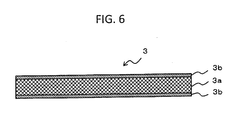
- FIG. 6 is a schematic cross-sectional view for illustrating the constitutions of the collectors in the conventional technologies.
- a conductive material layer 3b is homogeneously formed on the surface of a substrate 3a composed of a metal foil. Namely, the whole surface of the substrate 3a is covered with the conductive material layer 3b.
- the conductive material layer 3b when the conductive material layer 3b is homogeneously formed on the surface of the substrate 3a, there is a problem that the conductive material layer 3b hinders welding to worsen weldability when a metal-made tab (not shown in the figure) or the like for electrically connecting the collector 3 and a terminal of a battery, for preparing the battery using the collector 3, is welded on the surface.
- an electrode material which is constituted so that a conductive material is disposed in an island shape on the surface of a substrate.
- island structure As required, it has been desired to further improve adhesion between the conductive material disposed in the island shape (hereinafter referred to as island structure as required) on the substrate surface and the substrate.
- an active material layer is further applied and pressed on the island structure of the conductive material, so that the adhesion between the active material layer and the substrate is secured.
- the island structure of the conductive material tends to be easily peeled by handling of the collector and contact of the surface of the collector with a roller equipped on a coating machine for the active material layer after the step of the formation of the island structure of the conductive material and throughout the coating step of the active material layer. Consequently, it is considered that the effect of reducing the contact resistance is decreased by the peeling of the island structure of the conductive material.
- the present invention has been devised in view of the above-described problem and an object of the present invention is to provide: an electrode material which has excellent tab weldability, realizes reduction of the contact resistance with the active material layer, and has good adhesion between the conductive material disposed in the island shape and the substrate; a method for manufacturing the same; an electrode using the electrode material; and a secondary battery which realizes reduction of internal resistance by using the electrode.
- the electrode material according to the present invention contains: a substrate including a metal foil; and a conductive material placed on at least one surface of the substrate, wherein the conductive material is disposed in an island shape on the surface of the substrate when observed with a visual field of 300 ⁇ m square, and the conductive material is fixed to the surface of the substrate together with a hydrophobic resin and a water-soluble resin.
- the surface of the substrate including the metal foil with the conductive material such as carbon has a portion which is not covered with the conductive material.
- the portion which is not covered with the conductive material becomes 20% or more. Therefore, in the case where the electrode material is used as a collector for an electrode in a lithium ion secondary battery, it becomes easy to weld a metal-made tab for connecting the collector and a terminal of the battery.
- the conductive material is placed on the surface of the substrate so that the coverage preferably becomes 1 % or more, in the case where the electrode material is used as a collector for an electrode in a lithium ion secondary battery, the contact resistance between the collector and the active material layer laminated on the collector is reduced. Further, the adhesion between the conductive material and the substrate is improved by the hydrophobic resin, and a coatability of the substrate with a slurry containing the conductive material on the substrate is improved by the water-soluble resin in the manufacturing step. Thereby, the island structure is disposed in an island structure as a mixture of the conductive material and these resins with good adhesion to the substrate that is a metal foil.
- the attached amount of the sum of the conductive material, the water-soluble resin, and the hydrophobic resin per unit area on the surface of the substrate is preferably in the range of 0.01 to 0.50 g/m 2 .
- the conductive material may be placed on one surface of the substrate or may be placed on both surfaces of the substrate, but the range of the above attached amount shows a preferable range on each surface on which the conductive material is placed.
- the conductive material is disposed in the island shapes on the surface of the substrate by controlling the attached amount to the above range and the coverage is adjusted so that the substrate is appropriately exposed by controlling the attached amount to 0.50 g/m 2 or less, so that the metal-made tab or the like is satisfactorily welded. Moreover, by controlling the attached amount to 0.01 g/m 2 or more, in the case where the electrode material is used, for example, as a collector for the electrode in a lithium ion secondary battery, the contact resistance between the collector and the active material layer laminated on the collector is reduced.
- the method for manufacturing the electrode material according to the present invention includes an application step of applying a slurry containing the conductive material, the water-soluble resin, and an aqueous emulsion solution of the hydrophobic resin on the surface of the substrate, and a drying step of drying the slurry in this order, wherein the conductive material is agglomerated in the solution before or after the slurry is applied on the substrate.
- the hydrophobic resin is homogeneously dispersed in the slurry. Moreover, since the water-soluble resin is mixed into the slurry, in the application step, wettability of the slurry containing the water-soluble resin is improved and thus the slurry is satisfactorily applied without being repelled on the surface of the substrate to form drops. Further, since the slurry containing the conductive material to be applied on the surface of the substrate is controlled so that the conductive material is agglomerated before application or after application, the conductive material in the slurry applied on the surface of the substrate is disposed in the island shape on the surface of the substrate. By drying the slurry in the drying step, the conductive material is fixed to the surface of the substrate together with the hydrophobic resin and the water-soluble resin.
- the slurry containing carbon as the conductive material in an amount of 0.1 to 7% by mass is applied on the surface of the substrate.
- the conductive material is appropriately agglomerated in the slurry before or after the application on the substrate and the conductive material is disposed in the island shape on the surface of the substrate.
- the slurry contains the water-soluble resin in an amount of 0.25% by mass or more and the hydrophobic resin in an amount of 0.01% by mass or more, and a sum of the amount of the water-soluble resin and the amount of the hydrophobic resin in the slurry is 11% by mass or less.
- the wettability of the slurry with respect to the substrate is appropriately improved by the water-soluble resin having the content in this range and the slurry is satisfactorily applied on the substrate.
- the island structure is fixed to the substrate with good adhesion by the hydrophobic resin having the content in this range.
- the effect of reducing the contact resistance can be obtained by controlling the content of all the resins to 11% by mass or less.
- the electrode in a secondary battery according to the present invention is an electrode in a secondary battery using the above-described electrode material, wherein an active material layer is formed on a surface of the conductive material in the electrode material.
- the contact resistance between the electrode material that is a collector and the active material layer is reduced by the conductive material disposed in the island shape on the surface of the substrate.
- the secondary battery according to the present invention includes a positive electrode and a negative electrode, wherein at least one of the positive electrode and the negative electrode is the electrode according to the present invention.
- a conductive material is disposed in the island shape on the surface of a metal foil that is a substrate and the attached amount of the conductive material is limited, and thus, the contact resistance between the active material layer and the electrode material can be reduced while weldability of a tab or the like is secured.
- the island structure is adhered to the metal foil that is a substrate using the hydrophobic resin and water-soluble resin as binders and thus peeling of the formed island structure can be suppressed during the handling of the electrode material and in the manufacturing step before coating with the active material layer, and the effect of reducing the contact resistance by the island structure is not impaired.
- the island structure of the conductive material can be formed on the surface of the substrate with good adhesion, an electrode material having a good weldability of a tab or the like and capable of reducing the contact resistance with the active material layer, can be manufactured with stable quality. Moreover, owing to the use of an aqueous solution, an environmental load induced by solvent vapor in the manufacturing step can be reduced.
- the carbon is used in an appropriate concentration as a conductive material, an electrode material in which a suitable island structure is formed can be manufactured.
- the resins are used in appropriate concentration, an electrode material having good quality can be manufactured.
- the contact resistance between the electrode material and the active material layer can be reduced.
- the collector (electrode material) 1 is composed of a substrate 1a composed of a metal foil and a conductive material 1b disposed in the island shape on the surface of the substrate 1a. Moreover, the conductive material 1b is disposed on both surfaces of the substrate 1a. The conductive material 1b may be disposed on one surface of the substrate 1a.
- the "island shape” means a state where the conductive material 1b is disposed so that at least a part of the surface of the substrate 1a is exposed without being covered with the conductive material 1a.
- a plurality of agglomerates of the conductive material 1b may be disposed with being isolated one another as shown in FIG. 1 or the agglomerates may be joined one another to be disposed in a reticulate form.
- the collector 1 according to the present embodiment can be suitably used, for example, as a collector for an electrode in a lithium ion secondary battery.
- the electrode using the collector 1 will be described later.
- the collector 1 By controlling the collector 1 so as to have a structure in which the conductive material 1b is disposed in the island shape on the surface of the substrate 1a when observed with a visual field of 300 ⁇ m square (i.e., a square visual field having an area of about 0.1 mm 2 ) in an arbitrary region of the surface of the substrate 1a on which the conductive material 1b is disposed, in the case where the collector 1 is used as an electrode in the battery, tab weldability can be improved during welding a metal-made tab (not shown in the figure) that electrically connects the collector 1 with a terminal of the battery.
- a visual field of 300 ⁇ m square i.e., a square visual field having an area of about 0.1 mm 2
- the coverage of the surface of the substrate 1a with the conductive material 1b in the substrate 1a is preferably from 1 to 80% when observed with a visual field of 300 ⁇ m square in an arbitrary region of the surface of the substrate 1a on which the conductive material Ibis disposed.
- the coverage with the conductive material 1b is 1% or more, the contact resistance between the collector 1 and the active material layer 2 (see FIG. 2 ) to be laminated on the surface of the collector 1 in the case of using as an electrode in the secondary battery, can be further reduced.
- the above coverage is more preferably from 10 to 70%, and further preferably from 30 to 60%.
- the conductive material 1b is preferably disposed uniformly on the surface of the substrate 1a per at least a unit of the observed area. Since the conductive material 1b is disposed so as to be in the island shape within the region having a sufficiently small area, practically uniform contact resistance and tab weldability are obtained.
- the coverage of the surface of the substrate 1a with the conductive material 1b can be determined by photographing the surface of a prepared sample using SEM (scanning electron microscope) and calculating a covered area of the substrate surface with carbon included in the photographed visual field by image processing.
- the attached amount of the conductive material 1b per unit area on the surface of the substrate 1a is preferably in the range of 0.01 to 0.50 g/m 2 as the attached amount of the sum of the conductive material 1b and the water-soluble resin and hydrophobic resin that are binders and are not shown in the figure.
- the attached amount is more preferably 0.03 g/m 2 or more, and further preferably 0.05 g/m 2 or more.
- the attached amount is more preferably 0.40 g/m 2 or less, and further preferably 0.30 g/m 2 or less. In the case where the conductive material 1b is placed on both surfaces of the substrate 1a, it is preferred to control the attached amount to the range on each surface.
- the conductive material 1b is disposed in the island shape on the surface of the substrate 1a.
- the attached amount to preferably 0.50 g/m 2 or less, more preferably 0.40 g/m 2 or less, and further preferably 0.30 g/m 2 or less, the coverage becomes such one that the surface of the substrate 1a is appropriately exposed, so that good tab weldability is obtained.
- the attached amount to preferably 0.01 g/m 2 or more, more preferably 0.03 g/m 2 or more, and further preferably 0.05 g/m 2 or more, the contact resistance between the collector 1 and the active material layer 2 (see FIG. 2 ) to be laminated on the surface of the collector 1 in the case of using as an electrode in the secondary battery, can be further reduced.
- the attached amount of the conductive material 1b per unit area on the surface of the substrate 1a can be determined as follows. First, the mass of a sample obtained by applying a solution containing the conductive material 1b, the water-soluble resin, and the hydrophobic resin on the substrate 1 a and drying the solution, is measured. Then, the sample surface is wiped with water and alcohol and the mass thereof after removal of the conductive material 1b, the water-soluble resin, and the hydrophobic resin, is measured. By dividing mass difference between them by the area of the sample, the attached amount of the conductive material 1b per unit area on the surface of the substrate 1a can be calculated.
- the substrate 1a a metal such as aluminum (Al) or copper (Cu) that is commonly used as an electrode material for secondary batteries, can be used.
- the substrate 1 a is generally used in a form of a foil having a thickness of about 5 to 50 ⁇ m.
- rolling may be performed to achieve thinning after the solution containing the conductive material 1b is applied on the plate-shaped or thick foil-shaped substrate 1a and dried.
- the substrate 1a is not limited to Al, Cu and the like having a specific composition and, in the case of using as an electrode, various pure metals and alloys thereof suitable for the use environment of the electrode can be used.
- the conductive material 1b is disposed in the island shape so that it covers 1 to 80% of the surface of the substrate 1a when observed with a visual field of 300 ⁇ m square and reduces the contact resistance between the collector 1, which is constituted of the conductive material together with the substrate 1a, and the active material layer (see FIG. 2 ).
- a carbonaceous conductive material (carbon) can be used as the conductive material 1b.
- carbonaceous conductive material natural or artificial crystalline graphite, expanded graphite, artificial graphite, pyrolytic graphite, or various carbon blacks such as acetylene black, can be used.
- the binder (not shown in the figure) is constituted by a hydrophobic resin for improving adhesion between the island structure composed of the conductive material 1b and the surface of the substrate 1a and a water-soluble resin for improving applicability when a solution containing the hydrophobic resin and the conductive material 1b is applied on the surface of the substrate 1a.
- a hydrophobic resin for improving adhesion between the island structure composed of the conductive material 1b and the surface of the substrate 1a
- a water-soluble resin for improving applicability when a solution containing the hydrophobic resin and the conductive material 1b is applied on the surface of the substrate 1a.
- the hydrophobic resin is necessarily mixed with the water-soluble resin
- the hydrophobic resin is preferably a resin capable of forming an aqueous emulsion.
- a hydrophobic resin for example, one kind or two or more kinds as a mixture selecting from polyethylene-based resins, polypropylene resins, polyester resins, urethane-based resins, acrylic resins and the like, can be used.
- water-soluble resin for example, one kind or two or more kinds as a mixture selecting from carboxyvinyl polymers, carboxymethyl cellulose and salts thereof (sodium salt, ammonium salt), polyvinyl alcohol and the like, can be used.
- An electrode 10 shown in FIG. 2 is constituted by the collector 1 according to the present embodiment and the active material layer 2 laminated on the surfaces (both surfaces) of the collector 1.
- a metal such as Al or an Al alloy can be used as the substrate of the collector 1.
- conventional materials for example, lithium-containing oxides such as LiCoO 2 , LiNiO 2 , and LiMn 2 O 4 can be used.
- a method for manufacturing the active material layer 2 in the positive electrode is also not particularly limited and the layer can be manufactured by conventional methods, for example, by adding a binder, and if needed, a conductive material, a solvent and the like, to the powdery lithium-containing oxide described above and thoroughly kneading them, and subsequently applying the kneaded article on the collector 1, followed by drying and pressing.
- the active material layer 2 may be laminated on one surface on which the conductive material 1b has been placed.
- the substrate of the collector 1 a metal such as Cu, a Cu alloy, nickel (Ni), an Ni alloy or stainless steel, can be used.
- a negative electrode active material for example, a graphite-based carbon material can be used, and production can be made in a similar manner as in the method for manufacturing the active material layer 2 in the positive electrode.
- the lithium ion secondary battery (secondary battery) 20 shown in FIG. 3 includes a positive electrode 11 and a negative electrode 12 that are the electrode 10 using the collector 1 according to the present embodiment, a separator 13, and an electrolytic solution 14.
- the positive electrode 11 and the negative electrode 12 are separated by the separator 13, and the electrolytic solution 14 fills the space between the positive electrode 11 and the negative electrode 12 and the separator 13.
- the entire lithium ion secondary battery 20 is housed in a vessel (not shown in the figure), and a metal-made tab (not shown in the figure) is welded to each of the positive electrode 11 and the negative electrode 12, which are electrically connected to an electrode terminal (not shown in the figure).
- respective active material layers 2 containing each of the above-described positive electrode active material and negative electrode active material are formed on the surface of the collector 1 according to the present embodiment.
- the separator 13 and the electrolytic solution 14 can be each constituted using conventional materials.
- a polyethylene-based microporous film having a thickness of 20 to 30 ⁇ m can be used.
- the electrolytic solution 14 for example, a non-aqueous electrolytic solution obtained by dissolving an electrolyte such as LiPF 6 or LiBF 4 in an organic solvent such as propylene carbonate or ethylene carbonate, can be used.
- the method for manufacturing the collector 1 in the present embodiment includes an application step S1 and a drying step S2 in this order.
- the collector 1 can be prepared by a manufacturing method including the application step S1 of applying a slurry containing the conductive material 1b, an aqueous emulsion of the hydrophobic resin and the water-soluble resin on the surface of the substrate 1a composed of a metal foil and agglomerating the conductive material 1b in the slurry before or after the application on the substrate 1a, and the drying step S2 of drying the slurry.
- the conductive material 1b homogeneously dispersed immediately after the slurry is formulated is agglomerated with the passage of time.
- the conductive material 1b is agglomerated before or after the application of the formulated slurry on the surface of the substrate 1a.
- the conductive material 1b form a state of being agglomerated in the island shape.
- the slurry is dried to fix the conductive material 1b in the island shape on the surface of the substrate 1a.
- the hydrophobic resin fills the space between the substrate 1a, and the particles of the conductive material 1b being in contact with the substrate 1a and the island structure of the conductive material 1b can be strongly fixed to the surface of the substrate 1a with good adhesion.
- the island structure is fixed to the surface of the substrate 1a as a mixed body of the conductive material 1b, the hydrophobic resin, and the water-soluble resin to be described later.
- the conductive material 1b In order to agglomerate the conductive material 1b so as to be an ideal island structure, it is effective to control the particle diameter and concentration of the conductive material 1b and the concentration of the hydrophobic resin and the water-soluble resin as binders, which are contained in the slurry. In the case where the particle diameter and concentration of the conductive material 1b and the concentration of the binders are controlled, viscosity of the slurry is varied, so that coatability and distribution of the conductive material 1b after drying are changed. In the case of using carbon as the conductive material 1b, it is preferred to use carbon having an average particle diameter of 0.01 to 1 ⁇ m. Also, the state where carbon is contained in an amount of 0.1 to 7% by mass in the slurry is preferred.
- the average particle diameter of the carbon as the conductive material 1b By controlling the average particle diameter of the carbon as the conductive material 1b to 1 ⁇ m or less and the concentration of the carbon to 0.1 % by mass or more, the island structure is formed and also contact points between the carbon as the conductive material 1b and the metal foil as the substrate 1a sufficiently exist, so that the effect of reducing the contact resistance between the collector 1 and the active material layer 2 (see FIG. 2 ) can be obtained.
- the island structure of the conductive material 1b can be disposed on the substrate 1a that is a metal foil with good adhesion. Therefore, when the electrode is prepared, peeling of the island structure of the conductive material 1b can be prevented until the application step of the active material layer 2 (see FIG. 2 ).
- the concentration of the hydrophobic resin is preferably 0.01% by mass or more and about 11% by mass or less, more preferably 0.10% by mass or more, and further preferably 0.25% by mass or more.
- the hydrophobic resin and the water-soluble resin can be mixed.
- hydrophobic resin for example, one kind or two or more kinds as a mixture selecting from polyethylene-based resins, polypropylene resins, polyester resins, urethane-based resins, acrylic resins and the like, can be used.
- the slurry that is an aqueous emulsion solution of the hydrophobic resin in which the conductive material 1b is dispersed is repelled in the above-described concentration range of the hydrophobic resin owing to water repellency of the surface of the substrate 1a, and hence there is such a problem in coatability that the slurry becomes in a so-called water-repelled state to form drops.
- the concentration of the hydrophobic resin is too high, the contact resistance (i.e., internal resistance of the secondary battery) becomes high, so that characteristics on the contact resistance cannot be satisfied.
- wettability with respect to the substrate 1a that is a metal foil is improved by mixing the water-soluble resin into an aqueous emulsion solution of the hydrophobic resin.
- coating of the substrate 1a with the coating solution becomes possible without forming drops, and the island structure of the conductive material 1b can be fixed to the substrate 1a with good adhesion.
- water-soluble resin for example, one kind or two or more kinds as a mixture selecting from carboxyvinyl polymers, carboxymethyl cellulose and salts thereof (sodium salt, ammonium salt), polyvinyl alcohol and the like, can be used.
- the concentration of the water-soluble resin is preferably controlled to 0.25% by mass or more and about 11% by mass or less.
- total resin concentration of the hydrophobic resin and the water-soluble resin is preferably controlled to 0.5 to 11% by mass.
- Good coatability and adhesion can be obtained by controlling the amount to 0.5% by mass or more and a good effect of reducing the contact resistance (internal resistance of the secondary battery) can be obtained by controlling the amount to 11% by mass or less.
- a carbonaceous material can be used as the conductive material 1b.
- natural or artificial crystalline graphite, expanded graphite, artificial graphite, pyrolytic graphite, and various carbon blacks such as acetylene black can be used as the conductive material 1b.
- the solution containing the conductive material 1b on the surface of the substrate 1a application methods by means of various coaters such as a bar coater, a roll coater, a gravure coater, a reverse gravure coater, a dip coater, and a spray coater, can be used.
- the conductive material 1b is applied on both surfaces or one surface of the substrate 1a.
- the drying step S2 is a step of vaporizing the solvent after the application step S1.
- drying may be performed at room temperature or drying under heating may be performed by using a heat treatment furnace or the like according to needs.
- drying temperature is preferably controlled to 100°C to 170°C, and more preferably 140°C to 170°C as a temperature at which water as a solvent of the aqueous emulsion solution is easily evaporated (reason for lower limit) and strength of the metal foil as the substrate 1a is not lowered (reason for upper limit).
- the temperature is controlled to 140°C or higher, the hydrophobic resin is softened by heat and thus the adhesion between the substrate 1a and the hydrophobic resin is improved. As a result, the adhesion between the substrate 1a and the conductive material 1b can be further improved.
- drying time is not particularly limited but, in the case where drying is conducted at 100°C to 170°C, the time is preferably controlled to 0.1 minutes to 5 minutes.
- the solvent can be sufficiently evaporated by controlling the time to 0.1 minutes or more and a decrease in strength of the metal foil as the substrate 1a can be prevented by controlling the time to 5 minutes or less.
- Samples were prepared by the following methods.
- hydrophobic resin As a hydrophobic resin, an aqueous emulsion solution using polypropylene (PP) or polyethylene (PE) was prepared and the prepared aqueous emulsion solution was diluted with pure water to use. For comparison, a sample using no hydrophobic resin was also prepared.
- PP polypropylene
- PE polyethylene
- CMC carboxymethyl cellulose sodium salt
- a sample using no water-soluble resin was also prepared.
- carbon black As a conductive material, carbon black (TOKABLACK #4300 manufactured by Tokai Carbon Co., Ltd.) having an average particle diameter of 0.06 ⁇ m was used.
- the above slurry containing the carbon black was applied on both surfaces of the substrate and, for the samples for evaluation of other items, the slurry was applied on one surface of the substrate.
- drying was performed by keeping in an oven at 150°C for 1 minute.
- a roller (having a diameter of 90 mm, a width of 50 mm and mass of 700 g) to which a pressure-sensitive adhesive tape having a pressure-sensitive adhesive force of 2 N/40 mm, a width of 40 mm, a length of 120 mm, and a thickness of 0.08 mm had been attached was rolled on the surface of a sample by 100 mm and area of peeled carbon black was estimated.
- the case where no peeling of carbon black was observed was ranked as excellent (O)
- the case where 20% or less of peeling was observed was ranked as good ( ⁇ )
- the case where farther peeling was observed was ranked as bad (x).
- the coverage with the conductive material (carbon) was determined by photographing the surface of a sample at a magnification of 300 using a field emission-type scanning electron microscope (FE-SEM) SU-70 manufactured by Hitachi Ltd. and calculating an area of the substrate surface covered with carbon included in the photographed visual field by image processing.
- FE-SEM field emission-type scanning electron microscope
- Both surfaces of a sample on which the carbon black (conductive material) had been formed was coated at a thickness of 25 ⁇ m per one surface with a slurry obtained by mixing lithium cobaltate, acetylene black and PVdF (polyvinylidene fluoride) to prepare a positive electrode.
- a slurry obtained by mixing lithium cobaltate, acetylene black and PVdF (polyvinylidene fluoride) to prepare a positive electrode.
- a negative electrode one obtained by coating both surfaces of the Al foil with graphite at a thickness of 35 ⁇ m per one surface was used.
- a battery cell was prepared using an HS flat cell manufactured by Hohsen Corp.
- a discharge test was carried out at plural current values of 0.2 C to 10 C.
- a relationship between the current value and voltage value at discharging a capacity of 1 mAh was plotted, and internal resistance was calculated based on the slope of the straight line obtained by the plotting.
- a positive electrode was prepared in the same manner as in the case of the other samples, and a battery cell was similarly prepared using the positive electrode.
- a discharge curve was determined similarly to the battery cells using the other samples, and internal resistance was calculated. Then, it was judged that those exhibiting reduced internal resistance in comparison to the internal resistance of the battery cell prepared using the collector composed of only the substrate had an effect of reducing the internal resistance.
- the internal resistance of the battery cell prepared using only the Al foil that is a substrate as the collector was 45 ⁇ .
- the contact resistance (effect of reducing resistance) in the case of using the Cu foil as a substrate was measured as follows.
- Both surfaces of a sample was sandwiched with two sheets of a carbon cloth, the outsides were further sandwiched with two sheet of a copper electrode having a contact area of 1 cm 2 , and pressurization was conducted by imparting a load of 1 kgf (9.8 N) to the copper electrode. Then, a current of 7.4 mA was applied using a direct current power source and a voltage imparted between the carbon cloths was measured with a voltmeter. The contact resistance was determined by calculation from the above current value, contact area, and measured voltage. Similar measurement was performed using the substrate alone and it was judged that those exhibiting reduced contact resistance in comparison to the case of only the substrate had an effect of reducing the contact resistance. The contact resistance in the case of only the Cu foil as a substrate, which was not subjected to any surface treatment, was about 100 [m ⁇ cm 2 (milliohm square centimeter)].
- the attached amount of the conductive material per unit area on the substrate was measured by the following procedure.
- the attached amount of the conductive material per unit area on the substrate is an attached amount per unit area on one surface of the substrate and is an attached amount of the sum of the carbon black as a conductive material and the water-soluble resin and hydrophobic resin as binders.
- the mass of a sample obtained by applying a solution containing the conductive material, the water-soluble resin and the hydrophobic resin on the substrate and drying it was measured. Then, the surface of the sample was wiped with water and dried. Subsequently, the same surface of the sample was wiped with alcohol to remove the hydrophilic resin, the lipophilic resin, and the conductive material attached on the foil. The mass of the sample after the removal of the resins and the conductive material was measured. The attached amount of the conductive material per unit area on the substrate was calculated by dividing the mass difference of the sample before the removal of the conductive material and after the removal of the conductive material by the area of the substrate.
- an Al foil or Cu foil having a size of 50 mm square i.e., area of 2,500 mm 2
- the substrate i.e., sample
- Tables 1 and 2 show a list of characteristic evaluation results and judgment results of samples prepared using the Al foil as a substrate.
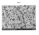
- Samples No. 1 to No. 7 were satisfactory in all evaluations (coatability, adhesion, internal resistance, weldability, and coverage) and it was confirmed that carbon black (conductive material) was disposed in the island shape by the observation using SEM.
- the SEM (scanning electron microscope) picture shown in FIG. 5 is one obtained by photographing the surface of Sample No. 1 and, in FIG. 5 , one division shown in the lower right part is 10 ⁇ m.
- Sample No.8 is a comparative example, which is a case where a battery cell is prepared using an electrode in which a collector of only the Al foil as a substrate is used without using carbon black (conductive material).
- the internal resistance of the battery cell was 45 ⁇ .
- Sample No. 9 is the case where the concentration of carbon black (conductive material) in the slurry is so high as 14% by mass. Therefore, the coverage with carbon black is so high as 100% and no island structure was present, so that weldability was not excellent.
- Sample No. 10 is a result of the case where only the water-soluble resin was used without using the hydrophobic resin.
- the coverage was 36%, which fallen within the range of 1 to 80%, and the coatability, the effect of reducing the internal resistance, and the weldability were satisfactory. However, sufficient adhesion was not obtained since the hydrophobic resin was not used.
- Sample No. 11 is a result of the case where only the hydrophobic resin was used without using the water-soluble resin. Since the water-soluble resin was not used, it was impossible to apply the slurry containing carbon black on the surface of the substrate satisfactorily.
- Sample No. 23 is the case where the concentration of carbon black (conductive material) in the slurry is so high as 10% by mass. Therefore, the attached amount of the conductive material on the substrate surface was large and thus no island structure was formed, so that the weldability (1) was not excellent.
- Table 3 shows a list of characteristic evaluation results and judgment results of samples prepared using the Cu foil as a substrate.
- " ⁇ ” represents a good judgment result and "x” represents a bad judgment result.
- Table 3 a numerical value judged as bad was underlined.
- Sample No. 29 is a comparative example, which is the case where a battery cell was prepared using an electrode in which a collector of only the Cu foil as a substrate was used without using carbon black (conductive material).
- the contact resistance was 108 m ⁇ cm 2 .
- Sample No. 30 is the case where the concentration of carbon black (conductive material) in the slurry is so high as 10% by mass. Therefore, the coverage with carbon black was so high as 100% and no island structure was present, so that the weldability (2) was not excellent.
- Sample No. 31 is a result of the case where only the hydrophobic resin was used without using the water-soluble resin. Since the water-soluble resin was not used, it was impossible to apply the slurry containing carbon black on the surface of the substrate satisfactorily.
- Sample No. 32 is a result of the case where only the hydrophilic resin was used without using the hydrophobic resin.
- the coverage was 45%, which fallen within the range of 1 to 80%, and the coatability, the effect of reducing the internal resistance, and the weldability (2) were satisfactory. However, sufficient adhesion was not obtained since the hydrophobic resin was not used.
- a conductive material is disposed in the island shape on the surface of a metal foil that is a substrate and the attached amount of the conductive material is limited, and thus, the contact resistance between the active material layer and the electrode material can be reduced while weldability of a tab or the like is secured.
- the island structure is adhered to the metal foil that is a substrate using the hydrophobic resin and water-soluble resin as binders and thus peeling of the formed island structure can be suppressed during the handling of the electrode material and in the manufacturing step before coating with the active material layer, and the effect of reducing the contact resistance by the island structure is not impaired.
- the island structure of the conductive material can be formed on the surface of the substrate with good adhesion, an electrode material having a good weldability of a tab or the like and capable of reducing the contact resistance with the active material layer, can be manufactured with stable quality. Moreover, owing to the use of an aqueous solution, an environmental laod induced by solvent vapor in the manufacturing step can be reduced.
- the carbon is used in an appropriate concentration as a conductive material, an electrode material in which a suitable island structure is formed can be manufactured.
- the resins are used in appropriate concentration, an electrode material having good quality can be manufactured.
- the contact resistance between the electrode material and the active material layer can be reduced.
Landscapes
- Chemical & Material Sciences (AREA)
- Engineering & Computer Science (AREA)
- Materials Engineering (AREA)
- Chemical Kinetics & Catalysis (AREA)
- Electrochemistry (AREA)
- General Chemical & Material Sciences (AREA)
- Composite Materials (AREA)
- Cell Electrode Carriers And Collectors (AREA)
- Battery Electrode And Active Subsutance (AREA)
Abstract
Description
- The present invention relates to an electrode material to be used for an electrode in a secondary battery, a method for manufacturing the same, an electrode using the electrode material, and a secondary battery using the electrode.
- Studies on collectors in which a carbonaceous conductive material is applied on a metal foil such as an aluminum foil or a copper foil to be used as a substrate of an electrode for a secondary battery have been hitherto conducted in various research institutes. Also, a large number of patent applications have been filed and, for example,
Patent Documents 1 to 4 are exemplified. -
Patent Documents Patent Document 3 describes a collector in which a conductive layer composed of a carbon powder (conductive material) and a binder is placed between active materials. Further, Patent Document 4 describes a collector in which a conductive coating layer containing carbon as a conductive agent (conductive material) is placed on the surface. In these, internal resistance of batteries using these collectors is reduced by reducing contact resistance between the collectors and active material layers formed thereon, and thus it has been intended to improve high-speed charge-discharge characteristics and cycle characteristics of the batteries. -
- Patent Document 1:
JP-A-2007-226969 - Patent Document 2:
JP-A-2010-135338 - Patent Document 3:
JP-A-9-97625 - Patent Document 4:
JP-A-2001-351612 - Here, the constitutions of the collectors in conventional technologies described in
Patent Documents 1 to 4 are collectively explained with reference toFIG. 6. FIG. 6 is a schematic cross-sectional view for illustrating the constitutions of the collectors in the conventional technologies. As shown inFIG. 6 , in acollector 3 in the conventional technologies, aconductive material layer 3b is homogeneously formed on the surface of asubstrate 3a composed of a metal foil. Namely, the whole surface of thesubstrate 3a is covered with theconductive material layer 3b. - As shown in
FIG. 6 , when theconductive material layer 3b is homogeneously formed on the surface of thesubstrate 3a, there is a problem that theconductive material layer 3b hinders welding to worsen weldability when a metal-made tab (not shown in the figure) or the like for electrically connecting thecollector 3 and a terminal of a battery, for preparing the battery using thecollector 3, is welded on the surface. - In order to solve such a problem, the applicant of the present application has invented an electrode material (collector) which is constituted so that a conductive material is disposed in an island shape on the surface of a substrate. Thereby, reduction of contact resistance and weldability can be both achieved.
- Here, for the following reason, it has been desired to further improve adhesion between the conductive material disposed in the island shape (hereinafter referred to as island structure as required) on the substrate surface and the substrate. In the case of preparing an electrode using the collector in which the conductive material is disposed in an island shape on the substrate surface, an active material layer is further applied and pressed on the island structure of the conductive material, so that the adhesion between the active material layer and the substrate is secured. However, in the case where the adhesion between the island structure of the conductive material and the substrate is weak, the island structure of the conductive material tends to be easily peeled by handling of the collector and contact of the surface of the collector with a roller equipped on a coating machine for the active material layer after the step of the formation of the island structure of the conductive material and throughout the coating step of the active material layer. Consequently, it is considered that the effect of reducing the contact resistance is decreased by the peeling of the island structure of the conductive material.
- The present invention has been devised in view of the above-described problem and an object of the present invention is to provide: an electrode material which has excellent tab weldability, realizes reduction of the contact resistance with the active material layer, and has good adhesion between the conductive material disposed in the island shape and the substrate; a method for manufacturing the same; an electrode using the electrode material; and a secondary battery which realizes reduction of internal resistance by using the electrode.
- In order to solve the above problems, the electrode material according to the present invention contains: a substrate including a metal foil; and a conductive material placed on at least one surface of the substrate, wherein the conductive material is disposed in an island shape on the surface of the substrate when observed with a visual field of 300 µm square, and the conductive material is fixed to the surface of the substrate together with a hydrophobic resin and a water-soluble resin.
- According to such a constitution, the surface of the substrate including the metal foil with the conductive material such as carbon has a portion which is not covered with the conductive material. Preferably, by controlling the coverage with the conductive material to 80% or less, the portion which is not covered with the conductive material becomes 20% or more. Therefore, in the case where the electrode material is used as a collector for an electrode in a lithium ion secondary battery, it becomes easy to weld a metal-made tab for connecting the collector and a terminal of the battery. Moreover, by placing the conductive material on the surface of the substrate so that the coverage preferably becomes 1 % or more, in the case where the electrode material is used as a collector for an electrode in a lithium ion secondary battery, the contact resistance between the collector and the active material layer laminated on the collector is reduced. Further, the adhesion between the conductive material and the substrate is improved by the hydrophobic resin, and a coatability of the substrate with a slurry containing the conductive material on the substrate is improved by the water-soluble resin in the manufacturing step. Thereby, the island structure is disposed in an island structure as a mixture of the conductive material and these resins with good adhesion to the substrate that is a metal foil.
- Furthermore, in the electrode material according to the present invention, the attached amount of the sum of the conductive material, the water-soluble resin, and the hydrophobic resin per unit area on the surface of the substrate is preferably in the range of 0.01 to 0.50 g/m2. Here, the conductive material may be placed on one surface of the substrate or may be placed on both surfaces of the substrate, but the range of the above attached amount shows a preferable range on each surface on which the conductive material is placed.
- According to such a constitution, the conductive material is disposed in the island shapes on the surface of the substrate by controlling the attached amount to the above range and the coverage is adjusted so that the substrate is appropriately exposed by controlling the attached amount to 0.50 g/m2 or less, so that the metal-made tab or the like is satisfactorily welded. Moreover, by controlling the attached amount to 0.01 g/m2 or more, in the case where the electrode material is used, for example, as a collector for the electrode in a lithium ion secondary battery, the contact resistance between the collector and the active material layer laminated on the collector is reduced.
- The method for manufacturing the electrode material according to the present invention includes an application step of applying a slurry containing the conductive material, the water-soluble resin, and an aqueous emulsion solution of the hydrophobic resin on the surface of the substrate, and a drying step of drying the slurry in this order, wherein the conductive material is agglomerated in the solution before or after the slurry is applied on the substrate.
- According to such a method, since an aqueous emulsion solution of the hydrophobic resin is used, the hydrophobic resin is homogeneously dispersed in the slurry. Moreover, since the water-soluble resin is mixed into the slurry, in the application step, wettability of the slurry containing the water-soluble resin is improved and thus the slurry is satisfactorily applied without being repelled on the surface of the substrate to form drops. Further, since the slurry containing the conductive material to be applied on the surface of the substrate is controlled so that the conductive material is agglomerated before application or after application, the conductive material in the slurry applied on the surface of the substrate is disposed in the island shape on the surface of the substrate. By drying the slurry in the drying step, the conductive material is fixed to the surface of the substrate together with the hydrophobic resin and the water-soluble resin.
- In the method for manufacturing the electrode material according to the present invention, it is preferred that, in the application step, the slurry containing carbon as the conductive material in an amount of 0.1 to 7% by mass is applied on the surface of the substrate.
- According to such a method, the conductive material is appropriately agglomerated in the slurry before or after the application on the substrate and the conductive material is disposed in the island shape on the surface of the substrate.
- In the method for manufacturing the electrode material according to the present invention, it is preferred that, in the application step, the slurry contains the water-soluble resin in an amount of 0.25% by mass or more and the hydrophobic resin in an amount of 0.01% by mass or more, and a sum of the amount of the water-soluble resin and the amount of the hydrophobic resin in the slurry is 11% by mass or less.
- According to such a method, the wettability of the slurry with respect to the substrate is appropriately improved by the water-soluble resin having the content in this range and the slurry is satisfactorily applied on the substrate. Moreover, the island structure is fixed to the substrate with good adhesion by the hydrophobic resin having the content in this range. Further, the effect of reducing the contact resistance can be obtained by controlling the content of all the resins to 11% by mass or less.
- The electrode in a secondary battery according to the present invention is an electrode in a secondary battery using the above-described electrode material, wherein an active material layer is formed on a surface of the conductive material in the electrode material.
- According to such a constitution, the contact resistance between the electrode material that is a collector and the active material layer is reduced by the conductive material disposed in the island shape on the surface of the substrate.
- The secondary battery according to the present invention includes a positive electrode and a negative electrode, wherein at least one of the positive electrode and the negative electrode is the electrode according to the present invention.
- According to such a constitution, since the contact resistance between the electrode material that is a collector and the active material layer is reduced in the electrode in the secondary battery, the internal resistance is reduced in the secondary battery.
- According to the electrode material of the present invention, a conductive material is disposed in the island shape on the surface of a metal foil that is a substrate and the attached amount of the conductive material is limited, and thus, the contact resistance between the active material layer and the electrode material can be reduced while weldability of a tab or the like is secured. Moreover, the island structure is adhered to the metal foil that is a substrate using the hydrophobic resin and water-soluble resin as binders and thus peeling of the formed island structure can be suppressed during the handling of the electrode material and in the manufacturing step before coating with the active material layer, and the effect of reducing the contact resistance by the island structure is not impaired.
- According to the method for manufacturing the electrode material of the present invention, since the island structure of the conductive material can be formed on the surface of the substrate with good adhesion, an electrode material having a good weldability of a tab or the like and capable of reducing the contact resistance with the active material layer, can be manufactured with stable quality. Moreover, owing to the use of an aqueous solution, an environmental load induced by solvent vapor in the manufacturing step can be reduced.
- Further, according to the method for manufacturing the electrode material of the present invention, since the carbon is used in an appropriate concentration as a conductive material, an electrode material in which a suitable island structure is formed can be manufactured.
- Furthermore, according to the method for manufacturing the electrode material of the present invention, since the resins are used in appropriate concentration, an electrode material having good quality can be manufactured.
- According to the electrode of the present invention, the contact resistance between the electrode material and the active material layer can be reduced.
- Moreover, according to the secondary battery of the present invention, internal resistance can be reduced.
-
-
FIG. 1 is a schematic cross-sectional view for illustrating the structure of the collector according to the present invention. -
FIG. 2 is a schematic cross-sectional view for illustrating the structure of an electrode using the collector according to the present invention. -
FIG. 3 is a schematic cross-sectional view for illustrating the structure of a secondary battery using the electrode according to the present invention. -
FIG. 4 is a flow chart showing a flow of the method for manufacturing a collector according to the present invention. -
FIG. 5 is a picture of the surface of a sample of the collector according to Example on a scanning electron microscope. -
FIG. 6 is a schematic cross-sectional view for illustrating the structure of collectors according to conventional technologies. - The following will describe an embodiment of the electrode material (hereinafter also referred to as collector) according to the present invention in detail.
- The structure of the collector according to the present embodiment will be described with reference to
FIG. 1 . - The collector (electrode material) 1 according to the present embodiment is composed of a substrate 1a composed of a metal foil and a
conductive material 1b disposed in the island shape on the surface of the substrate 1a. Moreover, theconductive material 1b is disposed on both surfaces of the substrate 1a. Theconductive material 1b may be disposed on one surface of the substrate 1a. - In the present specification, the "island shape" means a state where the
conductive material 1b is disposed so that at least a part of the surface of the substrate 1a is exposed without being covered with the conductive material 1a. For example, a plurality of agglomerates of theconductive material 1b may be disposed with being isolated one another as shown inFIG. 1 or the agglomerates may be joined one another to be disposed in a reticulate form. - The
collector 1 according to the present embodiment can be suitably used, for example, as a collector for an electrode in a lithium ion secondary battery. The electrode using thecollector 1 will be described later. - By controlling the
collector 1 so as to have a structure in which theconductive material 1b is disposed in the island shape on the surface of the substrate 1a when observed with a visual field of 300 µm square (i.e., a square visual field having an area of about 0.1 mm2) in an arbitrary region of the surface of the substrate 1a on which theconductive material 1b is disposed, in the case where thecollector 1 is used as an electrode in the battery, tab weldability can be improved during welding a metal-made tab (not shown in the figure) that electrically connects thecollector 1 with a terminal of the battery. - Moreover, the coverage of the surface of the substrate 1a with the
conductive material 1b in the substrate 1a is preferably from 1 to 80% when observed with a visual field of 300 µm square in an arbitrary region of the surface of the substrate 1a on which the conductive material Ibis disposed. In the case where the coverage with theconductive material 1b is 1% or more, the contact resistance between thecollector 1 and the active material layer 2 (seeFIG. 2 ) to be laminated on the surface of thecollector 1 in the case of using as an electrode in the secondary battery, can be further reduced. Further, by controlling the coverage of the surface of the substrate 1a with theconductive material 1b to 80% or less, further satisfactory tab weldability can be secured. The above coverage is more preferably from 10 to 70%, and further preferably from 30 to 60%. - The
conductive material 1b is preferably disposed uniformly on the surface of the substrate 1a per at least a unit of the observed area. Since theconductive material 1b is disposed so as to be in the island shape within the region having a sufficiently small area, practically uniform contact resistance and tab weldability are obtained. - Here, the coverage of the surface of the substrate 1a with the
conductive material 1b can be determined by photographing the surface of a prepared sample using SEM (scanning electron microscope) and calculating a covered area of the substrate surface with carbon included in the photographed visual field by image processing. - Moreover, the attached amount of the
conductive material 1b per unit area on the surface of the substrate 1a is preferably in the range of 0.01 to 0.50 g/m2 as the attached amount of the sum of theconductive material 1b and the water-soluble resin and hydrophobic resin that are binders and are not shown in the figure. Also, the attached amount is more preferably 0.03 g/m2 or more, and further preferably 0.05 g/m2 or more. The attached amount is more preferably 0.40 g/m2 or less, and further preferably 0.30 g/m2 or less. In the case where theconductive material 1b is placed on both surfaces of the substrate 1a, it is preferred to control the attached amount to the range on each surface. - By controlling the attached amount to the range, the
conductive material 1b is disposed in the island shape on the surface of the substrate 1a. Moreover, by controlling the attached amount to preferably 0.50 g/m2 or less, more preferably 0.40 g/m2 or less, and further preferably 0.30 g/m2 or less, the coverage becomes such one that the surface of the substrate 1a is appropriately exposed, so that good tab weldability is obtained. Further, by controlling the attached amount to preferably 0.01 g/m2 or more, more preferably 0.03 g/m2 or more, and further preferably 0.05 g/m2 or more, the contact resistance between thecollector 1 and the active material layer 2 (seeFIG. 2 ) to be laminated on the surface of thecollector 1 in the case of using as an electrode in the secondary battery, can be further reduced. - Here, the attached amount of the
conductive material 1b per unit area on the surface of the substrate 1a can be determined as follows. First, the mass of a sample obtained by applying a solution containing theconductive material 1b, the water-soluble resin, and the hydrophobic resin on the substrate 1 a and drying the solution, is measured. Then, the sample surface is wiped with water and alcohol and the mass thereof after removal of theconductive material 1b, the water-soluble resin, and the hydrophobic resin, is measured. By dividing mass difference between them by the area of the sample, the attached amount of theconductive material 1b per unit area on the surface of the substrate 1a can be calculated. - As the substrate 1a, a metal such as aluminum (Al) or copper (Cu) that is commonly used as an electrode material for secondary batteries, can be used. In the case of using as an electrode material for secondary batteries, the substrate 1 a is generally used in a form of a foil having a thickness of about 5 to 50 µm. In the method for manufacturing the collector according to the present embodiment, in the case where a rolling step is carried out, rolling may be performed to achieve thinning after the solution containing the
conductive material 1b is applied on the plate-shaped or thick foil-shaped substrate 1a and dried. - The substrate 1a is not limited to Al, Cu and the like having a specific composition and, in the case of using as an electrode, various pure metals and alloys thereof suitable for the use environment of the electrode can be used.
- The
conductive material 1b is disposed in the island shape so that it covers 1 to 80% of the surface of the substrate 1a when observed with a visual field of 300 µm square and reduces the contact resistance between thecollector 1, which is constituted of the conductive material together with the substrate 1a, and the active material layer (seeFIG. 2 ). - As the
conductive material 1b, a carbonaceous conductive material (carbon) can be used. As the carbonaceous conductive material, natural or artificial crystalline graphite, expanded graphite, artificial graphite, pyrolytic graphite, or various carbon blacks such as acetylene black, can be used. - Moreover, with regard to the island structure composed of the
conductive material 1b, good adhesion to the surface of the substrate 1a is secured by a binder (not shown in the figure) to be mentioned later. - The binder (not shown in the figure) is constituted by a hydrophobic resin for improving adhesion between the island structure composed of the
conductive material 1b and the surface of the substrate 1a and a water-soluble resin for improving applicability when a solution containing the hydrophobic resin and theconductive material 1b is applied on the surface of the substrate 1a. Thereby, the adhesion between the substrate 1a and the island structure of theconductive material 1b is enhanced and the island structure is formed on the surface of the substrate 1a with uniform distribution. - Since the hydrophobic resin is necessarily mixed with the water-soluble resin, the hydrophobic resin is preferably a resin capable of forming an aqueous emulsion. As such a hydrophobic resin, for example, one kind or two or more kinds as a mixture selecting from polyethylene-based resins, polypropylene resins, polyester resins, urethane-based resins, acrylic resins and the like, can be used.
- Moreover, as the water-soluble resin, for example, one kind or two or more kinds as a mixture selecting from carboxyvinyl polymers, carboxymethyl cellulose and salts thereof (sodium salt, ammonium salt), polyvinyl alcohol and the like, can be used.
- Next, the constitution of the electrode in a lithium ion secondary battery using the
collector 1 according to the present embodiment is explained with reference toFIG. 2 . - An
electrode 10 shown inFIG. 2 is constituted by thecollector 1 according to the present embodiment and theactive material layer 2 laminated on the surfaces (both surfaces) of thecollector 1. In the case of constituting the positive electrode in the lithium ion secondary battery, a metal such as Al or an Al alloy can be used as the substrate of thecollector 1. Moreover, as a positive electrode active material, conventional materials, for example, lithium-containing oxides such as LiCoO2, LiNiO2, and LiMn2O4 can be used. A method for manufacturing theactive material layer 2 in the positive electrode is also not particularly limited and the layer can be manufactured by conventional methods, for example, by adding a binder, and if needed, a conductive material, a solvent and the like, to the powdery lithium-containing oxide described above and thoroughly kneading them, and subsequently applying the kneaded article on thecollector 1, followed by drying and pressing. Theactive material layer 2 may be laminated on one surface on which theconductive material 1b has been placed. - Moreover, in the case of constituting the negative electrode in the lithium ion secondary battery, as the substrate of the
collector 1, a metal such as Cu, a Cu alloy, nickel (Ni), an Ni alloy or stainless steel, can be used. Further, as a negative electrode active material, for example, a graphite-based carbon material can be used, and production can be made in a similar manner as in the method for manufacturing theactive material layer 2 in the positive electrode. - The following will describe the constitution of the lithium ion secondary battery using the
electrode 10 using thecollector 1 according to the present embodiment, with reference toFIG. 3 (seeFIG. 2 as required). - The lithium ion secondary battery (secondary battery) 20 shown in
FIG. 3 includes apositive electrode 11 and anegative electrode 12 that are theelectrode 10 using thecollector 1 according to the present embodiment, aseparator 13, and anelectrolytic solution 14. Thepositive electrode 11 and thenegative electrode 12 are separated by theseparator 13, and theelectrolytic solution 14 fills the space between thepositive electrode 11 and thenegative electrode 12 and theseparator 13. Moreover, the entire lithium ionsecondary battery 20 is housed in a vessel (not shown in the figure), and a metal-made tab (not shown in the figure) is welded to each of thepositive electrode 11 and thenegative electrode 12, which are electrically connected to an electrode terminal (not shown in the figure). - In the
positive electrode 11 and thenegative electrode 12, respectiveactive material layers 2 containing each of the above-described positive electrode active material and negative electrode active material are formed on the surface of thecollector 1 according to the present embodiment. - Moreover, the
separator 13 and theelectrolytic solution 14 can be each constituted using conventional materials. As theseparator 13, for example, a polyethylene-based microporous film having a thickness of 20 to 30 µm can be used. As theelectrolytic solution 14, for example, a non-aqueous electrolytic solution obtained by dissolving an electrolyte such as LiPF6 or LiBF4 in an organic solvent such as propylene carbonate or ethylene carbonate, can be used. - The following will describe the method for manufacturing the
collector 1 according to the present embodiment, with reference toFIG. 4 (seeFIG. 1 as required). - As shown in
FIG. 4 , the method for manufacturing thecollector 1 in the present embodiment includes an application step S1 and a drying step S2 in this order. - The
collector 1 can be prepared by a manufacturing method including the application step S1 of applying a slurry containing theconductive material 1b, an aqueous emulsion of the hydrophobic resin and the water-soluble resin on the surface of the substrate 1a composed of a metal foil and agglomerating theconductive material 1b in the slurry before or after the application on the substrate 1a, and the drying step S2 of drying the slurry. - Here, the
conductive material 1b homogeneously dispersed immediately after the slurry is formulated is agglomerated with the passage of time. Namely, theconductive material 1b is agglomerated before or after the application of the formulated slurry on the surface of the substrate 1a. In the slurry applied on the surface of the substrate 1a, theconductive material 1b form a state of being agglomerated in the island shape. Thereafter, the slurry is dried to fix theconductive material 1b in the island shape on the surface of the substrate 1a. On this occasion, the hydrophobic resin fills the space between the substrate 1a, and the particles of theconductive material 1b being in contact with the substrate 1a and the island structure of theconductive material 1b can be strongly fixed to the surface of the substrate 1a with good adhesion. Namely, the island structure is fixed to the surface of the substrate 1a as a mixed body of theconductive material 1b, the hydrophobic resin, and the water-soluble resin to be described later. - The following will describe the application step in detail.
- First, the application step S1 will be described.
- In order to agglomerate the
conductive material 1b so as to be an ideal island structure, it is effective to control the particle diameter and concentration of theconductive material 1b and the concentration of the hydrophobic resin and the water-soluble resin as binders, which are contained in the slurry. In the case where the particle diameter and concentration of theconductive material 1b and the concentration of the binders are controlled, viscosity of the slurry is varied, so that coatability and distribution of theconductive material 1b after drying are changed. In the case of using carbon as theconductive material 1b, it is preferred to use carbon having an average particle diameter of 0.01 to 1 µm. Also, the state where carbon is contained in an amount of 0.1 to 7% by mass in the slurry is preferred. By controlling the average particle diameter to 0.01 µm or more and the concentration (content) to 7% by mass or less, the viscosity of the slurry is not exceedingly increased and the agglomeration of carbon particles one another becomes not exceedingly large, and thus, the ideal island structure can be obtained. Moreover, by controlling the average particle diameter of the carbon as theconductive material 1b to 1 µm or less and the concentration of the carbon to 0.1 % by mass or more, the island structure is formed and also contact points between the carbon as theconductive material 1b and the metal foil as the substrate 1a sufficiently exist, so that the effect of reducing the contact resistance between thecollector 1 and the active material layer 2 (seeFIG. 2 ) can be obtained. - Also, by using the hydrophobic resin, the island structure of the
conductive material 1b can be disposed on the substrate 1a that is a metal foil with good adhesion. Therefore, when the electrode is prepared, peeling of the island structure of theconductive material 1b can be prevented until the application step of the active material layer 2 (seeFIG. 2 ). - The concentration of the hydrophobic resin is preferably 0.01% by mass or more and about 11% by mass or less, more preferably 0.10% by mass or more, and further preferably 0.25% by mass or more.
- Furthermore, by dispersing the hydrophobic resin in water as an aqueous emulsion, the hydrophobic resin and the water-soluble resin can be mixed.
- As the hydrophobic resin (aqueous emulsion resin), for example, one kind or two or more kinds as a mixture selecting from polyethylene-based resins, polypropylene resins, polyester resins, urethane-based resins, acrylic resins and the like, can be used.
- The slurry that is an aqueous emulsion solution of the hydrophobic resin in which the
conductive material 1b is dispersed is repelled in the above-described concentration range of the hydrophobic resin owing to water repellency of the surface of the substrate 1a, and hence there is such a problem in coatability that the slurry becomes in a so-called water-repelled state to form drops. In order to perform coating so that the slurry is not repelled on the surface of the substrate 1a and does not form drops, it is necessary to increase the concentration of the hydrophobic resin exceeding the above-described concentration range to enhance the viscosity of the slurry sufficiently. However, in the case where the concentration of the hydrophobic resin is too high, the contact resistance (i.e., internal resistance of the secondary battery) becomes high, so that characteristics on the contact resistance cannot be satisfied. - Accordingly, in the present embodiment, wettability with respect to the substrate 1a that is a metal foil is improved by mixing the water-soluble resin into an aqueous emulsion solution of the hydrophobic resin. Thereby, coating of the substrate 1a with the coating solution becomes possible without forming drops, and the island structure of the
conductive material 1b can be fixed to the substrate 1a with good adhesion. - As the water-soluble resin, for example, one kind or two or more kinds as a mixture selecting from carboxyvinyl polymers, carboxymethyl cellulose and salts thereof (sodium salt, ammonium salt), polyvinyl alcohol and the like, can be used.
- The concentration of the water-soluble resin is preferably controlled to 0.25% by mass or more and about 11% by mass or less.
- Furthermore, as an amount of resins necessary and sufficient for satisfactorily adhering the island structure of the
conductive material 1b to the surface of the substrate 1a, total resin concentration of the hydrophobic resin and the water-soluble resin is preferably controlled to 0.5 to 11% by mass. Good coatability and adhesion can be obtained by controlling the amount to 0.5% by mass or more and a good effect of reducing the contact resistance (internal resistance of the secondary battery) can be obtained by controlling the amount to 11% by mass or less. - Moreover, as the
conductive material 1b, a carbonaceous material can be used. Specifically, natural or artificial crystalline graphite, expanded graphite, artificial graphite, pyrolytic graphite, and various carbon blacks such as acetylene black, can be used. - For the application of the solution containing the
conductive material 1b on the surface of the substrate 1a, application methods by means of various coaters such as a bar coater, a roll coater, a gravure coater, a reverse gravure coater, a dip coater, and a spray coater, can be used. Theconductive material 1b is applied on both surfaces or one surface of the substrate 1a. - The drying step S2 is a step of vaporizing the solvent after the application step S1. In the drying step S2, drying may be performed at room temperature or drying under heating may be performed by using a heat treatment furnace or the like according to needs.
- Moreover, drying temperature is preferably controlled to 100°C to 170°C, and more preferably 140°C to 170°C as a temperature at which water as a solvent of the aqueous emulsion solution is easily evaporated (reason for lower limit) and strength of the metal foil as the substrate 1a is not lowered (reason for upper limit). Particularly, by controlling the temperature to 140°C or higher, the hydrophobic resin is softened by heat and thus the adhesion between the substrate 1a and the hydrophobic resin is improved. As a result, the adhesion between the substrate 1a and the
conductive material 1b can be further improved. - Moreover, drying time is not particularly limited but, in the case where drying is conducted at 100°C to 170°C, the time is preferably controlled to 0.1 minutes to 5 minutes. The solvent can be sufficiently evaporated by controlling the time to 0.1 minutes or more and a decrease in strength of the metal foil as the substrate 1a can be prevented by controlling the time to 5 minutes or less.
- In order to further improve the adhesion and contact resistance, pressure-bonding or rolling may be performed according to needs after the drying step S2. As methods of pressure-bonding and rolling, various rolling mills and roll press mills can be used.
- The following will describe the collector according to the present embodiment by comparing Examples that satisfy the requirements of the present invention with Comparative Examples that do not satisfy the requirements of the present invention.
- Samples were prepared by the following methods.
- As a substrate, an Al foil having a thickness of 15 µm, which was made of an Al alloy of 1000 type, or a Cu foil having a thickness of 20 µm, which was made of pure copper of 99.99%, was used.
- In Tables 1 to 3 described later, which of the Al foil or the Cu foil was used in each sample was shown in the column of substrate as "Al" or "Cu", respectively.
- As a hydrophobic resin, an aqueous emulsion solution using polypropylene (PP) or polyethylene (PE) was prepared and the prepared aqueous emulsion solution was diluted with pure water to use. For comparison, a sample using no hydrophobic resin was also prepared.
- As a water-soluble resin, carboxymethyl cellulose (CMC) sodium salt was used. For comparison, a sample using no water-soluble resin was also prepared.
- As a conductive material, carbon black (TOKABLACK #4300 manufactured by Tokai Carbon Co., Ltd.) having an average particle diameter of 0.06 µm was used.
- In the application, pure water was used as a solvent, and for each sample, a solution (slurry) prepared at the concentration of the carbon black (conductive material), the kind and concentration of the hydrophobic resin, and the concentration of the water-soluble resin, shown in Tables 1 to 3, was applied on the surface of the substrate by means of a bar coater.
- For the sample for evaluation of weldability, the above slurry containing the carbon black was applied on both surfaces of the substrate and, for the samples for evaluation of other items, the slurry was applied on one surface of the substrate.
- Moreover, for samples No. 1 to No. 11, for applying the solution containing the conductive material, a count No. 2 bar coater was used. Further, for samples No. 12 to No. 23, besides changing the slurry composition, the attached amount of the conductive material per unit area on the substrate was varied by appropriately changing the count number of the bar coater used. These samples were prepared in the same manner as in the cases of the other samples except that the count number (count No. 2 for samples No. 12, No. 13 and No. 21, count No. 3 for samples No. 14 and No. 18 to No. 20, count No. 5 for samples No. 15 to No. 17, and count No. 10 for samples No. 22 and No. 23 were used) of the bar coater used in the application step was different.
- After the slurry containing the carbon black was applied on the surface of the substrate, drying was performed by keeping in an oven at 150°C for 1 minute.
- For the evaluation of coatability, in the application step described above, the case where the coated slurry formed drops on the substrate owing to water repellency was ranked as bad (x) and the case where no water repellency was observed and the coated slurry could homogeneously cover the surface of the substrate was ranked as good (O).
- A roller (having a diameter of 90 mm, a width of 50 mm and mass of 700 g) to which a pressure-sensitive adhesive tape having a pressure-sensitive adhesive force of 2 N/40 mm, a width of 40 mm, a length of 120 mm, and a thickness of 0.08 mm had been attached was rolled on the surface of a sample by 100 mm and area of peeled carbon black was estimated. The case where no peeling of carbon black was observed was ranked as excellent (O), the case where 20% or less of peeling was observed was ranked as good (Δ), and the case where farther peeling was observed was ranked as bad (x).
- The coverage with the conductive material (carbon) was determined by photographing the surface of a sample at a magnification of 300 using a field emission-type scanning electron microscope (FE-SEM) SU-70 manufactured by Hitachi Ltd. and calculating an area of the substrate surface covered with carbon included in the photographed visual field by image processing.
- For the evaluation of weldability in the case of using the Al foil as a substrate, ten sheets of a sample in which the carbon black (conductive material) had been formed on both surfaces of the Al foil having a thickness of 15 µm were overlaid, an aluminum foil having a thickness of 30 µm and an aluminum sheet having a thickness of 250 µm were placed at upper and lower parts thereof (both ends), and welding was conducted in a condition of imparting a constant pressure. The case where eight sheets or more were welded was ranked as good and the case where only seven sheets or less were welded was ranked as bad. For the welding, an ultrasonic welding machine MH2026/CLF2500 manufactured by SONOBOND Co. was used and the welding was performed at a weld time of 70 µsec under the conditions of a pressure of 0.28 MPa, an output of 400 W, and an energy of 20 J.
- For the evaluation of weldability in the case of using the Cu foil as a substrate, ten sheets of a sample in which the carbon black (conductive material) had been formed on both surfaces of the Cu foil having a thickness of 20 µm were overlaid, and welding was conducted in a condition of imparting a constant pressure. The case where eight sheets or more were welded was ranked as good and the case where only seven sheets or less were welded was ranked as bad. For the welding, a spot welding machine HSW-02A manufactured by Yokodai. jp Co. was used and the welding was performed at a weld time of 500 µsec at a voltage of 25 V.
- Both surfaces of a sample on which the carbon black (conductive material) had been formed was coated at a thickness of 25 µm per one surface with a slurry obtained by mixing lithium cobaltate, acetylene black and PVdF (polyvinylidene fluoride) to prepare a positive electrode. Moreover, as a negative electrode, one obtained by coating both surfaces of the Al foil with graphite at a thickness of 35 µm per one surface was used.
- Using these positive and negative electrodes, a battery cell was prepared using an HS flat cell manufactured by Hohsen Corp. For the battery cell, after a three-cycle conditioning charge-discharge treatment was conducted at a current of a charge-discharge rate of 0.2 C, a discharge test was carried out at plural current values of 0.2 C to 10 C. In the discharge curve at each current value obtained from the discharge test, a relationship between the current value and voltage value at discharging a capacity of 1 mAh was plotted, and internal resistance was calculated based on the slope of the straight line obtained by the plotting.
- Moreover, using only a substrate of the Al foil having a thickness of 15 µm and having no conductive material as a collector, a positive electrode was prepared in the same manner as in the case of the other samples, and a battery cell was similarly prepared using the positive electrode. For the battery cell, a discharge curve was determined similarly to the battery cells using the other samples, and internal resistance was calculated. Then, it was judged that those exhibiting reduced internal resistance in comparison to the internal resistance of the battery cell prepared using the collector composed of only the substrate had an effect of reducing the internal resistance. The internal resistance of the battery cell prepared using only the Al foil that is a substrate as the collector was 45 Ω.
- The contact resistance (effect of reducing resistance) in the case of using the Cu foil as a substrate was measured as follows.
- Both surfaces of a sample was sandwiched with two sheets of a carbon cloth, the outsides were further sandwiched with two sheet of a copper electrode having a contact area of 1 cm2, and pressurization was conducted by imparting a load of 1 kgf (9.8 N) to the copper electrode. Then, a current of 7.4 mA was applied using a direct current power source and a voltage imparted between the carbon cloths was measured with a voltmeter. The contact resistance was determined by calculation from the above current value, contact area, and measured voltage. Similar measurement was performed using the substrate alone and it was judged that those exhibiting reduced contact resistance in comparison to the case of only the substrate had an effect of reducing the contact resistance. The contact resistance in the case of only the Cu foil as a substrate, which was not subjected to any surface treatment, was about 100 [mΩ·cm2 (milliohm square centimeter)].
- The attached amount of the conductive material per unit area on the substrate was measured by the following procedure. In the present Examples, the attached amount of the conductive material per unit area on the substrate is an attached amount per unit area on one surface of the substrate and is an attached amount of the sum of the carbon black as a conductive material and the water-soluble resin and hydrophobic resin as binders.
- First, the mass of a sample obtained by applying a solution containing the conductive material, the water-soluble resin and the hydrophobic resin on the substrate and drying it was measured. Then, the surface of the sample was wiped with water and dried. Subsequently, the same surface of the sample was wiped with alcohol to remove the hydrophilic resin, the lipophilic resin, and the conductive material attached on the foil. The mass of the sample after the removal of the resins and the conductive material was measured. The attached amount of the conductive material per unit area on the substrate was calculated by dividing the mass difference of the sample before the removal of the conductive material and after the removal of the conductive material by the area of the substrate.
- In the Examples, an Al foil or Cu foil having a size of 50 mm square (i.e., area of 2,500 mm2) was used as the substrate (i.e., sample).
- Tables 1 and 2 show a list of characteristic evaluation results and judgment results of samples prepared using the Al foil as a substrate.
- In Tables 1 and 2, "○" represents a good judgment result and "x" represents a bad judgment result. Moreover, in Tables 1 and 2, a numerical value judged as bad was underlined.


- As shown in Table 1, Samples No. 1 to No. 7 were satisfactory in all evaluations (coatability, adhesion, internal resistance, weldability, and coverage) and it was confirmed that carbon black (conductive material) was disposed in the island shape by the observation using SEM. The SEM (scanning electron microscope) picture shown in
FIG. 5 is one obtained by photographing the surface of Sample No. 1 and, inFIG. 5 , one division shown in the lower right part is 10 µm. - Sample No.8 is a comparative example, which is a case where a battery cell is prepared using an electrode in which a collector of only the Al foil as a substrate is used without using carbon black (conductive material). The internal resistance of the battery cell was 45 Ω.
- Sample No. 9 is the case where the concentration of carbon black (conductive material) in the slurry is so high as 14% by mass. Therefore, the coverage with carbon black is so high as 100% and no island structure was present, so that weldability was not excellent.
- Sample No. 10 is a result of the case where only the water-soluble resin was used without using the hydrophobic resin. The coverage was 36%, which fallen within the range of 1 to 80%, and the coatability, the effect of reducing the internal resistance, and the weldability were satisfactory. However, sufficient adhesion was not obtained since the hydrophobic resin was not used.
- Sample No. 11 is a result of the case where only the hydrophobic resin was used without using the water-soluble resin. Since the water-soluble resin was not used, it was impossible to apply the slurry containing carbon black on the surface of the substrate satisfactorily.
- As shown in Table 2, Samples No. 12 to No. 22 were satisfactory in all evaluations (coatability, adhesion, internal resistance, weldability (1), and coverage). When the attached amount of the conductive material is 0.01 g/m2 or more, the internal resistance of the batteries becomes 90% or less of the internal resistance (45 Ω) in the case where an Al foil having no conductive material was used and it could be confirmed that the contact resistance was significantly decreased.
- Sample No. 23 is the case where the concentration of carbon black (conductive material) in the slurry is so high as 10% by mass. Therefore, the attached amount of the conductive material on the substrate surface was large and thus no island structure was formed, so that the weldability (1) was not excellent.
- Table 3 shows a list of characteristic evaluation results and judgment results of samples prepared using the Cu foil as a substrate. In Table 3, "○" represents a good judgment result and "x" represents a bad judgment result. Moreover, in Table 3, a numerical value judged as bad was underlined.

- As shown in Table 3, Samples No. 24 to No. 28 were satisfactory in all evaluations (coatability, adhesion, internal resistance, weldability (2), and coverage) and it was confirmed that carbon black (conductive material) was disposed in the island shape by the observation using SEM.
- Sample No. 29 is a comparative example, which is the case where a battery cell was prepared using an electrode in which a collector of only the Cu foil as a substrate was used without using carbon black (conductive material). The contact resistance was 108 mΩ·cm2.
- Sample No. 30 is the case where the concentration of carbon black (conductive material) in the slurry is so high as 10% by mass. Therefore, the coverage with carbon black was so high as 100% and no island structure was present, so that the weldability (2) was not excellent.
- Sample No. 31 is a result of the case where only the hydrophobic resin was used without using the water-soluble resin. Since the water-soluble resin was not used, it was impossible to apply the slurry containing carbon black on the surface of the substrate satisfactorily.
- Sample No. 32 is a result of the case where only the hydrophilic resin was used without using the hydrophobic resin. The coverage was 45%, which fallen within the range of 1 to 80%, and the coatability, the effect of reducing the internal resistance, and the weldability (2) were satisfactory. However, sufficient adhesion was not obtained since the hydrophobic resin was not used.
- While the present embodiments of the present invention has been described in detail and with reference to specific embodiments thereof, it will be appreciated that the present invention is not limited thereto, and the present invention will be carried out with various modification without departing from the scope of the claims.
- This application is based on Japanese Patent Application No.
2011-234320 filed on October 25, 2011 2012-194663 filed on September 5, 2012 - According to the electrode material of the present invention, a conductive material is disposed in the island shape on the surface of a metal foil that is a substrate and the attached amount of the conductive material is limited, and thus, the contact resistance between the active material layer and the electrode material can be reduced while weldability of a tab or the like is secured. Moreover, the island structure is adhered to the metal foil that is a substrate using the hydrophobic resin and water-soluble resin as binders and thus peeling of the formed island structure can be suppressed during the handling of the electrode material and in the manufacturing step before coating with the active material layer, and the effect of reducing the contact resistance by the island structure is not impaired.
- According to the method for manufacturing the electrode material of the present invention, since the island structure of the conductive material can be formed on the surface of the substrate with good adhesion, an electrode material having a good weldability of a tab or the like and capable of reducing the contact resistance with the active material layer, can be manufactured with stable quality. Moreover, owing to the use of an aqueous solution, an environmental laod induced by solvent vapor in the manufacturing step can be reduced.
- Further, according to the method for manufacturing the electrode material of the present invention, since the carbon is used in an appropriate concentration as a conductive material, an electrode material in which a suitable island structure is formed can be manufactured.
- Furthermore, according to the method for manufacturing the electrode material of the present invention, since the resins are used in appropriate concentration, an electrode material having good quality can be manufactured.
- According to the electrode of the present invention, the contact resistance between the electrode material and the active material layer can be reduced.
- Moreover, according to the secondary battery of the present invention, internal resistance can be reduced.
-
- 1: Collector (electrode material)
- 1a: Substrate
- 1b: Conductive material
- 2: Active material layer
- 10: Electrode
- 11: Positive electrode (electrode)
- 12: Negative electrode (electrode)
- 13: Separator
- 14: Electrolytic solution
- 20: Lithium ion secondary battery (secondary battery)
Claims (7)
- An electrode material, comprising: a substrate including a metal foil; and a conductive material placed on at least one surface of the substrate,
wherein the conductive material is disposed in an island shape on the surface of the substrate when observed with a visual field of 300 µm square, and the conductive material is fixed to the surface of the substrate together with a hydrophobic resin and a water-soluble resin. - The electrode material according to claim 1, wherein an attached amount of a sum of the conductive material, the water-soluble resin and the hydrophobic resin per unit area on the surface of the substrate is from 0.01 to 0.50 g/m2.
- A method for manufacturing the electrode material as described in claim 1,
the method comprising an application step of applying a slurry containing the conductive material, the water-soluble resin, and an aqueous emulsion solution of the hydrophobic resin on the surface of the substrate, and a drying step of drying the slurry in this order, wherein the conductive material is agglomerated in the slurry before or after the slurry is applied on the substrate. - The method for manufacturing the electrode material according to claim 3, wherein the conductive material contains carbon and a content of the carbon in the slurry is from 0.1 to 7% by mass.
- The method for manufacturing the electrode material according to claim 3, wherein the slurry contains the water-soluble resin in an amount of 0.25% by mass or more and the hydrophobic resin in an amount of 0.01% by mass or more, and a sum of the amount of the water-soluble resin and the amount of the hydrophobic resin is 11% by mass or less.
- An electrode in a secondary battery, the electrode comprising:the electrode material according to claim 1; andan active material layer formed on a surface of the conductive material in the electrode material.
- A secondary battery, comprising a positive electrode and a negative electrode, wherein at least one of the positive electrode and the negative electrode is the electrode according to claim 6.
Applications Claiming Priority (3)
| Application Number | Priority Date | Filing Date | Title |
|---|---|---|---|
| JP2011234320 | 2011-10-25 | ||
| JP2012194663A JP5281706B2 (en) | 2011-10-25 | 2012-09-05 | Current collector, current collector manufacturing method, electrode, and secondary battery |
| PCT/JP2012/077217 WO2013061914A1 (en) | 2011-10-25 | 2012-10-22 | Electrode material, electrode material manufacturing method, electrode, and secondary battery |
Publications (3)
| Publication Number | Publication Date |
|---|---|
| EP2772973A1 true EP2772973A1 (en) | 2014-09-03 |
| EP2772973A4 EP2772973A4 (en) | 2015-07-15 |
| EP2772973B1 EP2772973B1 (en) | 2017-01-04 |
Family
ID=48167746
Family Applications (1)
| Application Number | Title | Priority Date | Filing Date |
|---|---|---|---|
| EP12843029.5A Not-in-force EP2772973B1 (en) | 2011-10-25 | 2012-10-22 | Electrode material, electrode material manufacturing method, electrode, and secondary battery |
Country Status (8)
| Country | Link |
|---|---|
| US (1) | US9685662B2 (en) |
| EP (1) | EP2772973B1 (en) |
| JP (1) | JP5281706B2 (en) |
| KR (1) | KR101624432B1 (en) |
| CN (1) | CN103891020B (en) |
| IN (1) | IN2014CN03055A (en) |
| TW (1) | TWI514657B (en) |
| WO (1) | WO2013061914A1 (en) |
Families Citing this family (11)
| Publication number | Priority date | Publication date | Assignee | Title |
|---|---|---|---|---|
| EP2892103B1 (en) * | 2012-08-29 | 2018-02-14 | Showa Denko K.K. | Electricity storage device and method for producing same |
| JP5707605B2 (en) * | 2013-02-21 | 2015-04-30 | 東洋インキScホールディングス株式会社 | Conductive composition, current collector with base layer for power storage device, electrode for power storage device, and power storage device |
| JP6539978B2 (en) * | 2014-10-16 | 2019-07-10 | 東洋インキScホールディングス株式会社 | CONDUCTIVE COMPOSITION, ELECTRODE FOR STORAGE DEVICE, AND STORAGE DEVICE |
| KR20180102078A (en) * | 2016-01-07 | 2018-09-14 | 스미토모덴키고교가부시키가이샤 | Redox flow battery, electrode for redox flow battery, and method for evaluating characteristics of electrode |
| JP6956323B2 (en) * | 2016-03-22 | 2021-11-02 | パナソニックIpマネジメント株式会社 | Positive electrode for electrochemical device with lead member, its manufacturing method and electrochemical device |
| JP7009048B2 (en) * | 2016-06-15 | 2022-01-25 | 東洋インキScホールディングス株式会社 | Conductive composition, current collector with base layer for power storage device, electrode for power storage device, and power storage device |
| KR102619895B1 (en) | 2016-08-01 | 2024-01-02 | 삼성에스디아이 주식회사 | Secondary Battery |
| JP6879044B2 (en) * | 2017-05-12 | 2021-06-02 | 東洋インキScホールディングス株式会社 | Collector with base layer for non-aqueous electrolyte secondary battery, electrode for non-aqueous electrolyte secondary battery and non-aqueous electrolyte secondary battery |
| CN110165205B (en) * | 2018-02-11 | 2021-06-08 | 宁德时代新能源科技股份有限公司 | Positive electrode material, preparation method thereof and battery |
| CN220672804U (en) * | 2020-09-02 | 2024-03-26 | 株式会社村田制作所 | Secondary battery |
| CN114948194B (en) * | 2022-05-24 | 2025-11-28 | 成都仕康美医疗器械有限公司 | Medical negative plate |
Family Cites Families (24)
| Publication number | Priority date | Publication date | Assignee | Title |
|---|---|---|---|---|
| US4581116A (en) | 1984-12-04 | 1986-04-08 | The Dow Chemical Company | Gas diffusion composite electrode having novel hydrophilic layer |
| JPH06260164A (en) * | 1993-02-26 | 1994-09-16 | Japan Storage Battery Co Ltd | Non-aqueous electrolyte secondary battery |
| US5542163A (en) * | 1993-04-19 | 1996-08-06 | Chang; On K. | Electrically-conducting adhesion-promoter |
| JPH0997625A (en) | 1995-09-29 | 1997-04-08 | Seiko Instr Inc | Nonaqueous electrolytic secondary battery and manufacture thereof |
| JPH10144298A (en) | 1996-11-15 | 1998-05-29 | Sanyo Electric Co Ltd | Lithium secondary battery |
| JP2001351612A (en) | 2000-06-06 | 2001-12-21 | Matsushita Battery Industrial Co Ltd | Non-aqueous electrolyte secondary battery |
| JP3733404B2 (en) * | 2001-05-22 | 2006-01-11 | 富士重工業株式会社 | Positive electrode for lithium secondary battery and lithium secondary battery |
| US6838205B2 (en) * | 2001-10-10 | 2005-01-04 | Lynntech, Inc. | Bifunctional catalytic electrode |
| JP2003249223A (en) * | 2002-02-26 | 2003-09-05 | Matsushita Electric Ind Co Ltd | Lithium ion secondary battery and method of manufacturing the same |
| US6855459B2 (en) * | 2002-06-20 | 2005-02-15 | Samsung Sdi Co., Ltd | Electrode for rechargeable lithium battery, method of preparing same and rechargeable lithium battery having the same |
| EP1387423B1 (en) * | 2002-07-31 | 2009-01-21 | Umicore AG & Co. KG | Water-based catalyst inks and their use for manufacture of catalyst-coated substrates |
| JP2006004739A (en) * | 2004-06-17 | 2006-01-05 | Toyota Motor Corp | Lithium secondary battery, positive electrode provided in the battery, and manufacturing method thereof |
| JP4593488B2 (en) | 2005-02-10 | 2010-12-08 | 昭和電工株式会社 | Secondary battery current collector, secondary battery positive electrode, secondary battery negative electrode, secondary battery, and production method thereof |
| WO2006085691A1 (en) | 2005-02-10 | 2006-08-17 | Showa Denko K.K | Secondary-battery cutrrent collector, secondary-battery cathode, secondary-battery anode, secondary battery and production method thereof |
| TWI483446B (en) * | 2005-02-10 | 2015-05-01 | 昭和電工股份有限公司 | A battery collector, a battery positive electrode, a battery negative electrode, a battery, and a manufacturing method |
| JP5249258B2 (en) * | 2005-02-10 | 2013-07-31 | 昭和電工株式会社 | Secondary battery current collector, secondary battery positive electrode, secondary battery negative electrode, secondary battery, and production method thereof |
| US7749631B2 (en) * | 2005-06-01 | 2010-07-06 | Gm Global Technology Operations, Inc. | Fuel cell separator plate coating |
| TWI467840B (en) * | 2005-09-02 | 2015-01-01 | A123 Systems Inc | Nanocomposite electrodes and related devices |
| EP2169756B1 (en) | 2007-07-18 | 2015-04-29 | Dai-Ichi Kogyo Seiyaku Co., Ltd. | Lithium secondary battery |
| JP4433329B2 (en) * | 2008-04-02 | 2010-03-17 | トヨタ自動車株式会社 | Positive electrode of lithium secondary battery and method for producing the same |
| JP5218965B2 (en) * | 2008-04-23 | 2013-06-26 | Necエナジーデバイス株式会社 | Non-aqueous electrolyte secondary battery |
| JP2010086866A (en) * | 2008-10-01 | 2010-04-15 | Toyota Motor Corp | Electrode sheet and method of manufacturing the same |
| JP4487220B1 (en) | 2009-01-26 | 2010-06-23 | トヨタ自動車株式会社 | Positive electrode for lithium secondary battery and method for producing the same |
| JP5287601B2 (en) * | 2009-08-25 | 2013-09-11 | 日本ゼオン株式会社 | Electrochemical element manufacturing method, electrochemical element electrode, and electrochemical element |
-
2012
- 2012-09-05 JP JP2012194663A patent/JP5281706B2/en not_active Expired - Fee Related
- 2012-10-22 IN IN3055CHN2014 patent/IN2014CN03055A/en unknown
- 2012-10-22 US US14/353,364 patent/US9685662B2/en not_active Expired - Fee Related
- 2012-10-22 KR KR1020147010711A patent/KR101624432B1/en not_active Expired - Fee Related
- 2012-10-22 EP EP12843029.5A patent/EP2772973B1/en not_active Not-in-force
- 2012-10-22 CN CN201280052273.XA patent/CN103891020B/en not_active Expired - Fee Related
- 2012-10-22 WO PCT/JP2012/077217 patent/WO2013061914A1/en not_active Ceased
- 2012-10-24 TW TW101139262A patent/TWI514657B/en not_active IP Right Cessation
Also Published As
| Publication number | Publication date |
|---|---|
| EP2772973A4 (en) | 2015-07-15 |
| JP2013110098A (en) | 2013-06-06 |
| WO2013061914A1 (en) | 2013-05-02 |
| IN2014CN03055A (en) | 2015-07-03 |
| KR20140072117A (en) | 2014-06-12 |
| KR101624432B1 (en) | 2016-05-25 |
| EP2772973B1 (en) | 2017-01-04 |
| TWI514657B (en) | 2015-12-21 |
| CN103891020B (en) | 2016-08-17 |
| TW201334274A (en) | 2013-08-16 |
| US20140287319A1 (en) | 2014-09-25 |
| US9685662B2 (en) | 2017-06-20 |
| CN103891020A (en) | 2014-06-25 |
| JP5281706B2 (en) | 2013-09-04 |
Similar Documents
| Publication | Publication Date | Title |
|---|---|---|
| EP2772973B1 (en) | Electrode material, electrode material manufacturing method, electrode, and secondary battery | |
| JP2008251249A (en) | Anode and lithium ion secondary battery | |
| JP5144821B1 (en) | Method for producing electrode material | |
| JP5325326B2 (en) | Current collector, electrode, secondary battery, and method of manufacturing secondary battery | |
| JP3707617B2 (en) | Negative electrode and battery using the same | |
| JP2010199022A (en) | Method of manufacturing electrode for secondary battery, electrode for secondary battery, and secondary battery | |
| JP5140779B1 (en) | Electrode material | |
| KR101688283B1 (en) | Electrode material, electrode and secondary battery | |
| CN115050919B (en) | Method for producing electrode for secondary battery and method for producing secondary battery | |
| JPWO2018062264A1 (en) | Electrode and secondary battery | |
| US20240154126A1 (en) | Sulfide-based bipolar solid-state battery enabled by dry process | |
| JP2024013898A (en) | Negative electrode for all-solid-state secondary battery, all-solid-state secondary battery and manufacturing method thereof | |
| JP2022128794A (en) | All solid-state battery |
Legal Events
| Date | Code | Title | Description |
|---|---|---|---|
| PUAI | Public reference made under article 153(3) epc to a published international application that has entered the european phase |
Free format text: ORIGINAL CODE: 0009012 |
|
| 17P | Request for examination filed |
Effective date: 20140430 |
|
| AK | Designated contracting states |
Kind code of ref document: A1 Designated state(s): AL AT BE BG CH CY CZ DE DK EE ES FI FR GB GR HR HU IE IS IT LI LT LU LV MC MK MT NL NO PL PT RO RS SE SI SK SM TR |
|
| DAX | Request for extension of the european patent (deleted) | ||
| RA4 | Supplementary search report drawn up and despatched (corrected) |
Effective date: 20150617 |
|
| RIC1 | Information provided on ipc code assigned before grant |
Ipc: H01M 4/139 20100101ALI20150611BHEP Ipc: H01M 4/02 20060101ALI20150611BHEP Ipc: H01M 4/64 20060101ALI20150611BHEP Ipc: H01M 4/66 20060101AFI20150611BHEP Ipc: H01M 4/13 20100101ALI20150611BHEP Ipc: H01M 10/0525 20100101ALI20150611BHEP Ipc: H01M 4/04 20060101ALI20150611BHEP |
|
| 17Q | First examination report despatched |
Effective date: 20160129 |
|
| GRAP | Despatch of communication of intention to grant a patent |
Free format text: ORIGINAL CODE: EPIDOSNIGR1 |
|
| INTG | Intention to grant announced |
Effective date: 20160727 |
|
| GRAS | Grant fee paid |
Free format text: ORIGINAL CODE: EPIDOSNIGR3 |
|
| GRAA | (expected) grant |
Free format text: ORIGINAL CODE: 0009210 |
|
| AK | Designated contracting states |
Kind code of ref document: B1 Designated state(s): AL AT BE BG CH CY CZ DE DK EE ES FI FR GB GR HR HU IE IS IT LI LT LU LV MC MK MT NL NO PL PT RO RS SE SI SK SM TR |
|
| REG | Reference to a national code |
Ref country code: GB Ref legal event code: FG4D |
|
| REG | Reference to a national code |
Ref country code: CH Ref legal event code: EP |
|
| REG | Reference to a national code |
Ref country code: AT Ref legal event code: REF Ref document number: 860051 Country of ref document: AT Kind code of ref document: T Effective date: 20170115 |
|
| REG | Reference to a national code |
Ref country code: IE Ref legal event code: FG4D |
|
| REG | Reference to a national code |
Ref country code: DE Ref legal event code: R096 Ref document number: 602012027538 Country of ref document: DE |
|
| REG | Reference to a national code |
Ref country code: LT Ref legal event code: MG4D Ref country code: NL Ref legal event code: MP Effective date: 20170104 |
|
| REG | Reference to a national code |
Ref country code: AT Ref legal event code: MK05 Ref document number: 860051 Country of ref document: AT Kind code of ref document: T Effective date: 20170104 |
|
| PG25 | Lapsed in a contracting state [announced via postgrant information from national office to epo] |
Ref country code: NL Free format text: LAPSE BECAUSE OF FAILURE TO SUBMIT A TRANSLATION OF THE DESCRIPTION OR TO PAY THE FEE WITHIN THE PRESCRIBED TIME-LIMIT Effective date: 20170104 |
|
| PG25 | Lapsed in a contracting state [announced via postgrant information from national office to epo] |
Ref country code: HR Free format text: LAPSE BECAUSE OF FAILURE TO SUBMIT A TRANSLATION OF THE DESCRIPTION OR TO PAY THE FEE WITHIN THE PRESCRIBED TIME-LIMIT Effective date: 20170104 Ref country code: LT Free format text: LAPSE BECAUSE OF FAILURE TO SUBMIT A TRANSLATION OF THE DESCRIPTION OR TO PAY THE FEE WITHIN THE PRESCRIBED TIME-LIMIT Effective date: 20170104 Ref country code: NO Free format text: LAPSE BECAUSE OF FAILURE TO SUBMIT A TRANSLATION OF THE DESCRIPTION OR TO PAY THE FEE WITHIN THE PRESCRIBED TIME-LIMIT Effective date: 20170404 Ref country code: FI Free format text: LAPSE BECAUSE OF FAILURE TO SUBMIT A TRANSLATION OF THE DESCRIPTION OR TO PAY THE FEE WITHIN THE PRESCRIBED TIME-LIMIT Effective date: 20170104 Ref country code: GR Free format text: LAPSE BECAUSE OF FAILURE TO SUBMIT A TRANSLATION OF THE DESCRIPTION OR TO PAY THE FEE WITHIN THE PRESCRIBED TIME-LIMIT Effective date: 20170405 Ref country code: IS Free format text: LAPSE BECAUSE OF FAILURE TO SUBMIT A TRANSLATION OF THE DESCRIPTION OR TO PAY THE FEE WITHIN THE PRESCRIBED TIME-LIMIT Effective date: 20170504 |
|
| PG25 | Lapsed in a contracting state [announced via postgrant information from national office to epo] |
Ref country code: SE Free format text: LAPSE BECAUSE OF FAILURE TO SUBMIT A TRANSLATION OF THE DESCRIPTION OR TO PAY THE FEE WITHIN THE PRESCRIBED TIME-LIMIT Effective date: 20170104 Ref country code: PL Free format text: LAPSE BECAUSE OF FAILURE TO SUBMIT A TRANSLATION OF THE DESCRIPTION OR TO PAY THE FEE WITHIN THE PRESCRIBED TIME-LIMIT Effective date: 20170104 Ref country code: RS Free format text: LAPSE BECAUSE OF FAILURE TO SUBMIT A TRANSLATION OF THE DESCRIPTION OR TO PAY THE FEE WITHIN THE PRESCRIBED TIME-LIMIT Effective date: 20170104 Ref country code: BG Free format text: LAPSE BECAUSE OF FAILURE TO SUBMIT A TRANSLATION OF THE DESCRIPTION OR TO PAY THE FEE WITHIN THE PRESCRIBED TIME-LIMIT Effective date: 20170404 Ref country code: AT Free format text: LAPSE BECAUSE OF FAILURE TO SUBMIT A TRANSLATION OF THE DESCRIPTION OR TO PAY THE FEE WITHIN THE PRESCRIBED TIME-LIMIT Effective date: 20170104 Ref country code: LV Free format text: LAPSE BECAUSE OF FAILURE TO SUBMIT A TRANSLATION OF THE DESCRIPTION OR TO PAY THE FEE WITHIN THE PRESCRIBED TIME-LIMIT Effective date: 20170104 Ref country code: PT Free format text: LAPSE BECAUSE OF FAILURE TO SUBMIT A TRANSLATION OF THE DESCRIPTION OR TO PAY THE FEE WITHIN THE PRESCRIBED TIME-LIMIT Effective date: 20170504 Ref country code: ES Free format text: LAPSE BECAUSE OF FAILURE TO SUBMIT A TRANSLATION OF THE DESCRIPTION OR TO PAY THE FEE WITHIN THE PRESCRIBED TIME-LIMIT Effective date: 20170104 |
|
| REG | Reference to a national code |
Ref country code: FR Ref legal event code: PLFP Year of fee payment: 6 |
|
| REG | Reference to a national code |
Ref country code: DE Ref legal event code: R097 Ref document number: 602012027538 Country of ref document: DE |
|
| PG25 | Lapsed in a contracting state [announced via postgrant information from national office to epo] |
Ref country code: CZ Free format text: LAPSE BECAUSE OF FAILURE TO SUBMIT A TRANSLATION OF THE DESCRIPTION OR TO PAY THE FEE WITHIN THE PRESCRIBED TIME-LIMIT Effective date: 20170104 Ref country code: RO Free format text: LAPSE BECAUSE OF FAILURE TO SUBMIT A TRANSLATION OF THE DESCRIPTION OR TO PAY THE FEE WITHIN THE PRESCRIBED TIME-LIMIT Effective date: 20170104 Ref country code: EE Free format text: LAPSE BECAUSE OF FAILURE TO SUBMIT A TRANSLATION OF THE DESCRIPTION OR TO PAY THE FEE WITHIN THE PRESCRIBED TIME-LIMIT Effective date: 20170104 Ref country code: IT Free format text: LAPSE BECAUSE OF FAILURE TO SUBMIT A TRANSLATION OF THE DESCRIPTION OR TO PAY THE FEE WITHIN THE PRESCRIBED TIME-LIMIT Effective date: 20170104 Ref country code: SK Free format text: LAPSE BECAUSE OF FAILURE TO SUBMIT A TRANSLATION OF THE DESCRIPTION OR TO PAY THE FEE WITHIN THE PRESCRIBED TIME-LIMIT Effective date: 20170104 |
|
| PLBE | No opposition filed within time limit |
Free format text: ORIGINAL CODE: 0009261 |
|
| STAA | Information on the status of an ep patent application or granted ep patent |
Free format text: STATUS: NO OPPOSITION FILED WITHIN TIME LIMIT |
|
| PG25 | Lapsed in a contracting state [announced via postgrant information from national office to epo] |
Ref country code: SM Free format text: LAPSE BECAUSE OF FAILURE TO SUBMIT A TRANSLATION OF THE DESCRIPTION OR TO PAY THE FEE WITHIN THE PRESCRIBED TIME-LIMIT Effective date: 20170104 Ref country code: DK Free format text: LAPSE BECAUSE OF FAILURE TO SUBMIT A TRANSLATION OF THE DESCRIPTION OR TO PAY THE FEE WITHIN THE PRESCRIBED TIME-LIMIT Effective date: 20170104 |
|
| 26N | No opposition filed |
Effective date: 20171005 |
|
| PG25 | Lapsed in a contracting state [announced via postgrant information from national office to epo] |
Ref country code: SI Free format text: LAPSE BECAUSE OF FAILURE TO SUBMIT A TRANSLATION OF THE DESCRIPTION OR TO PAY THE FEE WITHIN THE PRESCRIBED TIME-LIMIT Effective date: 20170104 |
|
| PG25 | Lapsed in a contracting state [announced via postgrant information from national office to epo] |
Ref country code: MC Free format text: LAPSE BECAUSE OF FAILURE TO SUBMIT A TRANSLATION OF THE DESCRIPTION OR TO PAY THE FEE WITHIN THE PRESCRIBED TIME-LIMIT Effective date: 20170104 |
|
| REG | Reference to a national code |
Ref country code: CH Ref legal event code: PL |
|
| GBPC | Gb: european patent ceased through non-payment of renewal fee |
Effective date: 20171022 |
|
| REG | Reference to a national code |
Ref country code: IE Ref legal event code: MM4A |
|
| PG25 | Lapsed in a contracting state [announced via postgrant information from national office to epo] |
Ref country code: CH Free format text: LAPSE BECAUSE OF NON-PAYMENT OF DUE FEES Effective date: 20171031 Ref country code: LI Free format text: LAPSE BECAUSE OF NON-PAYMENT OF DUE FEES Effective date: 20171031 Ref country code: LU Free format text: LAPSE BECAUSE OF NON-PAYMENT OF DUE FEES Effective date: 20171022 Ref country code: GB Free format text: LAPSE BECAUSE OF NON-PAYMENT OF DUE FEES Effective date: 20171022 |
|
| REG | Reference to a national code |
Ref country code: BE Ref legal event code: MM Effective date: 20171031 |
|
| PG25 | Lapsed in a contracting state [announced via postgrant information from national office to epo] |
Ref country code: BE Free format text: LAPSE BECAUSE OF NON-PAYMENT OF DUE FEES Effective date: 20171031 |
|
| REG | Reference to a national code |
Ref country code: FR Ref legal event code: PLFP Year of fee payment: 7 |
|
| PG25 | Lapsed in a contracting state [announced via postgrant information from national office to epo] |
Ref country code: MT Free format text: LAPSE BECAUSE OF NON-PAYMENT OF DUE FEES Effective date: 20171022 |
|
| PG25 | Lapsed in a contracting state [announced via postgrant information from national office to epo] |
Ref country code: IE Free format text: LAPSE BECAUSE OF NON-PAYMENT OF DUE FEES Effective date: 20171022 |
|
| PG25 | Lapsed in a contracting state [announced via postgrant information from national office to epo] |
Ref country code: HU Free format text: LAPSE BECAUSE OF FAILURE TO SUBMIT A TRANSLATION OF THE DESCRIPTION OR TO PAY THE FEE WITHIN THE PRESCRIBED TIME-LIMIT; INVALID AB INITIO Effective date: 20121022 |
|
| PG25 | Lapsed in a contracting state [announced via postgrant information from national office to epo] |
Ref country code: CY Free format text: LAPSE BECAUSE OF NON-PAYMENT OF DUE FEES Effective date: 20170104 |
|
| PGFP | Annual fee paid to national office [announced via postgrant information from national office to epo] |
Ref country code: FR Payment date: 20190913 Year of fee payment: 8 |
|
| PG25 | Lapsed in a contracting state [announced via postgrant information from national office to epo] |
Ref country code: MK Free format text: LAPSE BECAUSE OF FAILURE TO SUBMIT A TRANSLATION OF THE DESCRIPTION OR TO PAY THE FEE WITHIN THE PRESCRIBED TIME-LIMIT Effective date: 20170104 |
|
| PGFP | Annual fee paid to national office [announced via postgrant information from national office to epo] |
Ref country code: DE Payment date: 20191008 Year of fee payment: 8 |
|
| PG25 | Lapsed in a contracting state [announced via postgrant information from national office to epo] |
Ref country code: TR Free format text: LAPSE BECAUSE OF FAILURE TO SUBMIT A TRANSLATION OF THE DESCRIPTION OR TO PAY THE FEE WITHIN THE PRESCRIBED TIME-LIMIT Effective date: 20170104 |
|
| PG25 | Lapsed in a contracting state [announced via postgrant information from national office to epo] |
Ref country code: AL Free format text: LAPSE BECAUSE OF FAILURE TO SUBMIT A TRANSLATION OF THE DESCRIPTION OR TO PAY THE FEE WITHIN THE PRESCRIBED TIME-LIMIT Effective date: 20170104 |
|
| REG | Reference to a national code |
Ref country code: DE Ref legal event code: R119 Ref document number: 602012027538 Country of ref document: DE |
|
| PG25 | Lapsed in a contracting state [announced via postgrant information from national office to epo] |
Ref country code: DE Free format text: LAPSE BECAUSE OF NON-PAYMENT OF DUE FEES Effective date: 20210501 Ref country code: FR Free format text: LAPSE BECAUSE OF NON-PAYMENT OF DUE FEES Effective date: 20201031 |