EP2771920B1 - Solution-processable tungsten oxide buffer layers and organic electronics comprising same - Google Patents
Solution-processable tungsten oxide buffer layers and organic electronics comprising same Download PDFInfo
- Publication number
- EP2771920B1 EP2771920B1 EP12772194.2A EP12772194A EP2771920B1 EP 2771920 B1 EP2771920 B1 EP 2771920B1 EP 12772194 A EP12772194 A EP 12772194A EP 2771920 B1 EP2771920 B1 EP 2771920B1
- Authority
- EP
- European Patent Office
- Prior art keywords
- composition
- organic
- nanoparticles
- tungsten oxide
- suspension
- Prior art date
- Legal status (The legal status is an assumption and is not a legal conclusion. Google has not performed a legal analysis and makes no representation as to the accuracy of the status listed.)
- Active
Links
Images
Classifications
-
- H—ELECTRICITY
- H10—SEMICONDUCTOR DEVICES; ELECTRIC SOLID-STATE DEVICES NOT OTHERWISE PROVIDED FOR
- H10K—ORGANIC ELECTRIC SOLID-STATE DEVICES
- H10K71/00—Manufacture or treatment specially adapted for the organic devices covered by this subclass
- H10K71/60—Forming conductive regions or layers, e.g. electrodes
-
- H—ELECTRICITY
- H10—SEMICONDUCTOR DEVICES; ELECTRIC SOLID-STATE DEVICES NOT OTHERWISE PROVIDED FOR
- H10K—ORGANIC ELECTRIC SOLID-STATE DEVICES
- H10K50/00—Organic light-emitting devices
- H10K50/10—OLEDs or polymer light-emitting diodes [PLED]
- H10K50/14—Carrier transporting layers
- H10K50/15—Hole transporting layers
-
- H—ELECTRICITY
- H10—SEMICONDUCTOR DEVICES; ELECTRIC SOLID-STATE DEVICES NOT OTHERWISE PROVIDED FOR
- H10K—ORGANIC ELECTRIC SOLID-STATE DEVICES
- H10K30/00—Organic devices sensitive to infrared radiation, light, electromagnetic radiation of shorter wavelength or corpuscular radiation
- H10K30/80—Constructional details
- H10K30/84—Layers having high charge carrier mobility
- H10K30/86—Layers having high hole mobility, e.g. hole-transporting layers or electron-blocking layers
-
- H—ELECTRICITY
- H10—SEMICONDUCTOR DEVICES; ELECTRIC SOLID-STATE DEVICES NOT OTHERWISE PROVIDED FOR
- H10K—ORGANIC ELECTRIC SOLID-STATE DEVICES
- H10K71/00—Manufacture or treatment specially adapted for the organic devices covered by this subclass
- H10K71/10—Deposition of organic active material
-
- H—ELECTRICITY
- H10—SEMICONDUCTOR DEVICES; ELECTRIC SOLID-STATE DEVICES NOT OTHERWISE PROVIDED FOR
- H10K—ORGANIC ELECTRIC SOLID-STATE DEVICES
- H10K2102/00—Constructional details relating to the organic devices covered by this subclass
-
- Y—GENERAL TAGGING OF NEW TECHNOLOGICAL DEVELOPMENTS; GENERAL TAGGING OF CROSS-SECTIONAL TECHNOLOGIES SPANNING OVER SEVERAL SECTIONS OF THE IPC; TECHNICAL SUBJECTS COVERED BY FORMER USPC CROSS-REFERENCE ART COLLECTIONS [XRACs] AND DIGESTS
- Y02—TECHNOLOGIES OR APPLICATIONS FOR MITIGATION OR ADAPTATION AGAINST CLIMATE CHANGE
- Y02E—REDUCTION OF GREENHOUSE GAS [GHG] EMISSIONS, RELATED TO ENERGY GENERATION, TRANSMISSION OR DISTRIBUTION
- Y02E10/00—Energy generation through renewable energy sources
- Y02E10/50—Photovoltaic [PV] energy
- Y02E10/549—Organic PV cells
-
- Y—GENERAL TAGGING OF NEW TECHNOLOGICAL DEVELOPMENTS; GENERAL TAGGING OF CROSS-SECTIONAL TECHNOLOGIES SPANNING OVER SEVERAL SECTIONS OF THE IPC; TECHNICAL SUBJECTS COVERED BY FORMER USPC CROSS-REFERENCE ART COLLECTIONS [XRACs] AND DIGESTS
- Y02—TECHNOLOGIES OR APPLICATIONS FOR MITIGATION OR ADAPTATION AGAINST CLIMATE CHANGE
- Y02P—CLIMATE CHANGE MITIGATION TECHNOLOGIES IN THE PRODUCTION OR PROCESSING OF GOODS
- Y02P70/00—Climate change mitigation technologies in the production process for final industrial or consumer products
- Y02P70/50—Manufacturing or production processes characterised by the final manufactured product
Definitions
- the present invention relates to the field of organic electronics, such as OLEDs and OPVs. It particularly provides intermediates and materials suitable for manufacturing such organic electronics, to specific manufacturing methods and to specific uses.
- buffer layers in organic electronics, such as organic light emitting diodes (OLED) or organic photovoltaic cells (OPV), in order to increase device efficiency.
- OLED organic light emitting diodes
- OCV organic photovoltaic cells
- Such layers typically have a thickness below 100nm to retain optical transparency and a low serial resistance.
- Such layers may comprise WO 3 and/or MoO 3 , which exhibit remarkably deep lying electronic states and are strongly n-doped by oxygen vacancies.
- Meyer et al. (Adv. Mater. 2008, 20, 3839-3843 ) disclose efficient hole-injection into organic materials with deep-lying HOMO levels from an ITO electrode covered with a MoO 3 or WO 3 hole injection layers. Simplified device structures consisting only of one or two organic layers can therefore be realized.
- M0O 3 and WO 3 hole injection layers mentioned above are typically manufactured by thermal evaporation under high vacuum; which is disadvantageous in terms of low-cost, large-area manufacturing processing.
- the dispersing agent Upon application of the dispersion and drying-off the xylene, the dispersing agent remains in deposited MoO 3 layers.
- This non-volatile organic material has a negative impact on the electronic properties of the HIL layer because all the inorganic HIL nanoparticles are covered with an electrically insulating organic shell. Therefore, an additional cleaning treatment by temperature annealing or a plasma treatment is required which can damage organic functional layers.
- Nakano et al (US2011212832 ) describe water based WO 3 dispersions. Due to the fact that WO 3 exhibits an isoelectric point at about pH 1, the WO 3 particles are negatively charged at pH 7 in water resulting in electrostatic particle stabilization. However, such dispersions are of limited use, as they cannot be applied on hydrophobic substrates, particularly due to the bad wettability of aqueous systems on such substrates. Further, Nakano et al. discuss addition of ethanol (up to 20 wt%) but find this embodiment disadvantageous due to aggregation and stability problems.
- Kamikoriyama et al (EP1847575 ) describe conductive inks comprising metal powders and a dispersing medium, said dispersion medium comprising water, alcohols and metal salts.
- composition as defined in claim 1 and a method of claim 8. Further aspects of the invention are disclosed in the specification and independent claims, preferred embodiments are disclosed in the specification and the dependent claims.
- the invention in more general terms, in a first aspect, relates to a composition in the form of a suspension, said composition containing (a) nanoparticles, selected from the group consisting of tungsten oxide and doped tungsten oxide, and (b) a homogeneous solvent composition.
- Said homogeneous solvent composition contains, preferably consists of, (i) water, (ii) a low boiling alcohol; (iii) a high boiling alcohol, whereby the amount of water (i) in said composition is below 20 wt% and whereby the amount of alcohols (ii) + (iii) in said composition is above 80 wt%.
- inventive compositions show good wettability on hydrophobic substrates, such as organic functional layers; (ii) are compatible with organic materials, particularly no swelling or dissolution of organic materials is observed; (iii) show a high shelf-life.
- the nanoparticles have a mean primary particle size of 2 - 60 nm, preferably 5 - 30 nm (measured by transmission electron microscopy).
- the nanoparticles in suspension have a hydrodynamic size D 90 of less than 100 nm (measured by dynamic light scattering or centrifugal sedimentation techniques)
- the nanoparticles are synthesized by a gas phase process, preferably flame spray synthesis.
- a gas phase process preferably flame spray synthesis.
- the microstructure of such nanoparticles differs from the microstructure of particles synthesized e.g. by precipitation processes or by sublimation processes.
- Compositions as described herein and comprising particles made by gas phase processes are particularly stable and suitable in the applications described below.
- the amount of nanoparticles in the inventive composition may - depending on the intended use - vary over a broad range, but typically is in the range of 0.1 - 10 wt%, preferably 1 - 5 wt% of the composition.
- the WO 3 solid content of the corresponding composition should be comparatively low. Without being bound to theory, this is due to the fact that the application of the liquid dispersion results in a minimal wet film thickness which is difficult to minimize further.
- the final nanoparticulate film thickness can be reduced to small values well below 100 nm.
- water is known and particularly relates to purified water, such as de-ionized or distilled water.
- the amount of water in the inventive composition may - depending on the intended use - vary over a broad range, but typically is in the range of 0.1 - 18 wt%, especially 0.5 - 10 wt% of the composition. It was surprisingly found that this low amount of water is sufficient for stabilizing the nanoparticles.
- low boiling alcohol is known and relates to alcohols having a boiling point of 65 - 97°C. It particularly relates to C1-C3 mono-alcohols; such as methanol, ethanol, propanol and isopropanol.
- the amount of low boiling alcohol in the inventive composition may - depending on the intended use - vary over a broad range, but typically is in the range of 30 - 98 wt%, especially 40 - 97 wt% of the composition.
- high boiling alcohol is known and relates to alcohols having a boiling point between 100 - 200°C, preferably 110-170°C. It particularly relates to C4-C9 mono-alcohols and C3-C7 alkoxy-alcohols.
- Alkoxy-alcohols within the scope of the invention have a formula where R1 and R2 represent a linear or branched alkyl chain having 1 to 6 carbon atoms each and where the total number of carbon atoms is between 3 and 7; such as methoxy-ethanol, propoxy-ethanol, butoxy-ethanol, isopropoxy-ethanol, methoxy-propanol, ethoxy-butanol, propoxy-butanol.
- the amount of high boiling alcohol in the inventive composition may - depending on the intended use - vary over a broad range, but typically is in the range of 1 - 50 wt%, especially 3 - 30 wt% of the composition.
- the invention provides a composition as described herein which is free of, or essentially free of, surfactants.
- the suspension of the present invention is free of, or essentially free of, dispersing agents.
- the invention provides a composition as described herein which has a residual organic carbon content of less than 2.5 wt%, particularly less than 1 wt%, this value being obtained after drying for 1h at 150°C.
- the invention provides a composition as described herein wherein said nanoparticles consist of tungsten oxide having the chemical composition WO 3 ("pure tungsten oxide").
- the invention provides a composition as described herein wherein said nanoparticles consist of tungsten oxide wherein 1 - 40 wt%, preferably 1 - 20 wt%, of said WO 3 are replaced by one or more transition metals.
- said transition metals are selected from the group consisting of Mo, Ni and V.
- the doped tungsten oxide comprises 2 - 30 wt% Molybdenum.
- the invention further provides for various uses of the inventive composition. These include: (a) the use of tungsten oxide nanoparticle films as a hole transport layer in organic solar cells or in organic light emitting diodes or in organic photo detectors; (b) the use of tungsten oxide nanoparticle films in photochromic applications; (c) the use tungsten oxide nanoparticle films as a catalytic active material ("a catalyst").
- the invention in a second aspect, relates to a process for manufacturing thin films of nanoparticles.
- These films have beneficial properties and have advantageous uses as outlined below. It was found that the inventive films (i) are obtainable by a solution process; (ii) are essentially free of (or free of) residual organic materials after drying at a temperature below 150°C; (iii) are thin (below 100 nm) (iv) have a low final surface roughness (below 100 nm). This aspect of the invention shall be explained in further detail below.
- the invention provides a method for manufacturing a thin film, comprising the steps of (a) applying a composition as described herein on a substrate or coated substrate and (b) removing the solvent from said composition.
- the invention relates to a method as described herein, wherein said film has a thickness between 5 - 100 nm, preferably 10 - 80 nm (determined by microscopy).
- the invention relates to a method as described herein, wherein said film has a mean surface roughness below 100 nm, especially below 50 nm (determined by microscopy).
- the substrate referred to above is a polymer substrate, preferably a polymer substrate with a surface free energy below 40 mJ/m 2 , particularly preferably below 30 mJ/m 2 .
- Such substrates may be uncoated or coated and include organic active layers (2) as defined above.
- these thin films are either known or novel.
- the invention provides for an alternative manufacturing method of thin films, this method being advantageous over the known methods. For example, there is no need for a cleaning step of the as-deposited films (e.g. by plasma or ozone). Further, the thin film produced according to this embodiment, is defect-free, particularly when deposited on hydrophobic polymer substrates. Further, the thin film produced according to this embodiment, shows ⁇ 2.5 wt%, particularly ⁇ 1 wt%, organic residuals.
- the invention also provides for new films, being subject of the present invention.
- Such new thin films are applied on a polymer substrate or a coated polymer substrate and are further characterized by one or more of the following parameters (i) being essentially free of (or free of) residual organic materials after drying at a temperature below 150°C; (ii) having a thickness below 100 nm (iv) having a final surface roughness below 100 nm; and / or (iv) consist of nanoparticles obtained by a gas phase process.
- the invention further provides for a process of manufacturing organic electronics and electrical intermediates (both as defined herein), said process comprising the steps of providing a substrate; performing steps (a) and (b) (as defined above); and optionally performing further coating steps. Due to the beneficial properties of the thin film (as defined herein), there is no need of performing a cleaning step after step (b).
- the invention also provides for a process of manufacturing organic electronics and electrical intermediates, said process comprising the steps of providing a substrate; performing steps (a) and (b) ; and optionally performing further coating steps, wherein no cleaning step takes place after step (b).
- the invention relates to an electrical element (intermediate), comprising a thin film on a polymer substrate or a coated polymer substrate as described herein or obtained by a method as described herein, and to a device comprising one or more of such elements.
- an electrical element intermediate
- a thin film on a polymer substrate or a coated polymer substrate as described herein or obtained by a method as described herein and to a device comprising one or more of such elements.
- organic electronics OLED, OPV are known in the field and relate to electronic devices comprising a substrate and a multitude of layers, wherein at least one layer is a hole transport layer (HTL). Depending on the remaining layers, its structure and connection, these devices serve a multitude of purposes, such as an OLED, an OPV, an organic photodetector or a tandem solar cell.
- HTL hole transport layer
- the invention relates to a device comprising one or more electrical elements as described herein, preferably selected from the group of organic electronics, particularly an organic solar cell (OPV), an organic light emitting diode (OLED), an organic photodetector or a tandem solar cell.
- organic electronics particularly an organic solar cell (OPV), an organic light emitting diode (OLED), an organic photodetector or a tandem solar cell.
- the invention relates to an OLED wherein the HTL (i) is obtained by a method as described herein or (ii) consists of a thin layer as described herein.
- the OLED preferably comprises a substrate selected from the group of organic polymers.
- the invention relates to an OPV wherein the HTL (i) is obtained by a method as described herein or (ii) consists of a thin layer as described herein.
- the OPV preferably comprises a substrate selected from the group of organic polymers.
- the invention relates to an OPV or OLED device with ordinary architecture where the hole transport layer is applied between the front electrode and the organic layer.
- the invention relates to an OPV or OLED device with inverted architecture where the hole transport layer is applied between the back electrode and the organic layer.
- the invention relates to an OPV device with tandem architecture.
- the invention relates to a method for manufacturing a composition as described herein. This aspect shall be explained in further detail below.
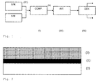
- the invention relates to a method for manufacturing a composition as described herein (c.f. fig.1 ), comprising the steps of (a) providing a homogeneous solvent composition (S.M), (b) providing nanoparticles (S.M)(c) combining said nanoparticles with said homogeneous solvent composition to obtain a suspension (COMP.).
- WO 3 nanoparticles were synthesized by flame spray synthesis.
- 42g of sodium metatungstate (Fluka) was dissolved in 750g distilled water and 75g acetic acid. After adding 225g aniline the solution was manually shaken for 3 min and washed twice with water in order to remove sodium and acetic acid. The obtained solution was diluted with THF 1:2 by weight.
- the precursor then was fed (5 ml min -1 , HNP Mikrosysteme, micro annular gear pump mzr-2900) to a spray nozzle, dispersed by oxygen (7 1 min -1 , PanGas tech.) and ignited by a premixed methane-oxygen flame (CH 4 : 1.2 1 min -1 , O 2 : 2.2 1 min -1 ) .
- the off-gas was filtered through a glass fiber filter (Schleicher&Schuell) by a vacuum pump (Busch, Seco SV1040CV) at about 20 m 3 h -1 .
- the obtained blue WO 3 nanopowder was collected from the glass fiber filter.
- Example 1 For the preparation of the WO 3 suspension 4 wt% of WO 3 nanopowder was dispersed in a mixture of 10 wt% distilled water, 90 wt% dry ethanol and 5 wt% butoxyethanol. The finally prepared dispersion is transparent and stable for more than 3 months. Drying of the obtained dispersion at about 150°C resulted in a residual carbon content (microanalysis) of below 2 wt%.
- WO 3 nanoparticle films were spin-coated on HDPE and PVC foils resulting in highly transparent WO 3 films. The thickness of the deposited WO 3 films was determined as ⁇ 50nm by scanning electron microscopy (SEM). The surface roughness was estimated to be in the range of 20nm (SEM).
- Example 2 An electrostatically stabilized WO 3 suspension was obtained by using 85 wt% ethanol, 5 wt% of propoxyethanol, 4 wt% of WO 3 (as described above) and 6 wt% of water without the use of an organic surfactant or dispersing agent. After dispersion application the coated material is dried at approx. 150 °C. During drying, the ethanol evaporates first, leaving back water, WO 3 and propoxyethanol. (It is believed propoxyethanol prevents de-wetting of the still wet film composed of water and WO 3 .) Next, water evaporates prior leaving a wet film of WO 3 and propoxyethanol only.
- WO 3 and propoxyethanol is not a stable dispersion system, but the film drying at this stage is almost complete and WO 3 has no time to form loose agglomerates. As a result, a thin film with a thickness below 100 nm and a surface roughness below 100 nm is obtained, free of residual organic materials.
- Examples 3-15 According to ex. 1, the following examples are prepared using the respective starting materials, whereby examples 3 - 7 are for comparative purposes.
- Suspension stability (#) Wettability (##) 3* 5% 0% 95% ethanol 0% very low n.a.
- Examples 1, 8, 10 - 15 also show good wettability on PVC foils.
- the inventive suspensions show good wettability on hydrophobic substrates. It was also observed that none of the suspensions according to ex. 1 - 15 damages PVC or HDPE foils. Thus, the solvent combination used in the inventive suspensions, does not damage organic electronic substrates.
- the films obtained according to ex. 8, 10 - 15 are dried in Air (150°C).
- the thus obtained films have a thickness below 100 nm, are defect free and a surface roughness below 100 nm (all as determined by microscopy). Further, the thus obtained films have less than 2.5 wt% organic residuals within the film. For these dried films, further processing is possible without further purification. Thus, no cleaning step - such as plasma or ozone treatment - of the as-deposited films is required.
Landscapes
- Engineering & Computer Science (AREA)
- Manufacturing & Machinery (AREA)
- Physics & Mathematics (AREA)
- Electromagnetism (AREA)
- Optics & Photonics (AREA)
- Electroluminescent Light Sources (AREA)
- Photovoltaic Devices (AREA)
Priority Applications (1)
| Application Number | Priority Date | Filing Date | Title |
|---|---|---|---|
| EP12772194.2A EP2771920B1 (en) | 2011-10-28 | 2012-10-10 | Solution-processable tungsten oxide buffer layers and organic electronics comprising same |
Applications Claiming Priority (3)
| Application Number | Priority Date | Filing Date | Title |
|---|---|---|---|
| EP11008644 | 2011-10-28 | ||
| PCT/CH2012/000234 WO2013059948A1 (en) | 2011-10-28 | 2012-10-10 | Solution-processable tungsten oxide buffer layers and organic electronics comprising same |
| EP12772194.2A EP2771920B1 (en) | 2011-10-28 | 2012-10-10 | Solution-processable tungsten oxide buffer layers and organic electronics comprising same |
Publications (2)
| Publication Number | Publication Date |
|---|---|
| EP2771920A1 EP2771920A1 (en) | 2014-09-03 |
| EP2771920B1 true EP2771920B1 (en) | 2016-08-24 |
Family
ID=47017984
Family Applications (1)
| Application Number | Title | Priority Date | Filing Date |
|---|---|---|---|
| EP12772194.2A Active EP2771920B1 (en) | 2011-10-28 | 2012-10-10 | Solution-processable tungsten oxide buffer layers and organic electronics comprising same |
Country Status (5)
| Country | Link |
|---|---|
| EP (1) | EP2771920B1 (enExample) |
| JP (1) | JP6214539B2 (enExample) |
| KR (1) | KR101996107B1 (enExample) |
| CN (1) | CN103988330B (enExample) |
| WO (1) | WO2013059948A1 (enExample) |
Families Citing this family (4)
| Publication number | Priority date | Publication date | Assignee | Title |
|---|---|---|---|---|
| TWI523919B (zh) * | 2014-12-04 | 2016-03-01 | 財團法人工業技術研究院 | 具有防霧與隔熱功能之塗料組成物、其製法及薄膜 |
| US11462711B2 (en) * | 2017-06-26 | 2022-10-04 | Samsung Display Co., Ltd. | Light-emitting device and method of fabricating display panel therewith |
| CN110350091A (zh) * | 2019-07-02 | 2019-10-18 | 上海大学 | 有机光电探测器及其制备方法 |
| CN116354399B (zh) * | 2023-06-02 | 2023-08-04 | 崇义章源钨业股份有限公司 | 一种制备松散纳米氧化钨的方法 |
Family Cites Families (8)
| Publication number | Priority date | Publication date | Assignee | Title |
|---|---|---|---|---|
| JP3400530B2 (ja) * | 1994-04-18 | 2003-04-28 | 三菱化学株式会社 | 耐摩耗性被覆組成物 |
| JP2002373785A (ja) * | 2001-06-15 | 2002-12-26 | Canon Inc | 発光素子及び表示装置 |
| US7880038B2 (en) * | 2003-04-18 | 2011-02-01 | Sumitomo Chemical Company, Limited | Metal catalyst and its use |
| EP2843675A3 (en) * | 2004-01-22 | 2015-04-01 | Showa Denko K.K. | Metal oxide dispersion, metal oxide electrode film, and dye sensitized solar cell |
| JP4799881B2 (ja) | 2004-12-27 | 2011-10-26 | 三井金属鉱業株式会社 | 導電性インク |
| JP2008041894A (ja) * | 2006-08-04 | 2008-02-21 | Matsushita Electric Ind Co Ltd | 有機エレクトロルミネッセント素子およびその製造方法 |
| WO2009110234A1 (ja) | 2008-03-04 | 2009-09-11 | 株式会社 東芝 | 水系分散液とそれを用いた塗料、膜および製品 |
| JP2011005475A (ja) * | 2009-05-29 | 2011-01-13 | Sumitomo Chemical Co Ltd | 光触媒体分散液およびそれを用いた光触媒機能製品 |
-
2012
- 2012-10-10 CN CN201280060498.XA patent/CN103988330B/zh active Active
- 2012-10-10 KR KR1020147013990A patent/KR101996107B1/ko active Active
- 2012-10-10 JP JP2014537439A patent/JP6214539B2/ja active Active
- 2012-10-10 EP EP12772194.2A patent/EP2771920B1/en active Active
- 2012-10-10 WO PCT/CH2012/000234 patent/WO2013059948A1/en not_active Ceased
Also Published As
| Publication number | Publication date |
|---|---|
| CN103988330B (zh) | 2016-08-24 |
| JP6214539B2 (ja) | 2017-10-18 |
| KR20140085551A (ko) | 2014-07-07 |
| KR101996107B1 (ko) | 2019-07-03 |
| EP2771920A1 (en) | 2014-09-03 |
| WO2013059948A1 (en) | 2013-05-02 |
| JP2015501540A (ja) | 2015-01-15 |
| CN103988330A (zh) | 2014-08-13 |
Similar Documents
| Publication | Publication Date | Title |
|---|---|---|
| KR102120534B1 (ko) | 용액-가공성 금속 산화물 완충 층을 포함하는 광전자 장치 | |
| Sankaran et al. | Fabrication of polymer solar cells from organic nanoparticle dispersions by doctor blading or ink-jet printing | |
| CN104245124B (zh) | 可溶液加工的氧化钨缓冲层和包括其的电子器件 | |
| US20160351808A1 (en) | Electronic devices comprising solution-processable metal oxide buffer layers | |
| Xu et al. | A wide temperature tolerance, solution-processed MoOx interface layer for efficient and stable organic solar cells | |
| CN105778619A (zh) | 聚合物-纳米金属氧化物复合墨水及其制备方法与应用 | |
| WO2015169243A1 (zh) | 金属氧化物-导电聚合物-醇组合物、其制备方法及应用 | |
| TWI608628B (zh) | 光伏系統及用於製造光伏系統之噴塗方法 | |
| WO2016095828A1 (zh) | 聚合物-金属化合物复合墨水及其制备方法与应用 | |
| CN103403906A (zh) | 光伏电池 | |
| EP2771920B1 (en) | Solution-processable tungsten oxide buffer layers and organic electronics comprising same | |
| US11139433B2 (en) | Tungstate ion solution and hybrid photovoltaic device | |
| WO2026073344A1 (en) | Semiconductor device comprising mxene composite material and related method | |
| HK1189711A (zh) | 光伏电池 |
Legal Events
| Date | Code | Title | Description |
|---|---|---|---|
| PUAI | Public reference made under article 153(3) epc to a published international application that has entered the european phase |
Free format text: ORIGINAL CODE: 0009012 |
|
| 17P | Request for examination filed |
Effective date: 20140428 |
|
| AK | Designated contracting states |
Kind code of ref document: A1 Designated state(s): AL AT BE BG CH CY CZ DE DK EE ES FI FR GB GR HR HU IE IS IT LI LT LU LV MC MK MT NL NO PL PT RO RS SE SI SK SM TR |
|
| DAX | Request for extension of the european patent (deleted) | ||
| 17Q | First examination report despatched |
Effective date: 20150611 |
|
| GRAP | Despatch of communication of intention to grant a patent |
Free format text: ORIGINAL CODE: EPIDOSNIGR1 |
|
| INTG | Intention to grant announced |
Effective date: 20160504 |
|
| GRAS | Grant fee paid |
Free format text: ORIGINAL CODE: EPIDOSNIGR3 |
|
| GRAA | (expected) grant |
Free format text: ORIGINAL CODE: 0009210 |
|
| AK | Designated contracting states |
Kind code of ref document: B1 Designated state(s): AL AT BE BG CH CY CZ DE DK EE ES FI FR GB GR HR HU IE IS IT LI LT LU LV MC MK MT NL NO PL PT RO RS SE SI SK SM TR |
|
| REG | Reference to a national code |
Ref country code: GB Ref legal event code: FG4D |
|
| REG | Reference to a national code |
Ref country code: CH Ref legal event code: NV Representative=s name: E. BLUM AND CO. AG PATENT- UND MARKENANWAELTE , CH Ref country code: CH Ref legal event code: EP |
|
| REG | Reference to a national code |
Ref country code: AT Ref legal event code: REF Ref document number: 823768 Country of ref document: AT Kind code of ref document: T Effective date: 20160915 |
|
| REG | Reference to a national code |
Ref country code: IE Ref legal event code: FG4D |
|
| REG | Reference to a national code |
Ref country code: DE Ref legal event code: R096 Ref document number: 602012022244 Country of ref document: DE |
|
| REG | Reference to a national code |
Ref country code: FR Ref legal event code: PLFP Year of fee payment: 5 |
|
| REG | Reference to a national code |
Ref country code: LT Ref legal event code: MG4D |
|
| REG | Reference to a national code |
Ref country code: NL Ref legal event code: MP Effective date: 20160824 |
|
| REG | Reference to a national code |
Ref country code: AT Ref legal event code: MK05 Ref document number: 823768 Country of ref document: AT Kind code of ref document: T Effective date: 20160824 |
|
| PG25 | Lapsed in a contracting state [announced via postgrant information from national office to epo] |
Ref country code: RS Free format text: LAPSE BECAUSE OF FAILURE TO SUBMIT A TRANSLATION OF THE DESCRIPTION OR TO PAY THE FEE WITHIN THE PRESCRIBED TIME-LIMIT Effective date: 20160824 Ref country code: HR Free format text: LAPSE BECAUSE OF FAILURE TO SUBMIT A TRANSLATION OF THE DESCRIPTION OR TO PAY THE FEE WITHIN THE PRESCRIBED TIME-LIMIT Effective date: 20160824 Ref country code: NL Free format text: LAPSE BECAUSE OF FAILURE TO SUBMIT A TRANSLATION OF THE DESCRIPTION OR TO PAY THE FEE WITHIN THE PRESCRIBED TIME-LIMIT Effective date: 20160824 Ref country code: LT Free format text: LAPSE BECAUSE OF FAILURE TO SUBMIT A TRANSLATION OF THE DESCRIPTION OR TO PAY THE FEE WITHIN THE PRESCRIBED TIME-LIMIT Effective date: 20160824 Ref country code: FI Free format text: LAPSE BECAUSE OF FAILURE TO SUBMIT A TRANSLATION OF THE DESCRIPTION OR TO PAY THE FEE WITHIN THE PRESCRIBED TIME-LIMIT Effective date: 20160824 Ref country code: IT Free format text: LAPSE BECAUSE OF FAILURE TO SUBMIT A TRANSLATION OF THE DESCRIPTION OR TO PAY THE FEE WITHIN THE PRESCRIBED TIME-LIMIT Effective date: 20160824 Ref country code: NO Free format text: LAPSE BECAUSE OF FAILURE TO SUBMIT A TRANSLATION OF THE DESCRIPTION OR TO PAY THE FEE WITHIN THE PRESCRIBED TIME-LIMIT Effective date: 20161124 |
|
| PG25 | Lapsed in a contracting state [announced via postgrant information from national office to epo] |
Ref country code: BE Free format text: LAPSE BECAUSE OF NON-PAYMENT OF DUE FEES Effective date: 20161031 Ref country code: SE Free format text: LAPSE BECAUSE OF FAILURE TO SUBMIT A TRANSLATION OF THE DESCRIPTION OR TO PAY THE FEE WITHIN THE PRESCRIBED TIME-LIMIT Effective date: 20160824 Ref country code: PT Free format text: LAPSE BECAUSE OF FAILURE TO SUBMIT A TRANSLATION OF THE DESCRIPTION OR TO PAY THE FEE WITHIN THE PRESCRIBED TIME-LIMIT Effective date: 20161226 Ref country code: ES Free format text: LAPSE BECAUSE OF FAILURE TO SUBMIT A TRANSLATION OF THE DESCRIPTION OR TO PAY THE FEE WITHIN THE PRESCRIBED TIME-LIMIT Effective date: 20160824 Ref country code: LV Free format text: LAPSE BECAUSE OF FAILURE TO SUBMIT A TRANSLATION OF THE DESCRIPTION OR TO PAY THE FEE WITHIN THE PRESCRIBED TIME-LIMIT Effective date: 20160824 Ref country code: AT Free format text: LAPSE BECAUSE OF FAILURE TO SUBMIT A TRANSLATION OF THE DESCRIPTION OR TO PAY THE FEE WITHIN THE PRESCRIBED TIME-LIMIT Effective date: 20160824 Ref country code: GR Free format text: LAPSE BECAUSE OF FAILURE TO SUBMIT A TRANSLATION OF THE DESCRIPTION OR TO PAY THE FEE WITHIN THE PRESCRIBED TIME-LIMIT Effective date: 20161125 |
|
| REG | Reference to a national code |
Ref country code: CH Ref legal event code: PFA Owner name: AVANTAMA AG, CH Free format text: FORMER OWNER: NANOGRADE AG, CH |
|
| PG25 | Lapsed in a contracting state [announced via postgrant information from national office to epo] |
Ref country code: RO Free format text: LAPSE BECAUSE OF FAILURE TO SUBMIT A TRANSLATION OF THE DESCRIPTION OR TO PAY THE FEE WITHIN THE PRESCRIBED TIME-LIMIT Effective date: 20160824 Ref country code: EE Free format text: LAPSE BECAUSE OF FAILURE TO SUBMIT A TRANSLATION OF THE DESCRIPTION OR TO PAY THE FEE WITHIN THE PRESCRIBED TIME-LIMIT Effective date: 20160824 |
|
| REG | Reference to a national code |
Ref country code: DE Ref legal event code: R081 Ref document number: 602012022244 Country of ref document: DE Owner name: AVANTAMA AG, CH Free format text: FORMER OWNER: NANOGRADE AG, STAEFA, CH |
|
| REG | Reference to a national code |
Ref country code: DE Ref legal event code: R097 Ref document number: 602012022244 Country of ref document: DE |
|
| PG25 | Lapsed in a contracting state [announced via postgrant information from national office to epo] |
Ref country code: DK Free format text: LAPSE BECAUSE OF FAILURE TO SUBMIT A TRANSLATION OF THE DESCRIPTION OR TO PAY THE FEE WITHIN THE PRESCRIBED TIME-LIMIT Effective date: 20160824 Ref country code: SK Free format text: LAPSE BECAUSE OF FAILURE TO SUBMIT A TRANSLATION OF THE DESCRIPTION OR TO PAY THE FEE WITHIN THE PRESCRIBED TIME-LIMIT Effective date: 20160824 Ref country code: SM Free format text: LAPSE BECAUSE OF FAILURE TO SUBMIT A TRANSLATION OF THE DESCRIPTION OR TO PAY THE FEE WITHIN THE PRESCRIBED TIME-LIMIT Effective date: 20160824 Ref country code: BG Free format text: LAPSE BECAUSE OF FAILURE TO SUBMIT A TRANSLATION OF THE DESCRIPTION OR TO PAY THE FEE WITHIN THE PRESCRIBED TIME-LIMIT Effective date: 20161124 Ref country code: BE Free format text: LAPSE BECAUSE OF FAILURE TO SUBMIT A TRANSLATION OF THE DESCRIPTION OR TO PAY THE FEE WITHIN THE PRESCRIBED TIME-LIMIT Effective date: 20160824 Ref country code: CZ Free format text: LAPSE BECAUSE OF FAILURE TO SUBMIT A TRANSLATION OF THE DESCRIPTION OR TO PAY THE FEE WITHIN THE PRESCRIBED TIME-LIMIT Effective date: 20160824 Ref country code: PL Free format text: LAPSE BECAUSE OF FAILURE TO SUBMIT A TRANSLATION OF THE DESCRIPTION OR TO PAY THE FEE WITHIN THE PRESCRIBED TIME-LIMIT Effective date: 20160824 |
|
| PLBE | No opposition filed within time limit |
Free format text: ORIGINAL CODE: 0009261 |
|
| STAA | Information on the status of an ep patent application or granted ep patent |
Free format text: STATUS: NO OPPOSITION FILED WITHIN TIME LIMIT |
|
| REG | Reference to a national code |
Ref country code: IE Ref legal event code: MM4A |
|
| 26N | No opposition filed |
Effective date: 20170526 |
|
| PG25 | Lapsed in a contracting state [announced via postgrant information from national office to epo] |
Ref country code: LU Free format text: LAPSE BECAUSE OF NON-PAYMENT OF DUE FEES Effective date: 20161010 Ref country code: SI Free format text: LAPSE BECAUSE OF FAILURE TO SUBMIT A TRANSLATION OF THE DESCRIPTION OR TO PAY THE FEE WITHIN THE PRESCRIBED TIME-LIMIT Effective date: 20160824 |
|
| REG | Reference to a national code |
Ref country code: FR Ref legal event code: PLFP Year of fee payment: 6 |
|
| PG25 | Lapsed in a contracting state [announced via postgrant information from national office to epo] |
Ref country code: IE Free format text: LAPSE BECAUSE OF NON-PAYMENT OF DUE FEES Effective date: 20161010 |
|
| PG25 | Lapsed in a contracting state [announced via postgrant information from national office to epo] |
Ref country code: HU Free format text: LAPSE BECAUSE OF FAILURE TO SUBMIT A TRANSLATION OF THE DESCRIPTION OR TO PAY THE FEE WITHIN THE PRESCRIBED TIME-LIMIT; INVALID AB INITIO Effective date: 20121010 |
|
| PG25 | Lapsed in a contracting state [announced via postgrant information from national office to epo] |
Ref country code: CY Free format text: LAPSE BECAUSE OF FAILURE TO SUBMIT A TRANSLATION OF THE DESCRIPTION OR TO PAY THE FEE WITHIN THE PRESCRIBED TIME-LIMIT Effective date: 20160824 Ref country code: IS Free format text: LAPSE BECAUSE OF FAILURE TO SUBMIT A TRANSLATION OF THE DESCRIPTION OR TO PAY THE FEE WITHIN THE PRESCRIBED TIME-LIMIT Effective date: 20160824 Ref country code: MK Free format text: LAPSE BECAUSE OF FAILURE TO SUBMIT A TRANSLATION OF THE DESCRIPTION OR TO PAY THE FEE WITHIN THE PRESCRIBED TIME-LIMIT Effective date: 20160824 Ref country code: MT Free format text: LAPSE BECAUSE OF NON-PAYMENT OF DUE FEES Effective date: 20161031 Ref country code: MC Free format text: LAPSE BECAUSE OF FAILURE TO SUBMIT A TRANSLATION OF THE DESCRIPTION OR TO PAY THE FEE WITHIN THE PRESCRIBED TIME-LIMIT Effective date: 20160824 |
|
| REG | Reference to a national code |
Ref country code: FR Ref legal event code: PLFP Year of fee payment: 7 |
|
| PG25 | Lapsed in a contracting state [announced via postgrant information from national office to epo] |
Ref country code: TR Free format text: LAPSE BECAUSE OF FAILURE TO SUBMIT A TRANSLATION OF THE DESCRIPTION OR TO PAY THE FEE WITHIN THE PRESCRIBED TIME-LIMIT Effective date: 20160824 Ref country code: AL Free format text: LAPSE BECAUSE OF FAILURE TO SUBMIT A TRANSLATION OF THE DESCRIPTION OR TO PAY THE FEE WITHIN THE PRESCRIBED TIME-LIMIT Effective date: 20160824 |
|
| REG | Reference to a national code |
Ref country code: DE Ref legal event code: R079 Ref document number: 602012022244 Country of ref document: DE Free format text: PREVIOUS MAIN CLASS: H01L0051520000 Ipc: H10K0050800000 |
|
| REG | Reference to a national code |
Ref country code: CH Ref legal event code: U11 Free format text: ST27 STATUS EVENT CODE: U-0-0-U10-U11 (AS PROVIDED BY THE NATIONAL OFFICE) Effective date: 20251101 |
|
| PGFP | Annual fee paid to national office [announced via postgrant information from national office to epo] |
Ref country code: DE Payment date: 20251021 Year of fee payment: 14 |
|
| PGFP | Annual fee paid to national office [announced via postgrant information from national office to epo] |
Ref country code: GB Payment date: 20251022 Year of fee payment: 14 |
|
| PGFP | Annual fee paid to national office [announced via postgrant information from national office to epo] |
Ref country code: FR Payment date: 20251030 Year of fee payment: 14 |
|
| PGFP | Annual fee paid to national office [announced via postgrant information from national office to epo] |
Ref country code: CH Payment date: 20251101 Year of fee payment: 14 |