EP2770538A1 - Fin type semiconductor structure suitable for producing esd protection device - Google Patents
Fin type semiconductor structure suitable for producing esd protection device Download PDFInfo
- Publication number
- EP2770538A1 EP2770538A1 EP13156607.7A EP13156607A EP2770538A1 EP 2770538 A1 EP2770538 A1 EP 2770538A1 EP 13156607 A EP13156607 A EP 13156607A EP 2770538 A1 EP2770538 A1 EP 2770538A1
- Authority
- EP
- European Patent Office
- Prior art keywords
- fins
- doping type
- doping
- top portion
- type
- Prior art date
- Legal status (The legal status is an assumption and is not a legal conclusion. Google has not performed a legal analysis and makes no representation as to the accuracy of the status listed.)
- Withdrawn
Links
- 239000004065 semiconductor Substances 0.000 title claims abstract description 36
- 239000000758 substrate Substances 0.000 claims abstract description 22
- 238000004519 manufacturing process Methods 0.000 claims abstract description 13
- 239000002184 metal Substances 0.000 claims description 16
- 238000000034 method Methods 0.000 claims description 16
- 239000000463 material Substances 0.000 claims description 12
- 239000003989 dielectric material Substances 0.000 claims description 9
- 238000002955 isolation Methods 0.000 claims description 3
- 238000005516 engineering process Methods 0.000 abstract description 3
- 239000002019 doping agent Substances 0.000 description 10
- XUIMIQQOPSSXEZ-UHFFFAOYSA-N Silicon Chemical compound [Si] XUIMIQQOPSSXEZ-UHFFFAOYSA-N 0.000 description 5
- VYPSYNLAJGMNEJ-UHFFFAOYSA-N Silicium dioxide Chemical compound O=[Si]=O VYPSYNLAJGMNEJ-UHFFFAOYSA-N 0.000 description 4
- 229910052710 silicon Inorganic materials 0.000 description 4
- 239000010703 silicon Substances 0.000 description 4
- 238000001465 metallisation Methods 0.000 description 2
- 229910052814 silicon oxide Inorganic materials 0.000 description 2
- 239000002800 charge carrier Substances 0.000 description 1
- 229910052681 coesite Inorganic materials 0.000 description 1
- 238000010276 construction Methods 0.000 description 1
- 229910052906 cristobalite Inorganic materials 0.000 description 1
- 230000001419 dependent effect Effects 0.000 description 1
- 238000005530 etching Methods 0.000 description 1
- 239000007943 implant Substances 0.000 description 1
- 238000000926 separation method Methods 0.000 description 1
- 239000000377 silicon dioxide Substances 0.000 description 1
- 239000007787 solid Substances 0.000 description 1
- 229910052682 stishovite Inorganic materials 0.000 description 1
- 229910052905 tridymite Inorganic materials 0.000 description 1
Images


Classifications
-
- H—ELECTRICITY
- H10—SEMICONDUCTOR DEVICES; ELECTRIC SOLID-STATE DEVICES NOT OTHERWISE PROVIDED FOR
- H10D—INORGANIC ELECTRIC SEMICONDUCTOR DEVICES
- H10D8/00—Diodes
- H10D8/01—Manufacture or treatment
-
- H—ELECTRICITY
- H10—SEMICONDUCTOR DEVICES; ELECTRIC SOLID-STATE DEVICES NOT OTHERWISE PROVIDED FOR
- H10D—INORGANIC ELECTRIC SEMICONDUCTOR DEVICES
- H10D62/00—Semiconductor bodies, or regions thereof, of devices having potential barriers
- H10D62/10—Shapes, relative sizes or dispositions of the regions of the semiconductor bodies; Shapes of the semiconductor bodies
- H10D62/113—Isolations within a component, i.e. internal isolations
- H10D62/115—Dielectric isolations, e.g. air gaps
-
- H—ELECTRICITY
- H10—SEMICONDUCTOR DEVICES; ELECTRIC SOLID-STATE DEVICES NOT OTHERWISE PROVIDED FOR
- H10D—INORGANIC ELECTRIC SEMICONDUCTOR DEVICES
- H10D8/00—Diodes
- H10D8/01—Manufacture or treatment
- H10D8/041—Manufacture or treatment of multilayer diodes
-
- H—ELECTRICITY
- H10—SEMICONDUCTOR DEVICES; ELECTRIC SOLID-STATE DEVICES NOT OTHERWISE PROVIDED FOR
- H10D—INORGANIC ELECTRIC SEMICONDUCTOR DEVICES
- H10D8/00—Diodes
- H10D8/422—PN diodes having the PN junctions in mesas
-
- H—ELECTRICITY
- H10—SEMICONDUCTOR DEVICES; ELECTRIC SOLID-STATE DEVICES NOT OTHERWISE PROVIDED FOR
- H10D—INORGANIC ELECTRIC SEMICONDUCTOR DEVICES
- H10D8/00—Diodes
- H10D8/80—PNPN diodes, e.g. Shockley diodes or break-over diodes
-
- H—ELECTRICITY
- H10—SEMICONDUCTOR DEVICES; ELECTRIC SOLID-STATE DEVICES NOT OTHERWISE PROVIDED FOR
- H10D—INORGANIC ELECTRIC SEMICONDUCTOR DEVICES
- H10D89/00—Aspects of integrated devices not covered by groups H10D84/00 - H10D88/00
- H10D89/60—Integrated devices comprising arrangements for electrical or thermal protection, e.g. protection circuits against electrostatic discharge [ESD]
- H10D89/601—Integrated devices comprising arrangements for electrical or thermal protection, e.g. protection circuits against electrostatic discharge [ESD] for devices having insulated gate electrodes, e.g. for IGFETs or IGBTs
- H10D89/611—Integrated devices comprising arrangements for electrical or thermal protection, e.g. protection circuits against electrostatic discharge [ESD] for devices having insulated gate electrodes, e.g. for IGFETs or IGBTs using diodes as protective elements
-
- H—ELECTRICITY
- H10—SEMICONDUCTOR DEVICES; ELECTRIC SOLID-STATE DEVICES NOT OTHERWISE PROVIDED FOR
- H10D—INORGANIC ELECTRIC SEMICONDUCTOR DEVICES
- H10D89/00—Aspects of integrated devices not covered by groups H10D84/00 - H10D88/00
- H10D89/60—Integrated devices comprising arrangements for electrical or thermal protection, e.g. protection circuits against electrostatic discharge [ESD]
- H10D89/601—Integrated devices comprising arrangements for electrical or thermal protection, e.g. protection circuits against electrostatic discharge [ESD] for devices having insulated gate electrodes, e.g. for IGFETs or IGBTs
- H10D89/711—Integrated devices comprising arrangements for electrical or thermal protection, e.g. protection circuits against electrostatic discharge [ESD] for devices having insulated gate electrodes, e.g. for IGFETs or IGBTs using bipolar transistors as protective elements
- H10D89/713—Integrated devices comprising arrangements for electrical or thermal protection, e.g. protection circuits against electrostatic discharge [ESD] for devices having insulated gate electrodes, e.g. for IGFETs or IGBTs using bipolar transistors as protective elements including a PNP transistor and a NPN transistor, wherein each of said transistors has its base region coupled to the collector region of the other transistor, e.g. silicon controlled rectifier [SCR] devices
-
- H—ELECTRICITY
- H10—SEMICONDUCTOR DEVICES; ELECTRIC SOLID-STATE DEVICES NOT OTHERWISE PROVIDED FOR
- H10D—INORGANIC ELECTRIC SEMICONDUCTOR DEVICES
- H10D62/00—Semiconductor bodies, or regions thereof, of devices having potential barriers
- H10D62/10—Shapes, relative sizes or dispositions of the regions of the semiconductor bodies; Shapes of the semiconductor bodies
- H10D62/124—Shapes, relative sizes or dispositions of the regions of semiconductor bodies or of junctions between the regions
- H10D62/126—Top-view geometrical layouts of the regions or the junctions
Definitions
- the present invention is related to the fabrication of semiconductor structures, applicable in an ESD protection device.
- structures comprising p-n junctions between oppositely doped regions in a semiconductor substrate are essential for the construction of ESD (Electrostatic Discharge) protection devices.
- ESD Electrostatic Discharge
- the invention is related to structures, devices and production methods as described in the appended claims, which answer to the above-described need.
- the present invention is related to a semiconductor structure suitable for producing an Electrostatic Discharge (ESD) protection device, the structure comprising a plurality of fins on a substrate region of a first doping type.
- the fins have a base portion of said same first doping type (e.g. n-type), with at least one fin having a top portion of a second doping type (e.g. p-type), so that a p-n junction extends over the entire length of said at least one fin.
- the plurality of fins comprises a number of a p-fins and a number of n-fins, arranged in alternating fashion or in separate groups of p and n fins, preferably with a larger distance between the groups than between neighbouring fins in the group.
- the structure can be applied in the production of any known type of ESD protection device, facilitating the production of such devices in a fin-based technology.
- the invention is equally related to ESD devices as such comprising the structure of the invention and to methods for producing the structure.
- the invention is in particular related to a semiconductor structure comprising :
- said fins may have alternating top portions of the first and second doping type.
- said fins are grouped in one or more first groups of fins having a top portion of the first doping type and one or more second groups of fins having a top portion of the second doping type.
- the distance between two groups of fins having top portions of opposite doping types may be larger than the distance between two individual fins in each of said groups.
- the invention is equally related to a semiconductor device comprising :
- said first and second contact means may comprise metal-filled contact vias and metal lines separated by intermetal dielectric material.
- a separating layer may be present, covering the top and at least part of the side surfaces of said top portions of the fins, in the areas between said contact vias said separating layer comprising at least a dielectric layer in contact with said top and side surfaces.
- the device of the invention may be a diode.
- the device of the invention may be an Electrostatic Discharge protection device.
- the invention is equally related to a method for producing a semiconductor structure comprising the steps of :
- said second and third doping steps are performed so as to obtain alternating top portions of the first and second doping type.
- said second and third doping steps are performed so as to obtain one or more first groups of fins having a top portion of the first doping type and one or more second groups of fins having a top portion of the second doping type.
- the distance between two groups of fins having top portions of opposite doping types is larger than the distance between two individual fins in each of said groups.
- the invention is equally related to a method for producing a semiconductor device, comprising the steps of :
- said first and second contact means comprise metal-filled contact vias and metal lines separated by intermetal dielectric material.
- the latter embodiment may further comprise the step of producing a separating layer, said layer covering the top and at least part of the side surfaces of said top portions of the fins, in the areas between said contact vias, said separating layer comprising at least a dielectric layer in contact with said top and side surfaces.
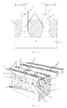
- Figure 1 illustrates a schematic image of a diode structure according to the invention comprising two fins. In reality the structure is likely to comprise more than two fins.
- Figure 2 shows a 3D-image of a diode according to the invention comprising multiple fins, including a contact structure obtainable by standard BEOL techniques.
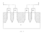
- Figure 3 shows an embodiment comprising multiple fins grouped together in groups of p and n-type fins respectively.
- Figures 4a to 4g illustrate a method for producing a structure according to the invention.
- Figure 5 illustrates an SCR type device for ESD protection, incorporating semiconductor structures according to the invention.
- a 'diode structure' is defined as a semiconductor structure suitable for producing a diode by electrically connecting said structure to a cathode and anode terminal.
- the diode structure is thus basically a structure comprising a p-n junction between oppositely doped regions, and suitable for being contacted so that a current may run through said junction depending on the external voltage between cathode and anode.
- the invention is not limited to diodes as such.
- the diode structure may be contacted in other ways than the way described above, or may be part of a larger device, such as various types of ESD protection devices, see further.
- a diode structure comprises at least two mutually parallel fin-shaped structures 1 and 2 (hereafter referred to as 'fins'), placed on a common base substrate 3.
- the base substrate consists of a semiconductor material of a first doping type, for example n-doped silicon in the embodiment shown in figure 1 .
- the base substrate 3 can be a portion of a larger substrate, e.g. an n-well in a p-doped silicon wafer.
- the fins have a base portion 4 and top portions 5 and 6.
- the base portions are n-doped, like the base substrate 3.
- the base portions are integral with the base substrate, i.e.
- the top portions 5 and 6 of the fins are respectively n+ doped and p+ doped (the '+' indicating high dopant density).
- the fins are embedded in a layer 7 of dielectric material, for example SiO 2 , with at least part of the top portions 5/6 extending outwards with respect to said layer 7.
- the dopant density for region 4 is between 1e16cm -3 and 2e18cm -3 , more preferably between 1e17cm -3 and 5e17cm -3 .
- the dopant density for the n+ and p+ regions 5 and 6 may be between 5e19cm -3 and 5e21cm -3 , more preferably between 2e20cm -3 and 6e20cm -3 .
- each base portion 4 and each top portion 5/6 of the fins is doped by the same dopant type over its entire length (i.e. perpendicular to the drawing of figure 1 ).
- the p-n junction 8 in the second fin 2 which defines the diode when the structure is connected to cathode and anode terminals C and A, is a horizontal junction between a top portion 6 that is p+ doped and a base portion 4 that is n-doped.
- the n+ top portion 5 is required for obtaining a good ohmic contact for the charge carriers towards the contacts on top of the fins.
- Said contacts are shown only schematically by contact lines 9 leading to cathode and anode terminals C and A respectively (a more realistic version of the contact lines is shown hereafter).
- the top level of the dielectric layer 7 does not necessarily coincide with the position of the junction 8.
- the doping types described above and indicated in figure 1 may be reversed (p instead of n and n instead of p).
- a diode structure according to the invention comprises more than two fins.
- a structure of this type is shown in figure 2 , which is a 3-D picture of a diode according to the invention, including a metallization structure for contacting the diode.
- Five fins are shown on an n-type base substrate 10, each having an n-doped base portion 11 and alternately provided with p+ and n+ doped top portions 12.
- the base portions 11 are embedded in a dielectric layer 13, e.g. a silicon oxide.
- Metal-filled vias 14 are provided on top of the p+ top portions 12, and interconnected by metal lines 15.
- Further metal-filled vias 16 are provided on top of the n+ top portions 12 and interconnected by higher level metal lines 17.
- the vias and metal lines are separated from each other by intermetal dielectric layers (not shown), and can be produced according to known metallization techniques, known as BEOL (Back-end-of-line) processing.
- separating layers 20 are present in between the contact vias 14 on the p+ fins and in between contact vias 16 on the n+ fins.
- These layers 20 are formed of a dielectric material or at least comprise a dielectric material in contact with the fins.
- the layers 20 could have the structure of a gate stack : a dielectric layer covered by a metal layer, the dielectric isolating the fin from the metal.
- the layers 20 are covering the top and side surface of the fins' top portions 12, both the n+ and the p+ type top portions 12. The reason for these layers 20 is to avoid shorting neighbouring top portions 12 of different doping types when these top portions are subjected to Selective Epitaxial Growth (SEG).
- SEG Selective Epitaxial Growth
- SEG is a known technique applied to source and drain areas of FinFET transistors in order to decrease the resistance of these areas.
- SEG consists basically in growing a semiconductor layer on the top portion 12 of the fins, growing outward from the side walls and top surface of said top portions.
- SEG is preferably applied on the fins of a diode structure according to the invention. The outward growth of the SEG material may cause neighbouring p+ and n+ fins to be shorted, which may be prevented by the layers 20.
- the layers 20 are shaped like gates of a finFET device, and may thus be produced by available processes for gate definition and processing.
- the layers 20 are an optional feature that can be applied as a way of avoiding the shorting of p+ and n+ fins in a structure according to the invention. Another way of avoiding the shorting of p+ and n+ fins is by putting them at a greater distance from each other, as illustrated by the embodiment of figure 1 as compared to figure 2 . The distance should be high enough to avoid contact between SEG-grown material on neighbouring fins.
- groups of n+ fins and p+ fins may be produced, as illustrated by the embodiment shown in figure 3 .
- the distance between the group of n+ fins and the group of p+ fins is higher than the distance between individual fins in each group. This is again for reasons of avoiding shorting as a consequence of SEG.
- the advantage of grouping together a number of fins of the same doping type is that no precautions must be taken against shorting by SEG in the space between two neighbouring fins in a single group.
- Another embodiment (not shown) has groups of p+ and n+ fins with no difference in the distance between the fins of each group and between two neighbouring groups, but with a gate-shaped separation layer 20 in between the groups for avoiding shorting by SEG.
- This embodiment and the one with alternating doping types for all fins as shown in figure 2 has the advantage that it allows to produce a maximum of fins on a particular wafer surface.
- Figure 4 illustrates a possible process for producing a diode structure according to the invention.
- the process starts from an undoped or lowly doped substrate 30, e.g. a silicon wafer, see figure 4a .
- a number of trenches filled with silicon oxide 31 are produced by a standard STI (Shallow Trench Isolation) technique, known as such in the art (see figure 4b ).
- the silicon structures in between the trenches are the fins 32 which are uniform with the bulk area 33.
- a first doping step is then performed, to create a first n-type doping level in the fins 32 and in the bulk area 33 underneath said fins, see figure 4c .
- the first doping step may be performed before the STI step.
- the dopant density for obtained in the first doping step (n or p) is between 1e16cm -3 and 2e18cm -3 , more preferably between 1e17cm -3 and 5e17cm -3 .
- a top portion of the oxide is then removed by a known etching technique while covering the fins by a mask (not shown), leading to the structure of figure 4d .
- a second doping step performed under circumstances for obtaining a higher dopant density than the first doping step wherein an n-type dopant is injected into a first group of fins, while the other fins are covered by a first mask 34.
- a third doping step is done by injecting p-type dopants into the remaining group of fins, while covering the first group by a mask 35.
- the third doping step is again performed under circumstances for obtaining a higher dopant density than the first doping step. This leads to the top portions of said remaining group being p-doped at a high doping level (p+) ( fig. 4f ).
- the order of the n+ and p+ implant steps may be reversed.
- the dopant density for the n+ and p+ regions obtained after the second and third doping steps may be between 5e19cm -3 and 5e21cm -3 , more preferably between 2e20cm -3 and 6e20cm -3 .
- the structure is obtained as shown in figure 4g , comprising the top portions 12 of alternating p+ and n+ type.
- Standard SEG and BEOL steps (not shown) are then performed for creating the metal vias and contact lines 14/16/15/17 shown in figure 2 .
- the layer 20 may be applied on top of the top portions 12 of the fins, before subjecting the fins to the standard SEG process.
- the diode structure of the invention may be applied in various ESD device structures.
- ESD protection devices such as Silicon Controlled rectifier (SCR) or Bipolar Junction Transistor (BJT)
- the planar structures may be replaced by fin-based structures according to the invention.
- FIG 5 shows a standard SCR device, produced with 2 diode structures 40 and 41 according to the invention.
- Any other existing SCR architecture or other ESD device may be produced in an analogue way.
- the description of a layer being deposited or produced 'on' another layer or substrate includes the options of
Landscapes
- Semiconductor Integrated Circuits (AREA)
Abstract
A semiconductor structure suitable for producing an Electrostatic Discharge (ESD) protection device, the structure comprising a plurality of fins on a substrate region of a first doping type. The fins have a base portion of said same first doping type (e.g. n-type), with at least one fin having a top portion of a second doping type (e.g. p-type), so that a p-n junction extends over the entire length of said at least one fin. The plurality of fins comprises a number of a p-fins and a number of n-fins, arranged in alternating fashion or in separate groups of p and n fins, preferably with a larger distance between the groups than between neighbouring fins in the group. The structure can be applied in the production of any known type of ESD protection device, facilitating the production of such devices in a fin-based technology.
Description
- The present invention is related to the fabrication of semiconductor structures, applicable in an ESD protection device.
- In semiconductor processing, structures comprising p-n junctions between oppositely doped regions in a semiconductor substrate are essential for the construction of ESD (Electrostatic Discharge) protection devices. There is an ongoing need for improving the process efficiency of these devices and for integrating the production of said structures into standard semiconductor processing technology, especially in the area of fin-type processing.
- The invention is related to structures, devices and production methods as described in the appended claims, which answer to the above-described need. The present invention is related to a semiconductor structure suitable for producing an Electrostatic Discharge (ESD) protection device, the structure comprising a plurality of fins on a substrate region of a first doping type. The fins have a base portion of said same first doping type (e.g. n-type), with at least one fin having a top portion of a second doping type (e.g. p-type), so that a p-n junction extends over the entire length of said at least one fin. According to preferred embodiments, the plurality of fins comprises a number of a p-fins and a number of n-fins, arranged in alternating fashion or in separate groups of p and n fins, preferably with a larger distance between the groups than between neighbouring fins in the group. The structure can be applied in the production of any known type of ESD protection device, facilitating the production of such devices in a fin-based technology. The invention is equally related to ESD devices as such comprising the structure of the invention and to methods for producing the structure.
- The invention is in particular related to a semiconductor structure comprising :
- A base substrate consisting of doped semiconductor material of a first doping type,
- A plurality of mutually parallel fins on said base substrate, each of said fins consisting of a base portion and a top portion, said portions extending over the entire length of the fin,
- dielectric material in the regions between each pair of neighbouring fins,
wherein :- said base portions consist of doped semiconductor material of said first doping type,
- the top portion of at least one of said fins consists of semiconductor material of a second doping type opposite to the first, forming a p-n junction with the base portion of said fin,
- the top portions of the remaining fins consist of semiconductor material of said first doping type.
- In the structure of the invention, said fins may have alternating top portions of the first and second doping type.
- According to another embodiment, said fins are grouped in one or more first groups of fins having a top portion of the first doping type and one or more second groups of fins having a top portion of the second doping type. In a particular embodiment, the distance between two groups of fins having top portions of opposite doping types may be larger than the distance between two individual fins in each of said groups.
- The invention is equally related to a semiconductor device comprising :
- a semiconductor structure according to the invention,
- first contact means for contacting all the fins having a top portion of the first doping type, and second contact means for contacting all the fins having a top portion of the second doping type.
- In a device according to the invention, said first and second contact means may comprise metal-filled contact vias and metal lines separated by intermetal dielectric material. A separating layer may be present, covering the top and at least part of the side surfaces of said top portions of the fins, in the areas between said contact vias said separating layer comprising at least a dielectric layer in contact with said top and side surfaces.
- The device of the invention may be a diode. The device of the invention may be an Electrostatic Discharge protection device.
- The invention is equally related to a method for producing a semiconductor structure comprising the steps of :
- Providing a semiconductor substrate,
- By Shallow Trench Isolation, producing a plurality of mutually parallel fins separated by a dielectric,
- Before or after said STI step, performing a first doping step to obtain a first doping level of a first doping type in said fins and in a bulk area of the substrate underneath said fins,
- Performing a second doping step, so as to obtain a second level of said first doping type in a top portion of one or more of said fins, the second level being higher than the first level,
- Performing a third doping step so as to obtain a third level of a second doping type opposite the first type, in a top portion of the remaining fins, the third level being higher than the first level.
- According to an embodiment, said second and third doping steps are performed so as to obtain alternating top portions of the first and second doping type.
- According to another embodiment, said second and third doping steps are performed so as to obtain one or more first groups of fins having a top portion of the first doping type and one or more second groups of fins having a top portion of the second doping type. According to a particular embodiment of the method, the distance between two groups of fins having top portions of opposite doping types is larger than the distance between two individual fins in each of said groups.
- The invention is equally related to a method for producing a semiconductor device, comprising the steps of :
- Providing a semiconductor structure according to the invention,
- Producing first contact means for contacting all the fins having a top portion of the first doping type, and second contact means for contacting all the fins having a top portion of the second doping type.
- According to an embodiment of the method for producing a device according to the invention, said first and second contact means comprise metal-filled contact vias and metal lines separated by intermetal dielectric material. The latter embodiment may further comprise the step of producing a separating layer, said layer covering the top and at least part of the side surfaces of said top portions of the fins, in the areas between said contact vias, said separating layer comprising at least a dielectric layer in contact with said top and side surfaces.
-
Figure 1 illustrates a schematic image of a diode structure according to the invention comprising two fins. In reality the structure is likely to comprise more than two fins. -
Figure 2 shows a 3D-image of a diode according to the invention comprising multiple fins, including a contact structure obtainable by standard BEOL techniques. -
Figure 3 shows an embodiment comprising multiple fins grouped together in groups of p and n-type fins respectively. -
Figures 4a to 4g illustrate a method for producing a structure according to the invention. -
Figure 5 illustrates an SCR type device for ESD protection, incorporating semiconductor structures according to the invention. - Definition : in the present description, a 'diode structure' is defined as a semiconductor structure suitable for producing a diode by electrically connecting said structure to a cathode and anode terminal. The diode structure is thus basically a structure comprising a p-n junction between oppositely doped regions, and suitable for being contacted so that a current may run through said junction depending on the external voltage between cathode and anode. The invention is not limited to diodes as such. The diode structure may be contacted in other ways than the way described above, or may be part of a larger device, such as various types of ESD protection devices, see further.
- As shown in
figure 1 , a diode structure according to the invention comprises at least two mutually parallel fin-shaped structures 1 and 2 (hereafter referred to as 'fins'), placed on acommon base substrate 3. The base substrate consists of a semiconductor material of a first doping type, for example n-doped silicon in the embodiment shown infigure 1 . Thebase substrate 3 can be a portion of a larger substrate, e.g. an n-well in a p-doped silicon wafer. The fins have abase portion 4 andtop portions base substrate 3. Preferably, the base portions are integral with the base substrate, i.e. forming one solid body of the same n-doped material. In the embodiment offigure 1 , thetop portions layer 7 of dielectric material, for example SiO2, with at least part of thetop portions 5/6 extending outwards with respect to saidlayer 7. According to a preferred embodiment, the dopant density for region 4 (n infigure 1 or p if the doping types are reversed with respect to the embodiment offigure 1 ) is between 1e16cm-3 and 2e18cm-3, more preferably between 1e17cm-3 and 5e17cm-3. The dopant density for the n+ andp+ regions - Characteristically for the invention, each
base portion 4 and eachtop portion 5/6 of the fins is doped by the same dopant type over its entire length (i.e. perpendicular to the drawing offigure 1 ). Hence the p-n junction 8 in thesecond fin 2, which defines the diode when the structure is connected to cathode and anode terminals C and A, is a horizontal junction between atop portion 6 that is p+ doped and abase portion 4 that is n-doped. As in planar diodes, the n+top portion 5 is required for obtaining a good ohmic contact for the charge carriers towards the contacts on top of the fins. Said contacts are shown only schematically bycontact lines 9 leading to cathode and anode terminals C and A respectively (a more realistic version of the contact lines is shown hereafter). The top level of thedielectric layer 7 does not necessarily coincide with the position of the junction 8. The doping types described above and indicated infigure 1 may be reversed (p instead of n and n instead of p). - According to a preferred embodiment, a diode structure according to the invention comprises more than two fins. A structure of this type is shown in
figure 2 , which is a 3-D picture of a diode according to the invention, including a metallization structure for contacting the diode. Five fins are shown on an n-type base substrate 10, each having an n-dopedbase portion 11 and alternately provided with p+ and n+ dopedtop portions 12. Thebase portions 11 are embedded in adielectric layer 13, e.g. a silicon oxide. Metal-filledvias 14 are provided on top of the p+top portions 12, and interconnected bymetal lines 15. Further metal-filledvias 16 are provided on top of the n+top portions 12 and interconnected by higher level metal lines 17. The vias and metal lines are separated from each other by intermetal dielectric layers (not shown), and can be produced according to known metallization techniques, known as BEOL (Back-end-of-line) processing. - In the embodiment of
figure 2 , separatinglayers 20 are present in between the contact vias 14 on the p+ fins and in between contact vias 16 on the n+ fins. Theselayers 20 are formed of a dielectric material or at least comprise a dielectric material in contact with the fins. For example, thelayers 20 could have the structure of a gate stack : a dielectric layer covered by a metal layer, the dielectric isolating the fin from the metal. Thelayers 20 are covering the top and side surface of the fins'top portions 12, both the n+ and the p+ typetop portions 12. The reason for theselayers 20 is to avoid shorting neighbouringtop portions 12 of different doping types when these top portions are subjected to Selective Epitaxial Growth (SEG). SEG is a known technique applied to source and drain areas of FinFET transistors in order to decrease the resistance of these areas. SEG consists basically in growing a semiconductor layer on thetop portion 12 of the fins, growing outward from the side walls and top surface of said top portions. Although not shown infigure 2 , SEG is preferably applied on the fins of a diode structure according to the invention. The outward growth of the SEG material may cause neighbouring p+ and n+ fins to be shorted, which may be prevented by thelayers 20. Thelayers 20 are shaped like gates of a finFET device, and may thus be produced by available processes for gate definition and processing. - The
layers 20 are an optional feature that can be applied as a way of avoiding the shorting of p+ and n+ fins in a structure according to the invention. Another way of avoiding the shorting of p+ and n+ fins is by putting them at a greater distance from each other, as illustrated by the embodiment offigure 1 as compared tofigure 2 . The distance should be high enough to avoid contact between SEG-grown material on neighbouring fins. - Instead of alternating p+ and n+ fins as in the embodiment of
figure 2 , groups of n+ fins and p+ fins may be produced, as illustrated by the embodiment shown infigure 3 . In the latter embodiment, the distance between the group of n+ fins and the group of p+ fins is higher than the distance between individual fins in each group. This is again for reasons of avoiding shorting as a consequence of SEG. The advantage of grouping together a number of fins of the same doping type is that no precautions must be taken against shorting by SEG in the space between two neighbouring fins in a single group. - Another embodiment (not shown) has groups of p+ and n+ fins with no difference in the distance between the fins of each group and between two neighbouring groups, but with a gate-shaped
separation layer 20 in between the groups for avoiding shorting by SEG. This embodiment and the one with alternating doping types for all fins as shown infigure 2 has the advantage that it allows to produce a maximum of fins on a particular wafer surface. -
Figure 4 illustrates a possible process for producing a diode structure according to the invention. The process starts from an undoped or lowly dopedsubstrate 30, e.g. a silicon wafer, seefigure 4a . A number of trenches filled withsilicon oxide 31 are produced by a standard STI (Shallow Trench Isolation) technique, known as such in the art (seefigure 4b ). The silicon structures in between the trenches are thefins 32 which are uniform with thebulk area 33. - A first doping step is then performed, to create a first n-type doping level in the
fins 32 and in thebulk area 33 underneath said fins, seefigure 4c . - Alternatively, the first doping step may be performed before the STI step. According to a preferred embodiment, the dopant density for obtained in the first doping step (n or p) is between 1e16cm-3 and 2e18cm-3, more preferably between 1e17cm-3 and 5e17cm-3.
- A top portion of the oxide is then removed by a known etching technique while covering the fins by a mask (not shown), leading to the structure of
figure 4d . - This is followed by a second doping step performed under circumstances for obtaining a higher dopant density than the first doping step wherein an n-type dopant is injected into a first group of fins, while the other fins are covered by a
first mask 34. This leads to the top portions of said first group being n-doped at a higher doping level (n+) than the doping level of the fins and bulk area (fig. 4e ). - After removing the
first mask 34, a third doping step is done by injecting p-type dopants into the remaining group of fins, while covering the first group by amask 35. The third doping step is again performed under circumstances for obtaining a higher dopant density than the first doping step. This leads to the top portions of said remaining group being p-doped at a high doping level (p+) (fig. 4f ). The order of the n+ and p+ implant steps may be reversed. The dopant density for the n+ and p+ regions obtained after the second and third doping steps may be between 5e19cm-3 and 5e21cm-3, more preferably between 2e20cm-3 and 6e20cm-3. - After removing the
second mask 35, the structure is obtained as shown infigure 4g , comprising thetop portions 12 of alternating p+ and n+ type. Standard SEG and BEOL steps (not shown) are then performed for creating the metal vias andcontact lines 14/16/15/17 shown infigure 2 . Optionally, thelayer 20 may be applied on top of thetop portions 12 of the fins, before subjecting the fins to the standard SEG process. - The diode structure of the invention may be applied in various ESD device structures. In any known planar embodiment of ESD protection devices, such as Silicon Controlled rectifier (SCR) or Bipolar Junction Transistor (BJT), the planar structures may be replaced by fin-based structures according to the invention. An example of this is shown in
figure 5 , which shows a standard SCR device, produced with 2diode structures - While the invention has been illustrated and described in detail in the drawings and foregoing description, such illustration and description are to be considered illustrative or exemplary and not restrictive. Other variations to the disclosed embodiments can be understood and effected by those skilled in the art in practicing the claimed invention, from a study of the drawings, the disclosure and the appended claims. In the claims, the word "comprising" does not exclude other elements or steps, and the indefinite article "a" or "an" does not exclude a plurality. The mere fact that certain measures are recited in mutually different dependent claims does not indicate that a combination of these measures cannot be used to advantage. Any reference signs in the claims should not be construed as limiting the scope.
- The foregoing description details certain embodiments of the invention. It will be appreciated, however, that no matter how detailed the foregoing appears in text, the invention may be practiced in many ways, and is therefore not limited to the embodiments disclosed. It should be noted that the use of particular terminology when describing certain features or aspects of the invention should not be taken to imply that the terminology is being re-defined herein to be restricted to include any specific characteristics of the features or aspects of the invention with which that terminology is associated.
- Unless specifically specified, the description of a layer being deposited or produced 'on' another layer or substrate, includes the options of
- said layer being produced or deposited directly on, i.e. in contact with, said other layer or substrate, and
- said layer being produced on one or a stack of intermediate layers between said layer and said other layer or substrate.
Claims (15)
- A semiconductor structure comprising :- A base substrate (3) consisting of doped semiconductor material of a first doping type,- A plurality of mutually parallel fins (1,2) on said base substrate, each of said fins consisting of a base portion (4,13) and a top portion (5,6,12), said portions extending over the entire length of the fin,- dielectric material (7) in the regions between each pair of neighbouring fins,
wherein :• said base portions (4) consist of doped semiconductor material of said first doping type,• the top portion (6,12) of at least one of said fins consists of semiconductor material of a second doping type opposite to the first, forming a p-n junction with the base portion (4) of said fin,• the top portions (5,12) of the remaining fins consist of semiconductor material of said first doping type. - Semiconductor structure according to claim 1, wherein said fins have alternating top portions (5,6,12) of the first and second doping type.
- Semiconductor structure according to claim 1, wherein said fins are grouped in one or more first groups of fins having a top portion (6,12) of the first doping type and one or more second groups of fins having a top portion (5,12) of the second doping type.
- Semiconductor structure according to claim 3, wherein the distance between two groups of fins having top portions of opposite doping types is larger than the distance between two individual fins in each of said groups.
- A semiconductor device comprising :- a semiconductor structure according to any one of the preceding claims,- first contact means (9,14,15) for contacting all the fins having a top portion of the first doping type, and second contact means (9,16,17) for contacting all the fins having a top portion of the second doping type.
- Device according to claim 5, wherein said first and second contact means comprise metal-filled contact vias (14,16) and metal lines (15,17) separated by intermetal dielectric material.
- Device according to claim 6, wherein a separating layer (20) covers the top and at least part of the side surfaces of said top portions of the fins, in the areas between said contact vias (14,16), said separating layer comprising at least a dielectric layer in contact with said top and side surfaces.
- Device according to any one of claims 5 to 7, wherein said device is a diode.
- Device according to any one of claims 5 to 7, wherein said device is an Electrostatic Discharge protection device.
- Method for producing a semiconductor structure comprising the steps of :- Providing a semiconductor substrate (30),- By Shallow Trench Isolation, producing a plurality of mutually parallel fins (32) separated by a dielectric (31),- Before or after said STI step, performing a first doping step to obtain a first doping level of a first doping type in said fins (32) and in a bulk area (33) of the substrate (30) underneath said fins,- Performing a second doping step, so as to obtain a second level of said first doping type in a top portion of one or more of said fins, the second level being higher than the first level,- Performing a third doping step so as to obtain a third level of a second doping type opposite the first type, in a top portion of the remaining fins, the third level being higher than the first level.
- Method according to claim 10, wherein said second and third doping steps are performed so as to obtain alternating top portions (12) of the first and second doping type.
- Method according to claim 10, wherein said second and third doping steps are performed so as to obtain one or more first groups of fins having a top portion (12) of the first doping type and one or more second groups of fins having a top portion (12) of the second doping type.
- Method for producing a semiconductor device, comprising the steps of :- Providing a semiconductor structure according to any one of claims 1 to 9,- Producing first contact means (9,14,15) for contacting all the fins having a top portion of the first doping type, and second contact means (9,16,17) for contacting all the fins having a top portion of the second doping type.
- Method according to claim 13, wherein said first and second contact means comprise metal-filled contact vias (14,16) and metal lines (15,17) separated by intermetal dielectric material.
- Method according to claim 14, further comprising the step of producing a separating layer (20), said layer covering the top and at least part of the side surfaces of said top portions of the fins, in the areas between said contact vias (14,16), said separating layer comprising at least a dielectric layer in contact with said top and side surfaces.
Priority Applications (1)
| Application Number | Priority Date | Filing Date | Title |
|---|---|---|---|
| EP13156607.7A EP2770538A1 (en) | 2013-02-25 | 2013-02-25 | Fin type semiconductor structure suitable for producing esd protection device |
Applications Claiming Priority (1)
| Application Number | Priority Date | Filing Date | Title |
|---|---|---|---|
| EP13156607.7A EP2770538A1 (en) | 2013-02-25 | 2013-02-25 | Fin type semiconductor structure suitable for producing esd protection device |
Publications (1)
| Publication Number | Publication Date |
|---|---|
| EP2770538A1 true EP2770538A1 (en) | 2014-08-27 |
Family
ID=47843070
Family Applications (1)
| Application Number | Title | Priority Date | Filing Date |
|---|---|---|---|
| EP13156607.7A Withdrawn EP2770538A1 (en) | 2013-02-25 | 2013-02-25 | Fin type semiconductor structure suitable for producing esd protection device |
Country Status (1)
| Country | Link |
|---|---|
| EP (1) | EP2770538A1 (en) |
Cited By (6)
| Publication number | Priority date | Publication date | Assignee | Title |
|---|---|---|---|---|
| US20150287838A1 (en) * | 2013-07-15 | 2015-10-08 | United Microelectronics Corp. | Fin diode structure |
| CN106558571A (en) * | 2015-09-25 | 2017-04-05 | 中芯国际集成电路制造(上海)有限公司 | A kind of ESD layout structures, electronic installation |
| CN106558622A (en) * | 2015-09-24 | 2017-04-05 | 中芯国际集成电路制造(上海)有限公司 | A kind of STI diodes for ESD protection |
| CN107680955A (en) * | 2016-08-02 | 2018-02-09 | 中芯国际集成电路制造(北京)有限公司 | Electrostatic discharge protector, semiconductor device and manufacture method |
| US10109621B2 (en) | 2016-08-08 | 2018-10-23 | Taiwan Semiconductor Manufacturing Company, Ltd. | Low-capacitance electrostatic damage protection device and method of designing and making same |
| CN112382630A (en) * | 2020-11-13 | 2021-02-19 | 泉芯集成电路制造(济南)有限公司 | Diode structure and its preparation method |
Citations (2)
| Publication number | Priority date | Publication date | Assignee | Title |
|---|---|---|---|---|
| US20120256292A1 (en) * | 2011-04-08 | 2012-10-11 | Taiwan Semiconductor Manufacturing Company, Ltd. | Diodes with Embedded Dummy Gate Electrodes |
| US20120319164A1 (en) * | 2011-06-15 | 2012-12-20 | Kabushiki Kaisha Toshiba | Semiconductor device |
-
2013
- 2013-02-25 EP EP13156607.7A patent/EP2770538A1/en not_active Withdrawn
Patent Citations (2)
| Publication number | Priority date | Publication date | Assignee | Title |
|---|---|---|---|---|
| US20120256292A1 (en) * | 2011-04-08 | 2012-10-11 | Taiwan Semiconductor Manufacturing Company, Ltd. | Diodes with Embedded Dummy Gate Electrodes |
| US20120319164A1 (en) * | 2011-06-15 | 2012-12-20 | Kabushiki Kaisha Toshiba | Semiconductor device |
Non-Patent Citations (1)
| Title |
|---|
| MING-DOU KER ET AL: "ESD protection design for giga-Hz RF CMOS LNA with novel impedance-isolation technique", ELECTRICAL OVERSTRESS/ELECTROSTATIC DISCHARGE SYMPOSIUM, 2003. EOS/ESD '03, IEEE, PISCATAWAY, NJ, USA, 21 September 2003 (2003-09-21), pages 1 - 10, XP031533902, ISBN: 978-1-58537-057-3 * |
Cited By (14)
| Publication number | Priority date | Publication date | Assignee | Title |
|---|---|---|---|---|
| US9331064B2 (en) * | 2013-07-15 | 2016-05-03 | United Microelectronics Corp. | Fin diode structure |
| US9455246B2 (en) | 2013-07-15 | 2016-09-27 | United Microelectronics Corp. | Fin diode structure |
| US9559091B2 (en) | 2013-07-15 | 2017-01-31 | United Microelectronics Corp. | Method of manufacturing fin diode structure |
| US20150287838A1 (en) * | 2013-07-15 | 2015-10-08 | United Microelectronics Corp. | Fin diode structure |
| CN106558622A (en) * | 2015-09-24 | 2017-04-05 | 中芯国际集成电路制造(上海)有限公司 | A kind of STI diodes for ESD protection |
| CN106558622B (en) * | 2015-09-24 | 2020-04-07 | 中芯国际集成电路制造(上海)有限公司 | STI diode for ESD protection |
| CN106558571B (en) * | 2015-09-25 | 2019-05-17 | 中芯国际集成电路制造(上海)有限公司 | A kind of ESD layout structure, electronic device |
| CN106558571A (en) * | 2015-09-25 | 2017-04-05 | 中芯国际集成电路制造(上海)有限公司 | A kind of ESD layout structures, electronic installation |
| CN107680955A (en) * | 2016-08-02 | 2018-02-09 | 中芯国际集成电路制造(北京)有限公司 | Electrostatic discharge protector, semiconductor device and manufacture method |
| CN107680955B (en) * | 2016-08-02 | 2020-01-21 | 中芯国际集成电路制造(北京)有限公司 | Electrostatic discharge protection device, semiconductor device, and manufacturing method |
| US10833062B2 (en) | 2016-08-02 | 2020-11-10 | Semiconductor Manufacturing International (Beijing) Corporation | Diode design of FinFET device |
| US11437364B2 (en) | 2016-08-02 | 2022-09-06 | Semiconductor Manufacturing International (Beijing) Corporation | Diode design on FinFET device |
| US10109621B2 (en) | 2016-08-08 | 2018-10-23 | Taiwan Semiconductor Manufacturing Company, Ltd. | Low-capacitance electrostatic damage protection device and method of designing and making same |
| CN112382630A (en) * | 2020-11-13 | 2021-02-19 | 泉芯集成电路制造(济南)有限公司 | Diode structure and its preparation method |
Similar Documents
| Publication | Publication Date | Title |
|---|---|---|
| CN108695230B (en) | Stacked nanosheet field effect transistor with diode isolation | |
| CN211428177U (en) | Power semiconductor device | |
| US9029949B2 (en) | Semiconductor-on-insulator (SOI) structures with local heat dissipater(s) and methods | |
| KR101955055B1 (en) | Power semiconductor device and method of fabricating the same | |
| US9349838B2 (en) | Semiconductor structure with deep trench thermal conduction | |
| US9711627B2 (en) | Power semiconductor device and fabrication method thereof | |
| TWI539577B (en) | Integrated gate layout area and field implant termination technique for trench devices | |
| US10672901B2 (en) | Power transistor with terminal trenches in terminal resurf regions | |
| US9614031B2 (en) | Methods for forming a high-voltage super junction by trench and epitaxial doping | |
| CN109698231B (en) | Semiconductor device and manufacturing method | |
| US8809967B2 (en) | Device structures compatible with fin-type field-effect transistor technologies | |
| CN110690212A (en) | Unidirectional ESD Protection with Buried Breakdown Thyristor Devices | |
| CN103026489A (en) | Thyristor random access memory device and method | |
| US9722035B2 (en) | Method for manufacturing termination structure of semiconductor device | |
| TWI585982B (en) | Electrostatic discharge and passive structure integrated in vertical gate fin field effect diode | |
| JP2013251467A (en) | Semiconductor device and semiconductor device manufacturing method | |
| EP3032579A1 (en) | An integrated circuit comprising group iii-n transistors monolithically integrated on a silicon substrate and a method for manufacturing thereof | |
| CN110416302B (en) | Semiconductor device and manufacturing method thereof | |
| KR102820470B1 (en) | Semicondictor protection device | |
| CN103515448B (en) | Electronic device and its manufacture method | |
| US20160329324A1 (en) | Bidirectional Bipolar Power Devices with Two-Surface Optimization of Striped Emitter/Collector Orientation | |
| CN117936389A (en) | Super junction MOS device and manufacturing method thereof | |
| CN122028508A (en) | Bidirectional low-capacity longitudinal structure SCR (selective catalytic reduction) characteristic transient voltage suppression device | |
| WO2024103691A1 (en) | Trench isolation structure, manufacturing method therefor, and semiconductor structure |
Legal Events
| Date | Code | Title | Description |
|---|---|---|---|
| PUAI | Public reference made under article 153(3) epc to a published international application that has entered the european phase |
Free format text: ORIGINAL CODE: 0009012 |
|
| 17P | Request for examination filed |
Effective date: 20130225 |
|
| AK | Designated contracting states |
Kind code of ref document: A1 Designated state(s): AL AT BE BG CH CY CZ DE DK EE ES FI FR GB GR HR HU IE IS IT LI LT LU LV MC MK MT NL NO PL PT RO RS SE SI SK SM TR |
|
| AX | Request for extension of the european patent |
Extension state: BA ME |
|
| STAA | Information on the status of an ep patent application or granted ep patent |
Free format text: STATUS: THE APPLICATION IS DEEMED TO BE WITHDRAWN |
|
| 18D | Application deemed to be withdrawn |
Effective date: 20150228 |