EP2768081B1 - Structure for connecting wiring conductor - Google Patents
Structure for connecting wiring conductor Download PDFInfo
- Publication number
- EP2768081B1 EP2768081B1 EP11874076.0A EP11874076A EP2768081B1 EP 2768081 B1 EP2768081 B1 EP 2768081B1 EP 11874076 A EP11874076 A EP 11874076A EP 2768081 B1 EP2768081 B1 EP 2768081B1
- Authority
- EP
- European Patent Office
- Prior art keywords
- wiring
- wiring terminal
- hook
- wiring conductor
- connection structure
- Prior art date
- Legal status (The legal status is an assumption and is not a legal conclusion. Google has not performed a legal analysis and makes no representation as to the accuracy of the status listed.)
- Active
Links
Images


Classifications
-
- H—ELECTRICITY
- H01—ELECTRIC ELEMENTS
- H01R—ELECTRICALLY-CONDUCTIVE CONNECTIONS; STRUCTURAL ASSOCIATIONS OF A PLURALITY OF MUTUALLY-INSULATED ELECTRICAL CONNECTING ELEMENTS; COUPLING DEVICES; CURRENT COLLECTORS
- H01R4/00—Electrically-conductive connections between two or more conductive members in direct contact, i.e. touching one another; Means for effecting or maintaining such contact; Electrically-conductive connections having two or more spaced connecting locations for conductors and using contact members penetrating insulation
- H01R4/28—Clamped connections, spring connections
- H01R4/30—Clamped connections, spring connections utilising a screw or nut clamping member
- H01R4/301—Clamped connections, spring connections utilising a screw or nut clamping member having means for preventing complete unscrewing of screw or nut
-
- H—ELECTRICITY
- H01—ELECTRIC ELEMENTS
- H01R—ELECTRICALLY-CONDUCTIVE CONNECTIONS; STRUCTURAL ASSOCIATIONS OF A PLURALITY OF MUTUALLY-INSULATED ELECTRICAL CONNECTING ELEMENTS; COUPLING DEVICES; CURRENT COLLECTORS
- H01R4/00—Electrically-conductive connections between two or more conductive members in direct contact, i.e. touching one another; Means for effecting or maintaining such contact; Electrically-conductive connections having two or more spaced connecting locations for conductors and using contact members penetrating insulation
- H01R4/28—Clamped connections, spring connections
- H01R4/30—Clamped connections, spring connections utilising a screw or nut clamping member
- H01R4/305—Clamped connections, spring connections utilising a screw or nut clamping member having means for facilitating engagement of conductive member or for holding it in position
-
- H—ELECTRICITY
- H01—ELECTRIC ELEMENTS
- H01R—ELECTRICALLY-CONDUCTIVE CONNECTIONS; STRUCTURAL ASSOCIATIONS OF A PLURALITY OF MUTUALLY-INSULATED ELECTRICAL CONNECTING ELEMENTS; COUPLING DEVICES; CURRENT COLLECTORS
- H01R11/00—Individual connecting elements providing two or more spaced connecting locations for conductive members which are, or may be, thereby interconnected, e.g. end pieces for wires or cables supported by the wire or cable and having means for facilitating electrical connection to some other wire, terminal, or conductive member, blocks of binding posts
- H01R11/11—End pieces or tapping pieces for wires, supported by the wire and for facilitating electrical connection to some other wire, terminal or conductive member
- H01R11/26—End pieces terminating in a screw clamp, screw or nut
-
- H—ELECTRICITY
- H01—ELECTRIC ELEMENTS
- H01R—ELECTRICALLY-CONDUCTIVE CONNECTIONS; STRUCTURAL ASSOCIATIONS OF A PLURALITY OF MUTUALLY-INSULATED ELECTRICAL CONNECTING ELEMENTS; COUPLING DEVICES; CURRENT COLLECTORS
- H01R12/00—Structural associations of a plurality of mutually-insulated electrical connecting elements, specially adapted for printed circuits, e.g. printed circuit boards [PCB], flat or ribbon cables, or like generally planar structures, e.g. terminal strips, terminal blocks; Coupling devices specially adapted for printed circuits, flat or ribbon cables, or like generally planar structures; Terminals specially adapted for contact with, or insertion into, printed circuits, flat or ribbon cables, or like generally planar structures
- H01R12/50—Fixed connections
- H01R12/51—Fixed connections for rigid printed circuits or like structures
- H01R12/53—Fixed connections for rigid printed circuits or like structures connecting to cables except for flat or ribbon cables
-
- H—ELECTRICITY
- H01—ELECTRIC ELEMENTS
- H01R—ELECTRICALLY-CONDUCTIVE CONNECTIONS; STRUCTURAL ASSOCIATIONS OF A PLURALITY OF MUTUALLY-INSULATED ELECTRICAL CONNECTING ELEMENTS; COUPLING DEVICES; CURRENT COLLECTORS
- H01R4/00—Electrically-conductive connections between two or more conductive members in direct contact, i.e. touching one another; Means for effecting or maintaining such contact; Electrically-conductive connections having two or more spaced connecting locations for conductors and using contact members penetrating insulation
- H01R4/28—Clamped connections, spring connections
- H01R4/30—Clamped connections, spring connections utilising a screw or nut clamping member
- H01R4/34—Conductive members located under head of screw
Definitions
- Document EP 1 355 368 A2, October 22, 2003 relates to a terminal with a nut-positioning device.
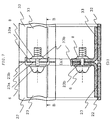
- the case 2 is provided with a concave portion 2d to store the nut 7.
- a major portion of the case 2 relevant to the invention alone is shown for ease of description, and other wiring conductors and structure bodies are omitted.
- the case 2 in which is embedded the wiring conductor 3 is shown by dividing the case 2 to the resin 2a in an upper part and the resin 2b in a lower part for ease of description.
- the case 2 is actually formed in such a manner that the resins 2a and 2b wrap the wiring conductor 3 by insert-molding and the resins 2a and 2b are indistinguishable.
- the wiring terminal surface 3a of the wiring conductor 3 is stored in the concave portion 2c of the case 2 with a clearance in between.
- the wiring terminal surface 3a may be of a structure by which the wiring terminal surface 3a is fixed by insert-molding using resin except for a portion bonded to the wiring terminal surface 4a of the outside wiring terminal 4.
- the concave portion 2d provided to the case 2 so as to store the nut 7 therein has a clearance large enough to insert and move the nut 7.
- it is sufficient that the hook-like protrusion 3b can press the nut 7 softly so that the nut 7 does not come out of the concave portion 2d and strength is not required.
- notch portions 3k are provided to the edge of the wiring terminal surface 3a at the bottom where the hook-like protrusion 3b is formed. Owing to this configuration, there can be achieved an advantage that not only is the hook-like protrusion 3b bent easily, but also the occurrence of strain in the wiring terminal surface 3a and the hook-like protrusion 3b is prevented during the processing.
- this embodiment is particularly effective when applied to a wiring conductor in a power-supply system, which is thick because of a need to flow a large current.
- connection structure of the wiring conductor of the first embodiment for the connection between the wiring terminal of the wiring conductor and the outside wiring terminal to which the flexible wiring is press-fit, by providing the hook-like protrusion to the edge of the wiring terminal surface of the wiring conductor and by pressing and locking the nut, which is the fastening member, with the hook-like protrusion, the need for positioning accuracy of the nut can be eliminated when the bolt is inserted and screwed into the nut. A fastening and bonding work therefore becomes easier. Hence, there can be achieved a significant advantage that work efficiency is enhanced and component costs and operational costs can be reduced.
- Fig. 6 is a schematic perspective view showing a major portion of a connection structure of a wiring conductor of a second embodiment.
- Fig. 7 is a top view with a cross section taken along the line B-B of the connection structure of the wiring conductor.
- a difference from the connection structure of the wiring conductor of the first embodiment above is that in contrast to the first embodiment above in which one wiring terminal is a wiring terminal provided to the case or the wiring conductor on the wiring board and the other wiring terminal is a wiring terminal of the outside wiring terminal to which the flexible wiring is connected and these wiring terminals are interconnected, wiring terminals provided to wiring conductors on two wiring boards are interconnected in the second embodiment.
- a connection structure 40 of a wiring conductor has wiring terminal surfaces 43a and 53a formed in a convex shape by bending to be parallel to wiring conductors 43 and 53, respectively.
- the wiring terminal surface 43a of the wiring conductor 43 on the wiring board 42 and the wiring terminal surface 53a of the wiring conductor 53 on the wiring board 52 are connected.
- Two hook-like protrusions 43b are provided to an edge of the wiring terminal surface 43a and the nut 7 is pressed softly by one hook-like protrusion 43b.
- the wiring terminal surface 53a is pressed and locked as the other hook-like protrusion 43b and the edge of the wiring terminal surface 53a come into contact with each other.
- the wiring terminal surface 53a is thus substantially positioned and fixed. Then, by fastening the bolt 6 with nut 7 by screwing the former into the latter, the wiring conductor 43 on the wiring board 42 and the wiring conductor 53 on the wiring board 52 are electrically connected.
- connection structure of the wiring conductor of the second embodiment is for a case where wiring conductors provided to the case of the electronic device or on the wiring boards are interconnected, and by providing the hook-like protrusions to the edge of the wiring terminal surface of the wiring conductor, and by pressing and locking the other wiring terminal surface by the hook-like protrusions, the bolt is screwed into the nut, both of which are a fastening member.
- positional accuracy of the wiring terminal surfaces with respect to each other is not required, and a fastening and bonding work becomes easier. Accordingly, there can be achieved a significant advantage that work efficiency is enhanced and component costs and operational costs can be reduced.
Description
- The present invention relates to a connection structure of a wiring conductor that electrically interconnects a plurality of wiring terminals of an electronic device.
- In a case where one wiring terminal and the other wiring terminal of an electronic device are connected, a structure typically used in the related art is to firmly fix the terminals by sandwiching the both terminals using a male screw (for example, a bolt) and a female screw (for example, a nut) so that the terminals are electrically and mechanically connected in a reliable manner. In such a structure, however, it is crucial to hold the female screw in a reliable manner when the male screw is fastened and the terminals cannot be connected satisfactorily unless the female screw is stopped from rotating and further the female screw is positioned accurately. Workability is therefore poor.
- To overcome this problem,
PTL 1 describes a power-supply supply terminal, an electronic component with a conductor member, and a structure body including the power-supply supply terminal. The power-supply supply terminal 2 is formed of afirst terminal block 4 and asecond terminal block 20. The firstterminal block 4 is provided with a plurality ofslits 6 to insert press-fit terminals 12 bent in the shape of a capital U and an insert-moldedfemale screw 8. Also, a back wiring board (BWB) 44 has a conductor pattern for a supply of the power supply and a plurality of through-holes connected to the conductor pattern. The power-supply supply terminal 2 is installed to the BWB 44 by inserting press-fit pins 14 of the press-fit terminals 12 into the through-holes of the BWB 44. An outside wiring can be firmly fixed to thefirst terminal block 4 by screwing a male screw 16 into thefemale screw 8 with a press-fit terminal 18 attached to the tip end of the outside wiring sandwiched in between. - PTL 1:
JP-A-2009-43730 - Document
US 5,997,341, December 07, 1999 relates to a terminal connecting-fixing construction for fixedly fastening at least two plate-like terminals to a mating connection portion having connection bolts corresponding respectively to the terminals. - Document
FR 1226070 A, July 08, 1960 -
Document EP 1 355 368 A2, October 22, 2003 relates to a terminal with a nut-positioning device. - With the structure body in the related art including the power-supply supply terminal, positioning accuracy is required for the insert-molded female screw. Hence, there is a problem that component dimensional accuracy and attachment accuracy need to be enhanced. Further, although the female screw itself is fixed in a reliable manner, workability has a problem. The structure body in the related art therefore has another problem that operational costs are increased as working hours become longer.
- The invention was devised to solve the problems discussed above, and has an object to provide a connection structure of a wiring conductor with which working hours can be shorter by making a positioning work easier when a plurality of wiring terminals are electrically interconnected.
- This problem is solved by the independent claims. Advantageous embodiments are described in the dependent claims.
- A connection structure of a wiring conductor of the invention is a connection structure of a wiring conductor that electrically interconnects bonding surfaces of wiring terminals of a plurality of wiring conductors using a fastening member, which is characterized in that at least one wiring terminal is provided with a hook-like protrusion in an edge of the bonding surface, and that the other wiring terminal or the fastening member is pressed and locked by the hook-like protrusion.
- According to the connection structure of the wiring conductor of the invention, by providing the hook-like protrusion to the edge of the bonding surface of at least one wiring terminal, a positioning mechanism can be simpler when the wiring terminals are interconnected. Hence, not only can assembling workability be enhanced, but also dimensional accuracy is not required for the wiring terminals. It thus becomes possible to provide the connection structure at lower costs.
-
- [
Fig. 1] Fig. 1 is a schematic perspective view showing a major portion of a connection structure of a wiring conductor according to a first embodiment of the invention. - [
Fig. 2] Fig. 2 is an exploded perspective view of the connection structure of the wiring conductor ofFig. 1 . - [
Fig. 3] Fig. 3 is a top view with a cross section taken on the line A-A of the connection structure of the wiring conductor ofFig. 1 . - [
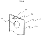
Fig. 4] Fig. 4 is a partial view of a bonding surface portion of a wiring terminal ofFig. 1 . - [
Fig. 5] Fig. 5 is a schematic perspective view showing a major portion of another example of the connection structure of the wiring conductor according to the first embodiment of the invention. - [
Fig. 6] Fig. 6 is a schematic perspective view showing a major portion of a connection structure of a wiring conductor according to a second embodiment of the invention. - [
Fig. 7] Fig. 7 is a top view with a cross section taken on the line B-B of the connection structure of the wiring conductor ofFig. 6 . - [
Fig. 8] Fig. 8 is a schematic perspective view showing a major portion of another example of the connection structure of the wiring conductor according to the second embodiment of the invention. - Hereinafter, a connection structure of a wiring conductor according to embodiments of the invention will be described with reference to
Fig. 1 through Fig. 8 . -
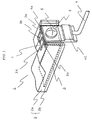
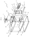
Fig. 1 is a schematic perspective view showing a major portion of a connection structure of a wiring conductor of a first embodiment.Fig. 2 is an exploded perspective view of the connection structure of the wiring conductor.Fig. 3 is a top view with a cross section taken on the line A-A of the connection structure of the wiring conductor. Also,Fig. 4 is a partial view of a bonding surface portion of a wiring terminal. - As are shown in
Fig. 1 andFig. 2 , aconnection structure 1 of a wiring conductor of the first embodiment is formed of acase 2 of an electronic device, a plate-like wiring conductor 3 (hereinafter, referred to as the wiring conductor) insert-molded in thecase 2 usingresins bonding surface 3a of a wiring terminal (hereinafter, referred to as the wiring terminal surface) formed by bending a tip end of thewiring conductor 3, aconcave portion 2c provided to thecase 2 so as to hold and store thewiring terminal surface 3a, a hook-like protrusion 3b provided to an edge of thewiring terminal surface 3a by bending, awiring terminal surface 4a of anoutside wiring terminal 4 oppositely fixed to thewiring terminal surface 3a, a press-fit portion 4f that bonds aflexible wiring 5 to theoutside wiring terminal 4, and a bolt (male screw) 6 and a nut (female screw) 7 pressed and locked by the hook-like protrusion 3b, which are a fastening member that bonds thewiring terminal surface 3a and thewiring terminal surface 4a. Also, thecase 2 is provided with aconcave portion 2d to store thenut 7. In the exploded view of theconnection structure 1 of the wiring conductor ofFig. 2 , a major portion of thecase 2 relevant to the invention alone is shown for ease of description, and other wiring conductors and structure bodies are omitted. Also, thecase 2 in which is embedded thewiring conductor 3 is shown by dividing thecase 2 to theresin 2a in an upper part and theresin 2b in a lower part for ease of description. However, thecase 2 is actually formed in such a manner that theresins wiring conductor 3 by insert-molding and theresins - A function and an effect of the connection structure of the wiring conductor of the first embodiment will now be described. As is shown in the schematic perspective view of
Fig. 1 and the exploded perspective view ofFig. 2 , thewiring terminal surface 4a of theoutside wiring terminal 4 to which is bonded theflexible wiring 5 by the press-fit portion 4f is abutted against thewiring terminal surface 3a exposed from thecase 2. Thebolt 6 is inserted through abonding hole 4h of thewiring terminal surface 4a and abonding hole 3h of thewiring terminal surface 3a and screwed into thenut 7 installed in theconcave portion 2d in advance. Thewiring terminal surface 4a and thewiring terminal surface 3a are thus bonded to each other. In this instance, thenut 7 is locked by being softly pressed by the hook-like protrusion 3b of thewiring terminal surface 3a. Accordingly, thenut 7 is substantially positioned and at the same time thenut 7 is prevented from rotating while thebolt 6 is screwed therein. The need to keep pressing thenut 7 during a work of bonding the wiring terminals to each other is therefore eliminated. Also, thewiring conductor 3 and theflexible wiring 5 can be electrically connected with good work efficiency.Fig. 3 shows the top view (A) and the cross section (B) taken on the line A-A when the connection is completed. - In
Fig. 1 through Fig. 3 , thewiring terminal surface 3a of thewiring conductor 3 is stored in theconcave portion 2c of thecase 2 with a clearance in between. However, thewiring terminal surface 3a may be of a structure by which thewiring terminal surface 3a is fixed by insert-molding using resin except for a portion bonded to thewiring terminal surface 4a of theoutside wiring terminal 4. Also, theconcave portion 2d provided to thecase 2 so as to store thenut 7 therein has a clearance large enough to insert and move thenut 7. Also, as has been described above, it is sufficient that the hook-like protrusion 3b can press thenut 7 softly so that thenut 7 does not come out of theconcave portion 2d and strength is not required. Hence, the hook-like protrusion 3b can be narrow and therefore can be processed easily. Further, it is necessary to position thebolt 6 with respect to the screw hole of thenut 7 when thebolt 6 is fastened by inserting thebolt 6 through thebonding hole 4h and thebonding hole 3h and screwing thebolt 6 into the screw hole of thenut 7. Herein, because thenut 7 is not fixed in theconcave portion 2d and in a loose-fit state, thenut 7 can be fine-tuned so that the center thereof falls on a predetermined position when thebolt 6 is inserted. Hence, it becomes easy to insert thebolt 6 into the screw hole of thenut 7 and positional accuracy as to where thenut 7 is installed is not required. - Also, as is shown in
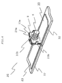
Fig. 4 ,notch portions 3k are provided to the edge of thewiring terminal surface 3a at the bottom where the hook-like protrusion 3b is formed. Owing to this configuration, there can be achieved an advantage that not only is the hook-like protrusion 3b bent easily, but also the occurrence of strain in thewiring terminal surface 3a and the hook-like protrusion 3b is prevented during the processing. - The first embodiment above has described a case where the wiring conductor is embedded in the case. However, a
connection structure 10 of the wiring conductor is also applicable to a case where awiring conductor 13 is provided on awiring board 12 as in another example of the first embodiment shown inFig. 5 . Herein, awiring terminal surface 13a of thewiring conductor 13 processed so as to have an air gap between the self and thewiring board 12 and theoutside wiring terminal 4 are connected. As in the first embodiment above, hook-like protrusions 13b are provided to front and rear edges of thewiring terminal surface 13a (the hook-like protrusion 13b in the rear edge is hidden behind the outside wiring terminal 4), and thenut 7 is pressed softly by these hook-like protrusions 13b. Then, by fastening thebolt 6 with thenut 7 by screwing the former into the latter, thewiring conductor 13 on thewiring board 12 and theoutside wiring terminal 4 are electrically connected. It is sufficient for the wiring conductor to be thick enough to self-stand and bend. Hence, this embodiment is particularly effective when applied to a wiring conductor in a power-supply system, which is thick because of a need to flow a large current. - As has been described, according to the connection structure of the wiring conductor of the first embodiment, for the connection between the wiring terminal of the wiring conductor and the outside wiring terminal to which the flexible wiring is press-fit, by providing the hook-like protrusion to the edge of the wiring terminal surface of the wiring conductor and by pressing and locking the nut, which is the fastening member, with the hook-like protrusion, the need for positioning accuracy of the nut can be eliminated when the bolt is inserted and screwed into the nut. A fastening and bonding work therefore becomes easier. Hence, there can be achieved a significant advantage that work efficiency is enhanced and component costs and operational costs can be reduced.
-
Fig. 6 is a schematic perspective view showing a major portion of a connection structure of a wiring conductor of a second embodiment.Fig. 7 is a top view with a cross section taken along the line B-B of the connection structure of the wiring conductor. A difference from the connection structure of the wiring conductor of the first embodiment above is that in contrast to the first embodiment above in which one wiring terminal is a wiring terminal provided to the case or the wiring conductor on the wiring board and the other wiring terminal is a wiring terminal of the outside wiring terminal to which the flexible wiring is connected and these wiring terminals are interconnected, wiring terminals provided to wiring conductors on two wiring boards are interconnected in the second embodiment. - As is shown in
Fig. 6 , in aconnection structure 20 of the wiring conductor of the second embodiment, wiringconductors wiring boards terminal surfaces wiring conductors like protrusions wiring terminal surfaces like protrusions wiring terminal surface 23a and thewiring terminal surface 33a are abutted against and bonded to each other, thewiring terminal surface 23a and thewiring terminal surface 33a are pressed and locked and therefore substantially positioned. Normally, when thewiring terminal surface 23a and thewiring terminal surface 33a are bonded, it is difficult to position the one with respect to the other unless a specific tool is used. However, by providing the hook-like protrusions 23b to a plurality of points in the edges of thewiring terminal surfaces 23a and suppressing movements of the other wiring terminal surface using the hook-like protrusions 23b, positioning can be performed easily. Then, thebolt 6 is inserted into the bonding hole (hidden in the drawing) of thewiring terminal surface 23a and screwed into thefemale screw 8 provided to thewiring terminal surface 33a by burring. Thewiring terminal surface 23a and thewiring terminal surface 33a are thus bonded. Accordingly, as in the first embodiment above, it becomes possible to interconnect the wiring conductors provided on the wiring boards. The above described a case where the hook-like protrusions wiring terminal surfaces - As has been described, it becomes possible to suppress all movements of the both wiring terminal surfaces to be connected by a plurality of the hook-like protrusions. Hence, because there is no need to use tools and to perform positioning with a high degree of accuracy, the assembling workability can be enhanced.
- The second embodiment has described a case where the wiring conductors are provided on the wiring boards. However, according to another example of the second embodiment shown in
Fig. 8 , aconnection structure 40 of a wiring conductor has wiringterminal surfaces conductors wiring terminal surface 43a of thewiring conductor 43 on thewiring board 42 and thewiring terminal surface 53a of thewiring conductor 53 on thewiring board 52 are connected. Two hook-like protrusions 43b are provided to an edge of thewiring terminal surface 43a and thenut 7 is pressed softly by one hook-like protrusion 43b. Also, thewiring terminal surface 53a is pressed and locked as the other hook-like protrusion 43b and the edge of thewiring terminal surface 53a come into contact with each other. Thewiring terminal surface 53a is thus substantially positioned and fixed. Then, by fastening thebolt 6 withnut 7 by screwing the former into the latter, thewiring conductor 43 on thewiring board 42 and thewiring conductor 53 on thewiring board 52 are electrically connected. - The above has described a case with reference to
Fig. 8 where thewiring terminal surfaces wiring conductors - The female screw used in the second embodiment can be a nut as in the first embodiment above or, a method of directly applying screw-cutting to the wiring terminal surface by burring as has been described above and a method of embedding a helical-insert screw can be used as well.
- As has been described, the connection structure of the wiring conductor of the second embodiment is for a case where wiring conductors provided to the case of the electronic device or on the wiring boards are interconnected, and by providing the hook-like protrusions to the edge of the wiring terminal surface of the wiring conductor, and by pressing and locking the other wiring terminal surface by the hook-like protrusions, the bolt is screwed into the nut, both of which are a fastening member. Hence, positional accuracy of the wiring terminal surfaces with respect to each other is not required, and a fastening and bonding work becomes easier. Accordingly, there can be achieved a significant advantage that work efficiency is enhanced and component costs and operational costs can be reduced.
- The embodiments above have described cases where the wiring terminal surfaces are bonded and electrically connected to each other by screwing the bolt into the nut. However, the invention is not limited to the case of fastening the wiring terminal surfaces by screwing. For example, in a case where the wiring terminal surfaces are bonded by welding, the invention can be also used to temporarily fix the wiring terminal surfaces until welding is applied. Further, even in a case where the wiring terminal surfaces are connected using another component, such as a clip, the invention can be used to temporarily fix the wiring terminal surfaces as well. Furthermore, by forming the tip end of the hook-like protrusion into a fork shape divided to a plurality of branches, the hook-like protrusions can abut against the edge of the other wiring terminal surface at more points and can thereby fix the wiring terminal surface firmly.
- In the respective drawings, the same reference numerals denote same or equivalent portions.
-
- 1, 10, 20, and 40: connection structure of wiring conductor
- 2: case
- 3, 13, 23, 33, 43, and 53: wiring conductor
- 3a, 13a, 23a, 33a, 43a, and 53a: wiring terminal surface
- 3b, 13b, 23b, 33b, 43b: hook-like protrusion
- 3k: notch portion
- 4: outside wiring terminal
- 4a: wiring terminal surface
- 5: flexible wiring
- 6: bolt
- 7: nut
- 8: female screw provided by burring
- 12, 22, 32, 42, and 52: wiring board
Claims (5)
- A connection structure of a wiring conductor that electrically interconnects bonding surfaces (3a, 4a) of wiring terminals of two wiring conductors (3, 4) using a fastening member that includes a bolt (6) and a nut (7), characterized in that:at least one wiring terminal (3) is provided with a hook-like protrusion (3b) in an edge of the bonding surface (3a, 4a); andthe nut is pressed and locked by the hook-like protrusion (3b),wherein the bonding surfaces of the wiring terminals of the two wiring conductors comprise a bonding hole for inserting the bolt.
- The connection structure of the wiring conductor according to claim 1, characterized in that:at least the one wiring conductor (3) is insert-molded with a case (2) of an electronic device.
- The connection structure of the wiring conductor according to claim 1, characterized in that:at least the one wiring conductor (13) is provided on a wiring board (12).
- The connection structure of the wiring conductor according to any one of claim 1 through claim 3, characterized in that:the hook-like protrusion (3b) is formed of the edge of the bonding surface (3a) of the wiring terminal (3) by bending.
- The connection structure of the wiring conductor according to claim 4, characterized in that:a notch portion (3k) is provided to the edge of the bonding surface (3a) of the wiring terminal (3) next to the hook-like protrusion (3b).
Applications Claiming Priority (1)
| Application Number | Priority Date | Filing Date | Title |
|---|---|---|---|
| PCT/JP2011/073380 WO2013054400A1 (en) | 2011-10-12 | 2011-10-12 | Structure for connecting wiring conductor |
Publications (3)
| Publication Number | Publication Date |
|---|---|
| EP2768081A1 EP2768081A1 (en) | 2014-08-20 |
| EP2768081A4 EP2768081A4 (en) | 2015-06-24 |
| EP2768081B1 true EP2768081B1 (en) | 2016-11-30 |
Family
ID=48081479
Family Applications (1)
| Application Number | Title | Priority Date | Filing Date |
|---|---|---|---|
| EP11874076.0A Active EP2768081B1 (en) | 2011-10-12 | 2011-10-12 | Structure for connecting wiring conductor |
Country Status (5)
| Country | Link |
|---|---|
| EP (1) | EP2768081B1 (en) |
| JP (1) | JP5680213B2 (en) |
| CN (1) | CN103858280B (en) |
| IN (1) | IN2014CN03182A (en) |
| WO (1) | WO2013054400A1 (en) |
Families Citing this family (3)
| Publication number | Priority date | Publication date | Assignee | Title |
|---|---|---|---|---|
| JP5847131B2 (en) * | 2013-07-09 | 2016-01-20 | 古河電気工業株式会社 | connector |
| DE102016110050B4 (en) * | 2016-05-31 | 2020-01-23 | Endress+Hauser SE+Co. KG | Plug connection for electrical contacting of a printed circuit board |
| JP7262253B2 (en) * | 2019-03-13 | 2023-04-21 | 日本精機株式会社 | ELECTRONIC COMPONENT MODULE, MOUNTING STRUCTURE FOR ELECTRONIC COMPONENT MODULE AND CASE, AND CONTROL DEVICE INCLUDING THE SAME |
Family Cites Families (7)
| Publication number | Priority date | Publication date | Assignee | Title |
|---|---|---|---|---|
| US1798812A (en) * | 1928-10-06 | 1931-03-31 | J H Rosenbeck & Sons | Electric terminal |
| US2398433A (en) * | 1944-03-18 | 1946-04-16 | Aircraft Marine Prod Inc | Electrical connector |
| FR1226070A (en) * | 1959-05-27 | 1960-07-08 | Low voltage socket and associated switch | |
| JP3371359B2 (en) * | 1997-07-10 | 2003-01-27 | 矢崎総業株式会社 | Terminal connection fixing structure |
| CN2543223Y (en) * | 2002-04-08 | 2003-04-02 | 台湾神户电池股份有限公司 | Terminal with nut locator |
| JP2009043730A (en) | 2003-02-07 | 2009-02-26 | Fujitsu Ltd | Power source feed terminal, electronic part with conductor member, and structure equipped with the power source feed terminal |
| JP2010027410A (en) * | 2008-07-21 | 2010-02-04 | Shang Tsai Wu | Structure of terminal stand |
-
2011
- 2011-10-12 IN IN3182CHN2014 patent/IN2014CN03182A/en unknown
- 2011-10-12 EP EP11874076.0A patent/EP2768081B1/en active Active
- 2011-10-12 JP JP2013538358A patent/JP5680213B2/en active Active
- 2011-10-12 WO PCT/JP2011/073380 patent/WO2013054400A1/en active Application Filing
- 2011-10-12 CN CN201180074096.0A patent/CN103858280B/en active Active
Non-Patent Citations (1)
| Title |
|---|
| None * |
Also Published As
| Publication number | Publication date |
|---|---|
| EP2768081A4 (en) | 2015-06-24 |
| WO2013054400A1 (en) | 2013-04-18 |
| CN103858280B (en) | 2019-04-23 |
| EP2768081A1 (en) | 2014-08-20 |
| JP5680213B2 (en) | 2015-03-04 |
| CN103858280A (en) | 2014-06-11 |
| JPWO2013054400A1 (en) | 2015-03-30 |
| IN2014CN03182A (en) | 2015-07-03 |
Similar Documents
| Publication | Publication Date | Title |
|---|---|---|
| CN101615728B (en) | Beam clamp | |
| US9391385B2 (en) | Dual compressive connector | |
| EP0680113B1 (en) | Electrical connector for conductive leads | |
| US8269116B2 (en) | Circuit board case with electric connector and electronic unit provided with the same | |
| EP1701415A2 (en) | Electronic part-incorporating connector and wiring harness with electronic part-incorporating connector | |
| CN103107429B (en) | Clamping element | |
| CN204167536U (en) | Conductor connecting structure and use the electronic equipment of this syndeton | |
| US8550854B2 (en) | Edge connector | |
| EP2871721B1 (en) | Connecting structure for terminal fitting and substrate | |
| EP2768081B1 (en) | Structure for connecting wiring conductor | |
| CN109075308B (en) | Connection module | |
| WO2018193347A1 (en) | Connector device with connector and assembly method | |
| EP2852264B1 (en) | Electronics module with a side entry connection | |
| EP2622695B1 (en) | A connector for making an electrical connection between two plates | |
| US20110094792A1 (en) | Electrical junction box | |
| JP4774062B2 (en) | Copper bar mounting structure | |
| JP2018182494A (en) | Antenna mounting device and mounting method for antenna device | |
| US20090117760A1 (en) | Terminal connecting structure | |
| US11005197B2 (en) | Control unit having press-fit structure | |
| JP7092729B2 (en) | Terminal and assembly structure of terminal and mounted surface | |
| EP4235975A1 (en) | Plug, connector, and receptacle | |
| JP2024024342A (en) | Earth terminal, terminal mounting structure | |
| JP2006148011A (en) | Fitting structure for electric element to substrate | |
| CN114188903A (en) | Electrical junction box | |
| CN115954697A (en) | Connector with a locking member |
Legal Events
| Date | Code | Title | Description |
|---|---|---|---|
| PUAI | Public reference made under article 153(3) epc to a published international application that has entered the european phase |
Free format text: ORIGINAL CODE: 0009012 |
|
| 17P | Request for examination filed |
Effective date: 20140227 |
|
| AK | Designated contracting states |
Kind code of ref document: A1 Designated state(s): AL AT BE BG CH CY CZ DE DK EE ES FI FR GB GR HR HU IE IS IT LI LT LU LV MC MK MT NL NO PL PT RO RS SE SI SK SM TR |
|
| DAX | Request for extension of the european patent (deleted) | ||
| REG | Reference to a national code |
Ref country code: DE Ref legal event code: R079 Ref document number: 602011033038 Country of ref document: DE Free format text: PREVIOUS MAIN CLASS: H01R0009220000 Ipc: H01R0004300000 |
|
| RA4 | Supplementary search report drawn up and despatched (corrected) |
Effective date: 20150527 |
|
| RIC1 | Information provided on ipc code assigned before grant |
Ipc: H01R 11/26 20060101ALN20150520BHEP Ipc: H01R 4/30 20060101AFI20150520BHEP Ipc: H01R 12/53 20110101ALN20150520BHEP Ipc: H01R 4/34 20060101ALN20150520BHEP |
|
| GRAP | Despatch of communication of intention to grant a patent |
Free format text: ORIGINAL CODE: EPIDOSNIGR1 |
|
| INTG | Intention to grant announced |
Effective date: 20160622 |
|
| GRAS | Grant fee paid |
Free format text: ORIGINAL CODE: EPIDOSNIGR3 |
|
| GRAA | (expected) grant |
Free format text: ORIGINAL CODE: 0009210 |
|
| AK | Designated contracting states |
Kind code of ref document: B1 Designated state(s): AL AT BE BG CH CY CZ DE DK EE ES FI FR GB GR HR HU IE IS IT LI LT LU LV MC MK MT NL NO PL PT RO RS SE SI SK SM TR |
|
| REG | Reference to a national code |
Ref country code: CH Ref legal event code: EP Ref country code: GB Ref legal event code: FG4D |
|
| REG | Reference to a national code |
Ref country code: AT Ref legal event code: REF Ref document number: 850602 Country of ref document: AT Kind code of ref document: T Effective date: 20161215 |
|
| REG | Reference to a national code |
Ref country code: IE Ref legal event code: FG4D |
|
| REG | Reference to a national code |
Ref country code: DE Ref legal event code: R096 Ref document number: 602011033038 Country of ref document: DE |
|
| PG25 | Lapsed in a contracting state [announced via postgrant information from national office to epo] |
Ref country code: LV Free format text: LAPSE BECAUSE OF FAILURE TO SUBMIT A TRANSLATION OF THE DESCRIPTION OR TO PAY THE FEE WITHIN THE PRESCRIBED TIME-LIMIT Effective date: 20161130 |
|
| REG | Reference to a national code |
Ref country code: LT Ref legal event code: MG4D |
|
| REG | Reference to a national code |
Ref country code: NL Ref legal event code: MP Effective date: 20161130 |
|
| REG | Reference to a national code |
Ref country code: AT Ref legal event code: MK05 Ref document number: 850602 Country of ref document: AT Kind code of ref document: T Effective date: 20161130 |
|
| PG25 | Lapsed in a contracting state [announced via postgrant information from national office to epo] |
Ref country code: LT Free format text: LAPSE BECAUSE OF FAILURE TO SUBMIT A TRANSLATION OF THE DESCRIPTION OR TO PAY THE FEE WITHIN THE PRESCRIBED TIME-LIMIT Effective date: 20161130 Ref country code: SE Free format text: LAPSE BECAUSE OF FAILURE TO SUBMIT A TRANSLATION OF THE DESCRIPTION OR TO PAY THE FEE WITHIN THE PRESCRIBED TIME-LIMIT Effective date: 20161130 Ref country code: GR Free format text: LAPSE BECAUSE OF FAILURE TO SUBMIT A TRANSLATION OF THE DESCRIPTION OR TO PAY THE FEE WITHIN THE PRESCRIBED TIME-LIMIT Effective date: 20170301 Ref country code: NO Free format text: LAPSE BECAUSE OF FAILURE TO SUBMIT A TRANSLATION OF THE DESCRIPTION OR TO PAY THE FEE WITHIN THE PRESCRIBED TIME-LIMIT Effective date: 20170228 |
|
| PG25 | Lapsed in a contracting state [announced via postgrant information from national office to epo] |
Ref country code: ES Free format text: LAPSE BECAUSE OF FAILURE TO SUBMIT A TRANSLATION OF THE DESCRIPTION OR TO PAY THE FEE WITHIN THE PRESCRIBED TIME-LIMIT Effective date: 20161130 Ref country code: FI Free format text: LAPSE BECAUSE OF FAILURE TO SUBMIT A TRANSLATION OF THE DESCRIPTION OR TO PAY THE FEE WITHIN THE PRESCRIBED TIME-LIMIT Effective date: 20161130 Ref country code: RS Free format text: LAPSE BECAUSE OF FAILURE TO SUBMIT A TRANSLATION OF THE DESCRIPTION OR TO PAY THE FEE WITHIN THE PRESCRIBED TIME-LIMIT Effective date: 20161130 Ref country code: HR Free format text: LAPSE BECAUSE OF FAILURE TO SUBMIT A TRANSLATION OF THE DESCRIPTION OR TO PAY THE FEE WITHIN THE PRESCRIBED TIME-LIMIT Effective date: 20161130 Ref country code: PT Free format text: LAPSE BECAUSE OF FAILURE TO SUBMIT A TRANSLATION OF THE DESCRIPTION OR TO PAY THE FEE WITHIN THE PRESCRIBED TIME-LIMIT Effective date: 20170330 Ref country code: AT Free format text: LAPSE BECAUSE OF FAILURE TO SUBMIT A TRANSLATION OF THE DESCRIPTION OR TO PAY THE FEE WITHIN THE PRESCRIBED TIME-LIMIT Effective date: 20161130 Ref country code: PL Free format text: LAPSE BECAUSE OF FAILURE TO SUBMIT A TRANSLATION OF THE DESCRIPTION OR TO PAY THE FEE WITHIN THE PRESCRIBED TIME-LIMIT Effective date: 20161130 |
|
| PG25 | Lapsed in a contracting state [announced via postgrant information from national office to epo] |
Ref country code: NL Free format text: LAPSE BECAUSE OF FAILURE TO SUBMIT A TRANSLATION OF THE DESCRIPTION OR TO PAY THE FEE WITHIN THE PRESCRIBED TIME-LIMIT Effective date: 20161130 |
|
| PG25 | Lapsed in a contracting state [announced via postgrant information from national office to epo] |
Ref country code: EE Free format text: LAPSE BECAUSE OF FAILURE TO SUBMIT A TRANSLATION OF THE DESCRIPTION OR TO PAY THE FEE WITHIN THE PRESCRIBED TIME-LIMIT Effective date: 20161130 Ref country code: DK Free format text: LAPSE BECAUSE OF FAILURE TO SUBMIT A TRANSLATION OF THE DESCRIPTION OR TO PAY THE FEE WITHIN THE PRESCRIBED TIME-LIMIT Effective date: 20161130 Ref country code: CZ Free format text: LAPSE BECAUSE OF FAILURE TO SUBMIT A TRANSLATION OF THE DESCRIPTION OR TO PAY THE FEE WITHIN THE PRESCRIBED TIME-LIMIT Effective date: 20161130 Ref country code: SK Free format text: LAPSE BECAUSE OF FAILURE TO SUBMIT A TRANSLATION OF THE DESCRIPTION OR TO PAY THE FEE WITHIN THE PRESCRIBED TIME-LIMIT Effective date: 20161130 Ref country code: RO Free format text: LAPSE BECAUSE OF FAILURE TO SUBMIT A TRANSLATION OF THE DESCRIPTION OR TO PAY THE FEE WITHIN THE PRESCRIBED TIME-LIMIT Effective date: 20161130 |
|
| PG25 | Lapsed in a contracting state [announced via postgrant information from national office to epo] |
Ref country code: SM Free format text: LAPSE BECAUSE OF FAILURE TO SUBMIT A TRANSLATION OF THE DESCRIPTION OR TO PAY THE FEE WITHIN THE PRESCRIBED TIME-LIMIT Effective date: 20161130 Ref country code: BE Free format text: LAPSE BECAUSE OF FAILURE TO SUBMIT A TRANSLATION OF THE DESCRIPTION OR TO PAY THE FEE WITHIN THE PRESCRIBED TIME-LIMIT Effective date: 20161130 Ref country code: BG Free format text: LAPSE BECAUSE OF FAILURE TO SUBMIT A TRANSLATION OF THE DESCRIPTION OR TO PAY THE FEE WITHIN THE PRESCRIBED TIME-LIMIT Effective date: 20170228 Ref country code: IT Free format text: LAPSE BECAUSE OF FAILURE TO SUBMIT A TRANSLATION OF THE DESCRIPTION OR TO PAY THE FEE WITHIN THE PRESCRIBED TIME-LIMIT Effective date: 20161130 |
|
| REG | Reference to a national code |
Ref country code: DE Ref legal event code: R097 Ref document number: 602011033038 Country of ref document: DE |
|
| REG | Reference to a national code |
Ref country code: FR Ref legal event code: PLFP Year of fee payment: 7 |
|
| PLBE | No opposition filed within time limit |
Free format text: ORIGINAL CODE: 0009261 |
|
| STAA | Information on the status of an ep patent application or granted ep patent |
Free format text: STATUS: NO OPPOSITION FILED WITHIN TIME LIMIT |
|
| 26N | No opposition filed |
Effective date: 20170831 |
|
| PG25 | Lapsed in a contracting state [announced via postgrant information from national office to epo] |
Ref country code: SI Free format text: LAPSE BECAUSE OF FAILURE TO SUBMIT A TRANSLATION OF THE DESCRIPTION OR TO PAY THE FEE WITHIN THE PRESCRIBED TIME-LIMIT Effective date: 20161130 |
|
| PG25 | Lapsed in a contracting state [announced via postgrant information from national office to epo] |
Ref country code: MC Free format text: LAPSE BECAUSE OF FAILURE TO SUBMIT A TRANSLATION OF THE DESCRIPTION OR TO PAY THE FEE WITHIN THE PRESCRIBED TIME-LIMIT Effective date: 20161130 |
|
| REG | Reference to a national code |
Ref country code: CH Ref legal event code: PL |
|
| GBPC | Gb: european patent ceased through non-payment of renewal fee |
Effective date: 20171012 |
|
| REG | Reference to a national code |
Ref country code: IE Ref legal event code: MM4A |
|
| PG25 | Lapsed in a contracting state [announced via postgrant information from national office to epo] |
Ref country code: LU Free format text: LAPSE BECAUSE OF NON-PAYMENT OF DUE FEES Effective date: 20171012 Ref country code: CH Free format text: LAPSE BECAUSE OF NON-PAYMENT OF DUE FEES Effective date: 20171031 Ref country code: LI Free format text: LAPSE BECAUSE OF NON-PAYMENT OF DUE FEES Effective date: 20171031 Ref country code: GB Free format text: LAPSE BECAUSE OF NON-PAYMENT OF DUE FEES Effective date: 20171012 |
|
| REG | Reference to a national code |
Ref country code: FR Ref legal event code: PLFP Year of fee payment: 8 |
|
| PG25 | Lapsed in a contracting state [announced via postgrant information from national office to epo] |
Ref country code: MT Free format text: LAPSE BECAUSE OF NON-PAYMENT OF DUE FEES Effective date: 20171012 |
|
| PG25 | Lapsed in a contracting state [announced via postgrant information from national office to epo] |
Ref country code: IE Free format text: LAPSE BECAUSE OF NON-PAYMENT OF DUE FEES Effective date: 20171012 |
|
| REG | Reference to a national code |
Ref country code: DE Ref legal event code: R084 Ref document number: 602011033038 Country of ref document: DE |
|
| PG25 | Lapsed in a contracting state [announced via postgrant information from national office to epo] |
Ref country code: HU Free format text: LAPSE BECAUSE OF FAILURE TO SUBMIT A TRANSLATION OF THE DESCRIPTION OR TO PAY THE FEE WITHIN THE PRESCRIBED TIME-LIMIT; INVALID AB INITIO Effective date: 20111012 |
|
| PG25 | Lapsed in a contracting state [announced via postgrant information from national office to epo] |
Ref country code: CY Free format text: LAPSE BECAUSE OF NON-PAYMENT OF DUE FEES Effective date: 20161130 |
|
| PG25 | Lapsed in a contracting state [announced via postgrant information from national office to epo] |
Ref country code: MK Free format text: LAPSE BECAUSE OF FAILURE TO SUBMIT A TRANSLATION OF THE DESCRIPTION OR TO PAY THE FEE WITHIN THE PRESCRIBED TIME-LIMIT Effective date: 20161130 |
|
| PG25 | Lapsed in a contracting state [announced via postgrant information from national office to epo] |
Ref country code: TR Free format text: LAPSE BECAUSE OF FAILURE TO SUBMIT A TRANSLATION OF THE DESCRIPTION OR TO PAY THE FEE WITHIN THE PRESCRIBED TIME-LIMIT Effective date: 20161130 |
|
| PG25 | Lapsed in a contracting state [announced via postgrant information from national office to epo] |
Ref country code: AL Free format text: LAPSE BECAUSE OF FAILURE TO SUBMIT A TRANSLATION OF THE DESCRIPTION OR TO PAY THE FEE WITHIN THE PRESCRIBED TIME-LIMIT Effective date: 20161130 Ref country code: IS Free format text: LAPSE BECAUSE OF FAILURE TO SUBMIT A TRANSLATION OF THE DESCRIPTION OR TO PAY THE FEE WITHIN THE PRESCRIBED TIME-LIMIT Effective date: 20170330 |
|
| PGFP | Annual fee paid to national office [announced via postgrant information from national office to epo] |
Ref country code: FR Payment date: 20220908 Year of fee payment: 12 |
|
| PGFP | Annual fee paid to national office [announced via postgrant information from national office to epo] |
Ref country code: DE Payment date: 20220621 Year of fee payment: 12 |
|
| P01 | Opt-out of the competence of the unified patent court (upc) registered |
Effective date: 20230512 |