EP2767839A2 - Root mean square detector and circuit breaker using the same - Google Patents
Root mean square detector and circuit breaker using the same Download PDFInfo
- Publication number
- EP2767839A2 EP2767839A2 EP14153156.6A EP14153156A EP2767839A2 EP 2767839 A2 EP2767839 A2 EP 2767839A2 EP 14153156 A EP14153156 A EP 14153156A EP 2767839 A2 EP2767839 A2 EP 2767839A2
- Authority
- EP
- European Patent Office
- Prior art keywords
- transistor
- current
- source
- voltage
- gate
- Prior art date
- Legal status (The legal status is an assumption and is not a legal conclusion. Google has not performed a legal analysis and makes no representation as to the accuracy of the status listed.)
- Granted
Links
Images


Classifications
-
- G—PHYSICS
- G01—MEASURING; TESTING
- G01R—MEASURING ELECTRIC VARIABLES; MEASURING MAGNETIC VARIABLES
- G01R11/00—Electromechanical arrangements for measuring time integral of electric power or current, e.g. of consumption
- G01R11/56—Special tariff meters
-
- G—PHYSICS
- G01—MEASURING; TESTING
- G01R—MEASURING ELECTRIC VARIABLES; MEASURING MAGNETIC VARIABLES
- G01R19/00—Arrangements for measuring currents or voltages or for indicating presence or sign thereof
- G01R19/02—Measuring effective values, i.e. root-mean-square values
-
- G—PHYSICS
- G01—MEASURING; TESTING
- G01R—MEASURING ELECTRIC VARIABLES; MEASURING MAGNETIC VARIABLES
- G01R11/00—Electromechanical arrangements for measuring time integral of electric power or current, e.g. of consumption
- G01R11/30—Dynamo-electric motor meters
-
- G—PHYSICS
- G01—MEASURING; TESTING
- G01R—MEASURING ELECTRIC VARIABLES; MEASURING MAGNETIC VARIABLES
- G01R21/00—Arrangements for measuring electric power or power factor
- G01R21/06—Arrangements for measuring electric power or power factor by measuring current and voltage
-
- H—ELECTRICITY
- H02—GENERATION; CONVERSION OR DISTRIBUTION OF ELECTRIC POWER
- H02H—EMERGENCY PROTECTIVE CIRCUIT ARRANGEMENTS
- H02H3/00—Emergency protective circuit arrangements for automatic disconnection directly responsive to an undesired change from normal electric working condition with or without subsequent reconnection ; integrated protection
-
- G—PHYSICS
- G01—MEASURING; TESTING
- G01R—MEASURING ELECTRIC VARIABLES; MEASURING MAGNETIC VARIABLES
- G01R19/00—Arrangements for measuring currents or voltages or for indicating presence or sign thereof
- G01R19/02—Measuring effective values, i.e. root-mean-square values
- G01R19/03—Measuring effective values, i.e. root-mean-square values using thermoconverters
-
- G—PHYSICS
- G01—MEASURING; TESTING
- G01R—MEASURING ELECTRIC VARIABLES; MEASURING MAGNETIC VARIABLES
- G01R19/00—Arrangements for measuring currents or voltages or for indicating presence or sign thereof
- G01R19/165—Indicating that current or voltage is either above or below a predetermined value or within or outside a predetermined range of values
- G01R19/16533—Indicating that current or voltage is either above or below a predetermined value or within or outside a predetermined range of values characterised by the application
- G01R19/16538—Indicating that current or voltage is either above or below a predetermined value or within or outside a predetermined range of values characterised by the application in AC or DC supplies
- G01R19/16547—Indicating that current or voltage is either above or below a predetermined value or within or outside a predetermined range of values characterised by the application in AC or DC supplies voltage or current in AC supplies
-
- G—PHYSICS
- G06—COMPUTING OR CALCULATING; COUNTING
- G06G—ANALOGUE COMPUTERS
- G06G7/00—Devices in which the computing operation is performed by varying electric or magnetic quantities
- G06G7/12—Arrangements for performing computing operations, e.g. operational amplifiers specially adapted therefor
- G06G7/20—Arrangements for performing computing operations, e.g. operational amplifiers specially adapted therefor for evaluating powers, roots, polynomes, mean square values or standard deviation
Definitions
- the present disclosure relates to a Root Mean Square(abbreviated as RMS hereinafter) detector and a circuit breaker using the same, and more particularly, to a RMS detector for directly computing a signal detected through an analog circuit to measure its RMS value, and a circuit breaker using the same.
- RMS Root Mean Square
- RMS detectors are applied to technologies for calculating and detecting an electric power or the like in a system for detecting the usage of electricity, gas and water and measuring the electric power of a relay or the like, and technologies for performing a root mean square calculation on a current or voltage in a system having a circuit breaker with unnecessary noise to prevent its malfunction, and the like.
- the RMS detector may include a voltage/current signal detector for detecting a current, a voltage or the like, an analog-digital converter for converting an analog signal to a digital signal, a microcontroller or signal processor for computing and processing the converted digital information and controlling the entire system, and a data collector or memory for storing the collected data.
- Patent Document 1 Korean Patent Registration No. 10-0705548
- An aspect of the present disclosure is to provide a RMS detector for directly computing a signal detected through an analog circuit to measure its RMS value, and a circuit breaker using the same.
- Another aspect of the present disclosure is to provide a RMS detector for directly computing a signal detected by an analog circuit in which the entire system is integrated through a Complementary Metal Oxide Semiconductor (abbreviated as CMOS hereinafter) process to measure its RMS value, and a circuit breaker using the same.
- CMOS Complementary Metal Oxide Semiconductor
- Still another aspect of the present disclosure is to provide a RMS detector for measuring a RMS value applicable to application areas such as a circuit breaker that requires high-speed RMS values or the like, and a circuit breaker using the same.
- Yet still another aspect of the present disclosure is to provide a RMS detector for preventing a circuit breaker from being malfunctioned due to noise even when noise is contained in the detected voltage or current, and a circuit breaker suing the same.
- RMS detector comprising:
- RMS detector including the plurality of voltage/current sensing units, the plurality of square circuit units, the summing circuit unit and the root circuit unit is fabricated as an analog circuit that is integrated through the CMOS process, and a signal detected by the relevant fabricated analog circuit is directly computed to measure a RMS value.
- circuit breaker including:
- Still another aspect of the present disclosure as described above may be accomplished by providing a RMS detector for computing the RMS value, which is configured with an analog circuit including the foregoing plurality of voltage/current sensing units, the plurality of square circuit units, the summing circuit unit and the root circuit unit, not to perform computation and processing processes such as digital signal processing using a microprocessor and process program, thereby applying the RMS detector to application areas such as a circuit breaker that requires high speed RMS values or the like to enhance the breaking speed.
- Yet still another aspect of the present disclosure as described above may be accomplished by preventing a circuit breaker from being malfunctioned since it has a configuration using a RMS detector for performing a root mean square calculation on the detected current or voltage value, and additionally, a circuit breaker according to the present disclosure has a configuration in which an output value of the RMS detector is compared with a preset reference value by a comparator for a resultant output so that the circuit breaker may not output a trip control signal responding to any noise having higher voltage than the preset reference value.
- the square circuit unit comprises:
- the square function unit comprises:
- the root function unit comprises:
- the root circuit unit is configured to compute the RMS value by the following equation based on a voltage output from the summing circuit unit, I c ⁇ K ⁇ V in ⁇ 1 2 + K ⁇ V in ⁇ 2 2 + K ⁇ V in ⁇ 3 2 + ... + K ⁇ V inN 2 wherein the I c is a constant current value supplied from a current supply unit, the K is a trans conductance parameter, the V in1 2 through the V inN 2 are voltages output from the plurality of voltage/current sensing unit.
- a circuit breaker to which the RMS detector is applied comprises: a voltage/current sensing unit configured to detect a voltage or current shaped analog signal for an arbitrary electric load; the RMS detector configured to compute a RMS value based on an output voltage of the voltage/current sensing unit; and a comparator configured to compare the RMS value computed and output from the RMS detector with a preset reference voltage to control a switching operation of the circuit breaker.
- the RMS detector is configured to suppress noise contained in an output voltage of the voltage/current sensing unit.
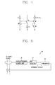
- FIG. 1 is a view illustrating the configuration of a RMS detector 10 according to an embodiment of the present disclosure.
- the RMS detector 10 may include a plurality of voltage/current sensing units 100, a plurality of square circuit units 200, a summing circuit unit 300, and a root circuit unit 400. However, all the constituent elements of the RMS detector 10 as illustrated in FIG. 1 are not necessarily required, and the RMS detector 10 may be implemented with a greater or less number of elements than that of those illustrated elements.
- the voltage/current sensing unit 100 detects a voltage shaped or current shaped analog signal of an arbitrary electric load.
- the arbitrary electric load may be a digital power meter, a digital gas meter, a digital water meter, a digital relay, an electric power meter, and the like.
- the voltage/current sensing unit 100 converts the detected current shaped analog signal into a voltage shaped analog signal.
- the voltage/current sensing unit 100 transfers (in other words outputs) a voltage (for example, V in1 , V in2 , ..., V inN ) detected from the arbitrary electric load to the square circuit unit 200 as illustrated in FIG. 1 .
- the square circuit unit 200 computes a square function based on a voltage output from the voltage/current sensing unit 100.
- the square circuit unit 200 configures a differential circuit based on a differential voltage (V in+ - V in- ) which is an analog signal output from the voltage/current sensing unit 100 to compute the square function.
- the square circuit unit 200 can comprise a square function unit 200b that computes the square function, a root function unit 200c that computes a root function, and a differential circuit 200a for subtracting an output current (I p ) of the root function unit 200c from an output current (I t ) of the square function unit 200b.
- the square function unit 200b may include a first current source I 1 , a second current source I 2 , an output current source I t , and a plurality of transistors (for example, including M 1 and M 2 ).
- the voltages V in+ and the V in- are analog signals output from the voltage/current sensing unit 100.
- one end of the first current source I 1 is connected to a current supplying unit (not shown), and the other end thereof is connected to a source of the first transistor (M 1 ).
- one end of the second current source I 2 is connected to the current supplying unit (not shown), and the other end thereof is connected to a source of the second transistor (M 2 ).
- the source of the first transistor (M 1 ) is connected to the first current source I 1 , and the gate thereof is connected to a voltage output terminal of the voltage/current sensing unit 100 from which output voltage V in+ is output, and the drain thereof is connected to the output current source I t .
- the source of the second transistor (M 2 ) is connected to the second current source I 2 , and the gate thereof is connected to the voltage output terminal of the voltage/current sensing unit 100 from which output voltage V in+ is output, and the drain thereof is connected to the output current source I t .
- One end of the output current source I t is connected to a drain of the first transistor (M 1 ) and a drain of the second transistor (M 2 ), respectively, and the other end thereof is connected to the ground.
- the root function unit may include a first current source I 1 , a second current source I 2 , a third current source I 1 +I 2 +I p , and a plurality of transistors (for example, M 3 , M 4 , M 5 and M 6 ).
- the first current source I 1 and a second current source I 2 in FIG. 4 are not the same as the first current source I 1 and the second current source I 2 in FIG. 3 .
- one end of the first current source I 1 is connected to a current supplying unit (not shown), and the other end thereof is connected to a source of the third transistor (M 3 ), a gate of the fourth transistor (M 4 ) and a gate of the fifth transistor (M 5 ).
- one end of the second current source I 2 is connected to a gate of the third transistor (M 3 ) and a drain of the fourth transistor (M 4 ), and the other end thereof is connected to the ground.
- one end of the third current source I 1 +I 2 +I p is connected to a current supplying unit (not shown), and the other end thereof is connected to a source of the fifth transistor (M 5 ).
- the source of the third transistor (M 3 ) is connected to the first current source I 1 , a gate of the fourth transistor (M 4 ) and a gate of the fifth transistor (M 5 ), and the gate thereof is connected to the second current source I 2 and a drain of the fourth transistor (M 4 ), and the drain thereof is connected to the ground.
- the source of the fourth transistor (M 4 ) is the current supplying unit, and the gate thereof is connected to the first current source I 1 , a source of the third transistor (M 3 ) and a gate of the fifth transistor (M 5 ), and the drain thereof is connected to a gate of the third transistor (M 3 ) and the second current source I 2 .
- the source of the fifth transistor (M 5 ) is the third current source I 1 +I 2 +I p , and the gate thereof is connected to the first current source I 1 , a source of the third transistor (M 3 ) and a gate of the fourth transistor (M 4 ), and the drain thereof is connected to a source and a gate of the sixth transistor (M6).
- the source and gate of the sixth transistor (M6) are connected to a drain of the fifth transistor (M 5 ), and the drain thereof is connected to the ground.
- the output current source I t illustrated in FIG. 3 may be expressed as the following Equation 1 when applying a typical CMOS process among analog circuit design methods.
- the "C ox” is a capacitor value on the gate oxide layer, and the “ ⁇ ” is mobility, and the “W” is a width of the transistor, and the “L” is a length of the transistor.
- Equation 1 is configured with two functions having a square function term and a root function term.
- FIG. 4 is implemented by a root function unit as illustrated in FIG. 4 .
- Equation 4 expressed as I p in FIG. 4
- Equation 1 expressed as I t in FIG. 3
- Equation 5 the square function unit expressed as the following Equation 5 is obtained.
- the square circuit unit 200 has a configuration as illustrated in FIG. 2 , and the output of the square circuit unit 200 has a square function characteristic.
- the summing circuit 300 sums (in other words “adds”) a plurality of output voltages output from the plurality of square circuit units 200, respectively.
- the summing circuit unit 300 sums output voltages in the form of square function units, respectively, output from the plurality of square circuit units 200.
- the summing circuit unit 300 sums output voltages (for example, K ⁇ V in1 2 , K ⁇ V in2 2 , K ⁇ V in3 2 , ... , K ⁇ V inN 2 ) in the form of square functions, respectively, output from the plurality of square circuit units 200 as illustrated in FIG. 1 to output the summed voltage expressed as the following Equation 6.
- the root circuit unit 400 computes a RMS value based on a voltage output from the summing circuit unit 300.
- the root circuit unit 400 computes and outputs the RMS value expressed as the following Equation 7 based on a voltage output from the summing circuit unit 300.
- I c K ⁇ V in ⁇ 1 2 + K ⁇ V in ⁇ 2 2 + K ⁇ V in ⁇ 3 2 + ... + K ⁇ V inN 2
- the RMS detector 10 may be configured with an analog circuit including the plurality of voltage/current sensing units 100, the plurality of square circuit units 200, the summing circuit unit 300 and the root circuit unit 400, and thus directly compute a signal detected through the relevant analog circuit without processes such as digital conversion and computing processing of the central processing unit to measure the RMS value.
- the RMS detector 10 may configure the entire configuration with an analog integrated circuit through a CMOS process, and thus directly compute a signal detected by the relevant analog integrated circuit to measure the RMS value.
- the RMS detector 10 may measure RMS values at high speed by an analog circuit, and thus may be applicable to application areas such as a circuit breaker that requires high-speed RMS values or the like.
- the measurement value calculation function may be implemented through the configuration of such a simple analog circuit, compared to a configuration with high cost elements, such as microprocessor, memory and the like, that requires a long computational processing time.
- FIG. 5 is a block diagram illustrating the configuration of a circuit breaker 20 to which the RMS detector 10 is applied according to an embodiment of the present disclosure.
- the circuit breaker 20 may include a voltage/current sensing unit 21 configured to detect a voltage shaped or current shaped analog signal of an arbitrary electric load, the RMS detector 10 configured to compute a RMS value based on an output voltage of the voltage/current sensing unit 21, and a comparator 22 configured to compare the RMS value computed (or output) from the RMS detector with a preset reference voltage to control the switching operation of the circuit breaker 20.
- circuit breaker 20 illustrated in the drawing, a mechanism for performing a switching operation on an actual circuit, such as a well-known switching mechanism, typically contained in the circuit breaker will be contained in the circuit breaker 20 as a matter of course, but the illustration and description thereof will be omitted since it does not seem to be helpful in the understanding of the features of the present disclosure.
- a root mean square average value processing is primarily carried out by a RMS average signal 620 which is an output value of the RMS detector 10. Furthermore, noise 610 temporarily exceeding the preset reference voltage is secondarily detected by the comparator 22, and thus the resultant output signal 630 of the comparator 22 can be constantly output with no variation regardless of its temporary noise as illustrated in the drawing. Accordingly, a circuit breaker control output signal for controlling a switching mechanism of the circuit breaker to be operated to a circuit opening position may not be generated, thereby surely preventing a malfunction of the circuit breaker 20 being operated to an opening position due to noise.
- a simple analog RMS detector 10 compared to a method of using a peak detector or level detector may be used, thereby allowing a fast detection with no delay due to its computational time.
- a RMS detector may have a configuration in which a signal detected through the analog circuit is directly computed to measure a RMS value as described above, thereby easily and conveniently producing the RMS value.
- the entire configuration of an analog circuit for producing the RMS value may be integrated into a circuit through a CMOS process or the like as described above, thereby minimizing the entire size with low cost.
- a RMS detector has a configuration for producing the RMS value through an analog circuit, and thus a complicated process such as analog-digital conversion, computation and processing with the program and central processing unit or the like may be not carried out, thereby enhancing the circuit breaking speed when applied to application areas such as a circuit breaker that requires high-speed RMS value acquisition or the like.
- a RMS detector and a circuit breaker having the relevant RMS detector may have a configuration for performing a root mean square calculation on a current or voltage in which an output value of the RMS circuit is compared with a reference value by a comparator to output the resultant output value, thereby preventing the reliability of a current or voltage detection value that can be contained in the detected current or voltage signal from being deteriorated as well as the relevant circuit breaker from being malfunctioned.
Landscapes
- Physics & Mathematics (AREA)
- General Physics & Mathematics (AREA)
- Engineering & Computer Science (AREA)
- Power Engineering (AREA)
- Mathematical Physics (AREA)
- Theoretical Computer Science (AREA)
- Software Systems (AREA)
- Computer Hardware Design (AREA)
- Measurement Of Current Or Voltage (AREA)
- Breakers (AREA)
- Gas-Insulated Switchgears (AREA)
Abstract
Description
- The present disclosure relates to a Root Mean Square(abbreviated as RMS hereinafter) detector and a circuit breaker using the same, and more particularly, to a RMS detector for directly computing a signal detected through an analog circuit to measure its RMS value, and a circuit breaker using the same.
- In general, RMS detectors are applied to technologies for calculating and detecting an electric power or the like in a system for detecting the usage of electricity, gas and water and measuring the electric power of a relay or the like, and technologies for performing a root mean square calculation on a current or voltage in a system having a circuit breaker with unnecessary noise to prevent its malfunction, and the like.
- The RMS detector may include a voltage/current signal detector for detecting a current, a voltage or the like, an analog-digital converter for converting an analog signal to a digital signal, a microcontroller or signal processor for computing and processing the converted digital information and controlling the entire system, and a data collector or memory for storing the collected data.
- Patent Document 1: Korean Patent Registration No.
10-0705548 - An aspect of the present disclosure is to provide a RMS detector for directly computing a signal detected through an analog circuit to measure its RMS value, and a circuit breaker using the same.
- Another aspect of the present disclosure is to provide a RMS detector for directly computing a signal detected by an analog circuit in which the entire system is integrated through a Complementary Metal Oxide Semiconductor (abbreviated as CMOS hereinafter) process to measure its RMS value, and a circuit breaker using the same.
- Still another aspect of the present disclosure is to provide a RMS detector for measuring a RMS value applicable to application areas such as a circuit breaker that requires high-speed RMS values or the like, and a circuit breaker using the same.
- Yet still another aspect of the present disclosure is to provide a RMS detector for preventing a circuit breaker from being malfunctioned due to noise even when noise is contained in the detected voltage or current, and a circuit breaker suing the same.
- An aspect of the present disclosure as described above may be accomplished by providing a RMS detector, comprising:
- a plurality of voltage/current sensing units configured to detect a voltage or current shaped analog signal of an arbitrary electric load, and convert the detected current shaped analog signal into a voltage shaped analog signal upon detecting the current shaped analog signal;
- a plurality of square circuit units configured to compute square function, respectively, based on a voltage output from the plurality of voltage/current sensing units;
- a summing circuit unit configured to sum a plurality of output voltages output from the plurality of square circuit units, respectively; and
- a root circuit unit configured to compute a RMS value based on a voltage output from the summing circuit unit.
- Another aspect of the present disclosure as described above may be accomplished by configuring a RMS detector wherein the RMS detector including the plurality of voltage/current sensing units, the plurality of square circuit units, the summing circuit unit and the root circuit unit is fabricated as an analog circuit that is integrated through the CMOS process, and a signal detected by the relevant fabricated analog circuit is directly computed to measure a RMS value.
- Furthermore, another aspect of the present disclosure as described above may be accomplished by providing a circuit breaker, including:
- a voltage/current sensing unit configured to detect a voltage or current shaped analog signal of an arbitrary electric load;
- the RMS detector configured to compute a RMS value based on an output voltage of the voltage/current sensing unit; and
- a comparator configured to compare the RMS value computed from the RMS detector with a preset reference voltage to control the switching operation of the circuit breaker.
- Still another aspect of the present disclosure as described above may be accomplished by providing a RMS detector for computing the RMS value, which is configured with an analog circuit including the foregoing plurality of voltage/current sensing units, the plurality of square circuit units, the summing circuit unit and the root circuit unit, not to perform computation and processing processes such as digital signal processing using a microprocessor and process program, thereby applying the RMS detector to application areas such as a circuit breaker that requires high speed RMS values or the like to enhance the breaking speed.
- Yet still another aspect of the present disclosure as described above may be accomplished by preventing a circuit breaker from being malfunctioned since it has a configuration using a RMS detector for performing a root mean square calculation on the detected current or voltage value, and additionally, a circuit breaker according to the present disclosure has a configuration in which an output value of the RMS detector is compared with a preset reference value by a comparator for a resultant output so that the circuit breaker may not output a trip control signal responding to any noise having higher voltage than the preset reference value.
- According to an aspect of the present disclosure, the square circuit unit comprises:
- a square function unit that computes the square function;
- a root function unit that computes a root function; and
- a differential circuit section configured to subtract an output current of the root function unit from an output current of the square function unit.
- According to another aspect of the present disclosure, the square function unit comprises:
- a first current source having one end of which is connected to a current supply unit, and the other end of which is connected to a source of a first transistor;
- a second current source having one end of which is connected to the current supply unit, and the other end of which is connected to a source of a second transistor;
- the first transistor having a source of which is connected to the first current source, and a gate of which is connected to a voltage output terminal of the voltage/current sensing unit, and a drain of which is connected to an output current source;
- the second transistor having a source of which is connected to the second current source, and a gate of which is connected to the voltage output terminal of the voltage/current sensing unit, and a drain of which is connected to the output current source; and
- the output current source having one end of which is connected to a drain of the first transistor and a drain of the second transistor, respectively, the other end of which is connected to a ground.
- According to still another aspect of the present disclosure, the root function unit comprises:
- a first current source having one end of which is connected to a current supply unit, and the other end of which is connected to a source of a third transistor, a gate of a fourth transistor and a gate of a fifth transistor;
- a second current source having one end of which is connected to a gate of the third transistor and a drain of the fourth transistor, and the other end of which is connected to a ground;
- a third current source having one end of which is connected to the current supply unit, and the other end of which is connected to a source of the fifth transistor;
- the third transistor having a source of which is connected to the first current source, a gate of the fourth transistor and a gate of the fifth transistor, a gate of which is connected to the second current source and a drain of the fourth transistor, and a drain of which is connected to the ground;
- the fourth transistor having a source of which is connected to the current supply unit, a gate of which is connected to the first current source and a source of the third transistor and a gate of the fifth transistor, and a drain of which is connected to a gate of the third transistor and the second current source;
- the fifth transistor having a source of which is connected to the third current source, a gate of which is connected to the first current source, a source of the third transistor and a gate of the fourth transistor, and a drain of which is connected to a source and a gate of a sixth transistor; and
- the six transistor having a source and a gate of which are connected to a drain of the fifth transistor, and a drain of which is connected to the ground.
- According to yet still another aspect of the present disclosure, the root circuit unit is configured to compute the RMS value by the following equation based on a voltage output from the summing circuit unit,

wherein the Ic is a constant current value supplied from a current supply unit, the K is a trans conductance parameter, the Vin1 2 through the VinN 2 are voltages output from the plurality of voltage/current sensing unit. - According to still yet another aspect of the present disclosure, a circuit breaker to which the RMS detector is applied comprises: a voltage/current sensing unit configured to detect a voltage or current shaped analog signal for an arbitrary electric load;
the RMS detector configured to compute a RMS value based on an output voltage of the voltage/current sensing unit; and
a comparator configured to compare the RMS value computed and output from the RMS detector with a preset reference voltage to control a switching operation of the circuit breaker. - According to yet still another aspect of the present disclosure, the RMS detector is configured to suppress noise contained in an output voltage of the voltage/current sensing unit.
- The accompanying drawings, which are included to provide a further understanding of the invention and are incorporated in and constitute a part of this specification, illustrate embodiments of the invention and together with the description serve to explain the principles of the invention.
- In the drawings:
-
FIG. 1 is a view illustrating the configuration of a RMS detector according to an embodiment of the present disclosure; -
FIG. 2 is a block diagram illustrating the configuration of a square circuit unit according to an embodiment of the present disclosure; -
FIG. 3 is a circuit diagram illustrating the configuration of a square function unit contained in the square circuit unit according to an embodiment of the present disclosure; -
FIG. 4 is a circuit diagram illustrating the configuration of a root function unit contained in the square circuit unit according to an embodiment of the present disclosure; -
FIG. 5 is a block diagram illustrating the configuration of a circuit breaker to which the RMS detector is applied according to an embodiment of the present disclosure; and -
FIG. 6 is a waveform diagram a RMS average signal and a comparator output signal which are output values of the RMS detector contained in a circuit breaker according to an embodiment of the present disclosure. - Hereinafter, preferred embodiments of the present invention will be described in detail with reference to the accompanying drawings, and the same or similar elements are designated with the same numeral references regardless of the numerals in the drawings and their redundant description will be omitted.
-
FIG. 1 is a view illustrating the configuration of aRMS detector 10 according to an embodiment of the present disclosure. - As illustrated in
FIG. 1 , theRMS detector 10 may include a plurality of voltage/current sensing units 100, a plurality ofsquare circuit units 200, asumming circuit unit 300, and aroot circuit unit 400. However, all the constituent elements of theRMS detector 10 as illustrated inFIG. 1 are not necessarily required, and theRMS detector 10 may be implemented with a greater or less number of elements than that of those illustrated elements. - The voltage/
current sensing unit 100 detects a voltage shaped or current shaped analog signal of an arbitrary electric load. Here, the arbitrary electric load may be a digital power meter, a digital gas meter, a digital water meter, a digital relay, an electric power meter, and the like. - Furthermore, upon detecting a current shaped analog signal, the voltage/
current sensing unit 100 converts the detected current shaped analog signal into a voltage shaped analog signal. - Furthermore, the voltage/
current sensing unit 100 transfers (in other words outputs) a voltage (for example, Vin1, Vin2, ..., VinN) detected from the arbitrary electric load to thesquare circuit unit 200 as illustrated inFIG. 1 . - The
square circuit unit 200 computes a square function based on a voltage output from the voltage/current sensing unit 100. - In other words, the
square circuit unit 200 configures a differential circuit based on a differential voltage (Vin+ - Vin-) which is an analog signal output from the voltage/current sensing unit 100 to compute the square function. Furthermore, as illustrated inFIG. 2 , thesquare circuit unit 200 can comprise asquare function unit 200b that computes the square function, aroot function unit 200c that computes a root function, and adifferential circuit 200a for subtracting an output current (Ip) of theroot function unit 200c from an output current (It) of thesquare function unit 200b. - Here, the
square function unit 200b may include a first current source I1, a second current source I2, an output current source It, and a plurality of transistors (for example, including M1 and M2). Here, the voltages Vin+ and the Vin- are analog signals output from the voltage/current sensing unit 100. - Here, one end of the first current source I1 is connected to a current supplying unit (not shown), and the other end thereof is connected to a source of the first transistor (M1). Furthermore, one end of the second current source I2 is connected to the current supplying unit (not shown), and the other end thereof is connected to a source of the second transistor (M2). Furthermore, the source of the first transistor (M1) is connected to the first current source I1, and the gate thereof is connected to a voltage output terminal of the voltage/
current sensing unit 100 from which output voltage Vin+ is output, and the drain thereof is connected to the output current source It. - Furthermore, the source of the second transistor (M2) is connected to the second current source I2, and the gate thereof is connected to the voltage output terminal of the voltage/
current sensing unit 100 from which output voltage Vin+ is output, and the drain thereof is connected to the output current source It. - One end of the output current source It is connected to a drain of the first transistor (M1) and a drain of the second transistor (M2), respectively, and the other end thereof is connected to the ground.
- Furthermore, as illustrated in
FIG. 4 , the root function unit may include a first current source I1, a second current source I2, a third current source I1+I2+Ip, and a plurality of transistors (for example, M3, M4, M5 and M6). Here, the first current source I1 and a second current source I2 inFIG. 4 are not the same as the first current source I1 and the second current source I2 inFIG. 3 . - Here, one end of the first current source I1 is connected to a current supplying unit (not shown), and the other end thereof is connected to a source of the third transistor (M3), a gate of the fourth transistor (M4) and a gate of the fifth transistor (M5).
- Furthermore, one end of the second current source I2 is connected to a gate of the third transistor (M3) and a drain of the fourth transistor (M4), and the other end thereof is connected to the ground.
- Furthermore, one end of the third current source I1+I2+Ip is connected to a current supplying unit (not shown), and the other end thereof is connected to a source of the fifth transistor (M5). Furthermore, the source of the third transistor (M3) is connected to the first current source I1, a gate of the fourth transistor (M4) and a gate of the fifth transistor (M5), and the gate thereof is connected to the second current source I2 and a drain of the fourth transistor (M4), and the drain thereof is connected to the ground.
- The source of the fourth transistor (M4) is the current supplying unit, and the gate thereof is connected to the first current source I1, a source of the third transistor (M3) and a gate of the fifth transistor (M5), and the drain thereof is connected to a gate of the third transistor (M3) and the second current source I2. Furthermore, the source of the fifth transistor (M5) is the third current source I1+I2+Ip, and the gate thereof is connected to the first current source I1, a source of the third transistor (M3) and a gate of the fourth transistor (M4), and the drain thereof is connected to a source and a gate of the sixth transistor (M6). Furthermore, the source and gate of the sixth transistor (M6) are connected to a drain of the fifth transistor (M5), and the drain thereof is connected to the ground.
- Furthermore, the output current source It illustrated in
FIG. 3 may be expressed as the followingEquation 1 when applying a typical CMOS process among analog circuit design methods.
- Here, the trans conductance parameter "K" as a process parameter is expressed as follows.

- Here, the "Cox" is a capacitor value on the gate oxide layer, and the "µ" is mobility, and the "W" is a width of the transistor, and the "L" is a length of the transistor.
- Furthermore, the
Equation 1 is configured with two functions having a square function term and a root function term. - Furthermore, the "Ip" illustrated in
FIG. 4 is implemented by a root function unit as illustrated inFIG. 4 . - In other words, when the current I3 flowing through the third transistor (M3) is equal to the current I1, and the current I4 flowing through the fourth transistor (M4) is equal to the current I2, a gate-to-source voltage of the third transistor (M3), fourth transistor (M4), fifth transistor (M5) and sixth transistor (M6) is expressed as the following
Equation 2 based on a loop equation.
- Furthermore, when a basic current equation for CMOS, I = K(Vgs - Vth )2, is applied and a size ratio of the transistor is (W/L)3,4 = 4(W/L)5,6, a relation between the currents I1, I2 and I1+I2+Ip illustrated in
FIG. 4 is expressed as the following Equation 3.
- Hence, the current Ip of the root function unit is expressed as the following Equation 4.

- Hence, for the
square circuit unit 200, when the Equation 4 expressed as Ip inFIG. 4 is subtracted from theEquation 1 expressed as It inFIG. 3 , the square function unit expressed as the following Equation 5 is obtained.
- In this manner, the
square circuit unit 200 has a configuration as illustrated inFIG. 2 , and the output of thesquare circuit unit 200 has a square function characteristic. - The summing circuit (in other words "adder circuit") 300 sums (in other words "adds") a plurality of output voltages output from the plurality of
square circuit units 200, respectively. - In other words, the summing
circuit unit 300 sums output voltages in the form of square function units, respectively, output from the plurality ofsquare circuit units 200. - For an example, the summing
circuit unit 300 sums output voltages (for example, K·Vin1 2, K·Vin2 2, K·Vin3 2, ... , K·VinN 2) in the form of square functions, respectively, output from the plurality ofsquare circuit units 200 as illustrated inFIG. 1 to output the summed voltage expressed as the following Equation 6.
- The root circuit unit (in other words "RMS computing unit") 400 computes a RMS value based on a voltage output from the summing
circuit unit 300. - In other words, when the current from the current sources I1 and I2 illustrated in
FIG. 4 are constant currents Ic, theroot circuit unit 400 computes and outputs the RMS value expressed as the following Equation 7 based on a voltage output from the summingcircuit unit 300.
- As described above, the
RMS detector 10 may be configured with an analog circuit including the plurality of voltage/current sensing units 100, the plurality ofsquare circuit units 200, the summingcircuit unit 300 and theroot circuit unit 400, and thus directly compute a signal detected through the relevant analog circuit without processes such as digital conversion and computing processing of the central processing unit to measure the RMS value. - Furthermore, as described above, the
RMS detector 10 may configure the entire configuration with an analog integrated circuit through a CMOS process, and thus directly compute a signal detected by the relevant analog integrated circuit to measure the RMS value. - Furthermore, as described above, the
RMS detector 10 may measure RMS values at high speed by an analog circuit, and thus may be applicable to application areas such as a circuit breaker that requires high-speed RMS values or the like. - Furthermore, in order to calculate the RMS value, it may be possible to implement the measurement value calculation function through the configuration of such a simple analog circuit, compared to a configuration with high cost elements, such as microprocessor, memory and the like, that requires a long computational processing time.
-
FIG. 5 is a block diagram illustrating the configuration of acircuit breaker 20 to which theRMS detector 10 is applied according to an embodiment of the present disclosure. - As illustrated in
FIG. 5 , thecircuit breaker 20 may include a voltage/current sensing unit 21 configured to detect a voltage shaped or current shaped analog signal of an arbitrary electric load, theRMS detector 10 configured to compute a RMS value based on an output voltage of the voltage/current sensing unit 21, and acomparator 22 configured to compare the RMS value computed (or output) from the RMS detector with a preset reference voltage to control the switching operation of thecircuit breaker 20. - Here, according to the
circuit breaker 20 illustrated in the drawing, a mechanism for performing a switching operation on an actual circuit, such as a well-known switching mechanism, typically contained in the circuit breaker will be contained in thecircuit breaker 20 as a matter of course, but the illustration and description thereof will be omitted since it does not seem to be helpful in the understanding of the features of the present disclosure. - Due to the foregoing configuration, as illustrated in
FIG. 6 , even whennoise 610 is contained in a voltage or current sensing signal detected from the voltage/current sensing unit 21, a root mean square average value processing is primarily carried out by a RMSaverage signal 620 which is an output value of theRMS detector 10. Furthermore,noise 610 temporarily exceeding the preset reference voltage is secondarily detected by thecomparator 22, and thus theresultant output signal 630 of thecomparator 22 can be constantly output with no variation regardless of its temporary noise as illustrated in the drawing. Accordingly, a circuit breaker control output signal for controlling a switching mechanism of the circuit breaker to be operated to a circuit opening position may not be generated, thereby surely preventing a malfunction of thecircuit breaker 20 being operated to an opening position due to noise. - Furthermore, a simple
analog RMS detector 10 compared to a method of using a peak detector or level detector may be used, thereby allowing a fast detection with no delay due to its computational time. - A RMS detector according to an embodiment of the present disclosure may have a configuration in which a signal detected through the analog circuit is directly computed to measure a RMS value as described above, thereby easily and conveniently producing the RMS value.
- Furthermore, in a RMS detector according to an embodiment of the present disclosure, the entire configuration of an analog circuit for producing the RMS value may be integrated into a circuit through a CMOS process or the like as described above, thereby minimizing the entire size with low cost.
- Furthermore, a RMS detector according to an embodiment of the present disclosure has a configuration for producing the RMS value through an analog circuit, and thus a complicated process such as analog-digital conversion, computation and processing with the program and central processing unit or the like may be not carried out, thereby enhancing the circuit breaking speed when applied to application areas such as a circuit breaker that requires high-speed RMS value acquisition or the like.
- Furthermore, a RMS detector and a circuit breaker having the relevant RMS detector according to an embodiment of the present disclosure may have a configuration for performing a root mean square calculation on a current or voltage in which an output value of the RMS circuit is compared with a reference value by a comparator to output the resultant output value, thereby preventing the reliability of a current or voltage detection value that can be contained in the detected current or voltage signal from being deteriorated as well as the relevant circuit breaker from being malfunctioned.
- It will be apparent to those skilled in this art that various changes and modifications may be made thereto without departing from the gist of the present invention. Accordingly, it should be noted that the embodiments disclosed in the present invention are only illustrative and not limitative to the concept of the present invention, and the scope of the concept of the invention is not limited by those embodiments. The scope protected by the present invention should be construed by the accompanying claims, and all the concept within the equivalent scope of the invention should be construed to be included in the scope of the right of the present invention.
Claims (11)
- A RMS detector, characterized in that the RMS detector comprising:a plurality of voltage/current sensing units (100) configured to detect a voltage or current shaped analog signal of an arbitrary electric load, and convert the detected current shaped analog signal into a voltage shaped analog signal upon detecting the current shaped analog signal;a plurality of square circuit units (200) configured to compute square function, respectively, based on a voltage output from the plurality of voltage/current sensing units (100);a summing circuit unit (300) configured to sum a plurality of output voltages output from the plurality of square circuit units (200), respectively; anda root circuit unit (400) configured to compute a RMS value based on a voltage output from the summing circuit unit (300).
- The RMS detector of claim 1, wherein the square circuit unit (200) comprises:a square function unit (200b) that computes the square function;a root function unit (200c) that computes a root function; anda differential circuit (200a) configured to subtract an output current of the root function unit (200c) from an output current of the square function unit (200b).
- The RMS detector of claim 2, wherein the square function unit (200b) comprises:a first current source (I1) having one end of which is connected to a current supply unit, and the other end of which is connected to a source of a first transistor (M1);a second current source (I2) having one end of which is connected to the current supply unit, and the other end of which is connected to a source of a second transistor (M2);the first transistor (M1) having a source of which is connected to the first current source (I1), and a gate of which is connected to a voltage output terminal of the voltage/current sensing unit (100), and a drain of which is connected to an output current source (It);the second transistor (M2) having a source of which is connected to the second current source (I2), and a gate of which is connected to the voltage output terminal of the voltage/current sensing unit (100), and a drain of which is connected to the output current source (It); andthe output current source (It) having one end of which is connected to a drain of the first transistor (M1) and a drain of the second transistor (M2), respectively, the other end of which is connected to a ground.
- The RMS detector of claim 2, wherein the root function unit (200c) comprises:a first current source (I1) having one end of which is connected to a current supply unit, and the other end of which is connected to a source of a third transistor (M3), a gate of a fourth transistor (M4) and a gate of a fifth transistor (M5);a second current source (I2) having one end of which is connected to a gate of the third transistor (M3) and a drain of the fourth transistor (M4), and the other end of which is connected to a ground;a third current source (I1 + I2 + Ip) having one end of which is connected to the current supply unit, and the other end of which is connected to a source of the fifth transistor (M5);the third transistor (M3) having a source of which is connected to the first current source (I1), a gate of the fourth transistor (M4) and a gate of the fifth transistor (M5), a gate of which is connected to the second current source (I2) and a drain of the fourth transistor (M4), and a drain of which is connected to the ground;the fourth transistor (M4) having a source of which is connected to the current supply unit, a gate of which is connected to the first current source (I1) and a source of the third transistor (M3) and a gate of the fifth transistor (M5), and a drain of which is connected to a gate of the third transistor (M3) and the second current source (I2);the fifth transistor (M5) having a source of which is connected to the third current source (I1 + I2 + Ip), a gate of which is connected to the first current source (I1), a source of the third transistor (M3) and a gate of the fourth transistor (M4), and a drain of which is connected to a source and a gate of a sixth transistor (M6); andthe six transistor (M6) having a source and a gate of which are connected to a drain of the fifth transistor (M5), and a drain of which is connected to the ground.
- The RMS detector of any one of claims 1-4, wherein the root circuit unit (400) is configured to compute the RMS value by the following equation based on a voltage output from the summing circuit unit (300),

wherein the Ic is a constant current value supplied from a current supply unit, the K is a trans conductance parameter, the Vin1 2 through the VinN 2 are voltages output from the plurality of voltage/current sensing unit (100). - A circuit breaker of claim 1, characterized in that the circuit breaker comprising:a voltage/current sensing unit (21) configured to detect a voltage or current shaped analog signal of an arbitrary electric load;a RMS detector (10) configured to compute a RMS value based on an output voltage of the voltage/current sensing unit (21); anda comparator (22) configured to compare the RMS value computed and output from the RMS detector (10) with a preset reference voltage to control a switching operation of the circuit breaker,wherein the RMS detector (10) comprises:a square circuit unit (200) configured to compute a square function based on a voltage output from the voltage/current sensing unit (21);a summing circuit unit (300) configured to sum a voltage output from the square circuit unit (200); anda root circuit unit (400) configured to compute a RMS value based on a voltage output from the summing circuit unit (300).
- The circuit breaker of claim 6, wherein the RMS detector (10) is configured to suppress noise contained in an output voltage of the voltage/current sensing unit (21).
- The circuit breaker of claim 6 or claim 7, wherein the square circuit unit (200) comprises:a square function unit (200b) that computes the square function;a root function unit (200c) that computes a root function; anda differential circuit (200a) configured to subtract an output current of the root function unit (200c) from an output current of the square function unit (200b).
- The circuit breaker of claim 8, wherein the square function unit (200b) comprises:a first current source (I1) having one end of which is connected to a current supply unit, and the other end of which is connected to a source of a first transistor (M1);a second current source (I2) having one end of which is connected to the current supply unit, and the other end of which is connected to a source of a second transistor (M2);the first transistor (M1) having a source of which is connected to the first current source (I1), and a gate of which is connected to a voltage output terminal of the voltage/current sensing unit (21), and a drain of which is connected to an output current source (It);the second transistor (M2) having a source of which is connected to the second current source (I2), and a gate of which is connected to the voltage output terminal of the voltage/current sensing unit (21), and a drain of which is connected to the output current source (It); andthe output current source (It) having one end of which is connected to a drain of the first transistor (M1) and a drain of the second transistor (M2), respectively, the other end of which is connected to a ground.
- The circuit breaker of claim 8, wherein the root function unit (200c) comprises:a first current source (I1) having one end of which is connected to a current supply unit, and the other end of which is connected to a source of a third transistor (M3), a gate of a fourth transistor (M4) and a gate of a fifth transistor (M5);a second current source (I2) having one end of which is connected to a gate of the third transistor (M3) and a drain of the fourth transistor (M4), and the other end of which is connected to a ground;a third current source (I1 + I2 + Ip) having one end of which is connected to the current supply unit, and the other end of which is connected to a source of the fifth transistor (M5);the third transistor (M3) having a source of which is connected to the first current source (I1), a gate of the fourth transistor (M4) and a gate of the fifth transistor (M5), a gate of which is connected to the second current source (I2) and a drain of the fourth transistor (M4), and a drain of which is connected to the ground;the fourth transistor (M4) having a source of which is connected to the current supply unit, a gate of which is connected to the first current source and a source of the third transistor (M3) and a gate of the fifth transistor (M5), and a drain of which is connected to a gate of the third transistor (M3) and the second current source (I2);the fifth transistor (M5) having a source of which is connected to the third current source (I1 + I2 + Ip), a gate of which is connected to the first current source (I1), a source of the third transistor (M3) and a gate of the fourth transistor (M4), and a drain of which is connected to a source and a gate of a sixth transistor (M6); andthe sixth transistor (M6) having a source and a gate of which are connected to a drain of the fifth transistor (M5), and a drain of which is connected to the ground.
- The circuit breaker of any one of claims 6-10, wherein the root circuit unit (400) is configured to compute the RMS value by the following equation based on a voltage output from the summing circuit unit (300),

wherein the Ic is a constant current value supplied from a current supply unit, the K is a trans conductance parameter, the Vin1 2 through the VinN 2 are voltages output from the plurality of voltage/current sensing unit (100).
Applications Claiming Priority (1)
| Application Number | Priority Date | Filing Date | Title |
|---|---|---|---|
| KR1020130017173A KR101774245B1 (en) | 2013-02-18 | 2013-02-18 | Root-mean square detector and circuit breaker thereof |
Publications (3)
| Publication Number | Publication Date |
|---|---|
| EP2767839A2 true EP2767839A2 (en) | 2014-08-20 |
| EP2767839A3 EP2767839A3 (en) | 2017-12-20 |
| EP2767839B1 EP2767839B1 (en) | 2020-04-01 |
Family
ID=50002624
Family Applications (1)
| Application Number | Title | Priority Date | Filing Date |
|---|---|---|---|
| EP14153156.6A Not-in-force EP2767839B1 (en) | 2013-02-18 | 2014-01-30 | Root mean square detector and circuit breaker using the same |
Country Status (6)
| Country | Link |
|---|---|
| US (1) | US9194891B2 (en) |
| EP (1) | EP2767839B1 (en) |
| JP (1) | JP5833691B2 (en) |
| KR (1) | KR101774245B1 (en) |
| CN (1) | CN103995173B (en) |
| ES (1) | ES2799301T3 (en) |
Families Citing this family (4)
| Publication number | Priority date | Publication date | Assignee | Title |
|---|---|---|---|---|
| KR102452352B1 (en) * | 2016-04-18 | 2022-10-07 | 엘에스일렉트릭(주) | Analog signal detecting circuit |
| US10352955B2 (en) | 2016-04-20 | 2019-07-16 | Hamilton Sundstrand Corporation | Rotary speed sensors |
| CN206638735U (en) * | 2017-01-20 | 2017-11-14 | 福迪威(上海)工业仪器技术研发有限公司 | Pincerlike meter |
| US10809284B2 (en) | 2017-10-31 | 2020-10-20 | Microchip Technology Incorporated | Systems and methods for improved root mean square (RMS) measurement |
Family Cites Families (17)
| Publication number | Priority date | Publication date | Assignee | Title |
|---|---|---|---|---|
| JPS60244866A (en) | 1984-05-21 | 1985-12-04 | Nishishiba Denki Kk | Voltage detecting device for three-phase alternating current |
| JPS6324377A (en) | 1986-07-16 | 1988-02-01 | Nec Corp | Squaring circuit |
| JPH06105266B2 (en) * | 1987-12-28 | 1994-12-21 | 三菱電機株式会社 | Digital protection relay |
| JPH0737997B2 (en) * | 1988-10-31 | 1995-04-26 | 三菱電機株式会社 | Electricity detector |
| JPH0737998B2 (en) * | 1988-11-16 | 1995-04-26 | 三菱電機株式会社 | Electricity detector |
| US5065053A (en) | 1990-02-26 | 1991-11-12 | Digital Equipment Corporation Of Canada, Ltd. | Exponential function circuitry |
| JPH05128960A (en) | 1991-11-06 | 1993-05-25 | Mitsubishi Electric Corp | Circuit breaker |
| JP3269220B2 (en) | 1993-04-28 | 2002-03-25 | 株式会社明電舎 | Transformer protection relay |
| JP2848436B2 (en) | 1994-08-12 | 1999-01-20 | 日本電気株式会社 | Square circuit |
| US5644238A (en) * | 1995-06-07 | 1997-07-01 | Seifert; Gregory J. | Method and apparatus for comparing load current in an electrical circuit with the capacity of its supply source |
| JPH10229311A (en) | 1997-02-17 | 1998-08-25 | Nec Corp | Mos line transconductance amplifier |
| JPH11250168A (en) | 1998-03-04 | 1999-09-17 | Nec Corp | Square number calculation circuit, composite deferential amplifier circuit and multiplier using these circuits |
| DE19822127A1 (en) * | 1998-05-07 | 1999-11-11 | Siemens Ag | Method and circuit arrangement for current detection |
| JP4611230B2 (en) | 2006-03-28 | 2011-01-12 | Nttエレクトロニクス株式会社 | Wavelength converter |
| US20100091419A1 (en) * | 2008-10-15 | 2010-04-15 | Vedula Sastry V | Motor drive ground fault detection |
| JP2010114710A (en) | 2008-11-07 | 2010-05-20 | Seiko Epson Corp | Electronic circuit, electronic device equipped with the same, and pulse detection method of electronic device |
| US8823356B2 (en) * | 2011-03-21 | 2014-09-02 | Solarbridge Technologies, Inc. | Supply voltage auto-sensing |
-
2013
- 2013-02-18 KR KR1020130017173A patent/KR101774245B1/en active Active
-
2014
- 2014-01-29 US US14/167,874 patent/US9194891B2/en active Active
- 2014-01-30 EP EP14153156.6A patent/EP2767839B1/en not_active Not-in-force
- 2014-01-30 ES ES14153156T patent/ES2799301T3/en active Active
- 2014-02-18 JP JP2014028466A patent/JP5833691B2/en active Active
- 2014-02-18 CN CN201410054948.5A patent/CN103995173B/en active Active
Non-Patent Citations (1)
| Title |
|---|
| None |
Also Published As
| Publication number | Publication date |
|---|---|
| EP2767839A3 (en) | 2017-12-20 |
| US9194891B2 (en) | 2015-11-24 |
| KR101774245B1 (en) | 2017-09-19 |
| CN103995173A (en) | 2014-08-20 |
| EP2767839B1 (en) | 2020-04-01 |
| ES2799301T3 (en) | 2020-12-16 |
| JP5833691B2 (en) | 2015-12-16 |
| JP2014157155A (en) | 2014-08-28 |
| US20140233144A1 (en) | 2014-08-21 |
| CN103995173B (en) | 2017-04-12 |
| KR20140103599A (en) | 2014-08-27 |
Similar Documents
| Publication | Publication Date | Title |
|---|---|---|
| US7576547B2 (en) | Measuring array | |
| EP2192416B1 (en) | Method and apparatus for detecting a phase-to-earth fault | |
| EP3066481B1 (en) | Systems and methods for insulation impedance monitoring | |
| EP2741094A1 (en) | Ground fault detection device, ground fault detection method, solar energy system, and ground fault detection program | |
| US9768610B2 (en) | Method and circuit arrangement with means for a leakage current compensation in a photovoltaic system with multiple differential current sensors | |
| US9768605B2 (en) | Arc fault detection system and method and circuit interrupter employing same | |
| JP6220209B2 (en) | DC feeding protection control system | |
| EP2767839B1 (en) | Root mean square detector and circuit breaker using the same | |
| KR101952063B1 (en) | Leakage current detection device | |
| US20160187408A1 (en) | Arc fault detection system and method and circuit interrupter employing same | |
| CN109154630B (en) | Overcurrent element in time domain | |
| JP2011015583A (en) | Leakage detection method, leakage detection device, and earth leakage breaker | |
| CN115372684A (en) | Current measurement circuit for a converter, converter circuit and converter | |
| JP2021065073A (en) | Protective relay device | |
| JP5444122B2 (en) | Non-grounded circuit ground fault detection device, ground fault protection relay using the same, and ground fault detection method | |
| US9466969B2 (en) | Master-slave digital circuit breakers | |
| MX2019000605A (en) | Electronic overload breaker with built-in shunt calibration (bisc) and methods of operating same. | |
| KR102006186B1 (en) | Digital protective relay | |
| WO2013066212A3 (en) | Method for determining the distance to a fault on a power transmission line and device for the implementation thereof | |
| CN110120655B (en) | Frequency tracking system and method for rear-end current channel of frequency converter | |
| KR101309400B1 (en) | Merging unit with frequency protection function | |
| CN111521857A (en) | Multi-conductor current measuring system based on TMR tunnel magnetic resistance | |
| JP2012156659A (en) | Current detection circuit | |
| CN108291938B (en) | Monitoring of input signal channels | |
| EP4488696B1 (en) | Fault location detection in tapped power distribution lines |
Legal Events
| Date | Code | Title | Description |
|---|---|---|---|
| PUAI | Public reference made under article 153(3) epc to a published international application that has entered the european phase |
Free format text: ORIGINAL CODE: 0009012 |
|
| 17P | Request for examination filed |
Effective date: 20140130 |
|
| AK | Designated contracting states |
Kind code of ref document: A2 Designated state(s): AL AT BE BG CH CY CZ DE DK EE ES FI FR GB GR HR HU IE IS IT LI LT LU LV MC MK MT NL NO PL PT RO RS SE SI SK SM TR |
|
| AX | Request for extension of the european patent |
Extension state: BA ME |
|
| PUAL | Search report despatched |
Free format text: ORIGINAL CODE: 0009013 |
|
| AK | Designated contracting states |
Kind code of ref document: A3 Designated state(s): AL AT BE BG CH CY CZ DE DK EE ES FI FR GB GR HR HU IE IS IT LI LT LU LV MC MK MT NL NO PL PT RO RS SE SI SK SM TR |
|
| AX | Request for extension of the european patent |
Extension state: BA ME |
|
| RIC1 | Information provided on ipc code assigned before grant |
Ipc: H02H 3/00 20060101ALI20171114BHEP Ipc: G06G 7/20 20060101ALI20171114BHEP Ipc: G01R 19/03 20060101ALI20171114BHEP Ipc: G01R 19/02 20060101AFI20171114BHEP Ipc: G01R 21/06 20060101ALI20171114BHEP Ipc: G01R 19/165 20060101ALI20171114BHEP |
|
| STAA | Information on the status of an ep patent application or granted ep patent |
Free format text: STATUS: REQUEST FOR EXAMINATION WAS MADE |
|
| R17P | Request for examination filed (corrected) |
Effective date: 20180619 |
|
| RBV | Designated contracting states (corrected) |
Designated state(s): AL AT BE BG CH CY CZ DE DK EE ES FI FR GB GR HR HU IE IS IT LI LT LU LV MC MK MT NL NO PL PT RO RS SE SI SK SM TR |
|
| GRAP | Despatch of communication of intention to grant a patent |
Free format text: ORIGINAL CODE: EPIDOSNIGR1 |
|
| STAA | Information on the status of an ep patent application or granted ep patent |
Free format text: STATUS: GRANT OF PATENT IS INTENDED |
|
| INTG | Intention to grant announced |
Effective date: 20191122 |
|
| GRAS | Grant fee paid |
Free format text: ORIGINAL CODE: EPIDOSNIGR3 |
|
| GRAA | (expected) grant |
Free format text: ORIGINAL CODE: 0009210 |
|
| STAA | Information on the status of an ep patent application or granted ep patent |
Free format text: STATUS: THE PATENT HAS BEEN GRANTED |
|
| AK | Designated contracting states |
Kind code of ref document: B1 Designated state(s): AL AT BE BG CH CY CZ DE DK EE ES FI FR GB GR HR HU IE IS IT LI LT LU LV MC MK MT NL NO PL PT RO RS SE SI SK SM TR |
|
| REG | Reference to a national code |
Ref country code: GB Ref legal event code: FG4D |
|
| REG | Reference to a national code |
Ref country code: AT Ref legal event code: REF Ref document number: 1252063 Country of ref document: AT Kind code of ref document: T Effective date: 20200415 Ref country code: CH Ref legal event code: EP |
|
| REG | Reference to a national code |
Ref country code: DE Ref legal event code: R096 Ref document number: 602014063038 Country of ref document: DE |
|
| REG | Reference to a national code |
Ref country code: IE Ref legal event code: FG4D |
|
| PG25 | Lapsed in a contracting state [announced via postgrant information from national office to epo] |
Ref country code: BG Free format text: LAPSE BECAUSE OF FAILURE TO SUBMIT A TRANSLATION OF THE DESCRIPTION OR TO PAY THE FEE WITHIN THE PRESCRIBED TIME-LIMIT Effective date: 20200701 |
|
| REG | Reference to a national code |
Ref country code: NL Ref legal event code: MP Effective date: 20200401 |
|
| REG | Reference to a national code |
Ref country code: LT Ref legal event code: MG4D |
|
| PG25 | Lapsed in a contracting state [announced via postgrant information from national office to epo] |
Ref country code: CZ Free format text: LAPSE BECAUSE OF FAILURE TO SUBMIT A TRANSLATION OF THE DESCRIPTION OR TO PAY THE FEE WITHIN THE PRESCRIBED TIME-LIMIT Effective date: 20200401 Ref country code: GR Free format text: LAPSE BECAUSE OF FAILURE TO SUBMIT A TRANSLATION OF THE DESCRIPTION OR TO PAY THE FEE WITHIN THE PRESCRIBED TIME-LIMIT Effective date: 20200702 Ref country code: NO Free format text: LAPSE BECAUSE OF FAILURE TO SUBMIT A TRANSLATION OF THE DESCRIPTION OR TO PAY THE FEE WITHIN THE PRESCRIBED TIME-LIMIT Effective date: 20200701 Ref country code: IS Free format text: LAPSE BECAUSE OF FAILURE TO SUBMIT A TRANSLATION OF THE DESCRIPTION OR TO PAY THE FEE WITHIN THE PRESCRIBED TIME-LIMIT Effective date: 20200801 Ref country code: SE Free format text: LAPSE BECAUSE OF FAILURE TO SUBMIT A TRANSLATION OF THE DESCRIPTION OR TO PAY THE FEE WITHIN THE PRESCRIBED TIME-LIMIT Effective date: 20200401 Ref country code: LT Free format text: LAPSE BECAUSE OF FAILURE TO SUBMIT A TRANSLATION OF THE DESCRIPTION OR TO PAY THE FEE WITHIN THE PRESCRIBED TIME-LIMIT Effective date: 20200401 Ref country code: FI Free format text: LAPSE BECAUSE OF FAILURE TO SUBMIT A TRANSLATION OF THE DESCRIPTION OR TO PAY THE FEE WITHIN THE PRESCRIBED TIME-LIMIT Effective date: 20200401 Ref country code: NL Free format text: LAPSE BECAUSE OF FAILURE TO SUBMIT A TRANSLATION OF THE DESCRIPTION OR TO PAY THE FEE WITHIN THE PRESCRIBED TIME-LIMIT Effective date: 20200401 Ref country code: PT Free format text: LAPSE BECAUSE OF FAILURE TO SUBMIT A TRANSLATION OF THE DESCRIPTION OR TO PAY THE FEE WITHIN THE PRESCRIBED TIME-LIMIT Effective date: 20200817 |
|
| REG | Reference to a national code |
Ref country code: AT Ref legal event code: MK05 Ref document number: 1252063 Country of ref document: AT Kind code of ref document: T Effective date: 20200401 |
|
| PG25 | Lapsed in a contracting state [announced via postgrant information from national office to epo] |
Ref country code: LV Free format text: LAPSE BECAUSE OF FAILURE TO SUBMIT A TRANSLATION OF THE DESCRIPTION OR TO PAY THE FEE WITHIN THE PRESCRIBED TIME-LIMIT Effective date: 20200401 Ref country code: HR Free format text: LAPSE BECAUSE OF FAILURE TO SUBMIT A TRANSLATION OF THE DESCRIPTION OR TO PAY THE FEE WITHIN THE PRESCRIBED TIME-LIMIT Effective date: 20200401 Ref country code: RS Free format text: LAPSE BECAUSE OF FAILURE TO SUBMIT A TRANSLATION OF THE DESCRIPTION OR TO PAY THE FEE WITHIN THE PRESCRIBED TIME-LIMIT Effective date: 20200401 |
|
| REG | Reference to a national code |
Ref country code: ES Ref legal event code: FG2A Ref document number: 2799301 Country of ref document: ES Kind code of ref document: T3 Effective date: 20201216 |
|
| PG25 | Lapsed in a contracting state [announced via postgrant information from national office to epo] |
Ref country code: AL Free format text: LAPSE BECAUSE OF FAILURE TO SUBMIT A TRANSLATION OF THE DESCRIPTION OR TO PAY THE FEE WITHIN THE PRESCRIBED TIME-LIMIT Effective date: 20200401 |
|
| REG | Reference to a national code |
Ref country code: DE Ref legal event code: R097 Ref document number: 602014063038 Country of ref document: DE |
|
| PG25 | Lapsed in a contracting state [announced via postgrant information from national office to epo] |
Ref country code: AT Free format text: LAPSE BECAUSE OF FAILURE TO SUBMIT A TRANSLATION OF THE DESCRIPTION OR TO PAY THE FEE WITHIN THE PRESCRIBED TIME-LIMIT Effective date: 20200401 Ref country code: RO Free format text: LAPSE BECAUSE OF FAILURE TO SUBMIT A TRANSLATION OF THE DESCRIPTION OR TO PAY THE FEE WITHIN THE PRESCRIBED TIME-LIMIT Effective date: 20200401 Ref country code: DK Free format text: LAPSE BECAUSE OF FAILURE TO SUBMIT A TRANSLATION OF THE DESCRIPTION OR TO PAY THE FEE WITHIN THE PRESCRIBED TIME-LIMIT Effective date: 20200401 Ref country code: SM Free format text: LAPSE BECAUSE OF FAILURE TO SUBMIT A TRANSLATION OF THE DESCRIPTION OR TO PAY THE FEE WITHIN THE PRESCRIBED TIME-LIMIT Effective date: 20200401 Ref country code: EE Free format text: LAPSE BECAUSE OF FAILURE TO SUBMIT A TRANSLATION OF THE DESCRIPTION OR TO PAY THE FEE WITHIN THE PRESCRIBED TIME-LIMIT Effective date: 20200401 |
|
| PLBE | No opposition filed within time limit |
Free format text: ORIGINAL CODE: 0009261 |
|
| STAA | Information on the status of an ep patent application or granted ep patent |
Free format text: STATUS: NO OPPOSITION FILED WITHIN TIME LIMIT |
|
| PG25 | Lapsed in a contracting state [announced via postgrant information from national office to epo] |
Ref country code: SK Free format text: LAPSE BECAUSE OF FAILURE TO SUBMIT A TRANSLATION OF THE DESCRIPTION OR TO PAY THE FEE WITHIN THE PRESCRIBED TIME-LIMIT Effective date: 20200401 Ref country code: PL Free format text: LAPSE BECAUSE OF FAILURE TO SUBMIT A TRANSLATION OF THE DESCRIPTION OR TO PAY THE FEE WITHIN THE PRESCRIBED TIME-LIMIT Effective date: 20200401 |
|
| 26N | No opposition filed |
Effective date: 20210112 |
|
| PG25 | Lapsed in a contracting state [announced via postgrant information from national office to epo] |
Ref country code: SI Free format text: LAPSE BECAUSE OF FAILURE TO SUBMIT A TRANSLATION OF THE DESCRIPTION OR TO PAY THE FEE WITHIN THE PRESCRIBED TIME-LIMIT Effective date: 20200401 |
|
| REG | Reference to a national code |
Ref country code: DE Ref legal event code: R119 Ref document number: 602014063038 Country of ref document: DE |
|
| PG25 | Lapsed in a contracting state [announced via postgrant information from national office to epo] |
Ref country code: MC Free format text: LAPSE BECAUSE OF FAILURE TO SUBMIT A TRANSLATION OF THE DESCRIPTION OR TO PAY THE FEE WITHIN THE PRESCRIBED TIME-LIMIT Effective date: 20200401 |
|
| REG | Reference to a national code |
Ref country code: CH Ref legal event code: PL |
|
| GBPC | Gb: european patent ceased through non-payment of renewal fee |
Effective date: 20210130 |
|
| PG25 | Lapsed in a contracting state [announced via postgrant information from national office to epo] |
Ref country code: LU Free format text: LAPSE BECAUSE OF NON-PAYMENT OF DUE FEES Effective date: 20210130 |
|
| REG | Reference to a national code |
Ref country code: BE Ref legal event code: MM Effective date: 20210131 |
|
| PG25 | Lapsed in a contracting state [announced via postgrant information from national office to epo] |
Ref country code: FR Free format text: LAPSE BECAUSE OF NON-PAYMENT OF DUE FEES Effective date: 20210131 |
|
| PG25 | Lapsed in a contracting state [announced via postgrant information from national office to epo] |
Ref country code: LI Free format text: LAPSE BECAUSE OF NON-PAYMENT OF DUE FEES Effective date: 20210131 Ref country code: GB Free format text: LAPSE BECAUSE OF NON-PAYMENT OF DUE FEES Effective date: 20210130 Ref country code: CH Free format text: LAPSE BECAUSE OF NON-PAYMENT OF DUE FEES Effective date: 20210131 Ref country code: DE Free format text: LAPSE BECAUSE OF NON-PAYMENT OF DUE FEES Effective date: 20210803 |
|
| PG25 | Lapsed in a contracting state [announced via postgrant information from national office to epo] |
Ref country code: IE Free format text: LAPSE BECAUSE OF NON-PAYMENT OF DUE FEES Effective date: 20210130 |
|
| REG | Reference to a national code |
Ref country code: ES Ref legal event code: FD2A Effective date: 20220427 |
|
| PG25 | Lapsed in a contracting state [announced via postgrant information from national office to epo] |
Ref country code: ES Free format text: LAPSE BECAUSE OF NON-PAYMENT OF DUE FEES Effective date: 20210131 Ref country code: BE Free format text: LAPSE BECAUSE OF NON-PAYMENT OF DUE FEES Effective date: 20210131 |
|
| PG25 | Lapsed in a contracting state [announced via postgrant information from national office to epo] |
Ref country code: IT Free format text: LAPSE BECAUSE OF NON-PAYMENT OF DUE FEES Effective date: 20210130 |
|
| PG25 | Lapsed in a contracting state [announced via postgrant information from national office to epo] |
Ref country code: HU Free format text: LAPSE BECAUSE OF FAILURE TO SUBMIT A TRANSLATION OF THE DESCRIPTION OR TO PAY THE FEE WITHIN THE PRESCRIBED TIME-LIMIT; INVALID AB INITIO Effective date: 20140130 |
|
| PG25 | Lapsed in a contracting state [announced via postgrant information from national office to epo] |
Ref country code: CY Free format text: LAPSE BECAUSE OF FAILURE TO SUBMIT A TRANSLATION OF THE DESCRIPTION OR TO PAY THE FEE WITHIN THE PRESCRIBED TIME-LIMIT Effective date: 20200401 |
|
| PG25 | Lapsed in a contracting state [announced via postgrant information from national office to epo] |
Ref country code: MK Free format text: LAPSE BECAUSE OF FAILURE TO SUBMIT A TRANSLATION OF THE DESCRIPTION OR TO PAY THE FEE WITHIN THE PRESCRIBED TIME-LIMIT Effective date: 20200401 |
|
| PG25 | Lapsed in a contracting state [announced via postgrant information from national office to epo] |
Ref country code: MT Free format text: LAPSE BECAUSE OF FAILURE TO SUBMIT A TRANSLATION OF THE DESCRIPTION OR TO PAY THE FEE WITHIN THE PRESCRIBED TIME-LIMIT Effective date: 20200401 |
|
| PG25 | Lapsed in a contracting state [announced via postgrant information from national office to epo] |
Ref country code: TR Free format text: LAPSE BECAUSE OF FAILURE TO SUBMIT A TRANSLATION OF THE DESCRIPTION OR TO PAY THE FEE WITHIN THE PRESCRIBED TIME-LIMIT Effective date: 20200401 |