EP2766800B1 - Pattern of a capacitive touch device and manufacturing method thereof - Google Patents
Pattern of a capacitive touch device and manufacturing method thereof Download PDFInfo
- Publication number
- EP2766800B1 EP2766800B1 EP12840406.8A EP12840406A EP2766800B1 EP 2766800 B1 EP2766800 B1 EP 2766800B1 EP 12840406 A EP12840406 A EP 12840406A EP 2766800 B1 EP2766800 B1 EP 2766800B1
- Authority
- EP
- European Patent Office
- Prior art keywords
- conductive wire
- electrodes
- adjacent
- axial
- touch device
- Prior art date
- Legal status (The legal status is an assumption and is not a legal conclusion. Google has not performed a legal analysis and makes no representation as to the accuracy of the status listed.)
- Active
Links
- 238000004519 manufacturing process Methods 0.000 title claims description 21
- 229910052751 metal Inorganic materials 0.000 claims description 23
- 239000002184 metal Substances 0.000 claims description 23
- 239000000758 substrate Substances 0.000 claims description 23
- 239000004020 conductor Substances 0.000 claims description 15
- 230000002093 peripheral effect Effects 0.000 claims description 13
- ZOKXTWBITQBERF-UHFFFAOYSA-N Molybdenum Chemical compound [Mo] ZOKXTWBITQBERF-UHFFFAOYSA-N 0.000 claims description 9
- 229910052750 molybdenum Inorganic materials 0.000 claims description 9
- 239000011733 molybdenum Substances 0.000 claims description 9
- UNQHSZOIUSRWHT-UHFFFAOYSA-N aluminum molybdenum Chemical compound [Al].[Mo] UNQHSZOIUSRWHT-UHFFFAOYSA-N 0.000 claims 1
- 238000000034 method Methods 0.000 description 8
- 210000003739 neck Anatomy 0.000 description 8
- 239000004642 Polyimide Substances 0.000 description 4
- 229910052782 aluminium Inorganic materials 0.000 description 4
- XAGFODPZIPBFFR-UHFFFAOYSA-N aluminium Chemical compound [Al] XAGFODPZIPBFFR-UHFFFAOYSA-N 0.000 description 4
- 229920001721 polyimide Polymers 0.000 description 4
- 238000010586 diagram Methods 0.000 description 3
- AMGQUBHHOARCQH-UHFFFAOYSA-N indium;oxotin Chemical compound [In].[Sn]=O AMGQUBHHOARCQH-UHFFFAOYSA-N 0.000 description 3
- 239000011810 insulating material Substances 0.000 description 3
- 238000009413 insulation Methods 0.000 description 3
- 238000010292 electrical insulation Methods 0.000 description 2
- 230000002708 enhancing effect Effects 0.000 description 2
- 238000005530 etching Methods 0.000 description 2
- 230000002411 adverse Effects 0.000 description 1
- 238000003491 array Methods 0.000 description 1
- 239000012776 electronic material Substances 0.000 description 1
- 230000002349 favourable effect Effects 0.000 description 1
- 239000004973 liquid crystal related substance Substances 0.000 description 1
- 239000000463 material Substances 0.000 description 1
- 238000000465 moulding Methods 0.000 description 1
Images
Classifications
-
- G—PHYSICS
- G06—COMPUTING; CALCULATING OR COUNTING
- G06F—ELECTRIC DIGITAL DATA PROCESSING
- G06F3/00—Input arrangements for transferring data to be processed into a form capable of being handled by the computer; Output arrangements for transferring data from processing unit to output unit, e.g. interface arrangements
- G06F3/01—Input arrangements or combined input and output arrangements for interaction between user and computer
- G06F3/03—Arrangements for converting the position or the displacement of a member into a coded form
- G06F3/041—Digitisers, e.g. for touch screens or touch pads, characterised by the transducing means
- G06F3/044—Digitisers, e.g. for touch screens or touch pads, characterised by the transducing means by capacitive means
- G06F3/0443—Digitisers, e.g. for touch screens or touch pads, characterised by the transducing means by capacitive means using a single layer of sensing electrodes
-
- G—PHYSICS
- G06—COMPUTING; CALCULATING OR COUNTING
- G06F—ELECTRIC DIGITAL DATA PROCESSING
- G06F3/00—Input arrangements for transferring data to be processed into a form capable of being handled by the computer; Output arrangements for transferring data from processing unit to output unit, e.g. interface arrangements
- G06F3/01—Input arrangements or combined input and output arrangements for interaction between user and computer
- G06F3/03—Arrangements for converting the position or the displacement of a member into a coded form
- G06F3/041—Digitisers, e.g. for touch screens or touch pads, characterised by the transducing means
- G06F3/044—Digitisers, e.g. for touch screens or touch pads, characterised by the transducing means by capacitive means
- G06F3/0446—Digitisers, e.g. for touch screens or touch pads, characterised by the transducing means by capacitive means using a grid-like structure of electrodes in at least two directions, e.g. using row and column electrodes
-
- G—PHYSICS
- G06—COMPUTING; CALCULATING OR COUNTING
- G06F—ELECTRIC DIGITAL DATA PROCESSING
- G06F2203/00—Indexing scheme relating to G06F3/00 - G06F3/048
- G06F2203/041—Indexing scheme relating to G06F3/041 - G06F3/045
- G06F2203/04103—Manufacturing, i.e. details related to manufacturing processes specially suited for touch sensitive devices
-
- G—PHYSICS
- G06—COMPUTING; CALCULATING OR COUNTING
- G06F—ELECTRIC DIGITAL DATA PROCESSING
- G06F2203/00—Indexing scheme relating to G06F3/00 - G06F3/048
- G06F2203/041—Indexing scheme relating to G06F3/041 - G06F3/045
- G06F2203/04111—Cross over in capacitive digitiser, i.e. details of structures for connecting electrodes of the sensing pattern where the connections cross each other, e.g. bridge structures comprising an insulating layer, or vias through substrate
-
- Y—GENERAL TAGGING OF NEW TECHNOLOGICAL DEVELOPMENTS; GENERAL TAGGING OF CROSS-SECTIONAL TECHNOLOGIES SPANNING OVER SEVERAL SECTIONS OF THE IPC; TECHNICAL SUBJECTS COVERED BY FORMER USPC CROSS-REFERENCE ART COLLECTIONS [XRACs] AND DIGESTS
- Y10—TECHNICAL SUBJECTS COVERED BY FORMER USPC
- Y10T—TECHNICAL SUBJECTS COVERED BY FORMER US CLASSIFICATION
- Y10T29/00—Metal working
- Y10T29/49—Method of mechanical manufacture
- Y10T29/49002—Electrical device making
- Y10T29/49105—Switch making
Definitions
- This disclosure generally relates to a touch device, and more particularly to pattern of a capacitive touch device and a manufacturing method thereof.
- touch devices have already become a commonly used input interface.
- Traditional input device depending on pressure or manual operation, may also be replaced by a touch device in near future.
- display screen integrated touch devices have already been produced and sold in large amounts.
- Touch devices can be divided into resistive touch devices and capacitive touch devices.
- Existing consumer electronic products have substantially taken advantage of capacitive touch devices and have integrated the capacitive devices with the display screens.
- Capacitive touch devices in integrated display screens usually have a coordinate-sensing capacity for two axial directions on the flat surface (X axis and Y axis).
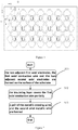
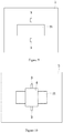
- Figure 1 illustrates a pattern of a traditional capacitive touch device.
- the pattern 10 of the capacitive touch device includes a substrate 5.
- Multiple groups of two adjacent first axial electrodes 1 and a first axial conductive wire 11 constitute sensor electrode units in the X axial direction, which are used for sensing X axial coordinates of touch positions.
- Multiple groups of two adjacent second axial electrodes 2 and a second axial conductive wire 21 constitute sensor electrode units in the Y axial direction, which are used for sensing Y axial coordinates of the touch positions.
- An insulating layer 4 is used for making the first axial conductive wire 11 and the second axial conductive wire 21 electrically insulated from each other.
- the above mentioned sensor electrode units can be made by transparent conductive materials such as Indium Tin Oxide.
- the insulating layer 4 usually is made of transparent insulating materials such as Polyimide.
- Response speed of a capacitive touch device is restricted by resistance of the sensor electrode units in X axial direction and Y axial direction. Resistance of the sensor electrode units is mainly subject to an influence of neck formed by the transparent first axial conductive wire 11. Restricted to the pattern of the traditional capacitive touch devices, area of the first axial conductive wire 11 is usually smaller and at the same time possesses larger resistance. It is therefore a problem to reduce resistance in the neck and improve response speed of the capacitive touch devices.
- US20011/0234511A1 relates to a touch screen panel, wherein a plurality of first connection patterns are arranged on a transparent substrate. On the substrate, a plurality of first sensing cells are electrically connected along a first direction to the first connection patterns, and a plurality of second sensing cells are disposed between the first sensing cells and insulated therefrom. More specifically, the second sensing cells are connected along a second direction by second connection patterns intersecting the first connection patterns, wherein an insulating layer is arranged between the first and second connection patterns, and wherein the second connection patterns overlap the insulation layer.
- conductive auxiliary patterns are arranged at the edges of the insulating layer to be electrically connected to the second connection patterns for reducing the resistance at boundary portions between the second sensing cells and the second connection patterns that cross over the insulation layer.
- the conductive auxiliary patterns are positioned under the second connection patterns or the second sensing cells.
- US2011/0134055A1 relates to a touch panel including a plurality of first sensors disposed on a substrate, wherein a plurality of first electrodes are spaced from one another in a first direction and a first connection pattern connects two adjacent first electrodes.
- a plurality of second sensors are also disposed on the substrate and include a plurality of second electrodes spaced from one another in a second direction, wherein a second connection pattern connect two adjacent second electrodes.
- the first sensor includes a conductive bridge overlapping the first connection pattern for connecting the adjacent first electrodes.
- a metal pattern is arranged to overlap a part of the bridge for reducing the electrical resistance.
- a separate second bridge electrode is arranged on the substrate and connected to adjacent second electrodes.
- US2011/0227839A1 relates to a touch screen panel including first and second sensing cells arranged in different axial directions on a transparent substrate.
- the adjacent second sensing cells are electrically connected by a second connection part arranged on the substrate.
- the adjacent first sensing cells are electrically connected by a first connection part overlapping the second connection part.
- An insulation layer separates the first and second connection parts, and an additional auxiliary pattern is formed underneath the insulating layer and adapted to electrically connect to the adjacent first sensing cells, wherein the additional auxiliary pattern is arranged to be separated from the second connection part on a surface of the substrate.
- CN201465074U relates to a capacitance touch screen wiring structure comprising two groups of transparent conducting films of leads on a substrate.
- An insulating film covers the first group of transparent conducting films of leads on the cross of two groups of transparent conducting films of leads.
- a metal bridging film layer stretches across the insulating film to be connected with the second group of transparent conducting films of leads.
- a capacitive touch pattern formed on a substrate according to the preamble of claim 1 is known from WO 2010/105507 A1 .
- An objective of the present disclosure is to provide a pattern of a capacitive touch device such as detailed in the claims which can effectively reduce resistance of the touch device and enhance response speed of the touch device.
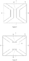
- FIG. 2 shows a flowchart of a manufacturing method of a pattern of a touch device.
- FIG. 3, 4 and 5 are planar figures of patterns produced by the steps in the manufacturing method of FIG. 2 .
- the manufacturing method of patterns of a touch device can either be a yellow-light process or can use a circuit-printing technique.
- the manufacturing method of the pattern of the touch device of the present disclosure comprises; Step S11: forming two adjacent first axial electrodes 1, a first axial conductive wire 11, and two adjacent second axial electrodes 2 on surface of a substrate 5. As shown in FIG. 3 , the first axial conductive wire 11 is set between the two adjacent first axial electrodes 1 to link them together.
- the two adjacent second axial electrodes 2 are disposed separately on two lateral sides of the first axial conductive wire 11.
- the two adjacent first axial electrodes 1, the first axial conductive wire 11, and the two adjacent second axial electrodes 2 can be made from transparent conductive materials.
- the transparent conductive materials have properties of visible light transparency and conductivity.
- the transparent conductive materials can include Indium Tin Oxide, but even other types of transparent conductive materials, not listed here to avoid limitation of disclosure, can also be used.
- the first axial electrodes 1 and the first axial conductive wire 11 can be a structure of integral molding.
- Step S12 covering the first axial conductive wire 11 by an insulating layer 4 as shown in FIG 4 .
- the insulating layer 4 can be made by transparent insulating materials such as Polyimide, but the types of transparent insulating materials are not listed to avoid the limitation of the disclosure.
- Step S13 forming a pair of metal jumpers 3 and a second axial conductive wire 21 as shown in FIG. 5 .
- This pair of metal jumpers 3 is placed on a connection point of two adjacent first axial electrodes 1 and the first axial conductive wire 11.
- the second axial conductive wire 21 across the insulating layer 4 is connected to the two adjacent second axial electrodes 2 making an electrical insulation between the first axial conductive wire 11 and the second axial conductive wire 21.
- Pattern 40 of the touch device in FIG. 5 can be formed through steps S11-S13.
- the first axial conductive wire 11 is narrow and lengthy, and is made of a transparent conductive material, making resistance between the two adjacent first axial electrodes 1 relatively high.
- resistance between the two adjacent first axial electrodes 1 can be reduced and the sensing speed of the integral touch device can be enhanced.
- Pattern 40 of the capacitive touch device can further be connected to an outer controlling unit via peripheral lines with favorable conductivity (not given in FIG. 1 - FIG. 4 ) after completion of the pattern 40 of the touch device.
- peripheral lines with favorable conductivity (not given in FIG. 1 - FIG. 4 ) after completion of the pattern 40 of the touch device.
- first axial peripheral lines (not given in FIG. 1 - FIG.4 ) and second axial peripheral lines (not given in FIG. 2 - FIG. 5 ) are formed on two adjacent lateral sides of the substrate 5 so as to connect the first axial peripheral line with the first axial electrode 1 and connect the second axial peripheral line with the second axial electrode 2.
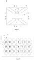
- FIG. 6 is a planar view of the pattern of the capacitive touch device in accordance with the present embodiment.
- Pattern 50 of the touch device is formed by arranging the pattern 40 of the touch device in arrays in FIG. 5 .
- the pattern 40 of the touch device can be finished using the method of the touch device pattern described in the following embodiment.
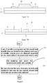
- FIG. 7A shows a cross-sectional view of the pattern 40 of the touch device alongside A axis.
- FIG. 7B is a cross-sectional view of the pattern 40 of the touch device alongside B axis.
- pattern 40 of a touch device includes a substrate 5, two adjacent first axial electrodes 1, a first axial conductive wire 11, two adjacent second axial electrodes 2, a second axial conductive wire 21, an insulating layer 4, and a pair of metal jumpers 3.
- the two adjacent first axial electrodes 1, the first axial conductive wire 11, and the two adjacent second axial electrodes 2 are placed on surface of the substrate 5.
- the first axial conductive wire 11 is formed between the two adjacent first axial electrodes 1 so as to connect them.
- the two adjacent second axial electrodes 2 are disposed separately on two lateral sides of the first axial conductive wire 11.
- the second axial conductive wire 21 stretches across the first axial conductive wire 11 and is connected to the two adjacent second axial electrodes 2.
- the insulating layer 4 is formed between the transparent first axial conductive wire 11 and the second axial conductive wire 21 so as to make them electrically insulated.
- the pair of metal jumpers 3 is placed on the connection point between the two adjacent first axial electrodes 1 and the first axial conductive wire 11.
- multiple groups of the two adjacent first axial electrodes 1 and the first axial conductive wire 11 constitute sensor electrode units in X axial direction.
- the sensor electrode units are used for sensing X axial coordinates of touch positions.
- Multiple groups of two adjacent transparent second axial electrodes 2 and the second axial conductive wire 21 constitute sensor electrode units in Y axial direction, which are used for sensing Y axial coordinates of the touch positions.
- the two adjacent transparent second axial electrodes 2 are composed of transparent conductive materials such as ITO.
- the second axial conductive wire 21 can be a metallic film composed of molybdenum/ aluminum /molybdenum or any other metal with good conductivity. The metallic film of molybdenum / aluminum/molybdenum is suitable being used in the etching process to finish the second axial conductive wire 21.
- the insulating layer 4 is formed between the transparent first axial conductive wire 11 and the second axial conductive wire 21. Based on width of the second axial conductive wire 21, an insulating layer with a proper area can be selected so that appropriate electrical insulation can be made between the first axial conductive wire 11 and the second axial conductive wire 21.
- the insulating layer 4 can be made of a Polyimide or any other compatible/well known material.
- a pair of metal jumpers 3 is used for reducing resistance of the electrode units in X axial direction constituted by the transparent first axial electrode 1 and the transparent first axial conductive wire 11.
- the pair of metal jumpers 3 can be located near the connection point of the two adjacent first axial electrodes 1 and the first conductive wire 11.
- the first axial conductive wire 11 has relatively a small cross section compared to that of the first axial electrode 1, which makes resistance of neck, which includes the two adjacent first axial electrodes 1 and the first axial conductive wire 11, larger. This increases resistance of the electrode units of the X axial direction constituted by the first axial electrode 1 and the transparent first axial conductive wire 11.
- Resistance of electrode units of X axial direction that comprise of the first axial electrode 1 and of the transparent conductive wire 11 can be reduced via a pair of metallic conductive wires 3. Reduction of this resistance can shorten the response time of the touch device, thereby enhancing response speed of the touch device.
- a method to calculate resistance of the X axial electrode units is mentioned herein.
- value of the first axial electrodes 1 is represented by N, then N-1 represents the number of the first axial conductive wires 11.
- Resistance of the electrode units of the X axial direction represents resistance acquired from serial wounding of the first axial electrode 1 and the first axial conductive wire 11.
- resistance of the electrode units of the X axial direction is the resistance of the first axial electrode 1 multiplied by number of the first axial electrodes 1 and then next adding resistance of the neck, which constitutes the two adjacent first axial electrodes and the first axial conductive wire 11, and then finally multiplying the number of the necks.
- resistance of each first axial electrode 1 is 100 ⁇ , and the resistance of each individual neck is 200 ⁇ .
- N is 11
- resistance of the neck becomes 10 ⁇ .
- a pair of metal jumpers 3 can comprise of any metallic conductive wire, and more specifically a metallic film that comprises of molybdenum, aluminum, or molybdenum. Using an etching process, the pair of metal jumpers 3 and the second axial conductive wire 21 can be finished.
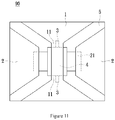
- FIG. 8 shows a flowchart of a manufacturing method of the touch device pattern.
- FIG. 9 - FIG. 11 are schematic diagrams of structures corresponding to various steps in the manufacturing method of the touch device pattern.
- the manufacturing method of the touch device pattern can be a yellow-light process or a circuit-printing technique.
- the touch device pattern 90 produced in the manufacturing method of the touch device pattern, has structure of an adverse superposition of the touch device pattern 40.
- the manufacturing method of the touch device pattern comprises; Step S61: forming a pair of metal jumpers 3 and a second axial conductive wire 21 on a substrate 5, wherein the pair of metal jumpers 3 is disposed separately on two lateral sides of the second axial conductive wire 21, as shown in FIG. 9 .
- the pair of metal jumpers 3 and the second axial conductive wire 21 can be made of a metallic film of molybdenum/ aluminum/ molybdenum.
- Step S62 covering the second axial conductive wire 21 by an insulating layer 4, as shown in FIG. 10 .
- the insulating layer 4 can be a Polyimide, but the disclosure is not confined to this.
- Step S63 forming two adjacent first axial electrodes 1, a first axial conductive wire 11, and two adjacent second axial electrodes 2 on a substrate 50.
- the two adjacent second axial electrodes 2 are connected to both ends of the second axial conductive wire 21.
- the two adjacent first axial electrodes 1 are disposed separately on two lateral sides of the second axial conductive wire 21.
- the first axial conductive wire 11 is covered partially over the insulating layer 4 and partially over the pair of metal jumpers 3.
- the first axial conductive wire 11 is connected to the two adjacent first axial electrodes 1.
- the insulating layer 4 positioned between the first axial conductive wire 11 and the second axial conductive wire 21 makes the wires 11 and 21 electrically insulated.
- the two adjacent first axial electrodes 1, the first axial conductive wire 11, and the two adjacent second axial electrodes 2 can be made of Indium Tin Oxide.
- the touch control circuit pattern 90 is formed via steps S61 - S63.
- the touch device pattern of the present disclosure and its manufacturing method reduces the resistance caused by a neck, which comprises of two adjacent first axial electrodes and a first axial conductive wire, thereby enhancing response speed of the touch device pattern.
Description
- This disclosure generally relates to a touch device, and more particularly to pattern of a capacitive touch device and a manufacturing method thereof.
- With the rapid development of the electronic materials, touch devices have already become a commonly used input interface. Traditional input device, depending on pressure or manual operation, may also be replaced by a touch device in near future. More recently, due to prosperous development of liquid crystal panels, display screen integrated touch devices have already been produced and sold in large amounts. Touch devices can be divided into resistive touch devices and capacitive touch devices. Existing consumer electronic products have substantially taken advantage of capacitive touch devices and have integrated the capacitive devices with the display screens.
- Capacitive touch devices in integrated display screens usually have a coordinate-sensing capacity for two axial directions on the flat surface (X axis and Y axis).
Figure 1 illustrates a pattern of a traditional capacitive touch device. Thepattern 10 of the capacitive touch device includes asubstrate 5. Multiple groups of two adjacent firstaxial electrodes 1 and a first axialconductive wire 11 constitute sensor electrode units in the X axial direction, which are used for sensing X axial coordinates of touch positions. Multiple groups of two adjacent secondaxial electrodes 2 and a second axialconductive wire 21 constitute sensor electrode units in the Y axial direction, which are used for sensing Y axial coordinates of the touch positions. Aninsulating layer 4 is used for making the first axialconductive wire 11 and the second axialconductive wire 21 electrically insulated from each other. The above mentioned sensor electrode units can be made by transparent conductive materials such as Indium Tin Oxide. - The insulating
layer 4 usually is made of transparent insulating materials such as Polyimide. Response speed of a capacitive touch device is restricted by resistance of the sensor electrode units in X axial direction and Y axial direction. Resistance of the sensor electrode units is mainly subject to an influence of neck formed by the transparent first axialconductive wire 11. Restricted to the pattern of the traditional capacitive touch devices, area of the first axialconductive wire 11 is usually smaller and at the same time possesses larger resistance. It is therefore a problem to reduce resistance in the neck and improve response speed of the capacitive touch devices. -
US20011/0234511A1 -
US2011/0134055A1 relates to a touch panel including a plurality of first sensors disposed on a substrate, wherein a plurality of first electrodes are spaced from one another in a first direction and a first connection pattern connects two adjacent first electrodes. A plurality of second sensors are also disposed on the substrate and include a plurality of second electrodes spaced from one another in a second direction, wherein a second connection pattern connect two adjacent second electrodes. For this purpose, the first sensor includes a conductive bridge overlapping the first connection pattern for connecting the adjacent first electrodes. A metal pattern is arranged to overlap a part of the bridge for reducing the electrical resistance. A separate second bridge electrode is arranged on the substrate and connected to adjacent second electrodes. -
US2011/0227839A1 relates to a touch screen panel including first and second sensing cells arranged in different axial directions on a transparent substrate. The adjacent second sensing cells are electrically connected by a second connection part arranged on the substrate. The adjacent first sensing cells are electrically connected by a first connection part overlapping the second connection part. An insulation layer separates the first and second connection parts, and an additional auxiliary pattern is formed underneath the insulating layer and adapted to electrically connect to the adjacent first sensing cells, wherein the additional auxiliary pattern is arranged to be separated from the second connection part on a surface of the substrate. -
CN201465074U relates to a capacitance touch screen wiring structure comprising two groups of transparent conducting films of leads on a substrate. An insulating film covers the first group of transparent conducting films of leads on the cross of two groups of transparent conducting films of leads. A metal bridging film layer stretches across the insulating film to be connected with the second group of transparent conducting films of leads. - A capacitive touch pattern formed on a substrate according to the preamble of
claim 1 is known fromWO 2010/105507 A1 . - An objective of the present disclosure is to provide a pattern of a capacitive touch device such as detailed in the claims which can effectively reduce resistance of the touch device and enhance response speed of the touch device.
-
-
FIG. 1 shows a traditional touch device pattern. -
Fig. 2 shows flowchart of a manufacturing method of a touch device pattern in accordance with an embodiment of the present disclosure . -
FIG. 3-FIG. 5 illustrate structures corresponding to various steps in the manufacturing method of the touch device pattern in accordance with the embodiment of the present disclosure . -
FIG. 6 is illustrates a schematic diagram of the touch device pattern in accordance with the embodiment of the present disclosure . -
FIG. 7A is a cross-sectional figure of a touch device pattern along A axis. -
FIG. 7B is a cross-sectional figure of a touch device pattern along B axis. -
FIG. 8 shows a flowchart of a manufacturing method of a touch device pattern. -
FIG. 9-FIG. 11 are schematic diagrams of structures corresponding to various steps in the manufacturing method of the touch device pattern. - For those skilled in the art, embodiments, examples not covered by the claims and drawings described below are for illustration purposes only and do not limit the scope of the present disclosure in any manner.
-
FIG. 2 shows a flowchart of a manufacturing method of a pattern of a touch device.FIG. 3, 4 and5 are planar figures of patterns produced by the steps in the manufacturing method ofFIG. 2 . The manufacturing method of patterns of a touch device can either be a yellow-light process or can use a circuit-printing technique. The manufacturing method of the pattern of the touch device of the present disclosure comprises;
Step S11: forming two adjacent firstaxial electrodes 1, a first axialconductive wire 11, and two adjacent secondaxial electrodes 2 on surface of asubstrate 5. As shown inFIG. 3 , the first axialconductive wire 11 is set between the two adjacent firstaxial electrodes 1 to link them together. The two adjacent secondaxial electrodes 2 are disposed separately on two lateral sides of the first axialconductive wire 11. The two adjacent firstaxial electrodes 1, the first axialconductive wire 11, and the two adjacent secondaxial electrodes 2 can be made from transparent conductive materials. The transparent conductive materials have properties of visible light transparency and conductivity. The transparent conductive materials can include Indium Tin Oxide, but even other types of transparent conductive materials, not listed here to avoid limitation of disclosure, can also be used. The firstaxial electrodes 1 and the first axialconductive wire 11 can be a structure of integral molding. - Step S12: covering the first axial
conductive wire 11 by aninsulating layer 4 as shown inFIG 4 . The insulatinglayer 4 can be made by transparent insulating materials such as Polyimide, but the types of transparent insulating materials are not listed to avoid the limitation of the disclosure. - Step S13: forming a pair of
metal jumpers 3 and a second axialconductive wire 21 as shown inFIG. 5 . This pair ofmetal jumpers 3 is placed on a connection point of two adjacent firstaxial electrodes 1 and the first axialconductive wire 11. The second axialconductive wire 21 across the insulatinglayer 4 is connected to the two adjacent secondaxial electrodes 2 making an electrical insulation between the first axialconductive wire 11 and the second axialconductive wire 21.Pattern 40 of the touch device inFIG. 5 can be formed through steps S11-S13. - In
pattern 40 of the capacitive touch device inFIG. 5 , the first axialconductive wire 11 is narrow and lengthy, and is made of a transparent conductive material, making resistance between the two adjacent firstaxial electrodes 1 relatively high. However, after the pair ofmetal jumpers 3 is disposed on the connection point between the two adjacent firstaxial electrodes 1 and the first axialconductive wire 11, resistance between the two adjacent firstaxial electrodes 1 can be reduced and the sensing speed of the integral touch device can be enhanced. -
Pattern 40 of the capacitive touch device can further be connected to an outer controlling unit via peripheral lines with favorable conductivity (not given inFIG. 1 - FIG. 4 ) after completion of thepattern 40 of the touch device. For illustration, first axial peripheral lines (not given inFIG. 1 - FIG.4 ) and second axial peripheral lines (not given inFIG. 2 - FIG. 5 ) are formed on two adjacent lateral sides of thesubstrate 5 so as to connect the first axial peripheral line with the firstaxial electrode 1 and connect the second axial peripheral line with the secondaxial electrode 2. -
FIG. 6 is a planar view of the pattern of the capacitive touch device in accordance with the present embodiment.Pattern 50 of the touch device is formed by arranging thepattern 40 of the touch device in arrays inFIG. 5 . Thepattern 40 of the touch device can be finished using the method of the touch device pattern described in the following embodiment. -
FIG. 7A shows a cross-sectional view of thepattern 40 of the touch device alongside A axis.FIG. 7B is a cross-sectional view of thepattern 40 of the touch device alongside B axis. In an embodiment,pattern 40 of a touch device includes asubstrate 5, two adjacent firstaxial electrodes 1, a first axialconductive wire 11, two adjacent secondaxial electrodes 2, a second axialconductive wire 21, an insulatinglayer 4, and a pair ofmetal jumpers 3. The two adjacent firstaxial electrodes 1, the first axialconductive wire 11, and the two adjacent secondaxial electrodes 2 are placed on
surface of thesubstrate 5. The first axialconductive wire 11 is formed between the two adjacent firstaxial electrodes 1 so as to connect them. The two adjacent secondaxial electrodes 2 are disposed separately on two lateral sides of the first axialconductive wire 11. The second axialconductive wire 21 stretches across the first axialconductive wire 11 and is connected to the two adjacent secondaxial electrodes 2. The insulatinglayer 4 is formed between the transparent first axialconductive wire 11 and the second axialconductive wire 21 so as to make them electrically insulated. The pair ofmetal jumpers 3 is placed on the connection point between the two adjacent firstaxial electrodes 1 and the first axialconductive wire 11. - Referring to
FIG. 5 and FIG. 6 , multiple groups of the two adjacent firstaxial electrodes 1 and the first axialconductive wire 11 constitute sensor electrode units in X axial direction. The sensor electrode units are used for sensing X axial coordinates of touch positions. Multiple groups of two adjacent transparent secondaxial electrodes 2 and the second axialconductive wire 21 constitute sensor electrode units in Y axial direction, which are used for sensing Y axial coordinates of the touch positions. The two adjacent transparent secondaxial electrodes 2 are composed of transparent conductive materials such as ITO. The second axialconductive wire 21 can be a metallic film composed of molybdenum/ aluminum /molybdenum or any other metal with good conductivity. The metallic film of molybdenum / aluminum/molybdenum is suitable being used in the etching process to finish the second axialconductive wire 21. - The insulating
layer 4 is formed between the transparent first axialconductive wire 11 and the second axialconductive wire 21. Based on width of the second axialconductive wire 21, an insulating layer with a proper area can be selected so that appropriate electrical insulation can be made between the first axialconductive wire 11 and the second axialconductive wire 21. The insulatinglayer 4 can be made of a Polyimide or any other compatible/well known material. - A pair of
metal jumpers 3 is used for reducing resistance of the electrode units in X axial direction constituted by the transparent firstaxial electrode 1 and the transparent first axialconductive wire 11. The pair ofmetal jumpers 3 can be located near the connection point of the two adjacent firstaxial electrodes 1 and the firstconductive wire 11. The first axialconductive wire 11 has relatively a small cross section compared to that of the firstaxial electrode 1, which makes resistance of neck, which includes the two adjacent firstaxial electrodes 1 and the first axialconductive wire 11, larger. This increases resistance of the electrode units of the X axial direction constituted by the firstaxial electrode 1 and the transparent first axialconductive wire 11. - Resistance of electrode units of X axial direction that comprise of the first
axial electrode 1 and of the transparentconductive wire 11 can be reduced via a pair of metallicconductive wires 3. Reduction of this resistance can shorten the response time of the touch device, thereby enhancing response speed of the touch device. A method to calculate resistance of the X axial electrode units is mentioned herein. When value of the firstaxial electrodes 1 is represented by N, then N-1 represents the number of the first axialconductive wires 11. Resistance of the electrode units of the X axial direction represents resistance acquired from serial wounding of the firstaxial electrode 1 and the first axialconductive wire 11. In other words, resistance of the electrode units of the X axial direction is the resistance of the firstaxial electrode 1 multiplied by number of the firstaxial electrodes 1 and then next adding resistance of the neck, which constitutes the two adjacent first axial electrodes and the first axialconductive wire 11, and then finally multiplying the number of the necks. - Illustratively, resistance of each first
axial electrode 1 is 100Ω, and the resistance of each individual neck is 200Ω. When N is 11, resistance of the electrode units of the X axial direction is equivalent to 3100Ω (11×100+10×200=3100Ω). Assuming that after adding a pair of metallicconductive wires 3, resistance of the neck becomes 10Ω. Then, resistance of the electrode units of the X axial direction is equivalent to 1200Ω. (11×100+10×10=1200Ω). - A pair of
metal jumpers 3 can comprise of any metallic conductive wire, and more specifically a metallic film that comprises of molybdenum, aluminum, or molybdenum. Using an etching process, the pair ofmetal jumpers 3 and the second axialconductive wire 21 can be finished. -
FIG. 8 shows a flowchart of a manufacturing method of the touch device pattern.FIG. 9 - FIG. 11 are schematic diagrams of structures corresponding to various steps in the manufacturing method of the touch device pattern. The manufacturing method of the touch device pattern can be a yellow-light process or a circuit-printing technique. As shown inFIG. 11 , thetouch device pattern 90, produced in the manufacturing method of the touch device pattern, has structure of an adverse superposition of thetouch device pattern 40. The manufacturing method of the touch device pattern comprises;
Step S61: forming a pair ofmetal jumpers 3 and a second axialconductive wire 21 on asubstrate 5, wherein the pair ofmetal jumpers 3 is disposed separately on two lateral sides of the second axialconductive wire 21, as shown inFIG. 9 . The pair ofmetal jumpers 3 and the second axialconductive wire 21 can be made of a metallic film of molybdenum/ aluminum/ molybdenum. - Step S62: covering the second axial
conductive wire 21 by an insulatinglayer 4, as shown inFIG. 10 . The insulatinglayer 4 can be a Polyimide, but the disclosure is not confined to this. - Step S63: forming two adjacent first
axial electrodes 1, a first axialconductive wire 11, and two adjacent secondaxial electrodes 2 on asubstrate 50. As shown inFIG. 11 , the two adjacent secondaxial electrodes 2 are connected to both ends of the second axialconductive wire 21. The two adjacent firstaxial electrodes 1 are disposed separately on two lateral sides of the second axialconductive wire 21. The first axialconductive wire 11 is covered partially over the insulatinglayer 4 and partially over the pair ofmetal jumpers 3. The first axialconductive wire 11 is connected to the two adjacent firstaxial electrodes 1. The insulatinglayer 4 positioned between the first axialconductive wire 11 and the second axialconductive wire 21 makes thewires axial electrodes 1, the first axialconductive wire 11, and the two adjacent secondaxial electrodes 2 can be made of Indium Tin Oxide. The touchcontrol circuit pattern 90 is formed via steps S61 - S63. - In accordance with the embodiments and the examples not covered by the claims, the touch device pattern of the present disclosure and its manufacturing method reduces the resistance caused by a neck, which comprises of two adjacent first axial electrodes and a first axial conductive wire, thereby enhancing response speed of the touch device pattern.
Claims (5)
- A capacitive touch device comprising: a pattern formed on a substrate, comprising:two adjacent first electrodes (1) arranged in a first axial direction;a first conductive wire (11) integrally formed with said two adjacent first electrodes (1) on a surface of the substrate (5) to contact the first electrodes (1), wherein the first electrodes (1) and the first conductive wire (11) are made of a transparent conductive material such as ITO; two adjacent transparent second electrodes made of a transparent conductive material such as ITO arranged in a second axial direction and disposed separately on two lateral sides of the first conductive wire (11);a second conductive wire (21) made of metal formed across the first conductive wire (11) for connecting said two adjacent second electrodes (2); andan insulating layer (4) formed between said first conductive wire (11) and said second conductive wire (21) and covering said first conductive wire (11) partially to electrically insulate said first conductive wire (11) and said second conductive wire (21); characterized bya pair of metal conductors (3) electrically connected to and arranged on said two adjacent first electrodes (1) and said first conductive wire (11) across connection points of said two adjacent first electrodes (1) and said first conductive wire (11), wherein said pair of metal conductors (3) is manufactured in a same manufacturing step as said second conductive wire (21).
- The capacitive touch device as claimed in claim 1, wherein said pair of metal conductors (3) and the second conductive wire (21) are made from molybdenum/aluminum molybdenum.
- The capacitive touch device as claimed in claim 1, wherein
said capacitive touch device pattern further comprises:
a first peripheral line and a second peripheral line placed on two adjacent sides of the substrate (5), wherein said first peripheral line is connected to said first electrodes (1), and wherein said second peripheral line is connected to said second electrodes (2). - A manufacturing method of a capacitive touch device comprising the steps of:forming two adjacent first electrodes (1) arranged in a first axial direction, a first conductive wire (11), and two adjacent second electrodes (2) arranged in a second axial direction on a surface of a substrate (5), (S11), wherein said first conductive wire (11) is formed together with the two adjacent first electrodes (1) of a transparent conductive material such as ITO on the surface of the substrate (5) to connect them in a single manufacturing step, further wherein the two adjacent second electrodes (1) made of a transparent conductive oxide such as ITO are disposed separately on two lateral sides of the first conductive wire (11);forming an insulating layer (4) to partially cover the first conductive wire (S12); andforming a pair of metal conductors (3) and a second conductive wire (21) of metal, in a same manufacturing step (S13), wherein said second conductive wire (21) connects the two adjacent second electrodes (2), and wherein said pair of metal conductors (3) are electrically connected to and arranged on said two adjacent first electrodes (1) and said first conductive wire (11) across connection points of the two adjacent first electrodes (1) and said first conductive wire (11).wherein said second conductive wire (21) is formed across said insulating layer (4) and wherein said insulating layer (4) electrically insulates the first conductive wire (11) and the second conductive wire (21).
- The manufacturing method of claim 4, further comprising:
forming a first peripheral line and a second peripheral line on sides of the substrate (5), wherein the first peripheral line is connected to the first electrodes (1) and the second peripheral line is connected to the second electrodes (2).
Applications Claiming Priority (2)
| Application Number | Priority Date | Filing Date | Title |
|---|---|---|---|
| CN2011103175428A CN103049144A (en) | 2011-10-14 | 2011-10-14 | Touch control device figure and manufacture method thereof |
| PCT/CN2012/079908 WO2013053263A1 (en) | 2011-10-14 | 2012-08-10 | Pattern of a capacitive touch device and manufacturing method thereof |
Publications (3)
| Publication Number | Publication Date |
|---|---|
| EP2766800A1 EP2766800A1 (en) | 2014-08-20 |
| EP2766800A4 EP2766800A4 (en) | 2015-06-17 |
| EP2766800B1 true EP2766800B1 (en) | 2019-09-18 |
Family
ID=47048794
Family Applications (1)
| Application Number | Title | Priority Date | Filing Date |
|---|---|---|---|
| EP12840406.8A Active EP2766800B1 (en) | 2011-10-14 | 2012-08-10 | Pattern of a capacitive touch device and manufacturing method thereof |
Country Status (7)
| Country | Link |
|---|---|
| US (1) | US9619085B2 (en) |
| EP (1) | EP2766800B1 (en) |
| JP (1) | JP2015507231A (en) |
| KR (1) | KR20140069319A (en) |
| CN (1) | CN103049144A (en) |
| TW (2) | TWM435666U (en) |
| WO (1) | WO2013053263A1 (en) |
Families Citing this family (5)
| Publication number | Priority date | Publication date | Assignee | Title |
|---|---|---|---|---|
| CN103049144A (en) * | 2011-10-14 | 2013-04-17 | 宸鸿科技(厦门)有限公司 | Touch control device figure and manufacture method thereof |
| CN104007860B (en) * | 2013-02-22 | 2017-02-08 | 宸美(厦门)光电有限公司 | Touchpad structure and manufacturing method thereof |
| KR102177716B1 (en) | 2013-12-30 | 2020-11-11 | 엘지디스플레이 주식회사 | Touch sensor integrated display device |
| CN104777924B (en) * | 2014-01-09 | 2018-03-02 | 宸鸿科技(厦门)有限公司 | Contact panel and preparation method thereof |
| CN106033275B (en) * | 2015-03-18 | 2019-10-18 | 宸鸿科技(厦门)有限公司 | Touch panel and its manufacturing method |
Citations (1)
| Publication number | Priority date | Publication date | Assignee | Title |
|---|---|---|---|---|
| WO2010105507A1 (en) * | 2009-03-20 | 2010-09-23 | 宸鸿科技(厦门)有限公司 | Capacitive touch circuit pattern and manufacturing method thereof |
Family Cites Families (19)
| Publication number | Priority date | Publication date | Assignee | Title |
|---|---|---|---|---|
| CN101526869B (en) | 2008-03-07 | 2012-05-02 | 达诺光电股份有限公司 | Touch panel with improved electrode patterns |
| KR101073285B1 (en) * | 2008-12-01 | 2011-10-12 | 삼성모바일디스플레이주식회사 | Touch Screen Panel |
| CN201465074U (en) | 2009-02-28 | 2010-05-12 | 成都吉锐触摸技术股份有限公司 | Multi-point touch infrared touch screen |
| KR100944519B1 (en) | 2009-03-04 | 2010-03-03 | 남동식 | Touch panel sensor |
| CN101840292B (en) * | 2009-03-20 | 2011-12-21 | 宸鸿科技(厦门)有限公司 | Capacitance type touch control circuit pattern and manufacturing method thereof |
| CN101859213B (en) * | 2009-04-13 | 2012-08-29 | 群康科技(深圳)有限公司 | Making method of capacitor-type touch panel |
| CN201465084U (en) | 2009-06-05 | 2010-05-12 | 深圳莱宝高科技股份有限公司 | Capacitance touch screen wiring structure |
| KR101464818B1 (en) * | 2009-06-23 | 2014-11-25 | 지오마텍 가부시키가이샤 | Capacitance type input device and production method thereof |
| JP5473460B2 (en) * | 2009-07-30 | 2014-04-16 | 京セラ株式会社 | Input device and display device including the input device |
| CN102023770B (en) * | 2009-09-22 | 2013-02-27 | 群康科技(深圳)有限公司 | Capacitive touch panel module and manufacturing method thereof |
| US8970509B2 (en) * | 2009-12-09 | 2015-03-03 | Lg Display Co., Ltd. | Touch panel and liquid crystal display device including the same |
| TWI396901B (en) * | 2009-12-21 | 2013-05-21 | Au Optronics Corp | Method of fabricating touch panel |
| KR101048948B1 (en) * | 2010-02-22 | 2011-07-12 | 삼성모바일디스플레이주식회사 | Fabricating method for touch screen panel |
| KR101040846B1 (en) * | 2010-03-16 | 2011-06-14 | 삼성모바일디스플레이주식회사 | Touch screen panel and fabrication method thereof |
| KR101101053B1 (en) * | 2010-03-16 | 2011-12-29 | 삼성모바일디스플레이주식회사 | Touch Screen Panel and fabrication method thereof |
| KR101040851B1 (en) * | 2010-03-23 | 2011-06-14 | 삼성모바일디스플레이주식회사 | Touch screen panel |
| CN101957700A (en) * | 2010-09-30 | 2011-01-26 | 深圳市中显微电子有限公司 | Touch pad of capacitive touch screen and manufacturing method thereof |
| CN202351844U (en) * | 2011-10-14 | 2012-07-25 | 宸鸿科技(厦门)有限公司 | Touch control device pattern |
| CN103049144A (en) * | 2011-10-14 | 2013-04-17 | 宸鸿科技(厦门)有限公司 | Touch control device figure and manufacture method thereof |
-
2011
- 2011-10-14 CN CN2011103175428A patent/CN103049144A/en active Pending
-
2012
- 2012-02-15 TW TW101202737U patent/TWM435666U/en unknown
- 2012-02-15 TW TW101104894A patent/TWI494831B/en active
- 2012-07-05 US US13/541,768 patent/US9619085B2/en active Active
- 2012-08-10 WO PCT/CN2012/079908 patent/WO2013053263A1/en active Application Filing
- 2012-08-10 EP EP12840406.8A patent/EP2766800B1/en active Active
- 2012-08-10 KR KR1020147011526A patent/KR20140069319A/en not_active Application Discontinuation
- 2012-08-10 JP JP2014533758A patent/JP2015507231A/en active Pending
Patent Citations (2)
| Publication number | Priority date | Publication date | Assignee | Title |
|---|---|---|---|---|
| WO2010105507A1 (en) * | 2009-03-20 | 2010-09-23 | 宸鸿科技(厦门)有限公司 | Capacitive touch circuit pattern and manufacturing method thereof |
| EP2410411A1 (en) * | 2009-03-20 | 2012-01-25 | TPK Touch Solutions (Xiamen) Inc. | Capacitive touch circuit pattern and manufacturing method thereof |
Also Published As
| Publication number | Publication date |
|---|---|
| TW201316233A (en) | 2013-04-16 |
| CN103049144A (en) | 2013-04-17 |
| US20130093718A1 (en) | 2013-04-18 |
| TWM435666U (en) | 2012-08-11 |
| EP2766800A1 (en) | 2014-08-20 |
| EP2766800A4 (en) | 2015-06-17 |
| JP2015507231A (en) | 2015-03-05 |
| US9619085B2 (en) | 2017-04-11 |
| KR20140069319A (en) | 2014-06-09 |
| WO2013053263A1 (en) | 2013-04-18 |
| TWI494831B (en) | 2015-08-01 |
Similar Documents
| Publication | Publication Date | Title |
|---|---|---|
| US9857922B2 (en) | Touch panel and manufacturing method thereof | |
| KR101180818B1 (en) | Touch panel device | |
| US9153385B2 (en) | Electrode structure of the touch panel, method thereof and touch panel | |
| US9832861B2 (en) | Touch panel and manufacturing method thereof | |
| KR101323004B1 (en) | Capacity type touch screen panel | |
| KR102194607B1 (en) | Touch screen panel | |
| EP2766800B1 (en) | Pattern of a capacitive touch device and manufacturing method thereof | |
| US20130153391A1 (en) | Capacitive touch panel | |
| US20160041647A1 (en) | Touch screen panel fabrication method and touch screen panel | |
| CN103064551A (en) | Touch sensing device and manufacturing method thereof | |
| TWI463363B (en) | Touch-control pattern structure, manufacture method thereof and touch panel containing therein | |
| EP2690534B1 (en) | Touch screen panel and fabrication method thereof | |
| TWI588688B (en) | Touch panel and touch display panel | |
| TW200945149A (en) | Wiring structure of capacitive touch panel | |
| US9459735B2 (en) | Electrode pattern structure of a capacitive touch panel and method of manufacturing the same | |
| KR102254179B1 (en) | Touch display apparatus | |
| KR20140059571A (en) | Touch panel and method for manufacturing the same | |
| TWI354924B (en) | ||
| TWI403945B (en) | Capacitive touch circuit and its manufacturing method | |
| TWI510985B (en) | Touch screen module | |
| CN204515729U (en) | Contact panel | |
| CN202133986U (en) | Touch-control pattern structure and touch panel | |
| CN202394195U (en) | Touch control panel | |
| TWI640910B (en) | Display screen, capacitive touch circuit and manufacturing method thereof |
Legal Events
| Date | Code | Title | Description |
|---|---|---|---|
| PUAI | Public reference made under article 153(3) epc to a published international application that has entered the european phase |
Free format text: ORIGINAL CODE: 0009012 |
|
| 17P | Request for examination filed |
Effective date: 20140407 |
|
| AK | Designated contracting states |
Kind code of ref document: A1 Designated state(s): AL AT BE BG CH CY CZ DE DK EE ES FI FR GB GR HR HU IE IS IT LI LT LU LV MC MK MT NL NO PL PT RO RS SE SI SK SM TR |
|
| DAX | Request for extension of the european patent (deleted) | ||
| RA4 | Supplementary search report drawn up and despatched (corrected) |
Effective date: 20150515 |
|
| RIC1 | Information provided on ipc code assigned before grant |
Ipc: G06F 3/044 20060101AFI20150508BHEP |
|
| 17Q | First examination report despatched |
Effective date: 20160105 |
|
| STAA | Information on the status of an ep patent application or granted ep patent |
Free format text: STATUS: EXAMINATION IS IN PROGRESS |
|
| GRAP | Despatch of communication of intention to grant a patent |
Free format text: ORIGINAL CODE: EPIDOSNIGR1 |
|
| STAA | Information on the status of an ep patent application or granted ep patent |
Free format text: STATUS: GRANT OF PATENT IS INTENDED |
|
| INTG | Intention to grant announced |
Effective date: 20190322 |
|
| GRAJ | Information related to disapproval of communication of intention to grant by the applicant or resumption of examination proceedings by the epo deleted |
Free format text: ORIGINAL CODE: EPIDOSDIGR1 |
|
| STAA | Information on the status of an ep patent application or granted ep patent |
Free format text: STATUS: EXAMINATION IS IN PROGRESS |
|
| GRAR | Information related to intention to grant a patent recorded |
Free format text: ORIGINAL CODE: EPIDOSNIGR71 |
|
| GRAS | Grant fee paid |
Free format text: ORIGINAL CODE: EPIDOSNIGR3 |
|
| STAA | Information on the status of an ep patent application or granted ep patent |
Free format text: STATUS: GRANT OF PATENT IS INTENDED |
|
| INTC | Intention to grant announced (deleted) | ||
| GRAA | (expected) grant |
Free format text: ORIGINAL CODE: 0009210 |
|
| STAA | Information on the status of an ep patent application or granted ep patent |
Free format text: STATUS: THE PATENT HAS BEEN GRANTED |
|
| AK | Designated contracting states |
Kind code of ref document: B1 Designated state(s): AL AT BE BG CH CY CZ DE DK EE ES FI FR GB GR HR HU IE IS IT LI LT LU LV MC MK MT NL NO PL PT RO RS SE SI SK SM TR |
|
| INTG | Intention to grant announced |
Effective date: 20190813 |
|
| REG | Reference to a national code |
Ref country code: GB Ref legal event code: FG4D |
|
| REG | Reference to a national code |
Ref country code: CH Ref legal event code: EP |
|
| REG | Reference to a national code |
Ref country code: DE Ref legal event code: R096 Ref document number: 602012064188 Country of ref document: DE |
|
| REG | Reference to a national code |
Ref country code: AT Ref legal event code: REF Ref document number: 1182100 Country of ref document: AT Kind code of ref document: T Effective date: 20191015 |
|
| REG | Reference to a national code |
Ref country code: IE Ref legal event code: FG4D |
|
| REG | Reference to a national code |
Ref country code: NL Ref legal event code: FP |
|
| PG25 | Lapsed in a contracting state [announced via postgrant information from national office to epo] |
Ref country code: SE Free format text: LAPSE BECAUSE OF FAILURE TO SUBMIT A TRANSLATION OF THE DESCRIPTION OR TO PAY THE FEE WITHIN THE PRESCRIBED TIME-LIMIT Effective date: 20190918 Ref country code: HR Free format text: LAPSE BECAUSE OF FAILURE TO SUBMIT A TRANSLATION OF THE DESCRIPTION OR TO PAY THE FEE WITHIN THE PRESCRIBED TIME-LIMIT Effective date: 20190918 Ref country code: NO Free format text: LAPSE BECAUSE OF FAILURE TO SUBMIT A TRANSLATION OF THE DESCRIPTION OR TO PAY THE FEE WITHIN THE PRESCRIBED TIME-LIMIT Effective date: 20191218 Ref country code: BG Free format text: LAPSE BECAUSE OF FAILURE TO SUBMIT A TRANSLATION OF THE DESCRIPTION OR TO PAY THE FEE WITHIN THE PRESCRIBED TIME-LIMIT Effective date: 20191218 Ref country code: LT Free format text: LAPSE BECAUSE OF FAILURE TO SUBMIT A TRANSLATION OF THE DESCRIPTION OR TO PAY THE FEE WITHIN THE PRESCRIBED TIME-LIMIT Effective date: 20190918 Ref country code: FI Free format text: LAPSE BECAUSE OF FAILURE TO SUBMIT A TRANSLATION OF THE DESCRIPTION OR TO PAY THE FEE WITHIN THE PRESCRIBED TIME-LIMIT Effective date: 20190918 |
|
| REG | Reference to a national code |
Ref country code: LT Ref legal event code: MG4D |
|
| PG25 | Lapsed in a contracting state [announced via postgrant information from national office to epo] |
Ref country code: AL Free format text: LAPSE BECAUSE OF FAILURE TO SUBMIT A TRANSLATION OF THE DESCRIPTION OR TO PAY THE FEE WITHIN THE PRESCRIBED TIME-LIMIT Effective date: 20190918 Ref country code: LV Free format text: LAPSE BECAUSE OF FAILURE TO SUBMIT A TRANSLATION OF THE DESCRIPTION OR TO PAY THE FEE WITHIN THE PRESCRIBED TIME-LIMIT Effective date: 20190918 Ref country code: GR Free format text: LAPSE BECAUSE OF FAILURE TO SUBMIT A TRANSLATION OF THE DESCRIPTION OR TO PAY THE FEE WITHIN THE PRESCRIBED TIME-LIMIT Effective date: 20191219 Ref country code: RS Free format text: LAPSE BECAUSE OF FAILURE TO SUBMIT A TRANSLATION OF THE DESCRIPTION OR TO PAY THE FEE WITHIN THE PRESCRIBED TIME-LIMIT Effective date: 20190918 |
|
| REG | Reference to a national code |
Ref country code: AT Ref legal event code: MK05 Ref document number: 1182100 Country of ref document: AT Kind code of ref document: T Effective date: 20190918 |
|
| PG25 | Lapsed in a contracting state [announced via postgrant information from national office to epo] |
Ref country code: ES Free format text: LAPSE BECAUSE OF FAILURE TO SUBMIT A TRANSLATION OF THE DESCRIPTION OR TO PAY THE FEE WITHIN THE PRESCRIBED TIME-LIMIT Effective date: 20190918 Ref country code: RO Free format text: LAPSE BECAUSE OF FAILURE TO SUBMIT A TRANSLATION OF THE DESCRIPTION OR TO PAY THE FEE WITHIN THE PRESCRIBED TIME-LIMIT Effective date: 20190918 Ref country code: PT Free format text: LAPSE BECAUSE OF FAILURE TO SUBMIT A TRANSLATION OF THE DESCRIPTION OR TO PAY THE FEE WITHIN THE PRESCRIBED TIME-LIMIT Effective date: 20200120 Ref country code: IT Free format text: LAPSE BECAUSE OF FAILURE TO SUBMIT A TRANSLATION OF THE DESCRIPTION OR TO PAY THE FEE WITHIN THE PRESCRIBED TIME-LIMIT Effective date: 20190918 Ref country code: AT Free format text: LAPSE BECAUSE OF FAILURE TO SUBMIT A TRANSLATION OF THE DESCRIPTION OR TO PAY THE FEE WITHIN THE PRESCRIBED TIME-LIMIT Effective date: 20190918 Ref country code: PL Free format text: LAPSE BECAUSE OF FAILURE TO SUBMIT A TRANSLATION OF THE DESCRIPTION OR TO PAY THE FEE WITHIN THE PRESCRIBED TIME-LIMIT Effective date: 20190918 Ref country code: EE Free format text: LAPSE BECAUSE OF FAILURE TO SUBMIT A TRANSLATION OF THE DESCRIPTION OR TO PAY THE FEE WITHIN THE PRESCRIBED TIME-LIMIT Effective date: 20190918 |
|
| PG25 | Lapsed in a contracting state [announced via postgrant information from national office to epo] |
Ref country code: SM Free format text: LAPSE BECAUSE OF FAILURE TO SUBMIT A TRANSLATION OF THE DESCRIPTION OR TO PAY THE FEE WITHIN THE PRESCRIBED TIME-LIMIT Effective date: 20190918 Ref country code: IS Free format text: LAPSE BECAUSE OF FAILURE TO SUBMIT A TRANSLATION OF THE DESCRIPTION OR TO PAY THE FEE WITHIN THE PRESCRIBED TIME-LIMIT Effective date: 20200224 Ref country code: CZ Free format text: LAPSE BECAUSE OF FAILURE TO SUBMIT A TRANSLATION OF THE DESCRIPTION OR TO PAY THE FEE WITHIN THE PRESCRIBED TIME-LIMIT Effective date: 20190918 Ref country code: SK Free format text: LAPSE BECAUSE OF FAILURE TO SUBMIT A TRANSLATION OF THE DESCRIPTION OR TO PAY THE FEE WITHIN THE PRESCRIBED TIME-LIMIT Effective date: 20190918 |
|
| REG | Reference to a national code |
Ref country code: DE Ref legal event code: R097 Ref document number: 602012064188 Country of ref document: DE |
|
| PLBE | No opposition filed within time limit |
Free format text: ORIGINAL CODE: 0009261 |
|
| STAA | Information on the status of an ep patent application or granted ep patent |
Free format text: STATUS: NO OPPOSITION FILED WITHIN TIME LIMIT |
|
| PG2D | Information on lapse in contracting state deleted |
Ref country code: IS |
|
| PG25 | Lapsed in a contracting state [announced via postgrant information from national office to epo] |
Ref country code: IS Free format text: LAPSE BECAUSE OF FAILURE TO SUBMIT A TRANSLATION OF THE DESCRIPTION OR TO PAY THE FEE WITHIN THE PRESCRIBED TIME-LIMIT Effective date: 20200119 Ref country code: DK Free format text: LAPSE BECAUSE OF FAILURE TO SUBMIT A TRANSLATION OF THE DESCRIPTION OR TO PAY THE FEE WITHIN THE PRESCRIBED TIME-LIMIT Effective date: 20190918 |
|
| 26N | No opposition filed |
Effective date: 20200619 |
|
| PG25 | Lapsed in a contracting state [announced via postgrant information from national office to epo] |
Ref country code: SI Free format text: LAPSE BECAUSE OF FAILURE TO SUBMIT A TRANSLATION OF THE DESCRIPTION OR TO PAY THE FEE WITHIN THE PRESCRIBED TIME-LIMIT Effective date: 20190918 |
|
| PG25 | Lapsed in a contracting state [announced via postgrant information from national office to epo] |
Ref country code: MC Free format text: LAPSE BECAUSE OF FAILURE TO SUBMIT A TRANSLATION OF THE DESCRIPTION OR TO PAY THE FEE WITHIN THE PRESCRIBED TIME-LIMIT Effective date: 20190918 |
|
| REG | Reference to a national code |
Ref country code: CH Ref legal event code: PL |
|
| PG25 | Lapsed in a contracting state [announced via postgrant information from national office to epo] |
Ref country code: LI Free format text: LAPSE BECAUSE OF NON-PAYMENT OF DUE FEES Effective date: 20200831 Ref country code: CH Free format text: LAPSE BECAUSE OF NON-PAYMENT OF DUE FEES Effective date: 20200831 Ref country code: LU Free format text: LAPSE BECAUSE OF NON-PAYMENT OF DUE FEES Effective date: 20200810 |
|
| REG | Reference to a national code |
Ref country code: BE Ref legal event code: MM Effective date: 20200831 |
|
| PG25 | Lapsed in a contracting state [announced via postgrant information from national office to epo] |
Ref country code: IE Free format text: LAPSE BECAUSE OF NON-PAYMENT OF DUE FEES Effective date: 20200810 Ref country code: BE Free format text: LAPSE BECAUSE OF NON-PAYMENT OF DUE FEES Effective date: 20200831 |
|
| PG25 | Lapsed in a contracting state [announced via postgrant information from national office to epo] |
Ref country code: TR Free format text: LAPSE BECAUSE OF FAILURE TO SUBMIT A TRANSLATION OF THE DESCRIPTION OR TO PAY THE FEE WITHIN THE PRESCRIBED TIME-LIMIT Effective date: 20190918 Ref country code: MT Free format text: LAPSE BECAUSE OF FAILURE TO SUBMIT A TRANSLATION OF THE DESCRIPTION OR TO PAY THE FEE WITHIN THE PRESCRIBED TIME-LIMIT Effective date: 20190918 Ref country code: CY Free format text: LAPSE BECAUSE OF FAILURE TO SUBMIT A TRANSLATION OF THE DESCRIPTION OR TO PAY THE FEE WITHIN THE PRESCRIBED TIME-LIMIT Effective date: 20190918 |
|
| PG25 | Lapsed in a contracting state [announced via postgrant information from national office to epo] |
Ref country code: MK Free format text: LAPSE BECAUSE OF FAILURE TO SUBMIT A TRANSLATION OF THE DESCRIPTION OR TO PAY THE FEE WITHIN THE PRESCRIBED TIME-LIMIT Effective date: 20190918 |
|
| PGFP | Annual fee paid to national office [announced via postgrant information from national office to epo] |
Ref country code: NL Payment date: 20230614 Year of fee payment: 12 Ref country code: FR Payment date: 20230608 Year of fee payment: 12 |
|
| PGFP | Annual fee paid to national office [announced via postgrant information from national office to epo] |
Ref country code: GB Payment date: 20230622 Year of fee payment: 12 |
|
| PGFP | Annual fee paid to national office [announced via postgrant information from national office to epo] |
Ref country code: DE Payment date: 20230613 Year of fee payment: 12 |