EP2765606A1 - Semiconductor device having an ESD protection circuit - Google Patents
Semiconductor device having an ESD protection circuit Download PDFInfo
- Publication number
- EP2765606A1 EP2765606A1 EP20140154140 EP14154140A EP2765606A1 EP 2765606 A1 EP2765606 A1 EP 2765606A1 EP 20140154140 EP20140154140 EP 20140154140 EP 14154140 A EP14154140 A EP 14154140A EP 2765606 A1 EP2765606 A1 EP 2765606A1
- Authority
- EP
- European Patent Office
- Prior art keywords
- nmos transistor
- type
- diode
- disposed
- resistor
- Prior art date
- Legal status (The legal status is an assumption and is not a legal conclusion. Google has not performed a legal analysis and makes no representation as to the accuracy of the status listed.)
- Withdrawn
Links
Images




Classifications
-
- H—ELECTRICITY
- H10—SEMICONDUCTOR DEVICES; ELECTRIC SOLID-STATE DEVICES NOT OTHERWISE PROVIDED FOR
- H10D—INORGANIC ELECTRIC SEMICONDUCTOR DEVICES
- H10D89/00—Aspects of integrated devices not covered by groups H10D84/00 - H10D88/00
- H10D89/60—Integrated devices comprising arrangements for electrical or thermal protection, e.g. protection circuits against electrostatic discharge [ESD]
- H10D89/601—Integrated devices comprising arrangements for electrical or thermal protection, e.g. protection circuits against electrostatic discharge [ESD] for devices having insulated gate electrodes, e.g. for IGFETs or IGBTs
- H10D89/611—Integrated devices comprising arrangements for electrical or thermal protection, e.g. protection circuits against electrostatic discharge [ESD] for devices having insulated gate electrodes, e.g. for IGFETs or IGBTs using diodes as protective elements
-
- H—ELECTRICITY
- H10—SEMICONDUCTOR DEVICES; ELECTRIC SOLID-STATE DEVICES NOT OTHERWISE PROVIDED FOR
- H10D—INORGANIC ELECTRIC SEMICONDUCTOR DEVICES
- H10D89/00—Aspects of integrated devices not covered by groups H10D84/00 - H10D88/00
- H10D89/60—Integrated devices comprising arrangements for electrical or thermal protection, e.g. protection circuits against electrostatic discharge [ESD]
- H10D89/601—Integrated devices comprising arrangements for electrical or thermal protection, e.g. protection circuits against electrostatic discharge [ESD] for devices having insulated gate electrodes, e.g. for IGFETs or IGBTs
- H10D89/811—Integrated devices comprising arrangements for electrical or thermal protection, e.g. protection circuits against electrostatic discharge [ESD] for devices having insulated gate electrodes, e.g. for IGFETs or IGBTs using FETs as protective elements
-
- H—ELECTRICITY
- H10—SEMICONDUCTOR DEVICES; ELECTRIC SOLID-STATE DEVICES NOT OTHERWISE PROVIDED FOR
- H10D—INORGANIC ELECTRIC SEMICONDUCTOR DEVICES
- H10D89/00—Aspects of integrated devices not covered by groups H10D84/00 - H10D88/00
- H10D89/60—Integrated devices comprising arrangements for electrical or thermal protection, e.g. protection circuits against electrostatic discharge [ESD]
- H10D89/601—Integrated devices comprising arrangements for electrical or thermal protection, e.g. protection circuits against electrostatic discharge [ESD] for devices having insulated gate electrodes, e.g. for IGFETs or IGBTs
- H10D89/811—Integrated devices comprising arrangements for electrical or thermal protection, e.g. protection circuits against electrostatic discharge [ESD] for devices having insulated gate electrodes, e.g. for IGFETs or IGBTs using FETs as protective elements
- H10D89/813—Integrated devices comprising arrangements for electrical or thermal protection, e.g. protection circuits against electrostatic discharge [ESD] for devices having insulated gate electrodes, e.g. for IGFETs or IGBTs using FETs as protective elements specially adapted to provide an electrical current path other than the field-effect induced current path
- H10D89/814—Integrated devices comprising arrangements for electrical or thermal protection, e.g. protection circuits against electrostatic discharge [ESD] for devices having insulated gate electrodes, e.g. for IGFETs or IGBTs using FETs as protective elements specially adapted to provide an electrical current path other than the field-effect induced current path involving a parasitic bipolar transistor triggered by the electrical biasing of the gate electrode of the FET, e.g. gate coupled transistors
-
- H—ELECTRICITY
- H10—SEMICONDUCTOR DEVICES; ELECTRIC SOLID-STATE DEVICES NOT OTHERWISE PROVIDED FOR
- H10D—INORGANIC ELECTRIC SEMICONDUCTOR DEVICES
- H10D89/00—Aspects of integrated devices not covered by groups H10D84/00 - H10D88/00
- H10D89/60—Integrated devices comprising arrangements for electrical or thermal protection, e.g. protection circuits against electrostatic discharge [ESD]
- H10D89/601—Integrated devices comprising arrangements for electrical or thermal protection, e.g. protection circuits against electrostatic discharge [ESD] for devices having insulated gate electrodes, e.g. for IGFETs or IGBTs
- H10D89/911—Integrated devices comprising arrangements for electrical or thermal protection, e.g. protection circuits against electrostatic discharge [ESD] for devices having insulated gate electrodes, e.g. for IGFETs or IGBTs using passive elements as protective elements
Definitions
- the present invention relates to a semiconductor device, in particular, to an ESD protection circuit for protecting an input terminal of a semiconductor device.
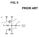
- FIG. 5 is a circuit diagram showing an ESD protection circuit for an input terminal of a conventional semiconductor device.
- the resistors 92 and 93 serially connected to the input terminal 91 slow down the propagation of a surge from the input terminal 91 to the internal circuit, and prevent the rush current into the internal circuit.
- the PMOS transistor 94 and the NMOS transistor 95 which are normally off, discharge the excess current to the power supply terminal or to the ground terminal respectively through the avalanche breakdown of the PN junction at the drain when the surge invades from the input terminal 91, protecting the internal circuit from the excess current generated by the surge (see, for example, Japanese Published Patent Application H11-121750 ).
- a PMOS transistor or an NMOS transistor having an area large enough to flow a large current caused by the surge has to be arranged for each input terminal between the power supply terminal and input terminal or between the ground terminal and the input terminal, respectively, which sometimes becomes an obstacle in scaling down the IC chip area of the semiconductor device.
- the present invention has been made in view of the above-mentioned problem, and provides a semiconductor device having an ESD protection circuit with a smaller area.
- a semiconductor device including: a P-type semiconductor substrate; an N-type well disposed on the semiconductor substrate and connected to a power supply terminal; a P-type diffusion resistor disposed in the well and having one end connected to an input terminal, a parasitic diode formed between the well and the diffusion resistor; a first NMOS transistor having a gate and a source both connected to a ground terminal and having a drain connected to another end of the diffusion resistor; and a second NMOS transistor disposed between the power supply terminal and the ground terminal, and having a gate connected to the ground terminal; wherein electrons charged in the gate of the first NMOS transistor are pulled out from the input terminal through the second NMOS transistor and the parasitic diode.
- the area of a semiconductor device can be made smaller to the extent that a diode is arranged on the side of the power supply terminal after omitting a conventionally used PMOS transistor in an ESD protection circuit for an input terminal.
- FIG. 1 shows an equivalent circuit for an ESD protection circuit.
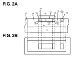
- FIGS. 2A and 2B show a resistor and a parasitically formed diode of FIG. 1 , in which FIG.2A is a schematic sectional view and FIG.2B is a schematic plan view.
- An ESD protection circuit 10 arranged for an input terminal 11 has a P-type diffusion resistor 12, a resistor 13, a diode 14, and an NMOS transistor 15. As shown in FIGS.2A and 2B one end of the P-type diffusion resistor 12 arranged in an N-type well 18 formed on a P-type semiconductor substrate is connected to the input terminal 11. The N-type well 18 is connected to the power supply terminal. In the diode 14 an anode is connected to the diffusion resistor 12 and a cathode is connected to the power supplying terminal. The diode 14 is formed between the N-type well 18 and the P-type diffusion resistor 12 in FIG. 2A and is connected in the reverse direction to the power supply terminal.
- the gate and the source of the NMOS transistor 15 are connected to the ground terminal, the back gate is also connected to the ground terminal, and the drain is connected to the other end of the diffusion resistor 12.
- One end of the resistor 13 is connected to the other end of the diffusion resistor 12 and the other end of the resistor 13 is connected to an internal circuit.
- the diode 14 is not a definite single diode as shown in the equivalent circuit of FIG. 1 since the diode 14 is formed parasitically between the diffusion resistor 12 and the N-type well 18. The important point is that the diode 14 disposed between the power supply terminal and the input terminal is arranged closer to the input terminal than the drain of the NMOS transistor 15.
- the arrangement is necessary to establish a current path 20 through the diode 14 disposed between the input terminal and the power supply terminal and also through the diode 21 whose cathode is connected to the power supplying terminal and whose anode is connected to the ground terminal, and formed in the P-type semiconductor substrate, while the current is stranded by the diffusion resistor 12 and the parasitic capacitance.
- N-type diffusion region 19 is formed in the N-type well 18 which is formed on the surface of the P-type semiconductor substrate 17.
- the N-type diffusion region 19 is connected to the power supplying terminal.
- the diffusion resistor 12 formed of a P-type low-concentration diffusion region 12c and P-type high-concentration diffusion regions 12a and 12b is arranged in the N-type well 18.
- An input terminal 11 is connected to the diffusion region 12a which is one end of the diffusion resistor 12.
- the N-type diffusion region 19 for providing a contact to the N-type well 18 is only arranged in the vicinity of the diffusion region 12b which is the other end of the diffusion resistor 12.
- a test method for a measurement of immunity (strength) against ESD, in which electrons, which have negative charge and have been accumulated and charged in the capacitances of the semiconductor substrate, the gate oxide, and the like in the semiconductor device, are pulled out (or filled in as a sense of current direction) all at once from a selected terminal is called a CDM (Charged device Model) test. If the diode 14 is absent in this test, current flows into a substrate region of the NMOS transistor 15, and momentarily generates a voltage difference between the gate electrode and the substrate, leading to a possible destruction of the NMOS transistor.
- CDM Charge device Model
- the reason for the generation of the voltage difference is thought to be that the absence of the path 20 beginning from the input terminal to the ground terminal through the diode 14, the power supply terminal, and the diode 21, through which the electrons accumulated in the gate of the NMOS transistor 15 is pulled out, generates the voltage difference between the gate electrode and the substrate both of which should have essentially the same voltage. It should be noted that the reverse current flows through the diode 21, not the forward current. As shown above the presence of the path 20 between the input terminal and the ground terminal is essential, and the diode 14 and the diode 21 play an indispensable role.
- Resistors 12 and 13 slow down the propagation of a surge from the input terminal 11 to the internal circuit, and prevent the rush current into the internal circuit.
- the N-type diffusion region 19 can be formed to surround the diffusion region 12.
- the diode 14 can be a non-parasitic origin instead of a parasitic diode generated in the diffusion resistor 12, and can be arranged on an input path closer to the input terminal 11 than the resistor 12.
- FIG. 4 shows an equivalent circuit for the second embodiment which differs from the first embodiment at the point where a protection device between the power supplying terminal and the ground terminal is an NMOS transistor 22,whose gate is grounded to turn off, and which is formed on the P-type semiconductor substrate. Since the NMOS transistor 22 has the gate which is connected to the ground, the breakdown voltage thereof can be made lower than that of the diode constructed from the same impurity concentrations.
- the operation of the protection circuit is similar to that of the first embodiment; the breakdown of the junction between the drain and the semiconductor substrate activates the formation of the current path 20.
- Fig. 6 shows an equivalent circuit for the third embodiment.
- Basic configuration is almost the same as that of the first embodiment. The difference is a specific illustration of the construction of the internal circuit connected to the resistor 13.
- the internal circuit illustrated in FIG. 6 includes a typical inverter circuit 25 in which the drain of the NMOS transistor 23 and the drain of the PMOS transistor 24 are mutually connected.
- the inverter circuit 25 the common gate terminal 30 is connected to the input terminal via the resistor 13.
- the configuration shown in the third embodiment has a weak immunity (strength) in the CDM test.
- the benefit of the present invention can be more effectively shown in this configuration. The reason is that the discharge route is limited to the NMOS transistor 15.
- the configuration in which the diffusion resistance 12 and the parasitic diode 14 are implemented completes a discharge route 29, resulting in the separated discharge through the discharge routes 28 and 29. Accordingly another discharge route other than the route through the NMOS transistor 15 can be secured and the ESD immunity (strength) under the CDM test can also be increased.
- protection diodes 26 and 27 As a conventional protection measure for the CDM test, it is well known to have protection diodes 26 and 27, a PMOS transistor whose gate is connected to the power supply terminal and an NMOS transistor whose gate is connected to the ground terminal, on the input terminal as shown in Fig. 6 .
- the insertion of the protection diodes suppresses the occurrence of the voltage difference between the gate and the substrate, increasing the immunity against the CDM test.
- the protection caused by the conventional measure only covers the gate portion of the NMOS transistor and the PMOS transistor constructing the inverter circuit 25. Since the presence of the resistor 13 disables the protection of the NMOS transistor 15 through the protection diodes 26 and 27, the present embodiment gives a greater benefit.
Landscapes
- Semiconductor Integrated Circuits (AREA)
- Metal-Oxide And Bipolar Metal-Oxide Semiconductor Integrated Circuits (AREA)
Abstract
An ESD protection circuit having a smaller area is provided. The ESD protection circuit includes: a P-type diffusion resistor 12 whose one end is connected to an input terminal 11 formed in the N-type well; a diode 14 disposed between the diffusion resistor 12 and the N-type well connected to the power supply terminal; an NMOS transistor 15 whose drain is connected to the other end of the diffusion resistor 12; and a parasitic diode formed between the power supply terminal and the ground terminal.
Description
- The present invention relates to a semiconductor device, in particular, to an ESD protection circuit for protecting an input terminal of a semiconductor device.
- An example for an ESD protection circuit of a conventional semiconductor device is given and explained.
FIG. 5 is a circuit diagram showing an ESD protection circuit for an input terminal of a conventional semiconductor device. - The
resistors input terminal 91 slow down the propagation of a surge from theinput terminal 91 to the internal circuit, and prevent the rush current into the internal circuit. ThePMOS transistor 94 and theNMOS transistor 95, which are normally off, discharge the excess current to the power supply terminal or to the ground terminal respectively through the avalanche breakdown of the PN junction at the drain when the surge invades from theinput terminal 91, protecting the internal circuit from the excess current generated by the surge (see, for example, Japanese Published Patent ApplicationH11-121750 - In the conventional protection circuit a PMOS transistor or an NMOS transistor having an area large enough to flow a large current caused by the surge has to be arranged for each input terminal between the power supply terminal and input terminal or between the ground terminal and the input terminal, respectively, which sometimes becomes an obstacle in scaling down the IC chip area of the semiconductor device.
- The present invention has been made in view of the above-mentioned problem, and provides a semiconductor device having an ESD protection circuit with a smaller area.
- In order to solve the above-mentioned problem, according to one embodiment of the present invention, there is provided a semiconductor device including: a P-type semiconductor substrate; an N-type well disposed on the semiconductor substrate and connected to a power supply terminal; a P-type diffusion resistor disposed in the well and having one end connected to an input terminal, a parasitic diode formed between the well and the diffusion resistor; a first NMOS transistor having a gate and a source both connected to a ground terminal and having a drain connected to another end of the diffusion resistor; and a second NMOS transistor disposed between the power supply terminal and the ground terminal, and having a gate connected to the ground terminal; wherein electrons charged in the gate of the first NMOS transistor are pulled out from the input terminal through the second NMOS transistor and the parasitic diode.
- According to the present invention, the area of a semiconductor device can be made smaller to the extent that a diode is arranged on the side of the power supply terminal after omitting a conventionally used PMOS transistor in an ESD protection circuit for an input terminal.
- Embodiments of the present invention will now be described by way of further example only and with reference to the accompanying drawings, in which:
-
FIG. 1 is a circuit diagram showing a semiconductor device having an ESD protection circuit; -
FIG. 2A is a schematic sectional view of a resistor and a parasitic diode; -
FIG.2B is a schematic plan view of a resistor and a parasitic diode; -
FIG. 3A is a schematic sectional view of another resistor and another parasitic diode; -
FIG.3B is a schematic plan view of another resistor and another parasitic diode; -
FIG. 4 is a circuit diagram showing a semiconductor device having another ESD protection circuit; -
FIG. 5 is a circuit diagram showing a conventional ESD protection circuit; and -
FIG. 6 is a circuit diagram showing a semiconductor device having still another ESD protection circuit. - Now, embodiments of the present invention are described with reference to the accompanying drawings.
- First, a structure of an ESD circuit for an input terminal is explained.
FIG. 1 shows an equivalent circuit for an ESD protection circuit.FIGS. 2A and 2B show a resistor and a parasitically formed diode ofFIG. 1 , in whichFIG.2A is a schematic sectional view andFIG.2B is a schematic plan view. - An
ESD protection circuit 10 arranged for aninput terminal 11 has a P-type diffusion resistor 12, aresistor 13, adiode 14, and anNMOS transistor 15. As shown inFIGS.2A and 2B one end of the P-type diffusion resistor 12 arranged in an N-type well 18 formed on a P-type semiconductor substrate is connected to theinput terminal 11. The N-type well 18 is connected to the power supply terminal. In thediode 14 an anode is connected to thediffusion resistor 12 and a cathode is connected to the power supplying terminal. Thediode 14 is formed between the N-type well 18 and the P-type diffusion resistor 12 inFIG. 2A and is connected in the reverse direction to the power supply terminal. - The gate and the source of the
NMOS transistor 15 are connected to the ground terminal, the back gate is also connected to the ground terminal, and the drain is connected to the other end of thediffusion resistor 12. One end of theresistor 13 is connected to the other end of thediffusion resistor 12 and the other end of theresistor 13 is connected to an internal circuit. Here thediode 14 is not a definite single diode as shown in the equivalent circuit ofFIG. 1 since thediode 14 is formed parasitically between thediffusion resistor 12 and the N-type well 18. The important point is that thediode 14 disposed between the power supply terminal and the input terminal is arranged closer to the input terminal than the drain of theNMOS transistor 15. The arrangement is necessary to establish acurrent path 20 through thediode 14 disposed between the input terminal and the power supply terminal and also through thediode 21 whose cathode is connected to the power supplying terminal and whose anode is connected to the ground terminal, and formed in the P-type semiconductor substrate, while the current is stranded by thediffusion resistor 12 and the parasitic capacitance. - An N-
type diffusion region 19 is formed in the N-type well 18 which is formed on the surface of the P-type semiconductor substrate 17. The N-type diffusion region 19 is connected to the power supplying terminal. Thediffusion resistor 12 formed of a P-type low-concentration diffusion region 12c and P-type high-concentration diffusion regions type well 18. Aninput terminal 11 is connected to thediffusion region 12a which is one end of thediffusion resistor 12. In this embodiment the N-type diffusion region 19 for providing a contact to the N-type well 18 is only arranged in the vicinity of thediffusion region 12b which is the other end of thediffusion resistor 12. - Next, an explanation is given to an characteristic operation for ESD protection in this circuit.
- A test method for a measurement of immunity (strength) against ESD, in which electrons, which have negative charge and have been accumulated and charged in the capacitances of the semiconductor substrate, the gate oxide, and the like in the semiconductor device, are pulled out (or filled in as a sense of current direction) all at once from a selected terminal is called a CDM (Charged device Model) test. If the
diode 14 is absent in this test, current flows into a substrate region of theNMOS transistor 15, and momentarily generates a voltage difference between the gate electrode and the substrate, leading to a possible destruction of the NMOS transistor. The reason for the generation of the voltage difference is thought to be that the absence of thepath 20 beginning from the input terminal to the ground terminal through thediode 14, the power supply terminal, and thediode 21, through which the electrons accumulated in the gate of theNMOS transistor 15 is pulled out, generates the voltage difference between the gate electrode and the substrate both of which should have essentially the same voltage. It should be noted that the reverse current flows through thediode 21, not the forward current. As shown above the presence of thepath 20 between the input terminal and the ground terminal is essential, and thediode 14 and thediode 21 play an indispensable role. -
Resistors input terminal 11 to the internal circuit, and prevent the rush current into the internal circuit. Thediode 14 and theNMOS transistor 15, which are normally off, discharge the charges accumulated in the semiconductor substrate and the gate to the input terminal by the avalanche breakdown of the PN junction at the drain of theNMOS transistor 15 and by the construction of thepath 20 through thediode 14, protecting the internal circuit from the excess current generated by the surge. - As shown in
FIG. 3 the N-type diffusion region 19 can be formed to surround thediffusion region 12. - The
diode 14 can be a non-parasitic origin instead of a parasitic diode generated in thediffusion resistor 12, and can be arranged on an input path closer to theinput terminal 11 than theresistor 12. -
FIG. 4 shows an equivalent circuit for the second embodiment which differs from the first embodiment at the point where a protection device between the power supplying terminal and the ground terminal is anNMOS transistor 22,whose gate is grounded to turn off, and which is formed on the P-type semiconductor substrate. Since theNMOS transistor 22 has the gate which is connected to the ground, the breakdown voltage thereof can be made lower than that of the diode constructed from the same impurity concentrations. The operation of the protection circuit is similar to that of the first embodiment; the breakdown of the junction between the drain and the semiconductor substrate activates the formation of thecurrent path 20. -
Fig. 6 shows an equivalent circuit for the third embodiment. Basic configuration is almost the same as that of the first embodiment. The difference is a specific illustration of the construction of the internal circuit connected to theresistor 13. - The internal circuit illustrated in
FIG. 6 includes atypical inverter circuit 25 in which the drain of theNMOS transistor 23 and the drain of thePMOS transistor 24 are mutually connected. In theinverter circuit 25 the common gate terminal 30 is connected to the input terminal via theresistor 13. Without thediode 14 the configuration shown in the third embodiment has a weak immunity (strength) in the CDM test. The benefit of the present invention can be more effectively shown in this configuration. The reason is that the discharge route is limited to theNMOS transistor 15. - In the CDM test carried out for the
input terminal 11 charge accumulated in the IC chip is discharged through thedischarge route 28. At a glance there seems to exist another route which reaches to theinput terminal 11 through theprotection diode 27, which is an NMOS transistor whose gate is connected to the ground, and through theresistor 13. This other discharge route, however, is obstructed by theresistor 13, and does not work actually. As explained above all the charges accumulated in the IC chip are collected to thedischarge route 28 through theNMOS transistor 15, generating the voltage difference between the gate and the semiconductor substrate, which leads to a dielectric breakdown. - In the present invention the configuration in which the
diffusion resistance 12 and theparasitic diode 14 are implemented completes adischarge route 29, resulting in the separated discharge through thedischarge routes NMOS transistor 15 can be secured and the ESD immunity (strength) under the CDM test can also be increased. - As a conventional protection measure for the CDM test, it is well known to have
protection diodes Fig. 6 . The insertion of the protection diodes suppresses the occurrence of the voltage difference between the gate and the substrate, increasing the immunity against the CDM test. The protection caused by the conventional measure, however, only covers the gate portion of the NMOS transistor and the PMOS transistor constructing theinverter circuit 25. Since the presence of theresistor 13 disables the protection of theNMOS transistor 15 through theprotection diodes - The foregoing description has been given by way of example only and it will be appreciated by a person skilled in the art that modifications can be made without departing from the scope of the present invention.
Claims (8)
- A semiconductor device having an ESD protection circuit (10), comprising:a P-type semiconductor substrate (17);an N-type well (18) disposed on the P-type semiconductor substrate;a P-type diffusion resistor (12) disposed in the N-type well;a diode (14) formed between the N-type well and the P-type diffusion resistor;a first NMOS transistor (15) and a second NMOS transistor (22) disposed on the P-type semiconductor substrate;a ground terminal disposed on the P-type semiconductor substrate; anda power supply terminal disposed on the N-type well (19);wherein one end (12a) of the P-type diffusion resistor is connected to an input terminal, and another end (12b) of the P-type diffusion resistor is connected to a drain of the first NMOS transistor (15) and further connected to an internal circuit;wherein a gate and a source of the first NMOS transistor (15) are connected to the ground terminal; andwherein a drain of the second NMOS transistor (22) is connected to the power supply terminal, and a gate and a source of the second NMOS transistor are connected to the ground terminal.
- A semiconductor device according to claim 1, wherein:electrons charged in the gate of the first NMOS transistor are pulled out from the input terminal through the second NMOS transistor and the diode.
- A semiconductor device having an ESD protection circuit (10), comprising:a P-type semiconductor substrate (17);an N-type well (18) disposed on the P-type semiconductor substrate;a P-type diffusion resistor (12) disposed in the N-type well;a first diode (14) formed between the N-type well and the P-type diffusion resistor;an NMOS transistor (15) and a second diode (21) disposed on the P-type semiconductor substrate;a ground terminal disposed on the P-type semiconductor substrate; anda power supply terminal disposed on the N-type well(19);wherein one end (12a) of the P-type diffusion resistor is connected to an input terminal, and another end (12b) of the P-type diffusion resistor is connected to a drain of the NMOS transistor (15) and further connected to an internal circuit;wherein a gate and a source of the NMOS transistor (15) are connected to the ground terminal; andwherein a cathode of the second diode (21) is connected to the power supply terminal, and an anode of the second diode is connected to the ground terminal.
- A semiconductor device according to claim 3, wherein:electrons charged in the gate of the NMOS transistor are pulled out from the input terminal through the first diode and the second diode.
- A semiconductor device according to any one of the preceding claims, further comprising:a resistor disposed between the diffusion resistor and the internal circuit, the resistor having one end connected to the other end of the diffusion resistor and having another end connected to the internal circuit.
- A semiconductor device according to any one of the preceding claims, wherein:the power supply terminal comprises an N-type diffusion region (19) disposed only in the vicinity of the other end of the diffusion resistor.
- A semiconductor device according to any one of claims 1 to 5, wherein:the power supply terminal comprises an N-type diffusion region (19) disposed around the diffusion resistor.
- A semiconductor device according to any one of the preceding claims, wherein:the internal circuit has a second input terminal, the second input terminal being a common gate electrode of an inverter circuit.
Applications Claiming Priority (2)
| Application Number | Priority Date | Filing Date | Title |
|---|---|---|---|
| JP2013021626 | 2013-02-06 | ||
| JP2013254351A JP6243720B2 (en) | 2013-02-06 | 2013-12-09 | Semiconductor device provided with ESD protection circuit |
Publications (1)
| Publication Number | Publication Date |
|---|---|
| EP2765606A1 true EP2765606A1 (en) | 2014-08-13 |
Family
ID=50064478
Family Applications (1)
| Application Number | Title | Priority Date | Filing Date |
|---|---|---|---|
| EP20140154140 Withdrawn EP2765606A1 (en) | 2013-02-06 | 2014-02-06 | Semiconductor device having an ESD protection circuit |
Country Status (6)
| Country | Link |
|---|---|
| US (1) | US9142543B2 (en) |
| EP (1) | EP2765606A1 (en) |
| JP (1) | JP6243720B2 (en) |
| KR (1) | KR102099371B1 (en) |
| CN (1) | CN103972230B (en) |
| TW (1) | TWI603455B (en) |
Cited By (1)
| Publication number | Priority date | Publication date | Assignee | Title |
|---|---|---|---|---|
| EP3944316A1 (en) * | 2020-07-21 | 2022-01-26 | Nexperia B.V. | An electrostatic discharge protection semiconductor structure and a method of manufacture |
Families Citing this family (10)
| Publication number | Priority date | Publication date | Assignee | Title |
|---|---|---|---|---|
| US9559640B2 (en) | 2015-02-26 | 2017-01-31 | Qualcomm Incorporated | Electrostatic discharge protection for CMOS amplifier |
| CN106158850B (en) * | 2016-08-26 | 2019-06-11 | 华为技术有限公司 | Electrostatic discharge protection device and multi-power domain integrated circuit |
| US10224426B2 (en) | 2016-12-02 | 2019-03-05 | Vishay-Siliconix | High-electron-mobility transistor devices |
| US10381473B2 (en) | 2016-12-02 | 2019-08-13 | Vishay-Siliconix | High-electron-mobility transistor with buried interconnect |
| JP7007564B2 (en) * | 2017-11-10 | 2022-01-24 | ミツミ電機株式会社 | Semiconductor integrated circuit for regulator |
| TWI778071B (en) * | 2018-06-01 | 2022-09-21 | 聯華電子股份有限公司 | Semiconductor device |
| US10693288B2 (en) * | 2018-06-26 | 2020-06-23 | Vishay SIliconix, LLC | Protection circuits with negative gate swing capability |
| US10833063B2 (en) | 2018-07-25 | 2020-11-10 | Vishay SIliconix, LLC | High electron mobility transistor ESD protection structures |
| CN114600242B (en) * | 2019-11-06 | 2025-08-29 | 株式会社索思未来 | semiconductor integrated circuit devices |
| CN114094557A (en) * | 2021-11-11 | 2022-02-25 | 电子科技大学广东电子信息工程研究院 | ESD protection circuit of input signal port based on diffusion resistance |
Citations (8)
| Publication number | Priority date | Publication date | Assignee | Title |
|---|---|---|---|---|
| JPS62101067A (en) * | 1985-10-28 | 1987-05-11 | Nec Corp | Input protecting device |
| JPH11121750A (en) | 1997-10-09 | 1999-04-30 | Mitsubishi Electric Corp | Semiconductor device |
| US5903184A (en) * | 1995-12-19 | 1999-05-11 | Rohm Co., Ltd. | Semiconductor device having protection circuit |
| US5912494A (en) * | 1996-04-02 | 1999-06-15 | Winbond Electronics Corporation | Internal ESD protection structure with contact diffusion |
| US20030052367A1 (en) * | 2001-09-05 | 2003-03-20 | Shi-Tron Lin | Apparatus and method for improved power bus esd protection |
| US20030197997A1 (en) * | 2001-12-21 | 2003-10-23 | Jiunn-Way Miaw | Electro-static discharge protection device for integrated circuit inputs |
| US6894881B1 (en) * | 2002-02-19 | 2005-05-17 | National Semiconductor Corp | ESD protection methods and devices using additional terminal in the diode structures |
| US20100123984A1 (en) * | 2008-11-14 | 2010-05-20 | Mediatek Inc. | Esd protection circuit and circuitry of ic applying the esd protection circuit |
Family Cites Families (23)
| Publication number | Priority date | Publication date | Assignee | Title |
|---|---|---|---|---|
| JPS5122794A (en) * | 1974-08-17 | 1976-02-23 | Japan Atomic Energy Res Inst | SURARIKEITEIONZENSHOSHAHONYORU HORIOREFUINNO GURAFUTOJUGOHOHO |
| JPS5414173A (en) * | 1977-07-04 | 1979-02-02 | Seiko Epson Corp | Semiconductor device |
| JPH0281468A (en) * | 1988-09-17 | 1990-03-22 | Mitsubishi Electric Corp | Input protective circuit |
| JPH04340761A (en) * | 1991-05-17 | 1992-11-27 | Fujitsu Ltd | Semiconductor integrated circuit |
| US5237395A (en) * | 1991-05-28 | 1993-08-17 | Western Digital Corporation | Power rail ESD protection circuit |
| JP3568971B2 (en) * | 1993-04-13 | 2004-09-22 | シチズン時計株式会社 | Semiconductor device protection circuit |
| JPH0766370A (en) * | 1993-08-31 | 1995-03-10 | Fujitsu Ltd | Semiconductor device |
| JPH11265942A (en) * | 1998-03-18 | 1999-09-28 | Hitachi Ltd | Semiconductor integrated circuit device and method of manufacturing the same |
| US6912109B1 (en) * | 2000-06-26 | 2005-06-28 | Taiwan Semiconductor Manufacturing Co., Ltd. | Power-rail ESD clamp circuits with well-triggered PMOS |
| JP3386042B2 (en) * | 2000-08-02 | 2003-03-10 | 日本電気株式会社 | Semiconductor device |
| JP3773506B2 (en) * | 2003-07-24 | 2006-05-10 | 松下電器産業株式会社 | Semiconductor integrated circuit device |
| GB0606685D0 (en) | 2006-04-03 | 2006-05-10 | Xaar Technology Ltd | Droplet Deposition Apparatus |
| JP2009196122A (en) | 2008-02-19 | 2009-09-03 | Toshiba Tec Corp | Inkjet head, and method for producing the same |
| JP5279290B2 (en) * | 2008-02-19 | 2013-09-04 | セイコーインスツル株式会社 | Semiconductor device |
| JP2010041013A (en) * | 2008-08-08 | 2010-02-18 | Oki Semiconductor Co Ltd | Protection circuit |
| JP5546191B2 (en) * | 2009-09-25 | 2014-07-09 | セイコーインスツル株式会社 | Semiconductor device |
| JP5437773B2 (en) | 2009-10-29 | 2014-03-12 | エスアイアイ・プリンテック株式会社 | Liquid ejecting head, liquid ejecting apparatus, and method of manufacturing liquid ejecting head |
| JP5351714B2 (en) | 2009-11-12 | 2013-11-27 | エスアイアイ・プリンテック株式会社 | Liquid ejecting head, liquid ejecting apparatus, and method of manufacturing liquid ejecting head |
| JP5577082B2 (en) * | 2009-12-08 | 2014-08-20 | ルネサスエレクトロニクス株式会社 | Semiconductor device |
| JP2011181848A (en) * | 2010-03-03 | 2011-09-15 | Sharp Corp | Esd protection circuit and semiconductor device equipped with the same |
| JP5603277B2 (en) * | 2011-03-29 | 2014-10-08 | セイコーインスツル株式会社 | ESD protection circuit for semiconductor integrated circuit |
| JP5827044B2 (en) | 2011-06-28 | 2015-12-02 | エスアイアイ・プリンテック株式会社 | Liquid ejecting head, liquid ejecting apparatus, and method of manufacturing liquid ejecting head |
| JP5905266B2 (en) | 2011-06-28 | 2016-04-20 | エスアイアイ・プリンテック株式会社 | Liquid ejecting head, liquid ejecting apparatus, and method of manufacturing liquid ejecting head |
-
2013
- 2013-12-09 JP JP2013254351A patent/JP6243720B2/en not_active Expired - Fee Related
-
2014
- 2014-01-21 TW TW103102114A patent/TWI603455B/en not_active IP Right Cessation
- 2014-01-29 CN CN201410043051.2A patent/CN103972230B/en not_active Expired - Fee Related
- 2014-02-03 KR KR1020140012147A patent/KR102099371B1/en not_active Expired - Fee Related
- 2014-02-04 US US14/172,217 patent/US9142543B2/en not_active Expired - Fee Related
- 2014-02-06 EP EP20140154140 patent/EP2765606A1/en not_active Withdrawn
Patent Citations (8)
| Publication number | Priority date | Publication date | Assignee | Title |
|---|---|---|---|---|
| JPS62101067A (en) * | 1985-10-28 | 1987-05-11 | Nec Corp | Input protecting device |
| US5903184A (en) * | 1995-12-19 | 1999-05-11 | Rohm Co., Ltd. | Semiconductor device having protection circuit |
| US5912494A (en) * | 1996-04-02 | 1999-06-15 | Winbond Electronics Corporation | Internal ESD protection structure with contact diffusion |
| JPH11121750A (en) | 1997-10-09 | 1999-04-30 | Mitsubishi Electric Corp | Semiconductor device |
| US20030052367A1 (en) * | 2001-09-05 | 2003-03-20 | Shi-Tron Lin | Apparatus and method for improved power bus esd protection |
| US20030197997A1 (en) * | 2001-12-21 | 2003-10-23 | Jiunn-Way Miaw | Electro-static discharge protection device for integrated circuit inputs |
| US6894881B1 (en) * | 2002-02-19 | 2005-05-17 | National Semiconductor Corp | ESD protection methods and devices using additional terminal in the diode structures |
| US20100123984A1 (en) * | 2008-11-14 | 2010-05-20 | Mediatek Inc. | Esd protection circuit and circuitry of ic applying the esd protection circuit |
Cited By (2)
| Publication number | Priority date | Publication date | Assignee | Title |
|---|---|---|---|---|
| EP3944316A1 (en) * | 2020-07-21 | 2022-01-26 | Nexperia B.V. | An electrostatic discharge protection semiconductor structure and a method of manufacture |
| US12191344B2 (en) | 2020-07-21 | 2025-01-07 | Nexperia B.V. | Electrostatic Discharge protection semiconductor structure and a method of manufacture |
Also Published As
| Publication number | Publication date |
|---|---|
| CN103972230A (en) | 2014-08-06 |
| CN103972230B (en) | 2018-05-22 |
| JP2014170919A (en) | 2014-09-18 |
| JP6243720B2 (en) | 2017-12-06 |
| TW201448159A (en) | 2014-12-16 |
| TWI603455B (en) | 2017-10-21 |
| KR20140100425A (en) | 2014-08-14 |
| KR102099371B1 (en) | 2020-04-09 |
| US9142543B2 (en) | 2015-09-22 |
| US20140217511A1 (en) | 2014-08-07 |
Similar Documents
| Publication | Publication Date | Title |
|---|---|---|
| US9142543B2 (en) | Semiconductor device having an ESD protection circuit | |
| KR101975608B1 (en) | Electrostatic discharge high voltage type transistor and electrostatic dscharge protection circuit thereof | |
| US12094970B2 (en) | Electrostatic discharge guard ring with complementary drain extended devices | |
| CN102761109B (en) | Power management circuit and high voltage device therein | |
| US10497696B2 (en) | Electrostatic discharge protection circuit with a bi-directional silicon controlled rectifier (SCR) | |
| US9722019B2 (en) | High voltage integrated circuit device | |
| US20140291765A1 (en) | Esd protection structure and esd protection circuit | |
| CN101834433B (en) | Electrostatic discharge prevention circuit based on complementary SCR (Silicon Controlled Rectifier) | |
| CN101339941A (en) | An electrostatic discharge protection circuit | |
| CN101288177A (en) | Low Capacitance Silicon Controlled Rectifier with Trigger Element | |
| US20150029622A1 (en) | Electrostatic discharge protection | |
| US9991253B2 (en) | Protection element, protection circuit, and semiconductor integrated circuit | |
| JP6398696B2 (en) | Electrostatic protection circuit and semiconductor integrated circuit device | |
| CN102270658A (en) | Low-trigger-voltage and low-parasitic-capacitance silicon controlled structure | |
| US10304820B1 (en) | Electrostatic discharge protection apparatus and applications thereof | |
| KR101488566B1 (en) | Electrostatic Discharge Protection Circuit | |
| US8861151B2 (en) | Overvoltage protection circuit and semiconductor integrated circuit | |
| KR100796426B1 (en) | Semiconductor devices | |
| JP6405986B2 (en) | Electrostatic protection circuit and semiconductor integrated circuit device | |
| US10361186B1 (en) | Suppression of parasitic discharge path in an electrical circuit | |
| JP4763324B2 (en) | Electrostatic protection circuit and semiconductor device including the electrostatic protection circuit | |
| CN104022111B (en) | Electrostatic discharge protective structure with bidirectional protective capacity | |
| US10181466B2 (en) | Electrostatic discharge protection apparatus and applications thereof | |
| TW201332082A (en) | Semiconductor device | |
| CN102097431B (en) | Chip and its electrostatic discharge protection components |
Legal Events
| Date | Code | Title | Description |
|---|---|---|---|
| PUAI | Public reference made under article 153(3) epc to a published international application that has entered the european phase |
Free format text: ORIGINAL CODE: 0009012 |
|
| 17P | Request for examination filed |
Effective date: 20140206 |
|
| AK | Designated contracting states |
Kind code of ref document: A1 Designated state(s): AL AT BE BG CH CY CZ DE DK EE ES FI FR GB GR HR HU IE IS IT LI LT LU LV MC MK MT NL NO PL PT RO RS SE SI SK SM TR |
|
| AX | Request for extension of the european patent |
Extension state: BA ME |
|
| STAA | Information on the status of an ep patent application or granted ep patent |
Free format text: STATUS: THE APPLICATION IS DEEMED TO BE WITHDRAWN |
|
| 18D | Application deemed to be withdrawn |
Effective date: 20150214 |