EP2765472B1 - Boost unit, power conditioner, photovoltaic system, program, and voltage tracking method - Google Patents
Boost unit, power conditioner, photovoltaic system, program, and voltage tracking method Download PDFInfo
- Publication number
- EP2765472B1 EP2765472B1 EP13188780.4A EP13188780A EP2765472B1 EP 2765472 B1 EP2765472 B1 EP 2765472B1 EP 13188780 A EP13188780 A EP 13188780A EP 2765472 B1 EP2765472 B1 EP 2765472B1
- Authority
- EP
- European Patent Office
- Prior art keywords
- boost circuit
- voltage
- boost
- clock time
- circuit
- Prior art date
- Legal status (The legal status is an assumption and is not a legal conclusion. Google has not performed a legal analysis and makes no representation as to the accuracy of the status listed.)
- Active
Links
- 238000000034 method Methods 0.000 title claims description 9
- 230000000875 corresponding effect Effects 0.000 description 22
- 239000003990 capacitor Substances 0.000 description 15
- 239000004065 semiconductor Substances 0.000 description 7
- 230000007423 decrease Effects 0.000 description 3
- 238000010586 diagram Methods 0.000 description 2
- 238000012935 Averaging Methods 0.000 description 1
- 238000004891 communication Methods 0.000 description 1
- 230000001276 controlling effect Effects 0.000 description 1
- 230000002596 correlated effect Effects 0.000 description 1
- 238000009413 insulation Methods 0.000 description 1
- 230000015654 memory Effects 0.000 description 1
- 230000004044 response Effects 0.000 description 1
- 230000002123 temporal effect Effects 0.000 description 1
- 230000001960 triggered effect Effects 0.000 description 1
- 210000003462 vein Anatomy 0.000 description 1
- 238000004804 winding Methods 0.000 description 1
Images

Classifications
-
- H—ELECTRICITY
- H02—GENERATION; CONVERSION OR DISTRIBUTION OF ELECTRIC POWER
- H02J—CIRCUIT ARRANGEMENTS OR SYSTEMS FOR SUPPLYING OR DISTRIBUTING ELECTRIC POWER; SYSTEMS FOR STORING ELECTRIC ENERGY
- H02J3/00—Circuit arrangements for ac mains or ac distribution networks
- H02J3/38—Arrangements for parallely feeding a single network by two or more generators, converters or transformers
- H02J3/381—Dispersed generators
-
- H—ELECTRICITY
- H02—GENERATION; CONVERSION OR DISTRIBUTION OF ELECTRIC POWER
- H02J—CIRCUIT ARRANGEMENTS OR SYSTEMS FOR SUPPLYING OR DISTRIBUTING ELECTRIC POWER; SYSTEMS FOR STORING ELECTRIC ENERGY
- H02J2300/00—Systems for supplying or distributing electric power characterised by decentralized, dispersed, or local generation
- H02J2300/20—The dispersed energy generation being of renewable origin
- H02J2300/22—The renewable source being solar energy
- H02J2300/24—The renewable source being solar energy of photovoltaic origin
- H02J2300/26—The renewable source being solar energy of photovoltaic origin involving maximum power point tracking control for photovoltaic sources
-
- Y—GENERAL TAGGING OF NEW TECHNOLOGICAL DEVELOPMENTS; GENERAL TAGGING OF CROSS-SECTIONAL TECHNOLOGIES SPANNING OVER SEVERAL SECTIONS OF THE IPC; TECHNICAL SUBJECTS COVERED BY FORMER USPC CROSS-REFERENCE ART COLLECTIONS [XRACs] AND DIGESTS
- Y02—TECHNOLOGIES OR APPLICATIONS FOR MITIGATION OR ADAPTATION AGAINST CLIMATE CHANGE
- Y02E—REDUCTION OF GREENHOUSE GAS [GHG] EMISSIONS, RELATED TO ENERGY GENERATION, TRANSMISSION OR DISTRIBUTION
- Y02E10/00—Energy generation through renewable energy sources
- Y02E10/50—Photovoltaic [PV] energy
- Y02E10/56—Power conversion systems, e.g. maximum power point trackers
Definitions
- the present invention relates to a boost unit, a power conditioner, a photovoltaic system, a program, and a voltage tracking method.
- MPPT control Maximum Power Point Tracking control
- At least two photovoltaic strings which are installed on an east side and a west side, respectively, to exert different power characteristics, are occasionally connected in parallel to one boost circuit such as the boost chopper.
- one boost circuit such as the boost chopper.
- the MPPT control triggered based on the temporal derivative of the power exceeding a thershold and comprising all the features of the preamble of claim 1.
- a boost unit includes: a first boost circuit; a voltage tracking unit configured to track an input voltage at the first boost circuit at which output power of the first boost circuit is maximized while changing the input voltage at the first boost circuit; and a voltage identification unit configured to identify, when a change in input power or output power of the first boost circuit satisfies a predetermined condition, the input voltage at the first boost circuit at which the output power of the first boost circuit is maximized at timing corresponding to the condition.
- the voltage tracking unit tracks the input voltage at the first boost circuit at which the output power of the first boost circuit is maximized while changing the input voltage at the first boost circuit with the identified input voltage at the first boost circuit as a start point.
- the voltage identification unit may identify the input voltage at the first boost circuit at which the output power of the first boost circuit is maximized at the timing corresponding to the predetermined condition when the change in input power or output power of the first boost circuit with respect to the clock time or the change in input power or output power of the first boost circuit with respect to the input voltage at the first boost circuit satisfies the condition.
- the voltage identification unit may identify the input voltage at the first boost circuit at which the output power of the first boost circuit is maximized at the timing based on at least one of a first start clock time and a first end clock time when the first start clock time at which the input voltage at the first boost circuit reaches a first reference voltage is earlier than a reference start clock time and when the first end clock time at which the input voltage at the first boost circuit falls below a second reference voltage is later than a reference end clock time.
- the boost unit may further include a second boost circuit.
- the reference start clock time may be fixed based on a second start clock time at which the input voltage at the second boost circuit reaches the frst reference voltage
- the reference end clock time may be fixed based on a second end clock time at which the input voltage at the second boost circuit falls below the second reference voltage.
- the voltage identification unit may identify the input voltage at the first boost circuit at which the output power of the first boost circuit is maximized, when the first start clock time is earlier than the reference start clock time, when the first end clock time is later than the reference end clock time, and when the input power of the first boost circuit is less than the input power of the second boost circuit by a first reference difference at a reference intermediate clock time between the reference start clock time and the reference end clock time.
- the voltage identification unit may identify, when an amount of change in input power of the first boost circuit falls within a predetermined reference range in a first time period, the input voltage at the first boost circuit at which the output power of the first boost circuit is maximized at the timing corresponding to the condition.
- the voltage identification unit may identify, when a difference between the input power of the first boost circuit at a predetermined first clock time and the input power of the first boost circuit at a predetermined second clock time earlier than the first clock time is less than or equal to a second reference difference and when a difference between the input power of the first boost circuit at the first clock time and the input power of the first boost circuit at a third clock time earlier than the first clock time is less than or equal to a third reference difference, the input voltage at the first boost circuit at which the output power of the first boost circuit is maximized at the timing corresponding to the condition.
- the voltage identification unit may identify, when a plurality of the input voltages at the first boost circuit, at which the input power or the output power of the first boost circuit is maximized, are detected by changing the input voltage at the first boost circuit, the input voltage at the first boost circuit at which the output power of the first boost circuit is maximized at the timing corresponding to the clock time at which the plurality of input voltages are detected.
- the voltage identification unit may identify the input voltage at the first boost circuit at which the output power of the first boost circuit is maximized by changing the input voltage at the first boost circuit to a lower-limit input voltage from an upper-limit input voltage at the first boost circuit.
- a power conditioner includes: the boost unit; and an inverter configured to convert a direct current outputted from the first boost circuit into an alternating current.
- a photovoltaic system includes: the power conditioner; and at least one photovoltaic string in which the voltage is boosted by the first boost circuit.
- a program that causes a computer to execute: a step of tracking an input voltage at a first boost circuit while changing the input voltage at the first boost circuit, output power of the first boost circuit being maximized at the input voltage; a step of identifying, when a change to clock time in input power or output power of the first boost circuit or a change to the input voltage of the first boost circuit in input power or output power of the first boost circuit satisfies a predetermined condition, the input voltage at the first boost circuit at which the output power of the first boost circuit is maximized at timing corresponding to the condition; and a step of tracking, when the input voltage at the first boost circuit at which the output power of the first boost circuit is maximized is identified, the input voltage at the first boost circuit at which the output power of the first boost circuit is maximized while changing the input voltage at the first boost circuit with the identified input voltage at the first boost circuit as a start point.
- a voltage tracking method includes: a step of tracking an input voltage at a first boost circuit while changing the input voltage at the first boost circuit, output power of the first boost circuit being maximized at the input voltage; a step of identifying, when a change to clock time in input power or output power of the first boost circuit or a change to the input voltage of the first boost circuit in input power or output power of the first boost circuit satisfies a predetermined condition, the input voltage at the first boost circuit at which the output power of the first boost circuit is maximized at timing corresponding to the condition; and a step of tracking, when the input voltage at the first boost circuit at which the output power of the first boost circuit is maximized is identified, the input voltage at the first boost circuit at which the output power of the first boost circuit is maximized while changing the input voltage at the first boost circuit with the identified input voltage at the first boost circuit as a start point.
- Fig. 1 is a system configuration diagram illustrating an example of an entire configuration of a photovoltaic system of the embodiment.
- the photovoltaic system includes photovoltaic strings 200a, 200b, and 200c and a power conditioner 10.
- Each of the photovoltaic strings 200a, 200b, and 200c includes a plurality of photovoltaic modules connected in series or parallel.
- the photovoltaic strings 200a, 200b, and 200c are examples of the power supply that outputs a DC voltage.
- the photovoltaic strings 200a and 200b are connected in parallel to one another through diodes D2a and D2b.
- the photovoltaic string 200a is installed on a roof on an east side of a building.
- the photovoltaic string 200b is installed on the roof on a west side of the building.
- the photovoltaic string 200c is installed on the roof on a south side of the building.
- the photovoltaic strings 200a, 200b, and 200c may include the identical number of photovoltaic modules having identical specifications.
- the power conditioner 10 boosts the DC voltages outputted from the photovoltaic strings 200a, 200b, and 200c, converts the boosted DC voltages into AC voltages, and outputs the AC voltages onto a side of a system power supply 300.
- the power conditioner 10 includes capacitors C1a and C1b, boost circuits 20a and 20b, a connection unit 30, a capacitor C2, an inverter 40, a coil L2, a capacitor C3, a connected relay 50, a power supply 60, and a control device 100.
- the power conditioner 10 includes the boost circuits 20a and 20b.
- at least one of the boost circuits 20a and 20b may be provided outside the power conditioner 10.
- the boost unit may be constructed by the boost circuit 20a or 20b and another control device, such as a microcomputer, which controls a boost operation of the boost circuit 20a or 20b.
- the boost circuit 20a includes a coil L1 a, a switch Tra, and a diode D1 a.
- the boost circuit 20a is what is called a chopper switching regulator.
- the switch Tra is an Insulated Gate Bipolar Transistor (IGBT).
- IGBT Insulated Gate Bipolar Transistor
- One end of the coil L1a is connected to one end of the capacitor C1a, and the other end of the coil L1a is connected to a collector of the switch Tra.
- the collector of the switch Tra is connected to an anode of the diode D1a, and an emitter of the switch Tra is connected to the other end of the capacitor C1a.
- the coil L1a accumulates energy based on power from the photovoltaic strings 200a and 200b during an on period of the switch Tra, and discharges the energy during an off period of the switch Tra. Therefore, the boost circuit 20a boosts the DC voltages outputted from the photovoltaic strings 200a and 200b.
- the diode D1 a is provided between the switch Tra and the connection unit 30 to rectify the output from the coil L1 a.
- the diode D1 a prevents the boosted DC voltage from flowing onto an input side from an output side of the boost circuit 20a.
- Both ends of the capacitor C1b are electrically connected to the positive electrode terminal and the negative electrode terminal of the photovoltaic string 200c, respectively, and the capacitor C1 b smoothes the DC voltage outputted from the photovoltaic string 200c.
- the boost circuit 20b includes a coil L1b, a switch Trb, and a diode D1b.
- the boost circuit 20b may be what is called a chopper switching regulator.
- the switch Trb is an Insulated Gate Bipolar Transistor (IGBT).
- IGBT Insulated Gate Bipolar Transistor
- One end of the coil L1b is connected to one end of the capacitor C1b, and the other end of the coil L1 a is connected to a collector of the switch Trb.
- the collector of the switch Trb is connected to the anode of the diode D1 b, and the emitter of the switch Trb is connected to the other end of the capacitor C1 b.
- the coil L1b accumulates the energy based on the power from the photovoltaic string 200c during the on period of the switch Trb, and discharges the energy accumulated during the off period of the switch Trb. Therefore, the boost circuit 20b boosts the DC voltage output from the photovoltaic string 200c.
- the diode D1b is provided between the switch Trb and the connection unit 30 to rectify the output from the coil L1b.
- the diode D1 b prevents the boosted DC voltage from flowing onto the
- the boost circuits 20a and 20b are not limited to the above configuration.
- the boost circuits 20a and 20b may be constructed by insulation type boost circuits, such as a half-bridge boost circuit and a full-bridge boost circuit, which have a transformer winding.
- the connection unit 30 connects the output side of the boost circuit 20a and the output side of the boost circuit 20b in parallel to each other.
- the capacitor C2 smoothes the DC voltage outputted from the connection unit 30.
- the inverter 40 includes a switch, and converts the DC voltages outputted from the boost circuits 20a and 20b into the AC voltages by turning on and off the switch.
- the inverter 40 may be constructed by a single-phase full-bridge PWM inverter including four bridge-connected semiconductor switches. In one pair out of the four semiconductor switches, the semiconductor switches are connected in series. In the other pair out of the four semiconductor switches, the semiconductor switches are connected in series. The other pair of semiconductor switches is connected in parallel to the one pair of the semiconductor switches.
- the coil L2 and the capacitor C3 are provided between the inverter 40 and the system power supply 300.
- the coil L2 and the capacitor C3 remove a noise from the AC voltage outputted from the inverter 40.
- the connected relay 50 is provided between the capacitor C3 and the system power supply 300.
- the power conditioner 10 and the system power supply 300 are electrically connected to each other by turning on the connected relay 50, and the power conditioner 10 and the system power supply 300 are electrically disconnected from each other by turning off the connected relay 50.
- the power supply 60 is constructed by a power supply IC chip.
- the power supply 60 is connected to both the ends of the connection unit 30.
- the power supply 60 generates power indicating a predetermined voltage value from the DC voltage taken out from the connection unit 30, and supplies the generated power to the control device 100.
- One of photovoltaic strings 200a, 200b, and 200c outputs the power while the switches Tra and Trb of the boost circuits 20a and 20b are in an off state, and the voltage input to the connection unit 30 through the boost circuit 20a or 20b reaches a reference voltage, thereby starting up the power supply 60.
- the power supply 60 After the start-up, the power supply 60 generates a driving power driving the control device 100 using the voltage input through the connection unit 30, and supplies the driving power to the control device 100.
- the control device 100 controls the switching operations of the boost circuits 20a and 20b and the inverter 40, boosts the DC voltages outputted from the photovoltaic strings 200a, 200b, and 200c, converts the boosted DC voltages into the AC voltages, and outputs the AC voltages onto the side of the system power supply 300.
- the control device 100 When being started up by the driving power from the power supply 60, the control device 100 issues an instruction to the boost circuits 20a and 20b to start the boost operation.
- the boost circuits 20a and 20b continue the boost operation when the voltage input through the photovoltaic string is greater than or equal to a boostable voltage.
- the boost circuits 20a and 20b cannot properly perform the boost operation, but tentatively stops the boost operation.
- the control device 100 periodically issues the instruction to the boost circuits 20a and 20b to start the boost operation until the boost circuits 20a and 20b can continue the boost operation.
- the control device 100 individually changes the input voltages at the boost circuits 20a and 20b by individually changing boost ratios of the boost circuits 20a and 20b, and individually tracks the voltages, which are input to the boost circuits 20a and 20b to maximize the power in the connection unit 30, by the MPPT control.
- the power conditioner 10 also includes voltage sensors 12a, 12b, and 16 and current sensors 14a, 14b, and 18.
- the voltage sensor 12a detects a voltage Vabin corresponding to a potential difference at both ends of a parallel connection portion in which the photovoltaic strings 200a and 200b are connected in parallel.
- the voltage sensor 12b detects a voltage Vcin corresponding to a potential difference at both ends of the photovoltaic string 200c.
- the voltage sensor 16 detects a voltage Vout corresponding to a potential difference at both ends of the connection unit 30.
- the current sensor 14a detects a current labin, which passes on the input side of the boost circuit 20a through the parallel connection portion in which the photovoltaic strings 200a and 200b are connected in parallel.
- the current sensor 14b detects a current Icin, which is outputted from the photovoltaic string 200c and passes on the input side of the boost circuit 20b.
- the current sensor 18 detects current lout, which is outputted from the boost circuits 20a and 20b and passes through the connection unit 30.
- control device 100 controls the boost ratios of the boost circuits 20a and 20b such that the power is obtained from the photovoltaic strings 200a, 200b, and 200c as much as possible.
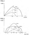
- Fig. 2 illustrates an example of the output power and the output voltages of the photovoltaic strings 200a and 200b in the morning and characteristics of the input power and the input voltages of the boost circuit 20a.
- a dotted line P (200a) illustrates the examples of the characteristics of the output power and the output voltage of the photovoltaic string 200a in the morning.
- An alternate long and short dash line P (200b) illustrates the examples of the characteristics of the output power and the output voltage of the photovoltaic string 200b in the morning.
- a solid line P (200ab) illustrates the example of the characteristics of the input power and the input voltage of the boost circuit 20a.
- the photovoltaic string 200a is installed on the roof on the east side of the building.
- the photovoltaic string 200b is installed on the roof on the west side of the building.
- the output power of one of the photovoltaic strings is less than that of the other photovoltaic string, and two input voltages at the boost circuit 20a emerge (maxima m1 and m2 in Fig. 2 ) at which the power inputted to the boost circuit 20a is maximized.
- the control device 100 controls the boost ratio of the boost circuit 20a to gradually decrease the input voltage at the boost circuit 20a from the voltage corresponding to an open voltage Vo at the photovoltaic string 200a, and searches the input voltage at the boost circuit 20a, at which the input power (the output power) of the boost circuit 20a is maximized, by the MPPT control.
- the control device 100 searches an input voltage Vm1 corresponding to the maximum m1 in Fig. 2 .
- the control device 100 tracks the input voltage, at which the output power of the boost circuit 20a is maximized, by the MPPT control while changing the input voltage at the boost circuit 20a around the input voltage Vm1.
- control device 100 changes the input voltage at the boost circuit 20a around an input voltage Vm2 to be able to maximize the output power of the boost circuit 20a. That is, in the case where at least the two input voltages at the boost circuit 20a at which the power inputted to the boost circuit 20a is maximized emerge, occasionally the control device 100 cannot control the boost ratio of the boost circuit 20a by the MPPT control such that the output power of the boost circuit 20a is maximized.
- control device 100 periodically perform voltage sweep, in which the input voltage at each boost circuit at which the output power of the boost circuit is maximized is identified, by changing the input voltage at the boost circuit to the lower-limit input voltage at which the boost circuit can continue the boost operation from the upper-limit input voltage corresponding to one of the open voltages Vo at the photovoltaic strings connected to the boost circuits.
- the plurality of photovoltaic strings are not necessarily connected in parallel to the boost circuit. Occasionally the photovoltaic string that is provided only on the south side, the east side, or the west side of the building is connected to the boost circuit.
- the boost circuit that is connected to the one photovoltaic string provided only on the south side, the east side, or the west side of the building, probably a plurality of input voltages at the boost circuit, at which the power inputted to the boost circuit is maximized, do not emerge. Accordingly, depending on a condition of the photovoltaic string connected to the boost circuit, the power obtained from the photovoltaic string is not necessarily effectively increased by performing the voltage sweep.
- the control device 100 may estimate which orientation the photovoltaic string connected to each boost circuit is connected based on the change in input power or output power of each boost circuit.
- the control device 100 may estimate which orientation the photovoltaic string connected to each boost circuit is connected based on the change in input power or output power of each boost circuit with respect to a clock time or the change in input power or output power of each boost circuit with respect to the input voltage at the boost circuit.
- the control device 100 may estimate or detect whether the plurality of the input voltages at the boost circuit, at which the input voltage at each boost circuit is maximized, emerge. In a time period having a high probability that the plurality of the maximized input voltages emerge, the control device 100 performs the voltage sweep to the boost circuit having the high probability that the plurality of the input voltages, at which the input power is maximized, emerge.
- the control device 100 may identify the boost circuit to which the voltage sweep should be performed, and identify the time period to which the voltage sweep should be performed to the identified boost circuit. Based on the change in input power or output power of each boost circuit with respect to the clock time or the change in input power or output power of each boost circuit with respect to the input voltage at the boost circuit, the control device 100 may identify the boost circuit to which the voltage sweep should be performed, and identify the time period to which the voltage sweep should be performed to the identified boost circuit. The control device 100 may determine whether the boost circuit, in which the plurality of the input voltages at which the input power is maximized emerge, exist by performing the voltage sweep to each boost circuit during an initial operation.
- the control device 100 identifies the boost circuit, in which the plurality of the input voltages at which the input power is maximized emerge, as the boost circuit to which the voltage sweep should be performed, and the control device 100 may perform the voltage sweep to the identified boost circuit even after the initial operation.
- the operation of the control device 100 may be set at a stage at which the power conditioner is installed such that the voltage sweep is performed to the boost circuits to which the photovoltaic strings installed on the roofs of the east side and the west side are connected in a predetermined time period. Accordingly, in the present embodiment, the control device 100 can effectively perform the voltage sweep. Therefore, a probability that the maximum power is obtained from the photovoltaic string is improved, and the generation of the time period during which the power from the photovoltaic string is not used due to the voltage sweep can be reduced.
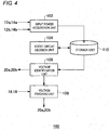
- Fig. 3 is a view illustrating an example of time changes in output power of the photovoltaic strings 200a, 200b, and 200c of the day.
- the dotted line P (200a) indicates the example of the time change in output power of the photovoltaic string 200a installed on the east side of the building.
- the alternate long and short dash line P (200b) indicates the example of the time change in output power of the photovoltaic string 200b installed on the west side of the building.
- the solid line P (200ab) indicates the example of the time change in total output power of the photovoltaic strings 200a and 200b.
- the solid line P (200c) indicates the example of the time change in output power of the photovoltaic string 200c installed on the south side of the building.
- the photovoltaic string 200a Because the photovoltaic string 200a is installed on the east side of the building, the photovoltaic string 200a starts the generation of the output power from a clock time Tsa earlier than a clock time Tsc at which the photovoltaic string 200c installed on the south side of the building starts the generation of the output power. Because the photovoltaic string 200b is installed on the west side of the building, the photovoltaic string 200b ends the generation of the output power from a clock time Tfb later than a clock time Tfc at which the photovoltaic string 200c ends the generation of the output power. That is, the combined power of the photovoltaic strings 200a and 200b is generated from the clock time Tsa earlier than the clock time Tsc, and generated until the clock time Tfb later than the clock time Tfc.
- the combined power of the photovoltaic strings 200a and 200b is less than the output power of photovoltaic string 200c.
- the combined power of the photovoltaic strings 200a and 200b hardly changes between a clock time Tn3 around 2:00 p.m. later than the clock time Tn1 and a clock time Tn2 around 10:00 a.m. earlier than the clock time Tn1.
- the control device 100 may determine whether the voltage sweep is performed to each boost circuit in consideration of the characteristic of the time change in output power of the photovoltaic string.
- Fig. 4 is a view illustrating an example of a functional block of the control device 100.
- the control device 100 may be constructed by a microcomputer.
- the control device 100 includes an input power acquisition unit 102, a boost circuit decision unit 104, a voltage identification unit 106, a voltage tracking unit 108, and a storage unit 110.
- the input power acquisition unit 102 periodically acquires the power inputted to each boost circuit and the input power of the connection unit 30 to which the power is inputted from the boost circuit. For example, the input power acquisition unit 102 acquires the input power every one hour or every 30 minutes and stores the input power in the storage unit 110.
- the input power acquisition unit 102 may acquire power Wab inputted to the boost circuit 20a by multiplying the voltage Vabin detected by the voltage sensor 12a and the current labin detected by the current sensor 14a.
- the input power acquisition unit 102 may acquire power Wc inputted to the boost circuit 20b by multiplying the voltage Vein detected by the voltage sensor 12b and the current Icin detected by the current sensor 14b.
- the input power acquisition unit 102 may acquire power Wout, in which the power outputted from the boost circuits 20a and 20b is combined, by multiplying the voltage Vout detected by the voltage sensor 16 and the current lout detected by the current sensor 18.
- the boost circuit decision unit 104 decides the boost circuit, to which the voltage sweep is performed, based on the change in power inputted to each boost circuit with respect to the clock time.
- the boost circuit decision unit 104 decides the boost circuit, to which the voltage sweep is performed, when the change in power inputted to each boost circuit with respect to the clock time satisfies a predetermined condition.
- the boost circuit decision unit 104 may decide that the boost circuit is the target boost circuit to which the voltage sweep is performed when the boost circuit satisfies a condition A.
- a start clock time Ts at which the input voltage at the boost circuit reaches a reference voltage Vth1 is earlier than a reference start clock time Tsth
- an end clock time Tf at which the input voltage at the boost circuit falls below a reference voltage Vth2 is later than a reference end clock time Tfth.
- the reference voltage Vth1 may be a minimum voltage necessary for the boost circuit to perform the boost operation using the power from the photovoltaic string.
- the reference voltage Vth2 may be a voltage at which the boost circuit becomes unable to perform the boost operation using the power from the photovoltaic string.
- the reference voltage Vth1 and the reference voltage Vth2 may be equal to each other.
- the reference start clock time Tsth may be a clock time at which the voltage at the photovoltaic string installed on the south side of the building reaches the reference voltage Vth1.
- the reference end clock time Tfth may be a clock time at which the voltage at the photovoltaic string installed on the south side of the building falls below the reference voltage Vth2.
- the boost circuit decision unit 104 may decide that the boost circuit satisfying the condition A is the target boost circuit to which the voltage sweep is performed.
- the boost circuit decision unit 104 may decide that the boost circuit is the target boost circuit to which the voltage sweep is performed when the boost circuit satisfies the condition A and a condition B.
- the input power of the boost circuit at a reference intermediate clock time Tmth between the reference start clock time Tsth and the reference end clock time Tfth is less than or equal to the input power of the other boost circuit by a reference difference ⁇ W1.
- the reference intermediate clock time Tmth may be the noon.
- the boost circuit decision unit 104 determines that possibly the combined power of the photovoltaic strings installed on the east and west sides of the building is inputted to the boost circuit, and decides that the boost circuit is the target boost circuit to which the voltage sweep is performed.
- the boost circuit decision unit 104 may decide that the boost circuit is the boost circuit to which the voltage sweep is performed when the boost circuit satisfies a condition C.
- a condition C an amount of change in input power of the boost circuit in a predetermined first time period falls within a predetermined reference range.
- the first time period may be a time period from 10:00 a.m. to 2:00 p.m.
- the boost circuit decision unit 104 may decide that the boost circuit is the boost circuit to which the voltage sweep is performed when the boost circuit satisfies the condition C.
- the boost circuit decision unit 104 may decide that the boost circuit is the boost circuit to which the voltage sweep is performed when the boost circuit satisfies a condition D.
- a difference between the input power of the boost circuit at the predetermined first clock time and the input power of the boost circuit at a second clock time earlier than the first clock time is less than or equal to a reference difference ⁇ W2
- a difference between the input power of the boost circuit at the predetermined first clock time and the input power of the boost circuit at a third clock time earlier than the first clock time is less than or equal to a reference difference ⁇ W3.
- the boost circuit decision unit 104 may decide that the boost circuit is the boost circuit to which the voltage sweep is performed when the boost circuit satisfies the condition D.
- the reference difference ⁇ W2 and the reference difference ⁇ W3 may be equal to each other.
- the boost circuit decision unit 104 may decide that the boost circuit is the boost circuit to which the voltage sweep is performed when the boost circuit satisfies at least two of the conditions A, B, C, and D.
- the boost circuit decision unit 104 may decide that the boost circuit is the boost circuit to which the voltage sweep is performed when the change in input power or output power of the boost circuit with respect to the input voltage at the boost circuit satisfies a predetermined condition. For example, the boost circuit decision unit 104 performs the voltage sweep to each boost circuit in the morning and the late afternoon at predetermined timing, at a time the power conditioner 10 is installed, four times a year, and the like, and determines whether the plural maxima emerge in the power inputted to the boost circuit.
- the boost circuit decision unit 104 may determine that possibly the combined power of the photovoltaic strings installed on the east and west sides of the building is inputted to the boost circuit, and decide that the boost circuit is the target boost circuit to which the voltage sweep is performed.
- the boost circuit decision unit 104 may decide the timing when the voltage sweep is performed based on the start clock time Ts and the end clock time Tf of the boost circuit to which the voltage sweep is performed. For example, the boost circuit decision unit 104 may decide at least one time of the timing between one hour later from the start clock time Ts and one hour before from the end clock time Tf as the timing when the voltage sweep is performed.
- the boost circuit decision unit 104 may identify the time period having the high possibility that the maximum emerges from a result of the voltage sweep performed at the time the power conditioner 10 is installed, four times a year, and the like, and the boost circuit decision unit 104 may decide the identified time period as the timing when the voltage sweep is performed.
- the input power acquisition unit 102 periodically acquires the input power of each boost circuit and stores the input power of each boost circuit in the storage unit 110.
- the boost circuit decision unit 104 may calculate average input power by averaging the input power of each time period acquired by the input power acquisition unit 102 in a predetermined period, for example, one week or two weeks, and decide the boost circuit to which the voltage sweep is performed based on each average input power.
- the boost circuit decision unit 104 stores the boost circuit, to which the boost circuit decision unit 104 decides to perform the voltage sweep based on the condition, and the clock time at which the voltage sweep is performed to the boost circuit in the storage unit 110 while correlating the boost circuit and the clock time to each other.
- the voltage identification unit 106 identifies the input voltage at the boost circuit at which the output power of the boost circuit is maximized at the timing corresponding to the condition.
- the voltage identification unit 106 identifies the input voltage at the boost circuit, at which the input power of the boost circuit is maximized, by performing the voltage sweep to the boost circuit to which the boost circuit decision unit 104 decides to perform the voltage sweep.
- the voltage identification unit 106 gradually decreases the input voltage at the boost circuit to a lower-limit input voltage at which the boost circuit can perform the boost operation from an upper-limit input voltage corresponding to an open voltage at the photovoltaic string connected to the boost circuit by changing the boost ratio of the boost circuit, and the voltage identification unit 106 performs the voltage sweep by searching the input voltage at the boost circuit corresponding to the maximum combined power in the detected combined power Wout of the connection unit 30.
- the voltage tracking unit 108 tracks the input voltage at each boost circuit at which the output power of the boost circuit is maximized while changing the input voltage at the boost circuit.
- the voltage tracking unit 108 may track the input voltage at each boost circuit, at which the output power of the boost circuit is maximized, by the MPPT control.
- the voltage tracking unit 108 individually controls the boost ratios of the boost circuits 20a and 20b by individually controlling the switches Tra and Trb of the boost circuits 20a and 20b, and tracks the input voltages at the boost circuits 20a and 20b at which the output power of the boost circuits 20a and 20b is maximized.
- the voltage tracking unit 108 multiplies the voltage Vout from the voltage sensor 16 and the current lout from the current sensor 18 while changing the boost ratios of the boost circuits 20a and 20b, thereby calculating the combined power Wout of the connection unit 30 as needed basis, and the voltage tracking unit 108 controls the input voltages at the boost circuits 20a and 20b such that the calculated combined power Wout is maximized.
- the voltage tracking unit 108 identifies the input voltage at each boost circuit at which the output power of the boost circuit is maximized at the timing corresponding to the condition.
- the voltage tracking unit 108 tracks the input voltage at the boost circuit at which the output power of the boost circuit is maximized while changing the input voltage at the boost circuit with the input voltage based on the input voltage at the identified boost circuit as the starting point.
- the voltage tracking unit 108 may track the input voltage at the boost circuit at which the output power of the boost circuit is maximized by the MPPT control with the input voltage at the identified boost circuit as the starting point.
- the boost circuit decision unit 104 decides the boost circuit satisfying the condition as the target boost circuit to which the voltage sweep is performed.
- the voltage identification unit 106 periodically performs the voltage sweep to the boost circuit in a predetermined period from the timing corresponding to the predetermined condition, for example, from the start clock time at which the input voltage at the boost circuit satisfying the predetermined condition reaches the reference voltage Vth1.
- the voltage identification unit 106 periodically performs the voltage sweep to the boost circuit from the predetermined time before the end clock time, at which the input voltage at the boost circuit falls below the reference voltage Vth2, until the end clock time.
- the voltage sweep is performed to the boost circuit, in which possibly the plural maxima of the input power of the boost circuit exist with respect to the input voltage at the boost circuit, in the period during which possibly the plural maxima of the input power of the boost circuit exist with respect to the input voltage at the boost circuit.
- the voltage identification unit 106 performs the voltage sweep to the boost circuit having the possibility that the power increases rather than the case that the MPPT control is simply performed. Therefore, a probability that the maximum power is obtained from the photovoltaic string is improved, and the generation of the time period during which the power from the photovoltaic string is not effectively used due to the voltage sweep can be reduced.
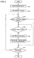
- Fig. 5 is a flowchart illustrating a boost circuit control procedure of the control device 100 when the voltage outputted from one of the photovoltaic strings reaches the reference voltage Vth1.
- the control device 100 When being started up by the driving power from the power supply 60, the control device 100 issues an instruction to the boost circuits 20a and 20b to start the boost operation. In response to the instruction, the boost circuits 20a and 20b turn on and off the switches Tra and Trb to start the boost operation (S100). When the voltage at the photovoltaic string connected to the boost circuit does not reach the reference voltage Vth1, the control device 100 tentatively stops the boost operation, and issues the instruction to the boost circuit to start the boost operation again after a predetermined period elapses.
- the voltage tracking unit 108 performs the MPPT control to the boost circuit to which the boost operation can be performed, and the voltage tracking unit 108 tracks the input voltage at the boost circuit at which the input power of the boost circuit is maximized (S102).
- the voltage tracking unit 108 refers to the storage unit 110 to determine whether the boost circuit that continues the boost operation includes the target boost circuit to which the voltage sweep is performed (S104): For example, the voltage tracking unit 108 determines that the target boost circuit to which the voltage sweep is performed is included when the boost circuit 20a continues the boost operation.
- the voltage identification unit 106 refers to the storage unit 110 to identify the execution timing of the voltage sweep correlated to the target boost circuit. In the case of the execution timing of the voltage sweep, for example, when the present time is included in the specific time period of the morning or the late afternoon, the voltage identification unit 106 performs the voltage sweep to the target boost circuit (S108).
- the voltage identification unit 106 gradually decreases the input voltage at the boost circuit to the lower-limit input voltage at which the boost circuit can perform the boost operation from the upper-limit input voltage corresponding to the open voltage at the photovoltaic string connected to the boost circuit by changing the boost ratio of the boost circuit, and the voltage identification unit 106 searches the input voltage at the boost circuit corresponding to the maximum combined power in the detected combined power Wout of the connection unit 30, and identifies the input voltage at the boost circuit corresponding to the maximum output power.
- the voltage tracking unit 108 performs the MPPT control based on the result of the voltage sweep performed by the voltage identification unit 106 (S110).
- the voltage tracking unit 108 may continue the MPPT control performed to the boost circuit with the input voltage at the boost circuit corresponding to the maximum combined power identified by the voltage identification unit 106 as the starting point.
- control device 100 Unless the boost circuit is stopped, the control device 100 repeatedly performs the pieces of processing from Step S104 to Step S112.
- the voltage identification unit 106 performs the voltage sweep to the boost circuit having the possibility that the power obtained from the photovoltaic string increases only in the time period having the possibility that the power increases rather than the case that the MPPT control is simply performed. Therefore, the probability that the maximum power is obtained from the photovoltaic string is improved, and the generation of the time period during which the power from the photovoltaic string is not effectively used due to the voltage sweep can be reduced.
- Each unit included in the control device 100 of the present embodiment may be constructed by installing a computer-readable program, which is recorded in a recording medium to perform various pieces of processing of tracking an optimum operating point of the boost circuit, and causing the computer to execute the program. That is, the computer acts as each unit included in the control device 100 by causing the computer to execute the program, which performs various pieces of processing of tracking an optimum operating point of the boost circuit, whereby the control device 100 may be constructed.
- the computer includes a CPU, various memories such as a ROM, a RAM, and an EEPROM (registered trademark), a communication bus, and an interface, and the CPU reads and executes sequentially the processing program previously stored in the ROM as firmware, whereby the computer acts as the control device 100.
- various memories such as a ROM, a RAM, and an EEPROM (registered trademark)
- a communication bus and an interface
- the CPU reads and executes sequentially the processing program previously stored in the ROM as firmware, whereby the computer acts as the control device 100.
Landscapes
- Engineering & Computer Science (AREA)
- Power Engineering (AREA)
- Control Of Electrical Variables (AREA)
- Supply And Distribution Of Alternating Current (AREA)
- Direct Current Feeding And Distribution (AREA)
Applications Claiming Priority (1)
| Application Number | Priority Date | Filing Date | Title |
|---|---|---|---|
| JP2013023197A JP6064642B2 (ja) | 2013-02-08 | 2013-02-08 | 昇圧ユニット、パワーコンディショナ、太陽電池システム、プログラム、および電圧追従方法 |
Publications (2)
| Publication Number | Publication Date |
|---|---|
| EP2765472A1 EP2765472A1 (en) | 2014-08-13 |
| EP2765472B1 true EP2765472B1 (en) | 2016-08-24 |
Family
ID=49356309
Family Applications (1)
| Application Number | Title | Priority Date | Filing Date |
|---|---|---|---|
| EP13188780.4A Active EP2765472B1 (en) | 2013-02-08 | 2013-10-15 | Boost unit, power conditioner, photovoltaic system, program, and voltage tracking method |
Country Status (2)
| Country | Link |
|---|---|
| EP (1) | EP2765472B1 (ja) |
| JP (1) | JP6064642B2 (ja) |
Families Citing this family (4)
| Publication number | Priority date | Publication date | Assignee | Title |
|---|---|---|---|---|
| CN106611961B (zh) * | 2015-10-27 | 2019-01-08 | 上海交通大学 | 具有惯性环节的链式级联全域自同步太阳能光伏发电控制装置及方法 |
| CN105938381B (zh) * | 2016-06-02 | 2017-05-10 | 华中科技大学 | 一种基于模糊概率的光伏电池的最大功率点的跟踪方法 |
| WO2019044403A1 (ja) * | 2017-08-31 | 2019-03-07 | 株式会社村田製作所 | 太陽光発電システム、パワーコンディショナ |
| CN110719038B (zh) * | 2019-09-09 | 2021-02-12 | 华为数字技术(苏州)有限公司 | 组串式逆变器的控制方法、装置、系统及存储介质 |
Family Cites Families (5)
| Publication number | Priority date | Publication date | Assignee | Title |
|---|---|---|---|---|
| JP2003134667A (ja) | 2001-10-17 | 2003-05-09 | Mitsubishi Heavy Ind Ltd | 太陽光発電装置 |
| TW201034354A (en) * | 2008-12-20 | 2010-09-16 | Azuray Technologies Inc | Energy conversion systems with power control |
| EP2390751B1 (en) * | 2010-05-28 | 2013-09-04 | Nxp B.V. | Maximum power point tracking method, photovoltaic system controller and photovoltaic system |
| DE102010036966B4 (de) * | 2010-08-12 | 2013-02-28 | Sma Solar Technology Ag | Verfahren zum Betreiben eines Photovoltaikgenerators an einem Arbeitspunkt maximaler Leistung |
| JP2012114380A (ja) * | 2010-11-26 | 2012-06-14 | Kyocera Corp | 制御装置 |
-
2013
- 2013-02-08 JP JP2013023197A patent/JP6064642B2/ja active Active
- 2013-10-15 EP EP13188780.4A patent/EP2765472B1/en active Active
Also Published As
| Publication number | Publication date |
|---|---|
| EP2765472A1 (en) | 2014-08-13 |
| JP2014155332A (ja) | 2014-08-25 |
| JP6064642B2 (ja) | 2017-01-25 |
Similar Documents
| Publication | Publication Date | Title |
|---|---|---|
| US11728724B2 (en) | Bypass circuit and method to bypass power modules in power system | |
| US9583645B2 (en) | Photovoltaic system | |
| US11876369B2 (en) | System and method for interconnected elements of a power system | |
| EP2760118B1 (en) | Power conditioner, photovoltaic system, and abnormality determination method | |
| EP2765472B1 (en) | Boost unit, power conditioner, photovoltaic system, program, and voltage tracking method | |
| EP2768132B1 (en) | Power conditioner, photovoltaic system, and abnormality determination method | |
| US9698710B2 (en) | Solar energy utilization system | |
| EP2779250A2 (en) | Photovoltaic bypass and output switching | |
| CN108200668B (zh) | 电加热器的控制方法、装置、存储介质和处理器 | |
| EP3823152A1 (en) | Power conversion system, conversion circuit control method and program | |
| US20140368058A1 (en) | Photovoltaic bypass and output switching | |
| US20230369965A1 (en) | Bypass Circuit and Method to Bypass Power Modules in Power System | |
| EP2778824A2 (en) | Power conditioner and program | |
| WO2017163690A1 (ja) | 電力変換システム、電力変換装置 | |
| JP6078914B2 (ja) | 太陽電池ストリングの電圧調整回路 | |
| JP6755623B2 (ja) | Pvパワーコンディショナ | |
| CN111149275A (zh) | 蓄电装置 | |
| JP2014183603A (ja) | 電力変換システム | |
| JP2024050377A (ja) | 車載ソーラパネル用の電力制御装置 |
Legal Events
| Date | Code | Title | Description |
|---|---|---|---|
| PUAI | Public reference made under article 153(3) epc to a published international application that has entered the european phase |
Free format text: ORIGINAL CODE: 0009012 |
|
| 17P | Request for examination filed |
Effective date: 20131015 |
|
| AK | Designated contracting states |
Kind code of ref document: A1 Designated state(s): AL AT BE BG CH CY CZ DE DK EE ES FI FR GB GR HR HU IE IS IT LI LT LU LV MC MK MT NL NO PL PT RO RS SE SI SK SM TR |
|
| AX | Request for extension of the european patent |
Extension state: BA ME |
|
| R17P | Request for examination filed (corrected) |
Effective date: 20141218 |
|
| RBV | Designated contracting states (corrected) |
Designated state(s): AL AT BE BG CH CY CZ DE DK EE ES FI FR GB GR HR HU IE IS IT LI LT LU LV MC MK MT NL NO PL PT RO RS SE SI SK SM TR |
|
| GRAP | Despatch of communication of intention to grant a patent |
Free format text: ORIGINAL CODE: EPIDOSNIGR1 |
|
| RIC1 | Information provided on ipc code assigned before grant |
Ipc: H02J 3/38 20060101ALI20160202BHEP Ipc: G05F 1/67 20060101AFI20160202BHEP |
|
| INTG | Intention to grant announced |
Effective date: 20160226 |
|
| GRAS | Grant fee paid |
Free format text: ORIGINAL CODE: EPIDOSNIGR3 |
|
| GRAA | (expected) grant |
Free format text: ORIGINAL CODE: 0009210 |
|
| AK | Designated contracting states |
Kind code of ref document: B1 Designated state(s): AL AT BE BG CH CY CZ DE DK EE ES FI FR GB GR HR HU IE IS IT LI LT LU LV MC MK MT NL NO PL PT RO RS SE SI SK SM TR |
|
| REG | Reference to a national code |
Ref country code: GB Ref legal event code: FG4D |
|
| REG | Reference to a national code |
Ref country code: CH Ref legal event code: EP |
|
| REG | Reference to a national code |
Ref country code: AT Ref legal event code: REF Ref document number: 823617 Country of ref document: AT Kind code of ref document: T Effective date: 20160915 |
|
| REG | Reference to a national code |
Ref country code: IE Ref legal event code: FG4D |
|
| REG | Reference to a national code |
Ref country code: DE Ref legal event code: R096 Ref document number: 602013010556 Country of ref document: DE |
|
| REG | Reference to a national code |
Ref country code: LT Ref legal event code: MG4D |
|
| REG | Reference to a national code |
Ref country code: NL Ref legal event code: MP Effective date: 20160824 |
|
| REG | Reference to a national code |
Ref country code: AT Ref legal event code: MK05 Ref document number: 823617 Country of ref document: AT Kind code of ref document: T Effective date: 20160824 |
|
| PG25 | Lapsed in a contracting state [announced via postgrant information from national office to epo] |
Ref country code: IT Free format text: LAPSE BECAUSE OF FAILURE TO SUBMIT A TRANSLATION OF THE DESCRIPTION OR TO PAY THE FEE WITHIN THE PRESCRIBED TIME-LIMIT Effective date: 20160824 Ref country code: HR Free format text: LAPSE BECAUSE OF FAILURE TO SUBMIT A TRANSLATION OF THE DESCRIPTION OR TO PAY THE FEE WITHIN THE PRESCRIBED TIME-LIMIT Effective date: 20160824 Ref country code: FI Free format text: LAPSE BECAUSE OF FAILURE TO SUBMIT A TRANSLATION OF THE DESCRIPTION OR TO PAY THE FEE WITHIN THE PRESCRIBED TIME-LIMIT Effective date: 20160824 Ref country code: RS Free format text: LAPSE BECAUSE OF FAILURE TO SUBMIT A TRANSLATION OF THE DESCRIPTION OR TO PAY THE FEE WITHIN THE PRESCRIBED TIME-LIMIT Effective date: 20160824 Ref country code: NO Free format text: LAPSE BECAUSE OF FAILURE TO SUBMIT A TRANSLATION OF THE DESCRIPTION OR TO PAY THE FEE WITHIN THE PRESCRIBED TIME-LIMIT Effective date: 20161124 Ref country code: LT Free format text: LAPSE BECAUSE OF FAILURE TO SUBMIT A TRANSLATION OF THE DESCRIPTION OR TO PAY THE FEE WITHIN THE PRESCRIBED TIME-LIMIT Effective date: 20160824 Ref country code: NL Free format text: LAPSE BECAUSE OF FAILURE TO SUBMIT A TRANSLATION OF THE DESCRIPTION OR TO PAY THE FEE WITHIN THE PRESCRIBED TIME-LIMIT Effective date: 20160824 |
|
| PG25 | Lapsed in a contracting state [announced via postgrant information from national office to epo] |
Ref country code: GR Free format text: LAPSE BECAUSE OF FAILURE TO SUBMIT A TRANSLATION OF THE DESCRIPTION OR TO PAY THE FEE WITHIN THE PRESCRIBED TIME-LIMIT Effective date: 20161125 Ref country code: SE Free format text: LAPSE BECAUSE OF FAILURE TO SUBMIT A TRANSLATION OF THE DESCRIPTION OR TO PAY THE FEE WITHIN THE PRESCRIBED TIME-LIMIT Effective date: 20160824 Ref country code: BE Free format text: LAPSE BECAUSE OF NON-PAYMENT OF DUE FEES Effective date: 20161031 Ref country code: AT Free format text: LAPSE BECAUSE OF FAILURE TO SUBMIT A TRANSLATION OF THE DESCRIPTION OR TO PAY THE FEE WITHIN THE PRESCRIBED TIME-LIMIT Effective date: 20160824 Ref country code: ES Free format text: LAPSE BECAUSE OF FAILURE TO SUBMIT A TRANSLATION OF THE DESCRIPTION OR TO PAY THE FEE WITHIN THE PRESCRIBED TIME-LIMIT Effective date: 20160824 Ref country code: LV Free format text: LAPSE BECAUSE OF FAILURE TO SUBMIT A TRANSLATION OF THE DESCRIPTION OR TO PAY THE FEE WITHIN THE PRESCRIBED TIME-LIMIT Effective date: 20160824 Ref country code: PT Free format text: LAPSE BECAUSE OF FAILURE TO SUBMIT A TRANSLATION OF THE DESCRIPTION OR TO PAY THE FEE WITHIN THE PRESCRIBED TIME-LIMIT Effective date: 20161226 |
|
| PG25 | Lapsed in a contracting state [announced via postgrant information from national office to epo] |
Ref country code: EE Free format text: LAPSE BECAUSE OF FAILURE TO SUBMIT A TRANSLATION OF THE DESCRIPTION OR TO PAY THE FEE WITHIN THE PRESCRIBED TIME-LIMIT Effective date: 20160824 Ref country code: RO Free format text: LAPSE BECAUSE OF FAILURE TO SUBMIT A TRANSLATION OF THE DESCRIPTION OR TO PAY THE FEE WITHIN THE PRESCRIBED TIME-LIMIT Effective date: 20160824 |
|
| REG | Reference to a national code |
Ref country code: DE Ref legal event code: R097 Ref document number: 602013010556 Country of ref document: DE |
|
| PG25 | Lapsed in a contracting state [announced via postgrant information from national office to epo] |
Ref country code: BG Free format text: LAPSE BECAUSE OF FAILURE TO SUBMIT A TRANSLATION OF THE DESCRIPTION OR TO PAY THE FEE WITHIN THE PRESCRIBED TIME-LIMIT Effective date: 20161124 Ref country code: PL Free format text: LAPSE BECAUSE OF FAILURE TO SUBMIT A TRANSLATION OF THE DESCRIPTION OR TO PAY THE FEE WITHIN THE PRESCRIBED TIME-LIMIT Effective date: 20160824 Ref country code: CZ Free format text: LAPSE BECAUSE OF FAILURE TO SUBMIT A TRANSLATION OF THE DESCRIPTION OR TO PAY THE FEE WITHIN THE PRESCRIBED TIME-LIMIT Effective date: 20160824 Ref country code: SM Free format text: LAPSE BECAUSE OF FAILURE TO SUBMIT A TRANSLATION OF THE DESCRIPTION OR TO PAY THE FEE WITHIN THE PRESCRIBED TIME-LIMIT Effective date: 20160824 Ref country code: BE Free format text: LAPSE BECAUSE OF FAILURE TO SUBMIT A TRANSLATION OF THE DESCRIPTION OR TO PAY THE FEE WITHIN THE PRESCRIBED TIME-LIMIT Effective date: 20160824 Ref country code: SK Free format text: LAPSE BECAUSE OF FAILURE TO SUBMIT A TRANSLATION OF THE DESCRIPTION OR TO PAY THE FEE WITHIN THE PRESCRIBED TIME-LIMIT Effective date: 20160824 Ref country code: DK Free format text: LAPSE BECAUSE OF FAILURE TO SUBMIT A TRANSLATION OF THE DESCRIPTION OR TO PAY THE FEE WITHIN THE PRESCRIBED TIME-LIMIT Effective date: 20160824 |
|
| REG | Reference to a national code |
Ref country code: CH Ref legal event code: PL |
|
| PLBE | No opposition filed within time limit |
Free format text: ORIGINAL CODE: 0009261 |
|
| STAA | Information on the status of an ep patent application or granted ep patent |
Free format text: STATUS: NO OPPOSITION FILED WITHIN TIME LIMIT |
|
| REG | Reference to a national code |
Ref country code: IE Ref legal event code: MM4A |
|
| REG | Reference to a national code |
Ref country code: FR Ref legal event code: ST Effective date: 20170630 |
|
| PG25 | Lapsed in a contracting state [announced via postgrant information from national office to epo] |
Ref country code: CH Free format text: LAPSE BECAUSE OF NON-PAYMENT OF DUE FEES Effective date: 20161031 Ref country code: LI Free format text: LAPSE BECAUSE OF NON-PAYMENT OF DUE FEES Effective date: 20161031 Ref country code: FR Free format text: LAPSE BECAUSE OF NON-PAYMENT OF DUE FEES Effective date: 20161102 |
|
| 26N | No opposition filed |
Effective date: 20170526 |
|
| PG25 | Lapsed in a contracting state [announced via postgrant information from national office to epo] |
Ref country code: SI Free format text: LAPSE BECAUSE OF FAILURE TO SUBMIT A TRANSLATION OF THE DESCRIPTION OR TO PAY THE FEE WITHIN THE PRESCRIBED TIME-LIMIT Effective date: 20160824 Ref country code: LU Free format text: LAPSE BECAUSE OF NON-PAYMENT OF DUE FEES Effective date: 20161015 |
|
| PG25 | Lapsed in a contracting state [announced via postgrant information from national office to epo] |
Ref country code: IE Free format text: LAPSE BECAUSE OF NON-PAYMENT OF DUE FEES Effective date: 20161015 |
|
| PG25 | Lapsed in a contracting state [announced via postgrant information from national office to epo] |
Ref country code: HU Free format text: LAPSE BECAUSE OF FAILURE TO SUBMIT A TRANSLATION OF THE DESCRIPTION OR TO PAY THE FEE WITHIN THE PRESCRIBED TIME-LIMIT; INVALID AB INITIO Effective date: 20131015 |
|
| GBPC | Gb: european patent ceased through non-payment of renewal fee |
Effective date: 20171015 |
|
| PG25 | Lapsed in a contracting state [announced via postgrant information from national office to epo] |
Ref country code: CY Free format text: LAPSE BECAUSE OF FAILURE TO SUBMIT A TRANSLATION OF THE DESCRIPTION OR TO PAY THE FEE WITHIN THE PRESCRIBED TIME-LIMIT Effective date: 20160824 Ref country code: IS Free format text: LAPSE BECAUSE OF FAILURE TO SUBMIT A TRANSLATION OF THE DESCRIPTION OR TO PAY THE FEE WITHIN THE PRESCRIBED TIME-LIMIT Effective date: 20160824 Ref country code: MK Free format text: LAPSE BECAUSE OF FAILURE TO SUBMIT A TRANSLATION OF THE DESCRIPTION OR TO PAY THE FEE WITHIN THE PRESCRIBED TIME-LIMIT Effective date: 20160824 Ref country code: MT Free format text: LAPSE BECAUSE OF NON-PAYMENT OF DUE FEES Effective date: 20161031 Ref country code: MC Free format text: LAPSE BECAUSE OF FAILURE TO SUBMIT A TRANSLATION OF THE DESCRIPTION OR TO PAY THE FEE WITHIN THE PRESCRIBED TIME-LIMIT Effective date: 20160824 |
|
| PG25 | Lapsed in a contracting state [announced via postgrant information from national office to epo] |
Ref country code: GB Free format text: LAPSE BECAUSE OF NON-PAYMENT OF DUE FEES Effective date: 20171015 |
|
| PG25 | Lapsed in a contracting state [announced via postgrant information from national office to epo] |
Ref country code: AL Free format text: LAPSE BECAUSE OF FAILURE TO SUBMIT A TRANSLATION OF THE DESCRIPTION OR TO PAY THE FEE WITHIN THE PRESCRIBED TIME-LIMIT Effective date: 20160824 Ref country code: TR Free format text: LAPSE BECAUSE OF FAILURE TO SUBMIT A TRANSLATION OF THE DESCRIPTION OR TO PAY THE FEE WITHIN THE PRESCRIBED TIME-LIMIT Effective date: 20160824 |
|
| PGFP | Annual fee paid to national office [announced via postgrant information from national office to epo] |
Ref country code: DE Payment date: 20230830 Year of fee payment: 11 |