EP2760118B1 - Power conditioner, photovoltaic system, and abnormality determination method - Google Patents
Power conditioner, photovoltaic system, and abnormality determination method Download PDFInfo
- Publication number
- EP2760118B1 EP2760118B1 EP14152475.1A EP14152475A EP2760118B1 EP 2760118 B1 EP2760118 B1 EP 2760118B1 EP 14152475 A EP14152475 A EP 14152475A EP 2760118 B1 EP2760118 B1 EP 2760118B1
- Authority
- EP
- European Patent Office
- Prior art keywords
- circuit
- voltage
- power supply
- boost circuit
- current value
- Prior art date
- Legal status (The legal status is an assumption and is not a legal conclusion. Google has not performed a legal analysis and makes no representation as to the accuracy of the status listed.)
- Not-in-force
Links
- 230000005856 abnormality Effects 0.000 title claims description 83
- 238000000034 method Methods 0.000 title claims description 18
- 230000002265 prevention Effects 0.000 claims description 6
- 239000003990 capacitor Substances 0.000 description 17
- 238000012986 modification Methods 0.000 description 10
- 230000004048 modification Effects 0.000 description 10
- 238000004804 winding Methods 0.000 description 10
- 238000012545 processing Methods 0.000 description 9
- 239000004065 semiconductor Substances 0.000 description 7
- 238000010586 diagram Methods 0.000 description 4
- 238000004891 communication Methods 0.000 description 3
- 230000007423 decrease Effects 0.000 description 3
- 238000009413 insulation Methods 0.000 description 3
- 238000001514 detection method Methods 0.000 description 2
- 238000007599 discharging Methods 0.000 description 2
- 230000004044 response Effects 0.000 description 2
- 230000002159 abnormal effect Effects 0.000 description 1
- 230000015556 catabolic process Effects 0.000 description 1
- 238000006731 degradation reaction Methods 0.000 description 1
- 230000001419 dependent effect Effects 0.000 description 1
- 239000000446 fuel Substances 0.000 description 1
- 238000009434 installation Methods 0.000 description 1
- 230000015654 memory Effects 0.000 description 1
- 238000012552 review Methods 0.000 description 1
Images


Classifications
-
- H—ELECTRICITY
- H02—GENERATION; CONVERSION OR DISTRIBUTION OF ELECTRIC POWER
- H02M—APPARATUS FOR CONVERSION BETWEEN AC AND AC, BETWEEN AC AND DC, OR BETWEEN DC AND DC, AND FOR USE WITH MAINS OR SIMILAR POWER SUPPLY SYSTEMS; CONVERSION OF DC OR AC INPUT POWER INTO SURGE OUTPUT POWER; CONTROL OR REGULATION THEREOF
- H02M3/00—Conversion of DC power input into DC power output
- H02M3/02—Conversion of DC power input into DC power output without intermediate conversion into AC
- H02M3/04—Conversion of DC power input into DC power output without intermediate conversion into AC by static converters
- H02M3/10—Conversion of DC power input into DC power output without intermediate conversion into AC by static converters using discharge tubes with control electrode or semiconductor devices with control electrode
- H02M3/145—Conversion of DC power input into DC power output without intermediate conversion into AC by static converters using discharge tubes with control electrode or semiconductor devices with control electrode using devices of a triode or transistor type requiring continuous application of a control signal
- H02M3/155—Conversion of DC power input into DC power output without intermediate conversion into AC by static converters using discharge tubes with control electrode or semiconductor devices with control electrode using devices of a triode or transistor type requiring continuous application of a control signal using semiconductor devices only
- H02M3/156—Conversion of DC power input into DC power output without intermediate conversion into AC by static converters using discharge tubes with control electrode or semiconductor devices with control electrode using devices of a triode or transistor type requiring continuous application of a control signal using semiconductor devices only with automatic control of output voltage or current, e.g. switching regulators
- H02M3/158—Conversion of DC power input into DC power output without intermediate conversion into AC by static converters using discharge tubes with control electrode or semiconductor devices with control electrode using devices of a triode or transistor type requiring continuous application of a control signal using semiconductor devices only with automatic control of output voltage or current, e.g. switching regulators including plural semiconductor devices as final control devices for a single load
- H02M3/1584—Conversion of DC power input into DC power output without intermediate conversion into AC by static converters using discharge tubes with control electrode or semiconductor devices with control electrode using devices of a triode or transistor type requiring continuous application of a control signal using semiconductor devices only with automatic control of output voltage or current, e.g. switching regulators including plural semiconductor devices as final control devices for a single load with a plurality of power processing stages connected in parallel
-
- H—ELECTRICITY
- H02—GENERATION; CONVERSION OR DISTRIBUTION OF ELECTRIC POWER
- H02J—CIRCUIT ARRANGEMENTS OR SYSTEMS FOR SUPPLYING OR DISTRIBUTING ELECTRIC POWER; SYSTEMS FOR STORING ELECTRIC ENERGY
- H02J3/00—Circuit arrangements for AC mains or AC distribution networks
- H02J3/38—Arrangements for parallely feeding a single network by two or more generators, converters or transformers
- H02J3/381—Dispersed generators
-
- H—ELECTRICITY
- H02—GENERATION; CONVERSION OR DISTRIBUTION OF ELECTRIC POWER
- H02M—APPARATUS FOR CONVERSION BETWEEN AC AND AC, BETWEEN AC AND DC, OR BETWEEN DC AND DC, AND FOR USE WITH MAINS OR SIMILAR POWER SUPPLY SYSTEMS; CONVERSION OF DC OR AC INPUT POWER INTO SURGE OUTPUT POWER; CONTROL OR REGULATION THEREOF
- H02M3/00—Conversion of DC power input into DC power output
- H02M3/02—Conversion of DC power input into DC power output without intermediate conversion into AC
- H02M3/04—Conversion of DC power input into DC power output without intermediate conversion into AC by static converters
- H02M3/10—Conversion of DC power input into DC power output without intermediate conversion into AC by static converters using discharge tubes with control electrode or semiconductor devices with control electrode
- H02M3/145—Conversion of DC power input into DC power output without intermediate conversion into AC by static converters using discharge tubes with control electrode or semiconductor devices with control electrode using devices of a triode or transistor type requiring continuous application of a control signal
- H02M3/155—Conversion of DC power input into DC power output without intermediate conversion into AC by static converters using discharge tubes with control electrode or semiconductor devices with control electrode using devices of a triode or transistor type requiring continuous application of a control signal using semiconductor devices only
- H02M3/156—Conversion of DC power input into DC power output without intermediate conversion into AC by static converters using discharge tubes with control electrode or semiconductor devices with control electrode using devices of a triode or transistor type requiring continuous application of a control signal using semiconductor devices only with automatic control of output voltage or current, e.g. switching regulators
-
- H—ELECTRICITY
- H02—GENERATION; CONVERSION OR DISTRIBUTION OF ELECTRIC POWER
- H02J—CIRCUIT ARRANGEMENTS OR SYSTEMS FOR SUPPLYING OR DISTRIBUTING ELECTRIC POWER; SYSTEMS FOR STORING ELECTRIC ENERGY
- H02J2300/00—Systems for supplying or distributing electric power characterised by decentralized, dispersed, or local generation
- H02J2300/20—The dispersed energy generation being of renewable origin
- H02J2300/22—The renewable source being solar energy
- H02J2300/24—The renewable source being solar energy of photovoltaic origin
-
- H—ELECTRICITY
- H02—GENERATION; CONVERSION OR DISTRIBUTION OF ELECTRIC POWER
- H02M—APPARATUS FOR CONVERSION BETWEEN AC AND AC, BETWEEN AC AND DC, OR BETWEEN DC AND DC, AND FOR USE WITH MAINS OR SIMILAR POWER SUPPLY SYSTEMS; CONVERSION OF DC OR AC INPUT POWER INTO SURGE OUTPUT POWER; CONTROL OR REGULATION THEREOF
- H02M1/00—Details of apparatus for conversion
- H02M1/0003—Details of control, feedback or regulation circuits
- H02M1/0009—Devices or circuits for detecting current in a converter
-
- H—ELECTRICITY
- H02—GENERATION; CONVERSION OR DISTRIBUTION OF ELECTRIC POWER
- H02M—APPARATUS FOR CONVERSION BETWEEN AC AND AC, BETWEEN AC AND DC, OR BETWEEN DC AND DC, AND FOR USE WITH MAINS OR SIMILAR POWER SUPPLY SYSTEMS; CONVERSION OF DC OR AC INPUT POWER INTO SURGE OUTPUT POWER; CONTROL OR REGULATION THEREOF
- H02M1/00—Details of apparatus for conversion
- H02M1/0067—Converter structures employing plural converter units, other than for parallel operation of the units on a single load
- H02M1/007—Plural converter units in cascade
-
- H—ELECTRICITY
- H02—GENERATION; CONVERSION OR DISTRIBUTION OF ELECTRIC POWER
- H02M—APPARATUS FOR CONVERSION BETWEEN AC AND AC, BETWEEN AC AND DC, OR BETWEEN DC AND DC, AND FOR USE WITH MAINS OR SIMILAR POWER SUPPLY SYSTEMS; CONVERSION OF DC OR AC INPUT POWER INTO SURGE OUTPUT POWER; CONTROL OR REGULATION THEREOF
- H02M7/00—Conversion of AC power input into DC power output; Conversion of DC power input into AC power output
- H02M7/42—Conversion of DC power input into AC power output without possibility of reversal
- H02M7/44—Conversion of DC power input into AC power output without possibility of reversal by static converters
- H02M7/48—Conversion of DC power input into AC power output without possibility of reversal by static converters using discharge tubes with control electrode or semiconductor devices with control electrode
- H02M7/53—Conversion of DC power input into AC power output without possibility of reversal by static converters using discharge tubes with control electrode or semiconductor devices with control electrode using devices of a triode or transistor type requiring continuous application of a control signal
- H02M7/537—Conversion of DC power input into AC power output without possibility of reversal by static converters using discharge tubes with control electrode or semiconductor devices with control electrode using devices of a triode or transistor type requiring continuous application of a control signal using semiconductor devices only, e.g. single switched pulse inverters
- H02M7/5387—Conversion of DC power input into AC power output without possibility of reversal by static converters using discharge tubes with control electrode or semiconductor devices with control electrode using devices of a triode or transistor type requiring continuous application of a control signal using semiconductor devices only, e.g. single switched pulse inverters in a bridge configuration
-
- Y—GENERAL TAGGING OF NEW TECHNOLOGICAL DEVELOPMENTS; GENERAL TAGGING OF CROSS-SECTIONAL TECHNOLOGIES SPANNING OVER SEVERAL SECTIONS OF THE IPC; TECHNICAL SUBJECTS COVERED BY FORMER USPC CROSS-REFERENCE ART COLLECTIONS [XRACs] AND DIGESTS
- Y02—TECHNOLOGIES OR APPLICATIONS FOR MITIGATION OR ADAPTATION AGAINST CLIMATE CHANGE
- Y02E—REDUCTION OF GREENHOUSE GAS [GHG] EMISSIONS, RELATED TO ENERGY GENERATION, TRANSMISSION OR DISTRIBUTION
- Y02E10/00—Energy generation through renewable energy sources
- Y02E10/50—Photovoltaic [PV] energy
- Y02E10/56—Power conversion systems, e.g. maximum power point trackers
Definitions
- the present invention relates to a power conditioner, a photovoltaic system, and an abnormality determination method.
- a short-circuit current value of a power supply such as a photovoltaic cell is used as a parameter to determine whether the power supply has an abnormality.
- a closed circuit of a string in which a plurality of photovoltaic modules are connected in series is formed through a transistor connected in parallel to the string, and the short-circuit current value of the string is detected.
- Document D1 discloses a power conditioner that boosts a direct current outputted from a first power supply and the power conditioner converts the boosted direct current into an alternating current and outputs the converted alternating current to a system power supply.
- the power conditioner comprises a first boost circuit, an inverter, a connection unit configured to connect an output side of the first boost circuit and an input side of the inverter, a controlling of the voltage at the connection unit and the generation of a short-circuit between the output terminals of the first power supply to form a first closed circuit of the first power supply.
- a short-circuit current value acquisition unit is used to acquire a first short-circuit current value passing through the first closed circuit during a period and a buffer capacitor is connected to a DC bus between the first boost circuit and the inverter.
- Document D2 discloses fault detection based on voltage waveform comparison.
- the object of the present invention is to provide a power conditioner and an abnormality determination unit to detect the short-circuit current value of the power supply such as the photovoltaic cell without adding a new circuit such as the transistor.
- This object is solved by a power conditioner of claim 1 and an abnormality determination unit according to claim 12. Further advantageous embodiments and improvements of the present invention are listed in the dependent claims.
- a power conditioner that boosts a direct current outputted from a first power supply, converts boosted direct current into an alternating current, and outputs the converted alternating current to a system power supply.
- the power conditioner includes: a first boost circuit that includes a first switch connected between output terminals of the first power supply and is configured to boost the direct current from the first power supply by turning on and off the first switch; an inverter configured to convert the direct current outputted from the first boost circuit into the alternating current; a connection unit configured to connect an output side of the first boost circuit and an input side of the inverter; a controller configured to turn on the first switch while setting the output side of the first boost circuit to a voltage higher than a voltage on the input side of the first boost circuit by controlling the voltage at the connection unit, and to generate a short-circuit between the output terminals of the first power supply to form a first closed circuit of the first power supply; a short-circuit current value acquisition unit configured to acquire a first short-circuit
- the first boost circuit may further include a first backflow prevention circuit configured to prevent inflow of a current from the output side of the first boost circuit.
- the power conditioner may further include a second boost circuit that includes a second switch connected between output terminals of a second power supply and is configured to boost the direct current from the second power supply by turning on and off the second switch.
- a connection unit connects the output side of the first boost circuit and an output side of the second boost circuit in parallel to each other; and the controller may turn on and off the second switch to control the voltage at the connection unit, and set the output side of the first boost circuit to the voltage higher than the voltage on the input side of the first boost circuit.
- the controller may control the inverter to control the voltage at the connection unit, and set the output side of the first boost circuit to the voltage higher than the voltage on the input side of the first boost circuit, when the controller turns on and off the second switch to control the voltage at the connection unit and cannot set the output side of the first boost circuit to the voltage higher than the voltage on the input side of the first boost circuit.
- the controller may turn on and off the first switch to control the voltage at the connection unit, turn on the second switch while setting the output side of the second boost circuit to the voltage higher than the voltage on the input side of the second boost circuit, and generate the short-circuit between the output terminals of the second power supply to form a second closed circuit of the second power supply
- the short-circuit current value acquisition unit may acquire a second short-circuit current value passing through the second closed circuit during a period, when the controller turns on and off the first switch to control the voltage at the connection unit and turns on the second switch while setting the output side of the second boost circuit to the voltage higher than the voltage on the input side of the second boost circuit
- the power supply abnormality determination unit may determine whether the second power supply has the abnormality based on comparison between the second short-circuit current value and a second reference current value, the second reference current value being previously fixed based on a characteristic of the second power supply.
- the second boost circuit may further include a second backflow prevention circuit configured to prevent inflow of the current from the output side of the second boost circuit.
- the controller may control the inverter to output a power from the system power supply onto the side of the connection unit, and control the voltage at the connection unit to set the output side of the first boost circuit to the voltage higher than the voltage on the input side of the first boost circuit.
- a photovoltaic system includes: a first photovoltaic cell that is the first power supply; and the power conditioner configured to convert the direct current outputted from the first photovoltaic cell into the alternating current and to output the alternating current onto the side of the system power supply.
- a photovoltaic system includes: a first photovoltaic cell that is of the first power supply; a second photovoltaic cell that is of the second power supply connected in parallel to the first photovoltaic cell; and the power conditioner configured to convert the direct currents outputted from the first and second photovoltaic cells into the alternating currents and to output the alternating currents onto the side of the system power supply.
- an abnormality determination method for determining an abnormality of a first power supply connected to a power conditioner, the power conditioner including a first boost circuit that includes the first switch connected between output terminals of the first power supply and is configured to boost the direct current from the first power supply by turning on and off the first switch, an inverter configured to convert the direct current outputted from the first boost circuit into the alternating current, and a connection unit configured to connect an output side of the first boost circuit and an input side of the inverter; the power conditioner boosting the direct current outputted from the first power supply, converting the boosted direct current into an alternating current, and outputting the converted alternating current onto a side of a system power supply, and the abnormality determination method includes: a step of turning on the first switch while setting the output side of the first boost circuit to a voltage higher than a voltage on the input side of the first boost circuit by controlling the voltage at the connection unit, and generating a short-circuit between the output terminals of the first power supply to form
- the power conditioner may further include a second boost circuit that includes a second switch connected between output terminals of a second power supply and is configured to boost the direct current from the second power supply by turning on and off the second switch, the connection unit may connect the output side of the first boost circuit and the output side of the second boost circuit in parallel to each other; and, in the first closed circuit forming step, the second switch may be turned on and off to control the voltage at the connection unit, and the output side of the first boost circuit may be set to the voltage higher than the voltage on the input side of the first boost circuit.
- a second boost circuit that includes a second switch connected between output terminals of a second power supply and is configured to boost the direct current from the second power supply by turning on and off the second switch
- the connection unit may connect the output side of the first boost circuit and the output side of the second boost circuit in parallel to each other; and, in the first closed circuit forming step, the second switch may be turned on and off to control the voltage at the connection unit, and the output side of the first boost circuit may be set to the
- the inverter in the first closed circuit forming step, may be controlled to control the voltage at the connection unit, and the output side of the first boost circuit may be set to the voltage higher than the voltage on the input side of the first boost circuit, when the second switch cannot be turned on and off to control the voltage at the connection unit and when the output side of the first boost circuit cannot be set to the voltage higher than the voltage on the input side of the first boost circuit.
- the abnormality determination method may further include a step of turning on and off the first switch to control the voltage at the connection unit, turning on the second switch while setting the output side of the second boost circuit to the voltage higher than the voltage on the input side of the second boost circuit, and generating the short-circuit between the output terminals of the second power supply to form a second closed circuit of the second power supply; a step of acquiring a second short-circuit current value passing through the second closed circuit in a period, during which the first switch is turned on and off to control the voltage at the connection unit and the second switch is turned on while the output side of the second boost circuit is set to the voltage higher than the voltage on the input side of the second boost circuit, and a step of determining whether the second power supply has the abnormality based on comparison between the second short-circuit current value and a second reference current value, the second reference current value being previously fixed based on a characteristic of the second power supply.
- Fig. 1 is a system configuration diagram illustrating an example of an entire configuration of a photovoltaic system of the embodiment.
- the photovoltaic system includes photovoltaic strings 200a and 200b and a power conditioner 10.
- Each of the photovoltaic strings 200a and 200b includes a plurality of photovoltaic modules connected in series.
- the photovoltaic strings 200a and 200b are examples of the first power supply and the second power supply, each of which outputs a DC voltage.
- the first power supply and the second power supply may be a photovoltaic cell, a photovoltaic module in which the photovoltaic cells are connected in series or parallel, or a power supply such as a fuel cell..
- the power conditioner 10 boosts the DC voltages outputted from the photovoltaic strings 200a and 200b, converts the boosted DC voltages into AC voltages, and outputs the AC voltages onto a side of a system power supply 300.
- the power conditioner 10 includes capacitors C1a and C1b, boost circuits 20a and 20b, a connection unit 30, a capacitor C2, an inverter 40, a coil L2, a capacitor C3, a connected relay 50, a power supply 60, and a control device 100.
- the boost circuit 20a includes a coil L1a, a switch Tra, and a diode Da.
- the boost circuit 20a is called a chopper switching regulator.
- the switch Tra is an example of the first switch connected between the positive electrode terminal and the negative electrode terminal of the photovoltaic string 200a.
- the switch Tra may be an Insulated Gate Bipolar Transistor (IGBT).
- IGBT Insulated Gate Bipolar Transistor
- One end of the coil L1a is connected to one end of the capacitor C1a, and the other end of the coil L1a is connected to a collector of the switch Tra.
- the collector of the switch Tra is connected to an anode of the diode Da, and an emitter of the switch Tra is connected to the other end of the capacitor C1a.
- the coil L1a accumulates energy based on power from the photovoltaic string 200a during an on period of the switch Tra, and discharges the energy accumulated during an off period of the switch Tra.
- the boost circuit 20a boosts the DC voltage outputted from the photovoltaic string 200a.
- the diode Da is provided between the switch Tra and the connection unit 30, and prevents the boosted DC voltage from flowing onto an input side from an output side of the boost circuit 20a.
- the diode Da is an example of the first backflow prevention element.
- the boost circuit 20b includes a coil L1b, a switch Trb, and a diode Db.
- the boost circuit 20b may be what is called a chopper switching regulator.
- the switch Trb is an example of the second switch connected between the positive electrode terminal and the negative electrode terminal of the photovoltaic string 200b.
- the switch Trb may be an Insulated Gate Bipolar Transistor (IGBT).
- IGBT Insulated Gate Bipolar Transistor
- One end of the coil L1b is connected to one end of the capacitor C1b, and the other end of the coil L1a is connected to a collector of the switch Trb.
- the collector of the switch Trb is connected to an anode of the diode Db, and an emitter of the switch Trb is connected to the other end of the capacitor C1b.
- the coil L1b accumulates energy based on the power from the photovoltaic string 200b during the on period of the switch Trb, and discharges the energy accumulated during the off period of the switch Trb.
- the boost circuit 20b boosts the DC voltage outputted from the photovoltaic string 200b.
- the diode Db is provided between the switch Trb and the connection unit 30, and prevents the boosted DC voltage from flowing onto the input side from the output side of the boost circuit 20b.
- the diode Db is an example of the second backflow prevention element.
- the boost circuits 20a and 20b are not limited to the above configuration.
- the boost circuits 20a and 20b may be constructed as a insulation type boost circuits, such as a half-bridge boost circuit and a full-bridge boost circuit, which have a transformer winding including a primary winding and a secondary winding.
- the insulation type boost circuit includes a plurality of switches that are connected between output terminals of the power supply of the photovoltaic string 200a or the photovoltaic string 200b. The plurality of switches are connected in series with the primary winding. By turning on and off the plurality of switches, an exciting current is passed through the primary winding while an induced current is passed through the secondary winding.
- the boost circuit included in the photovoltaic system is the insulation type boost circuit, such as the full-bridge boost circuit, which has the transformer winding, the plurality of switches, which are connected in series with the primary winding and connected between the output terminals of the power supply, act as the first switch or the second switch.
- the insulation type boost circuit such as the full-bridge boost circuit, which has the transformer winding, the plurality of switches, which are connected in series with the primary winding and connected between the output terminals of the power supply, act as the first switch or the second switch.
- the connection unit 30 connects the output side of the boost circuit 20a and the output side of the boost circuit 20b in parallel to each other.
- the capacitor C2 smooths the DC voltage outputted from the connection unit 30.
- the inverter 40 includes a switch, and converts the DC voltages outputted from the boost circuits 20a and 20b into the AC voltages by turning on and off the switch.
- the inverter 40 may be constructed as a single-phase full-bridge PWM inverter including four bridge-connected semiconductor switches. In one pair out of the four semiconductor switches, the semiconductor switches are connected in series. In the other pair out of the four semiconductor switches, the semiconductor switches are connected in series. The other pair of semiconductor switches is connected in parallel to the one pair of semiconductor switches.
- the coil L2 and the capacitor C3 are provided between the inverter 40 and the system power supply 300.
- the coil L2 and the capacitor C3 remove a noise from the AC voltage outputted from the inverter 40.
- the connected relay 50 is provided between the capacitor C3 and the system power supply 300.
- the power conditioner 10 and the system power supply 300 are electrically connected to each other by turning on the connected relay 50, and the power conditioner 10 and the system power supply 300 are electrically disconnected from each other by turning off the connected relay 50.
- the power supply 60 is constructed by a power supply IC chip.
- the power supply 60 is connected to both the ends of the connection unit 30.
- the power supply 60 generates power indicating a predetermined voltage value from the DC voltage taken out from the connection unit 30, and supplies the generated power to the control device 100.
- the control device 100 controls the switching operations of the boost circuits 20a and 20b and the inverter 40, boosts the DC voltages outputted from the photovoltaic strings 200a and 200b, converts the boosted DC voltages into the AC voltages, and outputs the AC voltages onto the side of the system power supply 300.
- the power conditioner 10 also includes voltage sensors 12a and 12b, current sensors 14a and 14b, and a voltage sensor 16.
- the voltage sensor 12a detects a voltage value Vain corresponding to a potential difference at both the ends of the photovoltaic string 200a.
- the voltage sensor 12b detects a voltage value Vbin corresponding to a potential difference at both the ends of the photovoltaic string 200b.
- the current sensor 14a detects a current value lain corresponding to the current outputted from photovoltaic string 200a.
- the current sensor 14b detects a current value Ibin corresponding to the current outputted from photovoltaic string 200b.
- the voltage sensor 16 detects a voltage value Vout corresponding to a potential difference at both the ends of the connection unit 30.
- Fig. 2 is a view illustrating an example of a functional block of the control device 100.
- the control device 100 acts as the short-circuit current detection device.
- the control device 100 includes a switch controller 102, a short-circuit current value acquisition unit 104, a power supply abnormality determination unit 106, a meteorological information acquisition unit 108, a transmitter/receiver 110, a timing decision unit 112, and a storage unit 114.
- the switch controller 102, the short-circuit current value acquisition unit 104, the power supply abnormality determination unit 106, the meteorological information acquisition unit 108, the timing decision unit 112, and the storage unit 114 may be constructed by a microcomputer.
- the transmitter/receiver 110 may be constructed by a wireless antenna.
- the switch controller 102 is an example of the controller.
- the switch controller 102 accumulates the energy based on the power outputted from the photovoltaic string 200a in the coil L1a during the on period of the switch Tra by turning on and off the switch Tra included in the boost circuit 20a, and boosts the voltage at the photovoltaic string 200a using the boost circuit 20a by discharging the energy from the coil L1a during the off period of the switch Tra.
- the switch controller 102 accumulates the energy based on the power outputted from the photovoltaic string 200b in the coil L1b during the on period of the switch Trb by turning on and off the switch Trb included in the boost circuit 20b, and boosts the voltage at the photovoltaic string 200b using the boost circuit 20b by discharging the energy from the coil L1b during the off period of the switch Trb.
- the switch controller 102 When acquiring the first short-circuit current value that is of the short-circuit current value of the photovoltaic string 200a, the switch controller 102 stops the boost operation of the boost circuit 20a to turn on the switch Tra, thereby forming the first closed circuit of the photovoltaic string 200a.
- the switch controller 102 stops the boost operation of the boost circuit 20b to turn on the switch Trb, thereby forming the second closed circuit of the photovoltaic string 200b.
- the short-circuit current value acquisition unit 104 acquires the first short-circuit current value passing through the first closed circuit when the switch Tra is in the on period while the boost operation of the boost circuit 20a is stopped.
- the short-circuit current value acquisition unit 104 acquires the second short-circuit current value passing through the second closed circuit when the switch Trb is in the on period while the boost operation of the boost circuit 20b is stopped.
- the power supply 60 may acquire a driving power, which is of the power used to drive itself, from the connection unit 30.
- a driving power which is of the power used to drive itself
- the connection unit 30 In the case where the voltage on the input side of the boost circuit 20a is less than that on the output side, the current flows partially onto the side of the inverter 40 from the photovoltaic string 200a through the diode Da. Therefore, the voltage at both the ends of the capacitor C2 fluctuates. That is, the voltage at both the ends of the connection unit 30 fluctuates.
- the power supplied to the power supply 60 becomes unstable, and possibly the power is unstably supplied to the control device 100 from the power supply 60. For this reason, preferably the voltage on the output side of the boost circuit 20a is greater than that on the input side.
- the power supply 60 may directly take the power from the system power supply 300, and generate the power supplied to the control device 100 based on the power output from the system power supply 300.
- the switch controller 102 may control the voltage at the connection unit 30 to set the voltage on the output side of the boost circuit 20a higher than the voltage on the input side of the boost circuit 20a.
- the switch controller 102 may control the voltage at the connection unit 30 such that the voltage at the connection unit 30 is greater than or equal to the voltage on the input side of the boost circuit 20a by turning on and off the switch Trb included in the boost circuit 20b.
- the switch controller 102 may turn on the switch Tra while setting the voltage on the output side of the boost circuit 20a higher than the voltage on the input side of the boost circuit 20a, and generate a short-circuit between the output terminals of the photovoltaic string 200a to form the first closed circuit of the photovoltaic string 200a.
- the switch controller 102 may control the voltage at the connection unit 30 to set the voltage on the output side of the boost circuit 20b higher than the voltage on the input side of the boost circuit 20b.
- the switch controller 102 may control the voltage at the connection unit 30 such that the voltage at the connection unit 30 is greater than or equal to the voltage on the input side of the boost circuit 20b by turning on and off the switch Tra included in the boost circuit 20a.
- the switch controller 102 may turn on the switch Trb while setting the voltage on the output side of the boost circuit 20b higher than the voltage on the input side of the boost circuit 20b, and generate the short-circuit between the output terminals of the photovoltaic string 200b to form the second closed circuit of the photovoltaic string 200b.
- the switch controller 102 may control each switch included in the inverter 40, and increase the voltage at the connection unit 30 such that the voltage at the connection unit 30 is greater than or equal to the voltage on the input side of the boost circuit 20b or the voltage on the input side of the boost circuit 20a based on the power from the system power supply 300.
- the switch controller 102 may output the power onto the side of the connection unit 30 from the system power supply 300 by turning on and off each switch included in the inverter 40, and increase the voltage at the connection unit 30 such that the voltage at the connection unit 30 is greater than or equal to the voltage on the input side of the boost circuit 20a.
- the switch controller 102 may output the power onto the side of the connection unit 30 from the system power supply 300 by turning on and off each switch included in the inverter 40, and increase the voltage at the connection unit 30 such that the voltage at the connection unit 30 is greater than or equal to the voltage on the input side of the boost circuit 20b.
- the switch controller 102 can output the power to the inverter 40 on the side of the connection unit 30 from the system power supply 300 by performing PWM control to each switch included in the inverter 40 such that the current outputted from the inverter 40 is opposite in phase to the voltage at the system power supply 300.
- the power supply abnormality determination unit 106 determines whether the photovoltaic string 200a has an abnormality based on comparison between the first short-circuit current value and the first reference current value that is previously fixed based on a characteristic of the photovoltaic string 200a.
- the power supply abnormality determination unit 106 determines whether the photovoltaic string 200b has an abnormality based on comparison between the second short-circuit current value and the second reference current value that is previously fixed based on a characteristic of the photovoltaic string 200b. Possibly outputs of the photovoltaic string 200a and the photovoltaic string 200b decrease due to degradation and the like.
- the detected short-circuit current also decreases in the case where the outputs decrease. Therefore, the power supply abnormality determination unit 106 may determine that the photovoltaic string 200a or 200b has the abnormality in the case where the first or second short-circuit current value is less than or equal to the first or second reference current value by a predetermined value.
- the power supply abnormality determination unit 106 may decide that the first or second short-circuit current value, which is initially acquired on the predetermined meteorological condition by the short-circuit current value acquisition unit 104, is the first or second reference current value.
- the power supply abnormality determination unit 106 may decide that the first or second short-circuit current value, which is initially acquired by the short-circuit current value acquisition unit 104 when the outputs of the photovoltaic strings 200a and 200b are predetermined values, is the first or second reference current value.
- the power supply abnormality determination unit 106 may decide that the first or second short-circuit current value when the output power of the power conditioner 10 is a predetermined value, which is initially acquired by the short-circuit current value acquisition unit 104, is the first or second reference current value.
- the power supply abnormality determination unit 106 may decide that the first or second short-circuit current value when an internal temperature of the power conditioner 10 is a predetermined value, which is initially acquired by the short-circuit current value acquisition unit 104, is the first or second reference current value.
- the power supply abnormality determination unit 106 compares the decided first or second reference current value to the first or second short-circuit current value presently acquired by the short-circuit current value acquisition unit 104.
- the power supply abnormality determination unit 106 may determine that the photovoltaic string 200a or 200b has the abnormality when the difference between the first or second reference current value and the first or second short-circuit current value is greater than a predetermined reference difference.
- the meteorological information acquisition unit 108 acquires meteorological information around a site where the photovoltaic strings 200a and 200b are placed.
- the meteorological information is a parameter that has an influence on the outputs of the photovoltaic strings 200a and 200b.
- the meteorological information includes temperature, illuminance and the like.
- the transmitter/receiver 110 conducts communication with the outside in a wireless or wired manner.
- the transmitter/receiver 110 may receive a message to provide a command to determine the abnormalities of the photovoltaic strings 200a and 200b from an external management device.
- the transmitter/receiver 110 may transmit a determination result of the power supply abnormality determination unit 106 to the external management device.
- the transmitter/receiver 110 may transmit the first and second short-circuit current values acquired by the short-circuit current value acquisition unit 104 to the external management device and the like.
- the timing decision unit 112 decides determination timing indicating the time the power supply abnormality determination unit 106 determines whether the photovoltaic strings 200a and 200b have the abnormalities. For example, the timing decision unit 112 may decide the determination timing based on the meteorological information acquired by the meteorological information acquisition unit 108. The timing decision unit 112 may decide that a present time is the determination timing in the case where the present meteorological condition agrees with the meteorological condition at the time the first and second reference current values are decided.
- the timing decision unit 112 may decide that the present time is the determination timing in the case where each of the current outputs of the photovoltaic strings 200a and 200b is included in a reference range, which is fixed based on the output when the first and second reference current values are acquired.
- the timing decision unit 112 may decide that the present time is the determination timing in the case where the current output power of the power conditioner 10 is included in a reference range, which is fixed based on the output power when the first and second reference current values are acquired.
- the timing decision unit 112 may decide that the present time is the determination timing in the case where the current internal temperature of the power conditioner 10 is included in a reference range, which is fixed based on the internal temperature when the first and second reference current values are acquired.
- the timing decision unit 112 may decide that the present time is the determination timing in the case where a present date becomes a predetermined date. Alternatively, the timing decision unit 112 may decide the determination timing every time the number of start-up times of the power conditioner 10 becomes predetermined times. The timing decision unit 112 may decide the determination timing at the time at least one of parameters including the meteorological condition, the outputs of the photovoltaic strings 200a and 200b, the output power of the power conditioner 10, and the internal temperature of the power conditioner 10 is included in the initially-fixed reference range after the present date becomes the predetermined date or after the number of start-up times of the power conditioner 10 reaches the predetermined times.
- the timing decision unit 112 may decide that the present time is the determination timing in the case where the transmitter/receiver 110 receives the message to provide the command to determine the abnormality from the external management device.
- the timing decision unit 112 may decide the determination timing at the time at least one of parameters including the meteorological condition, the outputs of the photovoltaic strings 200a and 200b, the output power of the power conditioner 10, and the internal temperature of the power conditioner 10 is included in the initially-fixed reference range after the transmitter/receiver 110 receives the message to provide the command to determine the abnormality from the external management device.
- the first and second reference current values, the meteorological condition for deciding the abnormality determination timing, the outputs of the photovoltaic strings 200a and 200b, and the output power and the internal temperature of the power conditioner 10 are stored in the storage unit 114.
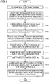
- Fig. 3 is a flowchart illustrating an example of a procedure in which the control device 100 determines whether the photovoltaic strings 200a and 200b have the abnormalities.
- the timing decision unit 112 decides that the present time is the determination timing in which the abnormal determinations of the photovoltaic strings 200a and 200b are made in the case where any one of the above conditions is satisfied (S100). In order to reduce useless power consumption, the control device 100 turns off the connected relay 50 to electrically disconnect the power conditioner 10 and the system power supply 300 from each other (S102).
- the switch controller 102 stops the boost operation of the target boost circuit by turning off the switch of the target boost circuit connected to the photovoltaic string of the determination target (S104). For example, the switch controller 102 turns off the switch Tra of the boost circuit 20a connected to the photovoltaic string 200a of the determination target to stop the boost operation of the target boost circuit 20a.
- the switch controller 102 acquires the voltage value on the input side and the voltage value on the output side of the target boost circuit through the voltage sensor 12a and the voltage sensor 16.
- the switch controller 102 controls the voltage on the output side of the target boost circuit such that the voltage on the output side is greater than or equal to the voltage on the input side of the target boost circuit, namely, the switch controller 102 controls the voltage at the connection unit 30 (S106).
- the switch controller 102 turns on the switch of the target boost circuit to form the closed circuit including the photovoltaic string of the determination target.
- the short-circuit current value acquisition unit 104 acquires the current value, which passes through the closed circuit formed by turning on the switch of the target boost circuit, as the short-circuit current value during the on period of the switch of the target boost circuit (S108). For example, the short-circuit current value acquisition unit 104 acquires the current value, which passes through the first closed circuit during the on period of the switch Tra of the boost circuit 20a, as the first short-circuit current value through the current sensor 14a.
- the power supply abnormality determination unit 106 determines whether the photovoltaic string of the determination target has the abnormality by comparing the acquired short-circuit current value to the reference current value corresponding to the photovoltaic string of the determination target (S112).
- the control device 100 determines whether the determination of the abnormality is made for all the photovoltaic strings (S114). Until the determination of the abnormality is not made for all the photovoltaic strings, the control device 100 repeats the steps of processing from Step S102 to Step S112. For example, after the determination of the abnormality is made for all the photovoltaic strings 200a, the control device 100 determines whether the photovoltaic string 200b has the abnormality.
- the power supply abnormality determination unit 106 may determine whether the photovoltaic string of the determination target has the abnormality based on the reference current value and the plurality of short-circuit current values, which are stored in the storage unit 114 every time the short-circuit current value acquisition unit 104 acquires the short-circuit current value.
- the power supply abnormality determination unit 106 may calculate an average value of the plurality of short-circuit current values, and determine whether the photovoltaic string of the determination target has the abnormality based on the comparison between the average and the reference current value.
- the power supply abnormality determination unit 106 may determine that the photovoltaic string of the determination target has the abnormality when the difference between the acquired short-circuit current value and the reference current value is greater than or equal to the fixed reference difference, and when the condition related to the meteorological information on the illuminance in acquiring the short-circuit current value agrees with the condition related to the meteorological information on the illuminance corresponding to the reference current value.
- the power supply abnormality determination unit 106 may determine that the photovoltaic string of the determination target has the abnormality when the difference between the acquired short-circuit current value and the reference current value is greater than or equal to the fixed reference difference, and when the illuminance in acquiring the short-circuit current value falls within a reference illuminance range fixed based on the illuminance in deciding the reference current value.
- Fig. 4 is a flowchart illustrating an example in which the switch controller 102 controls the voltage at the connection unit 30 such that the voltage at the connection unit 30 is greater than or equal to the voltage on the input side of the target boost circuit connected to the photovoltaic string of the determination target.
- the switch controller 102 acquires the voltage Vin on the input side of the boost circuit connected to the photovoltaic string of the determination target (S200).
- the switch controller 102 performs the boost operation to the boost circuit except the target boost circuit, and controls a voltage Vbus at the connection unit 30 such that the voltage Vbus is greater than or equal to the voltage Vin (S202).
- the switch controller 102 determines whether the voltage Vbus is greater than or equal to the voltage Vin by the boost operation of the boost circuit except the target boost circuit (S204).
- the switch controller 102 turns on the connected relay 50 to electrically connect the power conditioner 10 and the system power supply 300 to each other (S206).
- the switch controller 102 controls the inverter 40, and controls the voltage Vbus using the power supplied from the system power supply 300 such that the voltage Vbus is greater than or equal to the voltage Vin (S208).
- the switch controller 102 performs the PWM control to each switch included in the inverter 40 such that the current output from the inverter 40 is opposite in phase to the AC voltage at the system power supply 300.
- the switch controller 102 can perform the control such that the voltage Vbus is greater than or equal to the voltage Vin.
- the power conditioner 10 includes the two boost circuits by way of example.
- the power conditioner 10 may include at least three boost circuits.
- the switch controller 102 performs the boost operation of one of the three boost circuits while turning on the switch included in the target boost circuit connected to the photovoltaic string of the determination target among the three boost circuits, and the switch controller 102 may control the voltage Vbus at the connection unit 30 such that the voltage Vbus is greater than or equal to the voltage Vin.
- Fig. 5 is a system configuration diagram illustrating an example of an entire configuration of a photovoltaic system according to a modification of the embodiment.
- the photovoltaic system of the modification differs from the photovoltaic system in Fig. 1 in that the boost circuit 20b is provided outside the power conditioner 10.
- the photovoltaic system of the modification also differs from the photovoltaic system in Fig. 1 in that the photovoltaic system of the modification includes a control device 100b that acquires the short-circuit current value of the photovoltaic string 200b and a power supply 60b that supplies the driving power to the control device 100b.
- the output side of the boost circuit 20b that boosts the DC voltage outputted from the photovoltaic string 200b is connected to the input side of the boost circuit 20a provided in the power conditioner 10.
- the power supply 60b is connected to both the ends on the output side of the boost circuit 20b.
- the power supply 60b generates the power indicating the predetermined voltage value from the DC voltage taken out from the output side of the boost circuit 20b, and supplies the generated power to the control device 100b.
- the control device 100b conducts communication with the control device 100 in the wireless or wired manner. Similarly to the control device 100, the control device 100b may include the microcomputer and the wireless antenna. After stopping the boost operation of the boost circuit 20b, the control device 100b turns on the switch Trb to form the second closed circuit of the photovoltaic string 200b in response to a request from the control device 100. During the on period of the switch Trb, the control device 100b acquires the second short-circuit current value of the photovoltaic string 200 through the current sensor 14b, and transmits the acquired second short-circuit current value to the control device 100. Based on the comparison between the acquired second short-circuit current value and the previously-stored second reference current value, the control device 100b may determine whether the photovoltaic string 200b has the abnormality, and transmit the determination result to the control device 100.
- the output of the photovoltaic string 200b may be less than that of the photovoltaic string 200a.
- the photovoltaic modules constituting the photovoltaic strings 200a and 200b may differ from each other in specifications.
- the number of photovoltaic modules constituting the photovoltaic string 200b may be less than the number of photovoltaic modules constituting the photovoltaic string 200a.
- the voltage outputted from the photovoltaic string 200a is greater than that output from the photovoltaic string 200b. Therefore, the voltage on the output side of the boost circuit 20b is greater than that on the input side of the boost circuit 20b while the boost operation of the boost circuit 20b is stopped. In this case, the voltage on the output side of the boost circuit 20b does not fluctuate, when the switch Trb is turned on in order to acquire the second short-circuit current value of the photovoltaic string 200b while the boost operation of the boost circuit 20b is stopped.
- Fig. 6 is a flowchart illustrating an example of a procedure in which the control device 100 of the modification of the embodiment determines whether the photovoltaic string has the abnormality.
- the timing decision unit 112 decides the timing of abnormality determination based on the reception of the message indicating the abnormality determination request from the external management device, the meteorological condition, the outputs of the photovoltaic strings 200a and 200b, or the output power or the internal temperature of the power conditioner 10 (S300).
- the switch controller 102 turns off the switches of the boost circuits 20a and 20b connected to the photovoltaic strings 200a and 200b of the determination targets, and stops the boost operations of the boost circuits 20a and 20b (S302). For example, the switch controller 102 transmits the message stopping the boost operation of the boost circuit 20b to the control device 100b through the transmitter/receiver 110, and the control device 100b may stop the boost operation of the boost circuit 20b.
- the switch controller 102 controls the inverter 40 such that the current output from the inverter 40 is opposite in phase to the output voltage at the system power supply 300, and the switch controller 102 controls the voltage Vbus at the connection unit 30 using the power output from the system power supply 300 such that the voltage Vbus at the connection unit 30 is greater than or equal to the voltage Vin on the input side of the boost circuit 20a (S304).
- the switch controller 102 turns on the switch Tra of the boost circuit 20a (S306).
- the short-circuit current value acquisition unit 104 acquires a total current value of the first short-circuit current value passing through the first closed circuit including the photovoltaic string 200a and the second short-circuit current value passing through the second closed circuit including the photovoltaic string 200b through the current sensor 14a (S308).
- the switch controller 102 turns off the switch Tra of the boost circuit 20a, and turns on the switch Trb of the boost circuit 20b (S310).
- the power supply 60b can supply the driving power to the control device 100b using the power outputted from the photovoltaic string 200a.
- the switch controller of the control device 100b turns on the switch Trb of the boost circuit 20b in response to the message from the control device 100.
- the control device 100b acquires the second short-circuit current value of the photovoltaic string 200b through the current sensor 14b, and transmits the second short-circuit current value to the control device 100 (S312).
- the control device 100b turns off the switch Trb of the boost circuit 20b after transmitting the second short-circuit current value (S314).
- the power supply abnormality determination unit 106 acquires the first short-circuit current value based on the total current value and the second short-circuit current value (S316). The power supply abnormality determination unit 106 may acquire the first short-circuit current value by subtracting the second short-circuit current value from the total current value. The power supply abnormality determination unit 106 compares the acquired first short-circuit current value and second short-circuit current value to the reference current values corresponding to the first and second short-circuit current values, and determines whether each of the photovoltaic strings 200a and 200b has the abnormality (S318).
- the closed circuit of the photovoltaic string can be formed using the existing boost circuit provided in the photovoltaic system. Therefore, in order to acquire the short-circuit current value of the photovoltaic string, it is not necessary to provide a new circuit such as a transistor. Based on the short-circuit current value of the photovoltaic string, a checker can perform remote control of the boost circuit to inspect whether the photovoltaic string has the abnormality without visiting the installation site of the photovoltaic string.
- the transistor provided in the boost circuit is used as the transistor that short-circuits the photovoltaic string.
- a coil or a transformer winding is provided in the boost circuit in order to boost the input voltage.
- the current caused by the floating capacitance can be absorbed by the coil or the transformer winding. Therefore, it is not necessary to add the large-size transistor, which acquires the short-circuit current value, such that the transistor does not break down due to the current caused by the floating capacitance.
- the voltage control operation to control the voltage at the connection unit 30 can be performed by the boost operation of the boost circuit, in which the power from the photovoltaic string except the photovoltaic string of the determination target is used, such that the voltage at the connection unit 30 is greater than or equal to the voltage on the input side of the target boost circuit connected to the photovoltaic string of the determination target. Therefore, the consumption of the power from the system power supply 300 in association with the voltage control operation can be reduced as little as possible.
- a program which is stored in a computer-readable recording medium to perform various pieces of processing related to the acquisition of the short-circuit current value and the abnormality determination of the photovoltaic string, is installed in a computer, and each unit included in the control device 100 may be constructed by causing the computer to execute the program. That is, the computer is caused to execute the program to perform various pieces of processing related to the acquisition of the short-circuit current value and the abnormality determination of the photovoltaic string, and the computer acts as each unit included in the control device 100, whereby the control device 100 may be constructed.
- the computer includes a CPU, memories such as a ROM, a RAM, and an EEPROM (registered trademark), a communication bus, and an interface, and the CPU reads and executes sequentially the processing program previously stored in the ROM as firmware, whereby the computer acts as the control device 100.
- memories such as a ROM, a RAM, and an EEPROM (registered trademark)
- EEPROM registered trademark
Landscapes
- Engineering & Computer Science (AREA)
- Power Engineering (AREA)
- Inverter Devices (AREA)
- Photovoltaic Devices (AREA)
- Dc-Dc Converters (AREA)
- Supply And Distribution Of Alternating Current (AREA)
Description
- The present invention relates to a power conditioner, a photovoltaic system, and an abnormality determination method.
- Sometimes a short-circuit current value of a power supply such as a photovoltaic cell is used as a parameter to determine whether the power supply has an abnormality. In a photovoltaic power system disclosed in Japanese Unexamined Patent Publication No.
2001-257377 - The following documents relate to further technological background of the present invention:
D1 US 2008/094867 A1 (MULLER BURKARD [DE] ET AL) 24 April 2008 (2008-04-24)D2 CN 102 608 512 A (UNIV SHANGHAI ELECTRIC POWER) 25 July 2012 (2012-07-25)D3 MYRZIK J M A ET AL: "String and module integrated inverters for single-phase grid connected photovoltaic systems - a review", CONFERENCE PROCEEDINGS / 2003 IEEE BOLOGNA POWER TECH: JUNE 23 - 26, 2003, FACULTY OF ENGINEERING, UNIVERSITY OF BOLOGNA, BOLOGNA, ITALY, PISCATAWAY, NJ : IEEE SERVICE CENTER, US, vol. 2, 23 June 2003 (2003-06-23), pages 1-8, XP002523862, ISBN: 978-0-7803-7967-1 - Document D1 discloses a power conditioner that boosts a direct current outputted from a first power supply and the power conditioner converts the boosted direct current into an alternating current and outputs the converted alternating current to a system power supply. The power conditioner comprises a first boost circuit, an inverter, a connection unit configured to connect an output side of the first boost circuit and an input side of the inverter, a controlling of the voltage at the connection unit and the generation of a short-circuit between the output terminals of the first power supply to form a first closed circuit of the first power supply. Further, a short-circuit current value acquisition unit is used to acquire a first short-circuit current value passing through the first closed circuit during a period and a buffer capacitor is connected to a DC bus between the first boost circuit and the inverter.
- Document D2 discloses fault detection based on voltage waveform comparison.
- The object of the present invention is to provide a power conditioner and an abnormality determination unit to detect the short-circuit current value of the power supply such as the photovoltaic cell without adding a new circuit such as the transistor. This object is solved by a power conditioner of
claim 1 and an abnormality determination unit according to claim 12. Further advantageous embodiments and improvements of the present invention are listed in the dependent claims. Hereinafter, before coming to detailed discussion of the embodiments of the invention with reference to the attached drawings, some aspects of the invention which contribute to the understanding of the invention are discussed separately below. - In accordance with a first aspect of the present invention, a power conditioner that boosts a direct current outputted from a first power supply, converts boosted direct current into an alternating current, and outputs the converted alternating current to a system power supply. The power conditioner includes: a first boost circuit that includes a first switch connected between output terminals of the first power supply and is configured to boost the direct current from the first power supply by turning on and off the first switch; an inverter configured to convert the direct current outputted from the first boost circuit into the alternating current; a connection unit configured to connect an output side of the first boost circuit and an input side of the inverter; a controller configured to turn on the first switch while setting the output side of the first boost circuit to a voltage higher than a voltage on the input side of the first boost circuit by controlling the voltage at the connection unit, and to generate a short-circuit between the output terminals of the first power supply to form a first closed circuit of the first power supply; a short-circuit current value acquisition unit configured to acquire a first short-circuit current value passing through the first closed circuit during a period, when the controller turns on the first switch while setting the output side of the first boost circuit to the voltage higher than the voltage on the input side of the first boost circuit by controlling the voltage at the connection unit; and a power supply abnormality determination unit configured to determine whether the first power supply has an abnormality based on comparison between the first short-circuit current value and a first reference current value, the first reference current value being previously fixed based on a characteristic of the first power supply.
- In the power conditioner, the first boost circuit may further include a first backflow prevention circuit configured to prevent inflow of a current from the output side of the first boost circuit.
- The power conditioner may further include a second boost circuit that includes a second switch connected between output terminals of a second power supply and is configured to boost the direct current from the second power supply by turning on and off the second switch. In the power conditioner, a connection unit connects the output side of the first boost circuit and an output side of the second boost circuit in parallel to each other; and the controller may turn on and off the second switch to control the voltage at the connection unit, and set the output side of the first boost circuit to the voltage higher than the voltage on the input side of the first boost circuit.
- In the power conditioner, the controller may control the inverter to control the voltage at the connection unit, and set the output side of the first boost circuit to the voltage higher than the voltage on the input side of the first boost circuit, when the controller turns on and off the second switch to control the voltage at the connection unit and cannot set the output side of the first boost circuit to the voltage higher than the voltage on the input side of the first boost circuit.
- In the power conditioner, the controller may turn on and off the first switch to control the voltage at the connection unit, turn on the second switch while setting the output side of the second boost circuit to the voltage higher than the voltage on the input side of the second boost circuit, and generate the short-circuit between the output terminals of the second power supply to form a second closed circuit of the second power supply, the short-circuit current value acquisition unit may acquire a second short-circuit current value passing through the second closed circuit during a period, when the controller turns on and off the first switch to control the voltage at the connection unit and turns on the second switch while setting the output side of the second boost circuit to the voltage higher than the voltage on the input side of the second boost circuit, and the power supply abnormality determination unit may determine whether the second power supply has the abnormality based on comparison between the second short-circuit current value and a second reference current value, the second reference current value being previously fixed based on a characteristic of the second power supply.
- In the power conditioner, the second boost circuit may further include a second backflow prevention circuit configured to prevent inflow of the current from the output side of the second boost circuit.
- In the power conditioner, the controller may control the inverter to output a power from the system power supply onto the side of the connection unit, and control the voltage at the connection unit to set the output side of the first boost circuit to the voltage higher than the voltage on the input side of the first boost circuit.
- In accordance with a second aspect of the present invention, a photovoltaic system includes: a first photovoltaic cell that is the first power supply; and the power conditioner configured to convert the direct current outputted from the first photovoltaic cell into the alternating current and to output the alternating current onto the side of the system power supply.
- In accordance with a third aspect of the present invention, a photovoltaic system includes: a first photovoltaic cell that is of the first power supply; a second photovoltaic cell that is of the second power supply connected in parallel to the first photovoltaic cell; and the power conditioner configured to convert the direct currents outputted from the first and second photovoltaic cells into the alternating currents and to output the alternating currents onto the side of the system power supply.
- In accordance with a fourth aspect of the present invention, an abnormality determination method for determining an abnormality of a first power supply connected to a power conditioner, the power conditioner including a first boost circuit that includes the first switch connected between output terminals of the first power supply and is configured to boost the direct current from the first power supply by turning on and off the first switch, an inverter configured to convert the direct current outputted from the first boost circuit into the alternating current, and a connection unit configured to connect an output side of the first boost circuit and an input side of the inverter; the power conditioner boosting the direct current outputted from the first power supply, converting the boosted direct current into an alternating current, and outputting the converted alternating current onto a side of a system power supply, and the abnormality determination method includes: a step of turning on the first switch while setting the output side of the first boost circuit to a voltage higher than a voltage on the input side of the first boost circuit by controlling the voltage at the connection unit, and generating a short-circuit between the output terminals of the first power supply to form a first closed circuit of the first power supply; a step of acquiring a first short-circuit current value passing through the first closed circuit in a period, during which the first switch is turned on while setting the output side of the first boost circuit to the voltage higher than the voltage on the input side of the first boost circuit by controlling the voltage at the connection unit; and a step of determining whether the first power supply has an abnormality based on comparison between the first short-circuit current value and a first reference current value, the first reference current value being previously fixed based on a characteristic of the first power supply.
- In the abnormality determination method, the power conditioner may further include a second boost circuit that includes a second switch connected between output terminals of a second power supply and is configured to boost the direct current from the second power supply by turning on and off the second switch, the connection unit may connect the output side of the first boost circuit and the output side of the second boost circuit in parallel to each other; and, in the first closed circuit forming step, the second switch may be turned on and off to control the voltage at the connection unit, and the output side of the first boost circuit may be set to the voltage higher than the voltage on the input side of the first boost circuit.
- In the abnormality determination method, in the first closed circuit forming step, the inverter may be controlled to control the voltage at the connection unit, and the output side of the first boost circuit may be set to the voltage higher than the voltage on the input side of the first boost circuit, when the second switch cannot be turned on and off to control the voltage at the connection unit and when the output side of the first boost circuit cannot be set to the voltage higher than the voltage on the input side of the first boost circuit.
- The abnormality determination method may further include a step of turning on and off the first switch to control the voltage at the connection unit, turning on the second switch while setting the output side of the second boost circuit to the voltage higher than the voltage on the input side of the second boost circuit, and generating the short-circuit between the output terminals of the second power supply to form a second closed circuit of the second power supply; a step of acquiring a second short-circuit current value passing through the second closed circuit in a period, during which the first switch is turned on and off to control the voltage at the connection unit and the second switch is turned on while the output side of the second boost circuit is set to the voltage higher than the voltage on the input side of the second boost circuit, and a step of determining whether the second power supply has the abnormality based on comparison between the second short-circuit current value and a second reference current value, the second reference current value being previously fixed based on a characteristic of the second power supply.
- All the features necessary for the present invention are not described in the summary of the present invention. A sub-combination of a feature group is also included in the present invention.
-
-
Fig. 1 is a system configuration diagram illustrating an example of an entire configuration of a photovoltaic system according to an embodiment; -
Fig. 2 is a view illustrating an example of a functional block of a control device of the embodiment; -
Fig. 3 is a flowchart illustrating an example of a procedure in which the control device determines whether a photovoltaic string has an abnormality; -
Fig. 4 is a flowchart illustrating an example in which a switch controller controls a voltage at a connection unit such that the voltage is greater than or equal to a voltage on an input side of a boost circuit connected to the photovoltaic string of a determination target; -
Fig. 5 is a system configuration diagram illustrating an example of an entire configuration of a photovoltaic system according to a modification of the embodiment; and -
Fig. 6 is a flowchart illustrating an example of a procedure in which a control device of the modification of the embodiment determines whether a photovoltaic string has an abnormality. - Hereinafter, an embodiment of the present invention will be described. However, the present invention according to the claims is not limited to the embodiment. All combinations of features described in the embodiment are not necessary for the means for solving the problem of the invention.
-
Fig. 1 is a system configuration diagram illustrating an example of an entire configuration of a photovoltaic system of the embodiment. The photovoltaic system includesphotovoltaic strings power conditioner 10. Each of thephotovoltaic strings photovoltaic strings - The
power conditioner 10 boosts the DC voltages outputted from thephotovoltaic strings system power supply 300. - The
power conditioner 10 includes capacitors C1a and C1b,boost circuits connection unit 30, a capacitor C2, aninverter 40, a coil L2, a capacitor C3, a connectedrelay 50, apower supply 60, and acontrol device 100. - Both ends of the capacitor C1a are electrically connected to a positive electrode terminal and a negative electrode terminal of the
photovoltaic string 200a, respectively, and the capacitor C1a smoothes the DC voltage outputted from thephotovoltaic string 200a. Theboost circuit 20a includes a coil L1a, a switch Tra, and a diode Da. Theboost circuit 20a is called a chopper switching regulator. - The switch Tra is an example of the first switch connected between the positive electrode terminal and the negative electrode terminal of the
photovoltaic string 200a. For example, the switch Tra may be an Insulated Gate Bipolar Transistor (IGBT). One end of the coil L1a is connected to one end of the capacitor C1a, and the other end of the coil L1a is connected to a collector of the switch Tra. The collector of the switch Tra is connected to an anode of the diode Da, and an emitter of the switch Tra is connected to the other end of the capacitor C1a. The coil L1a accumulates energy based on power from thephotovoltaic string 200a during an on period of the switch Tra, and discharges the energy accumulated during an off period of the switch Tra. Therefore, theboost circuit 20a boosts the DC voltage outputted from thephotovoltaic string 200a. The diode Da is provided between the switch Tra and theconnection unit 30, and prevents the boosted DC voltage from flowing onto an input side from an output side of theboost circuit 20a. The diode Da is an example of the first backflow prevention element. - Both ends of the capacitor C1b are electrically connected to a positive electrode terminal and a negative electrode terminal of the
photovoltaic string 200b, respectively, and the capacitor C1b smoothes the DC voltage outputted from thephotovoltaic string 200b. Theboost circuit 20b includes a coil L1b, a switch Trb, and a diode Db. Theboost circuit 20b may be what is called a chopper switching regulator. - The switch Trb is an example of the second switch connected between the positive electrode terminal and the negative electrode terminal of the
photovoltaic string 200b. For example, the switch Trb may be an Insulated Gate Bipolar Transistor (IGBT). One end of the coil L1b is connected to one end of the capacitor C1b, and the other end of the coil L1a is connected to a collector of the switch Trb. The collector of the switch Trb is connected to an anode of the diode Db, and an emitter of the switch Trb is connected to the other end of the capacitor C1b. The coil L1b accumulates energy based on the power from thephotovoltaic string 200b during the on period of the switch Trb, and discharges the energy accumulated during the off period of the switch Trb. Therefore, theboost circuit 20b boosts the DC voltage outputted from thephotovoltaic string 200b. The diode Db is provided between the switch Trb and theconnection unit 30, and prevents the boosted DC voltage from flowing onto the input side from the output side of theboost circuit 20b. The diode Db is an example of the second backflow prevention element. - The
boost circuits boost circuits photovoltaic string 200a or thephotovoltaic string 200b. The plurality of switches are connected in series with the primary winding. By turning on and off the plurality of switches, an exciting current is passed through the primary winding while an induced current is passed through the secondary winding. In the case where the boost circuit included in the photovoltaic system is the insulation type boost circuit, such as the full-bridge boost circuit, which has the transformer winding, the plurality of switches, which are connected in series with the primary winding and connected between the output terminals of the power supply, act as the first switch or the second switch. - The
connection unit 30 connects the output side of theboost circuit 20a and the output side of theboost circuit 20b in parallel to each other. The capacitor C2 smooths the DC voltage outputted from theconnection unit 30. Theinverter 40 includes a switch, and converts the DC voltages outputted from theboost circuits inverter 40 may be constructed as a single-phase full-bridge PWM inverter including four bridge-connected semiconductor switches. In one pair out of the four semiconductor switches, the semiconductor switches are connected in series. In the other pair out of the four semiconductor switches, the semiconductor switches are connected in series. The other pair of semiconductor switches is connected in parallel to the one pair of semiconductor switches. - The coil L2 and the capacitor C3 are provided between the
inverter 40 and thesystem power supply 300. The coil L2 and the capacitor C3 remove a noise from the AC voltage outputted from theinverter 40. Theconnected relay 50 is provided between the capacitor C3 and thesystem power supply 300. Thepower conditioner 10 and thesystem power supply 300 are electrically connected to each other by turning on theconnected relay 50, and thepower conditioner 10 and thesystem power supply 300 are electrically disconnected from each other by turning off theconnected relay 50. - For example, the
power supply 60 is constructed by a power supply IC chip. Thepower supply 60 is connected to both the ends of theconnection unit 30. Thepower supply 60 generates power indicating a predetermined voltage value from the DC voltage taken out from theconnection unit 30, and supplies the generated power to thecontrol device 100. - In order to obtain the maximum power from the
photovoltaic strings control device 100 controls the switching operations of theboost circuits inverter 40, boosts the DC voltages outputted from thephotovoltaic strings system power supply 300. - The
power conditioner 10 also includesvoltage sensors current sensors voltage sensor 16. Thevoltage sensor 12a detects a voltage value Vain corresponding to a potential difference at both the ends of thephotovoltaic string 200a. Thevoltage sensor 12b detects a voltage value Vbin corresponding to a potential difference at both the ends of thephotovoltaic string 200b. Thecurrent sensor 14a detects a current value lain corresponding to the current outputted fromphotovoltaic string 200a. Thecurrent sensor 14b detects a current value Ibin corresponding to the current outputted fromphotovoltaic string 200b. Thevoltage sensor 16 detects a voltage value Vout corresponding to a potential difference at both the ends of theconnection unit 30. - In the photovoltaic system having the above configuration, short-circuit current values of the
photovoltaic strings photovoltaic strings -
Fig. 2 is a view illustrating an example of a functional block of thecontrol device 100. Thecontrol device 100 acts as the short-circuit current detection device. Thecontrol device 100 includes aswitch controller 102, a short-circuit currentvalue acquisition unit 104, a power supplyabnormality determination unit 106, a meteorologicalinformation acquisition unit 108, a transmitter/receiver 110, atiming decision unit 112, and astorage unit 114. Theswitch controller 102, the short-circuit currentvalue acquisition unit 104, the power supplyabnormality determination unit 106, the meteorologicalinformation acquisition unit 108, thetiming decision unit 112, and thestorage unit 114 may be constructed by a microcomputer. The transmitter/receiver 110 may be constructed by a wireless antenna. - The
switch controller 102 is an example of the controller. Theswitch controller 102 accumulates the energy based on the power outputted from thephotovoltaic string 200a in the coil L1a during the on period of the switch Tra by turning on and off the switch Tra included in theboost circuit 20a, and boosts the voltage at thephotovoltaic string 200a using theboost circuit 20a by discharging the energy from the coil L1a during the off period of the switch Tra. Theswitch controller 102 accumulates the energy based on the power outputted from thephotovoltaic string 200b in the coil L1b during the on period of the switch Trb by turning on and off the switch Trb included in theboost circuit 20b, and boosts the voltage at thephotovoltaic string 200b using theboost circuit 20b by discharging the energy from the coil L1b during the off period of the switch Trb. - When acquiring the first short-circuit current value that is of the short-circuit current value of the
photovoltaic string 200a, theswitch controller 102 stops the boost operation of theboost circuit 20a to turn on the switch Tra, thereby forming the first closed circuit of thephotovoltaic string 200a. When acquiring the second short-circuit current value that is of the short-circuit current value of thephotovoltaic string 200b, theswitch controller 102 stops the boost operation of theboost circuit 20b to turn on the switch Trb, thereby forming the second closed circuit of thephotovoltaic string 200b. - The short-circuit current
value acquisition unit 104 acquires the first short-circuit current value passing through the first closed circuit when the switch Tra is in the on period while the boost operation of theboost circuit 20a is stopped. The short-circuit currentvalue acquisition unit 104 acquires the second short-circuit current value passing through the second closed circuit when the switch Trb is in the on period while the boost operation of theboost circuit 20b is stopped. - At this point, the
power supply 60 may acquire a driving power, which is of the power used to drive itself, from theconnection unit 30. In the case where the voltage on the input side of theboost circuit 20a is less than that on the output side, the current flows partially onto the side of theinverter 40 from thephotovoltaic string 200a through the diode Da. Therefore, the voltage at both the ends of the capacitor C2 fluctuates. That is, the voltage at both the ends of theconnection unit 30 fluctuates. When the voltage at both the ends of theconnection unit 30 fluctuates, the power supplied to thepower supply 60 becomes unstable, and possibly the power is unstably supplied to thecontrol device 100 from thepower supply 60. For this reason, preferably the voltage on the output side of theboost circuit 20a is greater than that on the input side. This enables the current to be prevented from flowing partially onto the side of theinverter 40 from thephotovoltaic string 200a through the diode Da. Therefore, the power is stably supplied to thepower supply 60 because the voltage at both the ends of theconnection unit 30 stabilizes, so that thepower supply 60 can stably supply the power to thecontrol device 100. Thepower supply 60 may directly take the power from thesystem power supply 300, and generate the power supplied to thecontrol device 100 based on the power output from thesystem power supply 300. - In the case where the short-circuit current
value acquisition unit 104 acquires the first short-circuit current value, in order to stably supply the power to thecontrol device 100 from thepower supply 60, theswitch controller 102 may control the voltage at theconnection unit 30 to set the voltage on the output side of theboost circuit 20a higher than the voltage on the input side of theboost circuit 20a. Theswitch controller 102 may control the voltage at theconnection unit 30 such that the voltage at theconnection unit 30 is greater than or equal to the voltage on the input side of theboost circuit 20a by turning on and off the switch Trb included in theboost circuit 20b. In the case where the short-circuit currentvalue acquisition unit 104 acquires the first short-circuit current value, theswitch controller 102 may turn on the switch Tra while setting the voltage on the output side of theboost circuit 20a higher than the voltage on the input side of theboost circuit 20a, and generate a short-circuit between the output terminals of thephotovoltaic string 200a to form the first closed circuit of thephotovoltaic string 200a. In the case where the short-circuit currentvalue acquisition unit 104 acquires the second short-circuit current value, in order to stably supply the power to thecontrol device 100 from thepower supply 60, theswitch controller 102 may control the voltage at theconnection unit 30 to set the voltage on the output side of theboost circuit 20b higher than the voltage on the input side of theboost circuit 20b. Theswitch controller 102 may control the voltage at theconnection unit 30 such that the voltage at theconnection unit 30 is greater than or equal to the voltage on the input side of theboost circuit 20b by turning on and off the switch Tra included in theboost circuit 20a. In the case where the short-circuit currentvalue acquisition unit 104 acquires the second short-circuit current value, theswitch controller 102 may turn on the switch Trb while setting the voltage on the output side of theboost circuit 20b higher than the voltage on the input side of theboost circuit 20b, and generate the short-circuit between the output terminals of thephotovoltaic string 200b to form the second closed circuit of thephotovoltaic string 200b. - At this point, depending on a meteorological condition, sometimes a small amount of power is obtained from the
photovoltaic string 200a or thephotovoltaic string 200b, and the voltage at theconnection unit 30 hardly increases greater than or equal to the voltage on the input side of theboost circuit 20b or the voltage on the input side of theboost circuit 20a by the boost operation of theboost circuit switch controller 102 may control each switch included in theinverter 40, and increase the voltage at theconnection unit 30 such that the voltage at theconnection unit 30 is greater than or equal to the voltage on the input side of theboost circuit 20b or the voltage on the input side of theboost circuit 20a based on the power from thesystem power supply 300. - In the case where the voltage at the
connection unit 30 hardly increases greater than or equal to the voltage on the input side of theboost circuit 20a by controlling the switch Trb included in theboost circuit 20b, theswitch controller 102 may output the power onto the side of theconnection unit 30 from thesystem power supply 300 by turning on and off each switch included in theinverter 40, and increase the voltage at theconnection unit 30 such that the voltage at theconnection unit 30 is greater than or equal to the voltage on the input side of theboost circuit 20a. In the case where the voltage at theconnection unit 30 hardly increases greater than or equal to the voltage on the input side of theboost circuit 20a by controlling the switch Tra included in theboost circuit 20a, theswitch controller 102 may output the power onto the side of theconnection unit 30 from thesystem power supply 300 by turning on and off each switch included in theinverter 40, and increase the voltage at theconnection unit 30 such that the voltage at theconnection unit 30 is greater than or equal to the voltage on the input side of theboost circuit 20b. Theswitch controller 102 can output the power to theinverter 40 on the side of theconnection unit 30 from thesystem power supply 300 by performing PWM control to each switch included in theinverter 40 such that the current outputted from theinverter 40 is opposite in phase to the voltage at thesystem power supply 300. - The power supply
abnormality determination unit 106 determines whether thephotovoltaic string 200a has an abnormality based on comparison between the first short-circuit current value and the first reference current value that is previously fixed based on a characteristic of thephotovoltaic string 200a. The power supplyabnormality determination unit 106 determines whether thephotovoltaic string 200b has an abnormality based on comparison between the second short-circuit current value and the second reference current value that is previously fixed based on a characteristic of thephotovoltaic string 200b. Possibly outputs of thephotovoltaic string 200a and thephotovoltaic string 200b decrease due to degradation and the like. The detected short-circuit current also decreases in the case where the outputs decrease. Therefore, the power supplyabnormality determination unit 106 may determine that thephotovoltaic string - The power supply
abnormality determination unit 106 may decide that the first or second short-circuit current value, which is initially acquired on the predetermined meteorological condition by the short-circuit currentvalue acquisition unit 104, is the first or second reference current value. The power supplyabnormality determination unit 106 may decide that the first or second short-circuit current value, which is initially acquired by the short-circuit currentvalue acquisition unit 104 when the outputs of thephotovoltaic strings abnormality determination unit 106 may decide that the first or second short-circuit current value when the output power of thepower conditioner 10 is a predetermined value, which is initially acquired by the short-circuit currentvalue acquisition unit 104, is the first or second reference current value. The power supplyabnormality determination unit 106 may decide that the first or second short-circuit current value when an internal temperature of thepower conditioner 10 is a predetermined value, which is initially acquired by the short-circuit currentvalue acquisition unit 104, is the first or second reference current value. - The power supply
abnormality determination unit 106 compares the decided first or second reference current value to the first or second short-circuit current value presently acquired by the short-circuit currentvalue acquisition unit 104. The power supplyabnormality determination unit 106 may determine that thephotovoltaic string - The meteorological
information acquisition unit 108 acquires meteorological information around a site where thephotovoltaic strings photovoltaic strings receiver 110 conducts communication with the outside in a wireless or wired manner. The transmitter/receiver 110 may receive a message to provide a command to determine the abnormalities of thephotovoltaic strings receiver 110 may transmit a determination result of the power supplyabnormality determination unit 106 to the external management device. The transmitter/receiver 110 may transmit the first and second short-circuit current values acquired by the short-circuit currentvalue acquisition unit 104 to the external management device and the like. - The
timing decision unit 112 decides determination timing indicating the time the power supplyabnormality determination unit 106 determines whether thephotovoltaic strings timing decision unit 112 may decide the determination timing based on the meteorological information acquired by the meteorologicalinformation acquisition unit 108. Thetiming decision unit 112 may decide that a present time is the determination timing in the case where the present meteorological condition agrees with the meteorological condition at the time the first and second reference current values are decided. - The
timing decision unit 112 may decide that the present time is the determination timing in the case where each of the current outputs of thephotovoltaic strings timing decision unit 112 may decide that the present time is the determination timing in the case where the current output power of thepower conditioner 10 is included in a reference range, which is fixed based on the output power when the first and second reference current values are acquired. Thetiming decision unit 112 may decide that the present time is the determination timing in the case where the current internal temperature of thepower conditioner 10 is included in a reference range, which is fixed based on the internal temperature when the first and second reference current values are acquired. - The
timing decision unit 112 may decide that the present time is the determination timing in the case where a present date becomes a predetermined date. Alternatively, thetiming decision unit 112 may decide the determination timing every time the number of start-up times of thepower conditioner 10 becomes predetermined times. Thetiming decision unit 112 may decide the determination timing at the time at least one of parameters including the meteorological condition, the outputs of thephotovoltaic strings power conditioner 10, and the internal temperature of thepower conditioner 10 is included in the initially-fixed reference range after the present date becomes the predetermined date or after the number of start-up times of thepower conditioner 10 reaches the predetermined times. - The
timing decision unit 112 may decide that the present time is the determination timing in the case where the transmitter/receiver 110 receives the message to provide the command to determine the abnormality from the external management device. - The
timing decision unit 112 may decide the determination timing at the time at least one of parameters including the meteorological condition, the outputs of thephotovoltaic strings power conditioner 10, and the internal temperature of thepower conditioner 10 is included in the initially-fixed reference range after the transmitter/receiver 110 receives the message to provide the command to determine the abnormality from the external management device. - The first and second reference current values, the meteorological condition for deciding the abnormality determination timing, the outputs of the
photovoltaic strings power conditioner 10 are stored in thestorage unit 114. -
Fig. 3 is a flowchart illustrating an example of a procedure in which thecontrol device 100 determines whether thephotovoltaic strings - The
timing decision unit 112 decides that the present time is the determination timing in which the abnormal determinations of thephotovoltaic strings control device 100 turns off theconnected relay 50 to electrically disconnect thepower conditioner 10 and thesystem power supply 300 from each other (S102). - Subsequently, the
switch controller 102 stops the boost operation of the target boost circuit by turning off the switch of the target boost circuit connected to the photovoltaic string of the determination target (S104). For example, theswitch controller 102 turns off the switch Tra of theboost circuit 20a connected to thephotovoltaic string 200a of the determination target to stop the boost operation of thetarget boost circuit 20a. - The
switch controller 102 acquires the voltage value on the input side and the voltage value on the output side of the target boost circuit through thevoltage sensor 12a and thevoltage sensor 16. Theswitch controller 102 controls the voltage on the output side of the target boost circuit such that the voltage on the output side is greater than or equal to the voltage on the input side of the target boost circuit, namely, theswitch controller 102 controls the voltage at the connection unit 30 (S106). - The
switch controller 102 turns on the switch of the target boost circuit to form the closed circuit including the photovoltaic string of the determination target. The short-circuit currentvalue acquisition unit 104 acquires the current value, which passes through the closed circuit formed by turning on the switch of the target boost circuit, as the short-circuit current value during the on period of the switch of the target boost circuit (S108). For example, the short-circuit currentvalue acquisition unit 104 acquires the current value, which passes through the first closed circuit during the on period of the switch Tra of theboost circuit 20a, as the first short-circuit current value through thecurrent sensor 14a. - The power supply
abnormality determination unit 106 determines whether the photovoltaic string of the determination target has the abnormality by comparing the acquired short-circuit current value to the reference current value corresponding to the photovoltaic string of the determination target (S112). Thecontrol device 100 determines whether the determination of the abnormality is made for all the photovoltaic strings (S114). Until the determination of the abnormality is not made for all the photovoltaic strings, thecontrol device 100 repeats the steps of processing from Step S102 to Step S112. For example, after the determination of the abnormality is made for all thephotovoltaic strings 200a, thecontrol device 100 determines whether thephotovoltaic string 200b has the abnormality. - The power supply
abnormality determination unit 106 may determine whether the photovoltaic string of the determination target has the abnormality based on the reference current value and the plurality of short-circuit current values, which are stored in thestorage unit 114 every time the short-circuit currentvalue acquisition unit 104 acquires the short-circuit current value. The power supplyabnormality determination unit 106 may calculate an average value of the plurality of short-circuit current values, and determine whether the photovoltaic string of the determination target has the abnormality based on the comparison between the average and the reference current value. The power supplyabnormality determination unit 106 may determine that the photovoltaic string of the determination target has the abnormality when the difference between the acquired short-circuit current value and the reference current value is greater than or equal to the fixed reference difference, and when the condition related to the meteorological information on the illuminance in acquiring the short-circuit current value agrees with the condition related to the meteorological information on the illuminance corresponding to the reference current value. For example, the power supplyabnormality determination unit 106 may determine that the photovoltaic string of the determination target has the abnormality when the difference between the acquired short-circuit current value and the reference current value is greater than or equal to the fixed reference difference, and when the illuminance in acquiring the short-circuit current value falls within a reference illuminance range fixed based on the illuminance in deciding the reference current value. -
Fig. 4 is a flowchart illustrating an example in which theswitch controller 102 controls the voltage at theconnection unit 30 such that the voltage at theconnection unit 30 is greater than or equal to the voltage on the input side of the target boost circuit connected to the photovoltaic string of the determination target. - The
switch controller 102 acquires the voltage Vin on the input side of the boost circuit connected to the photovoltaic string of the determination target (S200). Theswitch controller 102 performs the boost operation to the boost circuit except the target boost circuit, and controls a voltage Vbus at theconnection unit 30 such that the voltage Vbus is greater than or equal to the voltage Vin (S202). Theswitch controller 102 determines whether the voltage Vbus is greater than or equal to the voltage Vin by the boost operation of the boost circuit except the target boost circuit (S204). - For example, sometimes the photovoltaic string connected to the boost circuit except the target boost circuit has the low output because the illuminance is low for the photovoltaic string, and the voltage Vbus at the
connection unit 30 is hardly controlled by the boost operation of the boost circuit such that the voltage Vbus is greater than or equal to the voltage Vin. In such cases, theswitch controller 102 turns on theconnected relay 50 to electrically connect thepower conditioner 10 and thesystem power supply 300 to each other (S206). Theswitch controller 102 controls theinverter 40, and controls the voltage Vbus using the power supplied from thesystem power supply 300 such that the voltage Vbus is greater than or equal to the voltage Vin (S208). For example, theswitch controller 102 performs the PWM control to each switch included in theinverter 40 such that the current output from theinverter 40 is opposite in phase to the AC voltage at thesystem power supply 300. Through the above processing, theswitch controller 102 can perform the control such that the voltage Vbus is greater than or equal to the voltage Vin. - In the embodiment, the
power conditioner 10 includes the two boost circuits by way of example. Alternatively, thepower conditioner 10 may include at least three boost circuits. In the case where thepower conditioner 10 includes three boost circuits, theswitch controller 102 performs the boost operation of one of the three boost circuits while turning on the switch included in the target boost circuit connected to the photovoltaic string of the determination target among the three boost circuits, and theswitch controller 102 may control the voltage Vbus at theconnection unit 30 such that the voltage Vbus is greater than or equal to the voltage Vin. -
Fig. 5 is a system configuration diagram illustrating an example of an entire configuration of a photovoltaic system according to a modification of the embodiment. The photovoltaic system of the modification differs from the photovoltaic system inFig. 1 in that theboost circuit 20b is provided outside thepower conditioner 10. The photovoltaic system of the modification also differs from the photovoltaic system inFig. 1 in that the photovoltaic system of the modification includes acontrol device 100b that acquires the short-circuit current value of thephotovoltaic string 200b and apower supply 60b that supplies the driving power to thecontrol device 100b. - The output side of the
boost circuit 20b that boosts the DC voltage outputted from thephotovoltaic string 200b is connected to the input side of theboost circuit 20a provided in thepower conditioner 10. Thepower supply 60b is connected to both the ends on the output side of theboost circuit 20b. Thepower supply 60b generates the power indicating the predetermined voltage value from the DC voltage taken out from the output side of theboost circuit 20b, and supplies the generated power to thecontrol device 100b. - The
control device 100b conducts communication with thecontrol device 100 in the wireless or wired manner. Similarly to thecontrol device 100, thecontrol device 100b may include the microcomputer and the wireless antenna. After stopping the boost operation of theboost circuit 20b, thecontrol device 100b turns on the switch Trb to form the second closed circuit of thephotovoltaic string 200b in response to a request from thecontrol device 100. During the on period of the switch Trb, thecontrol device 100b acquires the second short-circuit current value of thephotovoltaic string 200 through thecurrent sensor 14b, and transmits the acquired second short-circuit current value to thecontrol device 100. Based on the comparison between the acquired second short-circuit current value and the previously-stored second reference current value, thecontrol device 100b may determine whether thephotovoltaic string 200b has the abnormality, and transmit the determination result to thecontrol device 100. - At this point, the output of the
photovoltaic string 200b may be less than that of thephotovoltaic string 200a. The photovoltaic modules constituting thephotovoltaic strings photovoltaic strings photovoltaic string 200b may be less than the number of photovoltaic modules constituting thephotovoltaic string 200a. - In the case where the
photovoltaic strings photovoltaic string 200a is greater than that output from thephotovoltaic string 200b. Therefore, the voltage on the output side of theboost circuit 20b is greater than that on the input side of theboost circuit 20b while the boost operation of theboost circuit 20b is stopped. In this case, the voltage on the output side of theboost circuit 20b does not fluctuate, when the switch Trb is turned on in order to acquire the second short-circuit current value of thephotovoltaic string 200b while the boost operation of theboost circuit 20b is stopped. -
Fig. 6 is a flowchart illustrating an example of a procedure in which thecontrol device 100 of the modification of the embodiment determines whether the photovoltaic string has the abnormality. - The
timing decision unit 112 decides the timing of abnormality determination based on the reception of the message indicating the abnormality determination request from the external management device, the meteorological condition, the outputs of thephotovoltaic strings switch controller 102 turns off the switches of theboost circuits photovoltaic strings boost circuits switch controller 102 transmits the message stopping the boost operation of theboost circuit 20b to thecontrol device 100b through the transmitter/receiver 110, and thecontrol device 100b may stop the boost operation of theboost circuit 20b. - The
switch controller 102 controls theinverter 40 such that the current output from theinverter 40 is opposite in phase to the output voltage at thesystem power supply 300, and theswitch controller 102 controls the voltage Vbus at theconnection unit 30 using the power output from thesystem power supply 300 such that the voltage Vbus at theconnection unit 30 is greater than or equal to the voltage Vin on the input side of theboost circuit 20a (S304). - The
switch controller 102 turns on the switch Tra of theboost circuit 20a (S306). During the on period of theboost circuit 20a, the short-circuit currentvalue acquisition unit 104 acquires a total current value of the first short-circuit current value passing through the first closed circuit including thephotovoltaic string 200a and the second short-circuit current value passing through the second closed circuit including thephotovoltaic string 200b through thecurrent sensor 14a (S308). - The
switch controller 102 turns off the switch Tra of theboost circuit 20a, and turns on the switch Trb of theboost circuit 20b (S310). Here, when the switch Tra of theboost circuit 20a is turned off, thepower supply 60b can supply the driving power to thecontrol device 100b using the power outputted from thephotovoltaic string 200a. When thecontrol device 100b is driven, the switch controller of thecontrol device 100b turns on the switch Trb of theboost circuit 20b in response to the message from thecontrol device 100. Thecontrol device 100b acquires the second short-circuit current value of thephotovoltaic string 200b through thecurrent sensor 14b, and transmits the second short-circuit current value to the control device 100 (S312). Thecontrol device 100b turns off the switch Trb of theboost circuit 20b after transmitting the second short-circuit current value (S314). - The power supply
abnormality determination unit 106 acquires the first short-circuit current value based on the total current value and the second short-circuit current value (S316). The power supplyabnormality determination unit 106 may acquire the first short-circuit current value by subtracting the second short-circuit current value from the total current value. The power supplyabnormality determination unit 106 compares the acquired first short-circuit current value and second short-circuit current value to the reference current values corresponding to the first and second short-circuit current values, and determines whether each of thephotovoltaic strings - As described above, according to the photovoltaic system of the modification, even if the boost circuits are provided inside and outside the
power conditioner 10, whether each photovoltaic string has the abnormality can be determined by acquiring the short-circuit current value of the photovoltaic string connected to each boost circuit. - According to each photovoltaic system, the closed circuit of the photovoltaic string can be formed using the existing boost circuit provided in the photovoltaic system. Therefore, in order to acquire the short-circuit current value of the photovoltaic string, it is not necessary to provide a new circuit such as a transistor. Based on the short-circuit current value of the photovoltaic string, a checker can perform remote control of the boost circuit to inspect whether the photovoltaic string has the abnormality without visiting the installation site of the photovoltaic string.
- A floating capacitance exists between the photovoltaic string and a ground. For this reason, when the photovoltaic string is short-circuited, possibly the relatively large current caused by the floating capacitance passes through the closed circuit formed by the short circuit. In the case where the transistor is simply provided in order to short-circuit the photovoltaic string, it is necessary to provide a large-size transistor such that the transistor does not break down due to the current caused by the floating capacitance. On the other hand, according to the photovoltaic system of the embodiment, the transistor provided in the boost circuit is used as the transistor that short-circuits the photovoltaic string. A coil or a transformer winding is provided in the boost circuit in order to boost the input voltage. The current caused by the floating capacitance can be absorbed by the coil or the transformer winding. Therefore, it is not necessary to add the large-size transistor, which acquires the short-circuit current value, such that the transistor does not break down due to the current caused by the floating capacitance.
- Additionally, the voltage control operation to control the voltage at the
connection unit 30 can be performed by the boost operation of the boost circuit, in which the power from the photovoltaic string except the photovoltaic string of the determination target is used, such that the voltage at theconnection unit 30 is greater than or equal to the voltage on the input side of the target boost circuit connected to the photovoltaic string of the determination target. Therefore, the consumption of the power from thesystem power supply 300 in association with the voltage control operation can be reduced as little as possible. - A program, which is stored in a computer-readable recording medium to perform various pieces of processing related to the acquisition of the short-circuit current value and the abnormality determination of the photovoltaic string, is installed in a computer, and each unit included in the
control device 100 may be constructed by causing the computer to execute the program. That is, the computer is caused to execute the program to perform various pieces of processing related to the acquisition of the short-circuit current value and the abnormality determination of the photovoltaic string, and the computer acts as each unit included in thecontrol device 100, whereby thecontrol device 100 may be constructed. - The computer includes a CPU, memories such as a ROM, a RAM, and an EEPROM (registered trademark), a communication bus, and an interface, and the CPU reads and executes sequentially the processing program previously stored in the ROM as firmware, whereby the computer acts as the
control device 100. - Although the embodiment of the present invention is described above, the technical scope of the present invention is not limited to the scope of the embodiment. It is clear for those skilled in the art that various changes and modifications can be made in the present invention. It is clear from the claims that the changes and modifications are also included in the technical scope of the present invention.
- In the performance sequence of pieces of processing such as the operations, the procedures, the steps, and the stages in the device, the system, the program, and the method in the claims, the description, and the drawings, "before" or "prior to" is not described unless otherwise noted, and it is noted that the pieces of processing are performed in any performance sequence as long as the output of the preceding processing is not used in the subsequent processing. In the operation flow of the claims, the description, and the drawings, for the sake of convenience, it is not always necessary that the pieces of processing be performed in this order even if "at first" or "then" is used.
Claims (15)
- A power conditioner (10) that is adapted to boost a direct current outputted from a first power supply (200a), wherein the power conditioner converts the boosted direct current into an alternating current, and outputs the converted alternating current to a system power supply (300), the power conditioner (10) comprising:a) a first boost circuit (20a) that comprises a first switch (Tra) configured to be connected between output terminals of the first power supply (200a), and configured to boost the direct current from the first power supply (200a) by turning on and off the first switch;b) an inverter (40) configured to convert the direct current outputted from the first boost circuit (20a) into the alternating current;c) a connection unit (30) configured to connect an output side of the first boost circuit (20a) and an input side of the inverter (40);d) a controller (102) configured to control voltage at the connection unit (30) by turning on the first switch to set the output side of the first boost circuit (20a) to a voltage higher than a voltage on the input side of the first boost circuit (20a), and thereby generating a short-circuit between the output terminals of the first power supply (200a) to form a first closed circuit of the first power supply (200a);e) a short-circuit current value acquisition unit (104) configured to acquire a first short-circuit current value passing through the first closed circuit during a period, when the controller (102) turns on the first switch to set the output side of the first boost circuit (20a) to the voltage higher than the voltage on the input side of the first boost circuit (20a); andf) a power supply abnormality determination unit (106) configured to determine whether the first power supply (200a) has an abnormality based on comparison between the first short-circuit current value and a first reference current value, the first reference current value being previously fixed based on a characteristic of the first power supply (200a).
- The power conditioner (10) according to claim 1, wherein
the first boost circuit (20a) further comprises a first backflow prevention circuit configured to prevent inflow of a current from the output side of the first boost circuit (20a). - The power conditioner (10) according to claim 1 or 2, further comprising:a second boost circuit (20b) that comprises a second switch (Trb) configured to be connected between output terminals of a second power supply (200b), and is configured to boost the direct current from the second power supply (200b) by turning on and off the second switch, whereinthe connection unit (30) connects the output side of the first boost circuit (20a) and an output side of the second boost circuit (20b) in parallel to each other; andthe controller (102) is configured to turn on and off the second switch to control the voltage at the connection unit (30), and to set the output side of the first boost circuit (20a) to the voltage higher than the voltage on the input side of the first boost circuit (20a).
- The power conditioner (10) according to claim 3, wherein
the controller (102) is configured to control the inverter (40) to control the voltage at the connection unit (30), and sets the output side of the first boost circuit (20a) to the voltage higher than the voltage on the input side of the first boost circuit (20a), when the controller (102) turns on and off the second switch to control the voltage at the connection unit (30) and cannot set the output side of the first boost circuit (20a) to the voltage higher than the voltage on the input side of the first boost circuit (20a). - The power conditioner (10) according to any one of claims 3 to 4, wherein
the controller (102) is configured to turn on and off the first switch to control the voltage at the connection unit (30), turn on the second switch to set the output side of the second boost circuit (20b) to the voltage higher than the voltage on the input side of the second boost circuit (20b), and thereby generate the short-circuit between the output terminals of the second power supply (200b) to form a second closed circuit of the second power supply (200b),
the short-circuit current value acquisition unit (104) acquires a second short-circuit current value passing through the second closed circuit during a period, when the controller (102) turns on and off the first switch to control the voltage at the connection unit (30) and turns on the second switch to set the output side of the second boost circuit (20b) to the voltage higher than the voltage on the input side of the second boost circuit (20b), and
the power supply abnormality determination unit (106) is configured to determine whether the second power supply has the abnormality based on comparison between the second short-circuit current value and a second reference current value, the second reference current value being previously fixed based on a characteristic of the second power supply (200b). - The power conditioner (10) according to any one of claims 3 to 5, wherein
the second boost circuit (20b) further comprises a second backflow prevention circuit configured to prevent inflow of the current from the output side of the second boost circuit (20b). - The power conditioner (10) according to claim 5 or 6, wherein
the short-circuit current value acquisition unit (104) is configured to acquire a total current value of the first short-circuit current value passing through the first closed circuit and the second short-circuit current value passing through the second closed circuit, and
the power supply abnormality determination unit (106) acquires the first short-circuit current value based on the total current value and the second short-circuit current value, through a current sensor (14a). - The power conditioner (10) according to claim 7, wherein the power supply abnormality determination unit (106) is configured to acquire the first short-circuit current value by subtracting the second short-circuit current value from the total current value.
- The power conditioner (10) according to claim 1 or 2, wherein
the controller (102) is configured to control the inverter (40) to output a power from the system power supply (300) onto the side of the connection unit (30), and controls the voltage at the connection unit (30) to set the output side of the first boost circuit (20a) to the voltage higher than the voltage on the input side of the first boost circuit (20a). - A photovoltaic system comprising:a) a first photovoltaic cell of the first power supply (200a); andb) the power conditioner (10) according to any one of claims 1 to 9 configured to convert the direct current outputted from the first photovoltaic cell into the alternating current and to output the alternating current onto the side of the system power supply (300).
- A photovoltaic system comprising:a) a first photovoltaic cell of the first power supply (200a);b) a second photovoltaic cell of the second power supply (200b) connected in parallel to the first photovoltaic cell; andc) the power conditioner (10) according to any one of claims 3 to 8 configured to convert the direct currents outputted from the first and second photovoltaic cells into the alternating currents and to output the alternating currents onto the side of the system power supply (300).
- An abnormality determination method for determining an abnormality of a first power supply (200a) connected to a power conditioner (10), the power conditioner comprising a first boost circuit (20a) that comprises the first switch (Tra) connected between output terminals of the first power supply (200a), and is configured to boost the direct current from the first power supply (200a) by turning on and off the first switch, an inverter (40) configured to convert the direct current outputted from the first boost circuit (20a) into the alternating current, and a connection unit (30) configured to connect an output side of the first boost circuit (20a) and an input side of the inverter (40); the power conditioner (10) boosting the direct current outputted from the first power supply (200a), converting the boosted direct current into an alternating current, and outputting the converted alternating current onto a side of a system power supply (300), the abnormality determination method comprising:a) a step of controlling the voltage at eh connection unit (30) by turning on the first switch to set the output side of the first boost circuit (20a) to a voltage higher than a voltage on the input side of the first boost circuit (20a), and thereby generating a short-circuit between the output terminals of the first power supply (200a) to form a first closed circuit of the first power supply (200a);b) a step of acquiring a first short-circuit current value passing through the first closed circuit in a period, during which the first switch is turned on to set the output side of the first boost circuit (20a) to the voltage higher than the voltage on the input side of the first boost circuit (20a); anda step of determining whether the first power supply (200a) has an abnormality based on comparison between the first short-circuit current value and a first reference current value, the first reference current value being previously fixed based on a characteristic of the first power supply (200a).
- The abnormality determination method according to claim 12, wherein
the power conditioner (10) further comprises a second boost circuit (20b) that comprises a second switch (Trb) connected between output terminals of a second power supply (200b) and is configured to boost the direct current from the second power supply (200b) by turning on and off the second switch,
the connection unit (30) connects the output side of the first boost circuit (20a) and the output side of the second boost circuit (20b) in parallel to each other; and
in the first closed circuit forming step, the second switch is turned on and off to control the voltage at the connection unit (30), and the output side of the first boost circuit (20a) is set to the voltage higher than the voltage on the input side of the first boost circuit (20a). - The abnormality determination method according to claim 13, wherein
in the first closed circuit forming step, the inverter (40) is controlled to control the voltage at the connection unit (30), and the output side of the first boost circuit (20a) is set to the voltage higher than the voltage on the input side of the first boost circuit (20a), when the second switch cannot be turned on and off to control the voltage at the connection unit (30) and when the output side of the first boost circuit (20a) cannot be set to the voltage higher than the voltage on the input side of the first boost circuit (20a). - The abnormality determination method according to claim 13 or 14, further comprising
a step of turning on and off the first switch (Tra) to control the voltage at the connection unit (30) to turn on the second switch to set the output side of the second boost circuit (20b) to the voltage higher than the voltage on the input side of the second boost circuit (200b), and thereby generating the short-circuit between the output terminals of the second power supply (200b) to form a second closed circuit of the second power supply (200b);
a step of acquiring a second short-circuit current value passing through the second closed circuit in a period, during which the first switch is turned on and off to control the voltage at the connection unit (30) and the second switch (Trb) is turned on to set the output side of the second boost circuit (20b) to the voltage higher than the voltage on the input side of the second boost circuit (20b), and
a step of determining whether the second power supply (200b) has the abnormality based on comparison between the second short-circuit current value and a second reference current value, the second reference current value being previously fixed based on a characteristic of the second power supply (200b).
Applications Claiming Priority (2)
| Application Number | Priority Date | Filing Date | Title |
|---|---|---|---|
| JP2013011542 | 2013-01-24 | ||
| JP2013230411A JP6213163B2 (en) | 2013-01-24 | 2013-11-06 | Power conditioner, solar cell system, and abnormality determination method |
Publications (3)
| Publication Number | Publication Date |
|---|---|
| EP2760118A2 EP2760118A2 (en) | 2014-07-30 |
| EP2760118A3 EP2760118A3 (en) | 2018-02-14 |
| EP2760118B1 true EP2760118B1 (en) | 2020-06-10 |
Family
ID=49999778
Family Applications (1)
| Application Number | Title | Priority Date | Filing Date |
|---|---|---|---|
| EP14152475.1A Not-in-force EP2760118B1 (en) | 2013-01-24 | 2014-01-24 | Power conditioner, photovoltaic system, and abnormality determination method |
Country Status (4)
| Country | Link |
|---|---|
| EP (1) | EP2760118B1 (en) |
| JP (1) | JP6213163B2 (en) |
| KR (1) | KR101525909B1 (en) |
| CN (1) | CN103973149B (en) |
Families Citing this family (11)
| Publication number | Priority date | Publication date | Assignee | Title |
|---|---|---|---|---|
| US9105765B2 (en) | 2012-12-18 | 2015-08-11 | Enphase Energy, Inc. | Smart junction box for a photovoltaic system |
| JP6037071B1 (en) * | 2016-03-07 | 2016-11-30 | オムロン株式会社 | Arc detector |
| JP6103095B1 (en) * | 2016-03-07 | 2017-03-29 | オムロン株式会社 | Arc detector |
| JP6655520B2 (en) * | 2016-09-29 | 2020-02-26 | 京セラ株式会社 | Power conditioner and control method of power conditioner |
| US10230325B2 (en) * | 2016-10-14 | 2019-03-12 | Enphase Energy, Inc. | Remote array mapping |
| JP6238219B1 (en) * | 2017-08-25 | 2017-11-29 | 国立研究開発法人産業技術総合研究所 | Fault detection circuit for solar power generation system |
| JP6849076B2 (en) * | 2017-08-31 | 2021-03-24 | 株式会社村田製作所 | Photovoltaic system, power conditioner |
| US10892708B2 (en) | 2018-02-23 | 2021-01-12 | Sunpower Corporation | Remote array mapping |
| CN108333495B (en) * | 2018-03-01 | 2020-11-03 | 国家电投集团西安太阳能电力有限公司 | Method for detecting working state of bypass diode of photovoltaic module junction box |
| CN110888085A (en) * | 2019-11-29 | 2020-03-17 | 华为数字技术(苏州)有限公司 | Inverter short circuit detection method and device and inverter |
| CN115224683A (en) * | 2022-09-20 | 2022-10-21 | 阳光电源股份有限公司 | Power supply system and control method |
Family Cites Families (19)
| Publication number | Priority date | Publication date | Assignee | Title |
|---|---|---|---|---|
| JPS60261360A (en) * | 1984-06-07 | 1985-12-24 | Toshiba Corp | Starting method of solar light power generator system |
| JP3515147B2 (en) * | 1993-10-29 | 2004-04-05 | 株式会社アマダ | Anomaly detection device by detecting phase of high frequency power supply of laser oscillator |
| JP3622343B2 (en) * | 1996-07-03 | 2005-02-23 | オムロン株式会社 | Inverter |
| JP2000134947A (en) * | 1998-10-29 | 2000-05-12 | Toshiba Corp | Power converter and controller thereof |
| JP4123673B2 (en) | 2000-03-13 | 2008-07-23 | オムロン株式会社 | Snow melting control device and solar power generation system |
| JP4060095B2 (en) * | 2002-03-01 | 2008-03-12 | シャープ株式会社 | Photovoltaic power generation management server, solar power generation management system, solar power generation management method, and machine-readable recording medium recording a program for realizing the method |
| KR100476202B1 (en) * | 2002-06-25 | 2005-03-10 | 현대자동차주식회사 | A method for preventing and diagnosing an arm-short of bi-directional dc/dc converter |
| JP4294346B2 (en) * | 2003-03-13 | 2009-07-08 | 一隆 板子 | Photovoltaic power generation system and its maximum power point tracking control method |
| AU2005315114B2 (en) * | 2004-12-15 | 2009-01-22 | Fujitsu General Limited | Power supply apparatus |
| ES2327264T3 (en) * | 2006-10-21 | 2009-10-27 | Sma Solar Technology Ag | ELECTRICAL CIRCUIT DEVICE AND PROCEDURE, IN PARTICULAR FOR PHOTOVOLTAIC GENERATORS. |
| JP4712081B2 (en) * | 2008-09-25 | 2011-06-29 | 日本電信電話株式会社 | Charging circuit and charging circuit control method |
| JP2010093981A (en) * | 2008-10-09 | 2010-04-22 | Toyota Motor Corp | Power supply system |
| US8193758B2 (en) * | 2008-10-27 | 2012-06-05 | O2 Micro, Inc | Circuits and methods for power conversion |
| CN104617875A (en) * | 2010-08-27 | 2015-05-13 | 学校法人几德学园 | Solar power generation system, control device used for solar power generation system, and control method and program for the same |
| CN201789306U (en) * | 2010-09-10 | 2011-04-06 | 上海正泰电源系统有限公司 | Solar grid-connected inverter with starting point test function |
| TWI447339B (en) * | 2011-01-27 | 2014-08-01 | Univ Nat Central | Sun tracking method and sun tracking system |
| KR101225198B1 (en) * | 2011-06-03 | 2013-01-22 | (주)인텍에프에이 | Grid connected power conversion system |
| CN102843022A (en) * | 2011-06-23 | 2012-12-26 | 深圳市汇川技术股份有限公司 | System and method for suppressing repeat start of photovoltaic inverter |
| CN102608512B (en) * | 2012-04-11 | 2014-07-09 | 上海电力学院 | Method for on-line detecting faults of photovoltaic cells in solar photovoltaic power station on line |
-
2013
- 2013-11-06 JP JP2013230411A patent/JP6213163B2/en active Active
-
2014
- 2014-01-23 KR KR1020140008132A patent/KR101525909B1/en active IP Right Grant
- 2014-01-24 CN CN201410035238.8A patent/CN103973149B/en active Active
- 2014-01-24 EP EP14152475.1A patent/EP2760118B1/en not_active Not-in-force
Non-Patent Citations (1)
| Title |
|---|
| None * |
Also Published As
| Publication number | Publication date |
|---|---|
| EP2760118A2 (en) | 2014-07-30 |
| CN103973149A (en) | 2014-08-06 |
| KR101525909B1 (en) | 2015-06-09 |
| JP6213163B2 (en) | 2017-10-18 |
| JP2014161203A (en) | 2014-09-04 |
| CN103973149B (en) | 2017-01-11 |
| KR20140095988A (en) | 2014-08-04 |
| EP2760118A3 (en) | 2018-02-14 |
Similar Documents
| Publication | Publication Date | Title |
|---|---|---|
| EP2760118B1 (en) | Power conditioner, photovoltaic system, and abnormality determination method | |
| US11728724B2 (en) | Bypass circuit and method to bypass power modules in power system | |
| EP2768132B1 (en) | Power conditioner, photovoltaic system, and abnormality determination method | |
| EP3565100B1 (en) | Llc resonant converter | |
| US8578184B2 (en) | Power control system for distributing power to power demanding facility | |
| US10790769B2 (en) | Control method and control system for enhancing endurance to anomalous voltage for doubly-fed induction generator | |
| US9583645B2 (en) | Photovoltaic system | |
| JP5938746B2 (en) | Power control system and photovoltaic power generation system | |
| EP2838187A2 (en) | Resonant converter and method of operating the same | |
| JP5729413B2 (en) | Control device, power conditioner, distributed power supply system, program, and control method | |
| JP2003289626A (en) | Power conditioner for solar power generation system | |
| US20220379746A1 (en) | Dc link charging of capacitor in a wireless power transfer pad | |
| JP6160193B2 (en) | Control device, power conditioner, distributed power supply system, program, and control method | |
| EP2765472B1 (en) | Boost unit, power conditioner, photovoltaic system, program, and voltage tracking method | |
| EP2778824A2 (en) | Power conditioner and program | |
| US20230369965A1 (en) | Bypass Circuit and Method to Bypass Power Modules in Power System | |
| JP2004266921A (en) | Ac power supply system | |
| EP4462621A2 (en) | Circuit breaker and method | |
| US20220181985A1 (en) | Power conversion system, and diagnosis method and program for power conversion circuit | |
| CN115882541A (en) | Vehicle, vehicle-mounted charger and control method thereof |
Legal Events
| Date | Code | Title | Description |
|---|---|---|---|
| PUAI | Public reference made under article 153(3) epc to a published international application that has entered the european phase |
Free format text: ORIGINAL CODE: 0009012 |
|
| 17P | Request for examination filed |
Effective date: 20140124 |
|
| AK | Designated contracting states |
Kind code of ref document: A2 Designated state(s): AL AT BE BG CH CY CZ DE DK EE ES FI FR GB GR HR HU IE IS IT LI LT LU LV MC MK MT NL NO PL PT RO RS SE SI SK SM TR |
|
| AX | Request for extension of the european patent |
Extension state: BA ME |
|
| PUAL | Search report despatched |
Free format text: ORIGINAL CODE: 0009013 |
|
| RIC1 | Information provided on ipc code assigned before grant |
Ipc: H02J 3/38 20060101ALI20180102BHEP Ipc: H02M 7/5387 20070101ALN20180102BHEP Ipc: H02J 1/10 20060101ALI20180102BHEP Ipc: H02M 3/156 20060101ALI20180102BHEP Ipc: H02M 1/00 20060101ALI20180102BHEP Ipc: H02M 3/158 20060101AFI20180102BHEP |
|
| AK | Designated contracting states |
Kind code of ref document: A3 Designated state(s): AL AT BE BG CH CY CZ DE DK EE ES FI FR GB GR HR HU IE IS IT LI LT LU LV MC MK MT NL NO PL PT RO RS SE SI SK SM TR |
|
| AX | Request for extension of the european patent |
Extension state: BA ME |
|
| STAA | Information on the status of an ep patent application or granted ep patent |
Free format text: STATUS: REQUEST FOR EXAMINATION WAS MADE |
|
| R17P | Request for examination filed (corrected) |
Effective date: 20180628 |
|
| RBV | Designated contracting states (corrected) |
Designated state(s): AL AT BE BG CH CY CZ DE DK EE ES FI FR GB GR HR HU IE IS IT LI LT LU LV MC MK MT NL NO PL PT RO RS SE SI SK SM TR |
|
| GRAP | Despatch of communication of intention to grant a patent |
Free format text: ORIGINAL CODE: EPIDOSNIGR1 |
|
| STAA | Information on the status of an ep patent application or granted ep patent |
Free format text: STATUS: GRANT OF PATENT IS INTENDED |
|
| INTG | Intention to grant announced |
Effective date: 20200221 |
|
| GRAS | Grant fee paid |
Free format text: ORIGINAL CODE: EPIDOSNIGR3 |
|
| GRAA | (expected) grant |
Free format text: ORIGINAL CODE: 0009210 |
|
| STAA | Information on the status of an ep patent application or granted ep patent |
Free format text: STATUS: THE PATENT HAS BEEN GRANTED |
|
| AK | Designated contracting states |
Kind code of ref document: B1 Designated state(s): AL AT BE BG CH CY CZ DE DK EE ES FI FR GB GR HR HU IE IS IT LI LT LU LV MC MK MT NL NO PL PT RO RS SE SI SK SM TR |
|
| REG | Reference to a national code |
Ref country code: GB Ref legal event code: FG4D |
|
| REG | Reference to a national code |
Ref country code: AT Ref legal event code: REF Ref document number: 1279971 Country of ref document: AT Kind code of ref document: T Effective date: 20200615 Ref country code: CH Ref legal event code: EP |
|
| REG | Reference to a national code |
Ref country code: DE Ref legal event code: R096 Ref document number: 602014066419 Country of ref document: DE |
|
| REG | Reference to a national code |
Ref country code: IE Ref legal event code: FG4D |
|
| REG | Reference to a national code |
Ref country code: LT Ref legal event code: MG4D |
|
| PG25 | Lapsed in a contracting state [announced via postgrant information from national office to epo] |
Ref country code: NO Free format text: LAPSE BECAUSE OF FAILURE TO SUBMIT A TRANSLATION OF THE DESCRIPTION OR TO PAY THE FEE WITHIN THE PRESCRIBED TIME-LIMIT Effective date: 20200910 Ref country code: GR Free format text: LAPSE BECAUSE OF FAILURE TO SUBMIT A TRANSLATION OF THE DESCRIPTION OR TO PAY THE FEE WITHIN THE PRESCRIBED TIME-LIMIT Effective date: 20200911 Ref country code: FI Free format text: LAPSE BECAUSE OF FAILURE TO SUBMIT A TRANSLATION OF THE DESCRIPTION OR TO PAY THE FEE WITHIN THE PRESCRIBED TIME-LIMIT Effective date: 20200610 Ref country code: LT Free format text: LAPSE BECAUSE OF FAILURE TO SUBMIT A TRANSLATION OF THE DESCRIPTION OR TO PAY THE FEE WITHIN THE PRESCRIBED TIME-LIMIT Effective date: 20200610 Ref country code: SE Free format text: LAPSE BECAUSE OF FAILURE TO SUBMIT A TRANSLATION OF THE DESCRIPTION OR TO PAY THE FEE WITHIN THE PRESCRIBED TIME-LIMIT Effective date: 20200610 |
|
| REG | Reference to a national code |
Ref country code: NL Ref legal event code: MP Effective date: 20200610 |
|
| PG25 | Lapsed in a contracting state [announced via postgrant information from national office to epo] |
Ref country code: BG Free format text: LAPSE BECAUSE OF FAILURE TO SUBMIT A TRANSLATION OF THE DESCRIPTION OR TO PAY THE FEE WITHIN THE PRESCRIBED TIME-LIMIT Effective date: 20200910 Ref country code: RS Free format text: LAPSE BECAUSE OF FAILURE TO SUBMIT A TRANSLATION OF THE DESCRIPTION OR TO PAY THE FEE WITHIN THE PRESCRIBED TIME-LIMIT Effective date: 20200610 Ref country code: HR Free format text: LAPSE BECAUSE OF FAILURE TO SUBMIT A TRANSLATION OF THE DESCRIPTION OR TO PAY THE FEE WITHIN THE PRESCRIBED TIME-LIMIT Effective date: 20200610 Ref country code: LV Free format text: LAPSE BECAUSE OF FAILURE TO SUBMIT A TRANSLATION OF THE DESCRIPTION OR TO PAY THE FEE WITHIN THE PRESCRIBED TIME-LIMIT Effective date: 20200610 |
|
| REG | Reference to a national code |
Ref country code: AT Ref legal event code: MK05 Ref document number: 1279971 Country of ref document: AT Kind code of ref document: T Effective date: 20200610 |
|
| PG25 | Lapsed in a contracting state [announced via postgrant information from national office to epo] |
Ref country code: NL Free format text: LAPSE BECAUSE OF FAILURE TO SUBMIT A TRANSLATION OF THE DESCRIPTION OR TO PAY THE FEE WITHIN THE PRESCRIBED TIME-LIMIT Effective date: 20200610 Ref country code: AL Free format text: LAPSE BECAUSE OF FAILURE TO SUBMIT A TRANSLATION OF THE DESCRIPTION OR TO PAY THE FEE WITHIN THE PRESCRIBED TIME-LIMIT Effective date: 20200610 |
|
| PG25 | Lapsed in a contracting state [announced via postgrant information from national office to epo] |
Ref country code: EE Free format text: LAPSE BECAUSE OF FAILURE TO SUBMIT A TRANSLATION OF THE DESCRIPTION OR TO PAY THE FEE WITHIN THE PRESCRIBED TIME-LIMIT Effective date: 20200610 Ref country code: AT Free format text: LAPSE BECAUSE OF FAILURE TO SUBMIT A TRANSLATION OF THE DESCRIPTION OR TO PAY THE FEE WITHIN THE PRESCRIBED TIME-LIMIT Effective date: 20200610 Ref country code: IT Free format text: LAPSE BECAUSE OF FAILURE TO SUBMIT A TRANSLATION OF THE DESCRIPTION OR TO PAY THE FEE WITHIN THE PRESCRIBED TIME-LIMIT Effective date: 20200610 Ref country code: SM Free format text: LAPSE BECAUSE OF FAILURE TO SUBMIT A TRANSLATION OF THE DESCRIPTION OR TO PAY THE FEE WITHIN THE PRESCRIBED TIME-LIMIT Effective date: 20200610 Ref country code: CZ Free format text: LAPSE BECAUSE OF FAILURE TO SUBMIT A TRANSLATION OF THE DESCRIPTION OR TO PAY THE FEE WITHIN THE PRESCRIBED TIME-LIMIT Effective date: 20200610 Ref country code: PT Free format text: LAPSE BECAUSE OF FAILURE TO SUBMIT A TRANSLATION OF THE DESCRIPTION OR TO PAY THE FEE WITHIN THE PRESCRIBED TIME-LIMIT Effective date: 20201012 Ref country code: ES Free format text: LAPSE BECAUSE OF FAILURE TO SUBMIT A TRANSLATION OF THE DESCRIPTION OR TO PAY THE FEE WITHIN THE PRESCRIBED TIME-LIMIT Effective date: 20200610 Ref country code: RO Free format text: LAPSE BECAUSE OF FAILURE TO SUBMIT A TRANSLATION OF THE DESCRIPTION OR TO PAY THE FEE WITHIN THE PRESCRIBED TIME-LIMIT Effective date: 20200610 |
|
| PG25 | Lapsed in a contracting state [announced via postgrant information from national office to epo] |
Ref country code: IS Free format text: LAPSE BECAUSE OF FAILURE TO SUBMIT A TRANSLATION OF THE DESCRIPTION OR TO PAY THE FEE WITHIN THE PRESCRIBED TIME-LIMIT Effective date: 20201010 Ref country code: SK Free format text: LAPSE BECAUSE OF FAILURE TO SUBMIT A TRANSLATION OF THE DESCRIPTION OR TO PAY THE FEE WITHIN THE PRESCRIBED TIME-LIMIT Effective date: 20200610 Ref country code: PL Free format text: LAPSE BECAUSE OF FAILURE TO SUBMIT A TRANSLATION OF THE DESCRIPTION OR TO PAY THE FEE WITHIN THE PRESCRIBED TIME-LIMIT Effective date: 20200610 |
|
| REG | Reference to a national code |
Ref country code: DE Ref legal event code: R097 Ref document number: 602014066419 Country of ref document: DE |
|
| PLBE | No opposition filed within time limit |
Free format text: ORIGINAL CODE: 0009261 |
|
| STAA | Information on the status of an ep patent application or granted ep patent |
Free format text: STATUS: NO OPPOSITION FILED WITHIN TIME LIMIT |
|
| PG25 | Lapsed in a contracting state [announced via postgrant information from national office to epo] |
Ref country code: DK Free format text: LAPSE BECAUSE OF FAILURE TO SUBMIT A TRANSLATION OF THE DESCRIPTION OR TO PAY THE FEE WITHIN THE PRESCRIBED TIME-LIMIT Effective date: 20200610 |
|
| 26N | No opposition filed |
Effective date: 20210311 |
|
| PG25 | Lapsed in a contracting state [announced via postgrant information from national office to epo] |
Ref country code: SI Free format text: LAPSE BECAUSE OF FAILURE TO SUBMIT A TRANSLATION OF THE DESCRIPTION OR TO PAY THE FEE WITHIN THE PRESCRIBED TIME-LIMIT Effective date: 20200610 |
|
| PG25 | Lapsed in a contracting state [announced via postgrant information from national office to epo] |
Ref country code: MC Free format text: LAPSE BECAUSE OF FAILURE TO SUBMIT A TRANSLATION OF THE DESCRIPTION OR TO PAY THE FEE WITHIN THE PRESCRIBED TIME-LIMIT Effective date: 20200610 |
|
| REG | Reference to a national code |
Ref country code: CH Ref legal event code: PL |
|
| GBPC | Gb: european patent ceased through non-payment of renewal fee |
Effective date: 20210124 |
|
| PG25 | Lapsed in a contracting state [announced via postgrant information from national office to epo] |
Ref country code: LU Free format text: LAPSE BECAUSE OF NON-PAYMENT OF DUE FEES Effective date: 20210124 |
|
| REG | Reference to a national code |
Ref country code: BE Ref legal event code: MM Effective date: 20210131 |
|
| PG25 | Lapsed in a contracting state [announced via postgrant information from national office to epo] |
Ref country code: FR Free format text: LAPSE BECAUSE OF NON-PAYMENT OF DUE FEES Effective date: 20210131 |
|
| PG25 | Lapsed in a contracting state [announced via postgrant information from national office to epo] |
Ref country code: LI Free format text: LAPSE BECAUSE OF NON-PAYMENT OF DUE FEES Effective date: 20210131 Ref country code: CH Free format text: LAPSE BECAUSE OF NON-PAYMENT OF DUE FEES Effective date: 20210131 Ref country code: GB Free format text: LAPSE BECAUSE OF NON-PAYMENT OF DUE FEES Effective date: 20210124 |
|
| PG25 | Lapsed in a contracting state [announced via postgrant information from national office to epo] |
Ref country code: IE Free format text: LAPSE BECAUSE OF NON-PAYMENT OF DUE FEES Effective date: 20210124 |
|
| PG25 | Lapsed in a contracting state [announced via postgrant information from national office to epo] |
Ref country code: IS Free format text: LAPSE BECAUSE OF FAILURE TO SUBMIT A TRANSLATION OF THE DESCRIPTION OR TO PAY THE FEE WITHIN THE PRESCRIBED TIME-LIMIT Effective date: 20201010 |
|
| PG25 | Lapsed in a contracting state [announced via postgrant information from national office to epo] |
Ref country code: BE Free format text: LAPSE BECAUSE OF NON-PAYMENT OF DUE FEES Effective date: 20210131 |
|
| PG25 | Lapsed in a contracting state [announced via postgrant information from national office to epo] |
Ref country code: HU Free format text: LAPSE BECAUSE OF FAILURE TO SUBMIT A TRANSLATION OF THE DESCRIPTION OR TO PAY THE FEE WITHIN THE PRESCRIBED TIME-LIMIT; INVALID AB INITIO Effective date: 20140124 |
|
| PGFP | Annual fee paid to national office [announced via postgrant information from national office to epo] |
Ref country code: DE Payment date: 20221130 Year of fee payment: 10 |
|
| PG25 | Lapsed in a contracting state [announced via postgrant information from national office to epo] |
Ref country code: CY Free format text: LAPSE BECAUSE OF FAILURE TO SUBMIT A TRANSLATION OF THE DESCRIPTION OR TO PAY THE FEE WITHIN THE PRESCRIBED TIME-LIMIT Effective date: 20200610 |
|
| PG25 | Lapsed in a contracting state [announced via postgrant information from national office to epo] |
Ref country code: MK Free format text: LAPSE BECAUSE OF FAILURE TO SUBMIT A TRANSLATION OF THE DESCRIPTION OR TO PAY THE FEE WITHIN THE PRESCRIBED TIME-LIMIT Effective date: 20200610 |
|
| PG25 | Lapsed in a contracting state [announced via postgrant information from national office to epo] |
Ref country code: TR Free format text: LAPSE BECAUSE OF FAILURE TO SUBMIT A TRANSLATION OF THE DESCRIPTION OR TO PAY THE FEE WITHIN THE PRESCRIBED TIME-LIMIT Effective date: 20200610 |
|
| REG | Reference to a national code |
Ref country code: DE Ref legal event code: R119 Ref document number: 602014066419 Country of ref document: DE |
|
| PG25 | Lapsed in a contracting state [announced via postgrant information from national office to epo] |
Ref country code: MT Free format text: LAPSE BECAUSE OF FAILURE TO SUBMIT A TRANSLATION OF THE DESCRIPTION OR TO PAY THE FEE WITHIN THE PRESCRIBED TIME-LIMIT Effective date: 20200610 |
|
| PG25 | Lapsed in a contracting state [announced via postgrant information from national office to epo] |
Ref country code: DE Free format text: LAPSE BECAUSE OF NON-PAYMENT OF DUE FEES Effective date: 20240801 |
|
| PG25 | Lapsed in a contracting state [announced via postgrant information from national office to epo] |
Ref country code: DE Free format text: LAPSE BECAUSE OF NON-PAYMENT OF DUE FEES Effective date: 20240801 |