EP2765431A1 - Carrier for electronic components - Google Patents
Carrier for electronic components Download PDFInfo
- Publication number
- EP2765431A1 EP2765431A1 EP20130154816 EP13154816A EP2765431A1 EP 2765431 A1 EP2765431 A1 EP 2765431A1 EP 20130154816 EP20130154816 EP 20130154816 EP 13154816 A EP13154816 A EP 13154816A EP 2765431 A1 EP2765431 A1 EP 2765431A1
- Authority
- EP
- European Patent Office
- Prior art keywords
- electronic components
- plate
- carrier
- clamping
- carrier according
- Prior art date
- Legal status (The legal status is an assumption and is not a legal conclusion. Google has not performed a legal analysis and makes no representation as to the accuracy of the status listed.)
- Granted
Links
Images


Classifications
-
- G—PHYSICS
- G01—MEASURING; TESTING
- G01R—MEASURING ELECTRIC VARIABLES; MEASURING MAGNETIC VARIABLES
- G01R31/00—Arrangements for testing electric properties; Arrangements for locating electric faults; Arrangements for electrical testing characterised by what is being tested not provided for elsewhere
- G01R31/28—Testing of electronic circuits, e.g. by signal tracer
- G01R31/2851—Testing of integrated circuits [IC]
- G01R31/2893—Handling, conveying or loading, e.g. belts, boats, vacuum fingers
Definitions
- the present invention relates to a carrier for holding, transferring and aligning batches of individual electronic components (semiconductor devices).
- Electronic components for example IC chips or Ball Grid Arrays, need to be tested after having been manufactured in a mass production process.
- the electronic components are tested as strip-shaped composites or as individual components usually grouped in batches. Testing of strip-shaped composites is not considered in the present invention.
- the batches are moved by some transfer element into a test position. At the test position the electrical terminals of the electronic components of the batch are contacted with some testing head of a testing device. Predetermined tests for particular electronic characteristics of the electronic components of the batch are performed by means of the testing head.
- a plurality of electrical contacts have to be provided in the testing head and highly accurate alignment of the electrical contacts of the testing header and the electrical terminals of the individual electronic components of the batch under investigation has to be ensured.
- the carrier for example, comprises spring elements and stop elements for securing the individual electronic components in the individual receiving pockets ( US 7 258 703 and US 2010/0206768 A1 ).
- the known conventional securing mechanisms suffer from complicated and expensive constructions.
- relatively large spring elements are needed in the art for providing the clamping force for each electronic component.
- Such spring elements heavily suffer from ageing and restrict the density of receiving pockets and, thus, the number of the individual electronic components that are to be tested.
- the reliability of the fastening of the individual electronic components that are to be transferred and tested should be improved. Therefore, it is an object of the present invention to provide means for holding, transferring and aligning batches of individual electronic components (semiconductor devices), particularly, for testing purposes that overcome the abovementioned problems.
- This carrier for carrying a plurality of electronic components according to claim 1.
- This carrier comprises a first plate comprising a plurality of seats or openings each configured to accommodate one of the plurality of electronic components; and a first actuator moveable in a first direction with respect to the first plate for securing more than one of the plurality of electronic components in the seats or openings in a clamped state of the carrier.
- the term "seat” is to be understood broadly as a means for positioning the electronic components.
- the seats may comprise dead stops or edges at which the electronic components are secured in the clamped state of the carrier.
- the seats may be recessed in the first plate or may protrude from the first plate.
- the first plate may have one or more elements mounted thereon or formed integrally therewith and the seats may be parts of the element(s) mounted on the first plate.
- the electronic components can be of rectangular shape and, thus, the seats and openings can also be of rectangular shape.
- the electronic components can be inserted.
- the first actuator is moved thereby clamping the electronic components in a clamped (secured, locked) state of the carrier.
- the first actuator represents a mechanical means, for example, a structured plate or a bar, that exerts a mechanical force on the clamped electronic components.
- one or more actuators in the form of springs are needed (see description above).
- by one actuator that is not made of a spring a plurality of electronic components are secured in the clamped state of the carrier. A subset or all of the electronic components may be secured by operation of the first actuator.
- the first actuator may be provided for securing half of the number of the electronic components handled by means of the carrier and a second actuator is provided for securing the other half.
- One actuator may be provided for securing one or two rows of electronic components and one or more other actuators may be provided for securing the other rows of the batch of electronic components.
- the density of electronic components on the carrier can be increased.
- the single mechanical actuator for securing a number of electronic components shows an increased durability as compared to the above-described spring actuators of the art. Safe transfer to and alignment with a testing header of a testing device can be guaranteed.
- the carrier can be produced at relatively low costs due to the relatively simple construction.
- the first actuator can be opened by a single opener for moving the actuator and the carrier from the clamped state into the opened state.
- a single opener for moving the actuator and the carrier from the clamped state into the opened state.
- an individual opener provided for each of the plurality of electronic components.
- the number of actuators and openers of the inventive carrier is less than the number of electronic components to be handled by means of the carrier.
- the first actuator may be configured to contact the electronic components by elastic means.
- the elasticity of the deformable elastic means allows for providing some tolerances with respect to the actual dimensions of the electronic components and possible contaminations of the electronic components.
- the elastic means may be realized in the form of polymeric means like polymeric lips or knobs.
- the first plate is a base plate and the seats are formed as receiving pockets.
- the first actuator can comprise a clamping plate with a plurality of openings corresponding to the plurality of pockets of the base plate and is moveable with respect to the base plate.
- the pockets can be of substantially rectangular shape and, in this case, the clamping plate can be moveable to exert for each pocket a mechanical force along a diagonal of the rectangle defined by the pocket, particularly, only along a diagonal of the rectangle defined by the pocket.
- the pockets of the base plates can comprise plateau or mesa regions on which the electronic components can rest. When inserted the pockets the electronic components partially protrude from the pockets such that they can get into contact with the edges of the openings of the clamping plate.
- Both the clamping plate and the first plate can be of rectangular shape and the directions of forces exerted on the electronic components can be substantially parallel to a diagonal of the first/clamping plate. Insertion of the electronic components into the pockets is performed in an opened state of the carrier. In the opened state enough space is provided in the pockets to insert the electronic components. For securing the electronic components the clamping plate is moved parallel and in a predetermined angle with respect to a longitudinal axis of the base plate thereby clamping the electronic components between edges of the pockets of the base plate and the corresponding openings of the clamping plate. The edges of the openings can be provided with elastic means for contacting the electronic components in the clamped state.
- the actuator for example, realized by or comprising a clamping plate
- the first plate can be secured to each other by any means known in the art, for example, by one or more leaf springs provided at one or more edges of the first plate.
- the first plate comprises an elongated element comprising dead stops for receiving edges of the electronic components in the clamped state.
- the first actuator comprises a plurality of clamping elements arranged along a straight line and configured for securing the electronic components in the clamped state.
- the clamping elements directly contact the electronic components for clamping.
- the clamping elements may be made of any suitable form and may exert a mechanical force (at some predetermined angle) on one or two edges or a corner of an electronic component.
- the first actuator may comprise a linear guiding element with a longitudinal axis and the clamping elements can be formed as wedges, in particular, in the shape of right-angled triangles, on both sides of the linear guiding element. One edge of each of the wedges contacts a corner of one of the electronic components for securing it safely to a corresponding dead stop of the elongated element.
- the clamping elements can be grouped in pairs and, in this case, one clamping element of a pair of clamping elements is arranged on one side of a linear guiding element and the other clamping element of the pair of clamping elements is arranged on the other side of the linear guiding element symmetrically to the linear guiding element.
- the electronic components can be arranged in rows parallel to the longitudinal axis of the linear guiding element and in the clamped state one clamping element of each pair of clamping elements can be operable to exert the mechanical force on an electronic component of one row and, in this case, the other clamping element of each pair of clamping elements is operable to exert the mechanical force on another electronic component of another row (neighboured and arranged parallel to the first mentioned row).
- the electronic components can be inserted at or close to the dead stops of the elongated element of the first plate and without contact with the edges of the wedges.
- the opened state is achieved by pushing the first actuator (linear guiding element) by means of a single opener acting on some opening element of the actuator (the opening element may be part of or attached to the guiding element).
- the linear guiding element is movable to exert a mechanical force on the corner of the rectangular electronic component when accommodated in a pocket by the hypotenuse edge of the wedge (triangle).
- a wedge shaped clamping element or a pair of wedge shaped clamping elements arranged symmetrically on both sides of a linear guiding element that connects pairs of clamping elements along a main longitudinal axis of the rectangular clamping plate is directly connected to a spring element.
- the spring element can be formed as a (pre-loaded) leaf spring.
- the spring in this example, is provided in order to compensate for non-uniformity of the electronic components, i.e. it provides for some tolerance and fine adjustment of the mechanical force exerted on the electronic component. It is important to note that the main clamping force is provided by the actuator and clamping elements and that the springs are just provided for compensation purposes. These compensation purposes can, alternatively, by provided by making the clamping elements of some sufficiently resilient (deformable) material allowing for some deformation of the clamping elements in the clamped state.
- each of the clamping elements first and second stops formed on the linear guiding element and arranged for restricting movement of the clamping elements along the longitudinal axis of the linear guiding element.
- the first stop restricts the movement of the clamping elements during transition of the carrier from the opened state to the clamped state and the second stop restricts the movement of the clamping elements during transition of the carrier from the clamped state to the opened state.
- the carrier may further comprise a second actuator comprising another linear guiding element and the clamping elements formed on both sides of the other linear guiding element, in particular, in the form of wedges.
- the first and second actuators are arranged parallel to each other and each of the actuators can be opened by a corresponding opener separately from each other. Securement and release or insertion of the electronic components can, thus, be carried out for different pair of rows of electronic components separately, for example.
- the first actuator comprises a clamping plate comprising bands and springs.
- the electronic components are secured in the clamped state of the carrier by means of elastic bands representing the above-mentioned elastic means.
- deflection elements for example, deflection balls, are provided to facilitate tightening the elastic bands by respective springs.
- the bands are pre-tensioned by the springs. Only one surface or both main surfaces (top and bottom surface) of the clamping plate can be provided with the bands, deflection elements and spring elements.
- multiple rows of pockets or openings are arranged in the first plate and multiple rows of openings are arranged in the clamping plate and one band is arranged for one row to exert force on the electronic components of the row in a clamped state and at the beginning of the row and at the end of the row a spring element is respectively arranged for tightening the band.
- a spring element is arranged for tightening the band.
- such a configuration can be provided for each of the rows of pockets (see also detailed description below).
- the first plate may be a base plate that comprises a bearing provided along an edge of the same and, in this case, in the clamped state the carrier comprises a locking bar introduced in the bearing. By introducing the locking bar the clamping plate arranged on the first plate is moved in the clamped position.
- the base plate may have pockets for accommodating the electronic components. In the clamped state the bands may be arranged to secure the electronic components against edges of these pockets.
- the clamping plate is arranged on a bottom plate and the first plate is arranged above the clamping plate and comprises openings for the electronic components.
- the bands may be arranged to secure the electronic components against edges of the openings of the first plate.
- the electronic components are also secured by bands.
- the first plate or a second plate comprises openings for the electronic components, bands and deflection elements comparable to the example described above.
- the first actuator is realized as a movable bar that can be moved in a corresponding bearing of the first or second plate.
- the moveable bar may comprise guiding pins extending through and guided in corresponding guiding holes provided in the first plate or the second plate, respectively.
- the bar comprises deflection elements. The bands are guided by the deflection elements of the plate and the deflection elements of the bar such that in the clamped state of the carrier the bands exert clamping forces on the electronic components.
- the first actuator By operation of an opener the first actuator is moved such that the deflection elements of the actuator (bar) do no longer provide tension of the bands that results in the clamping forces on the electronic components.
- Rows of electronic components can be secured individually by providing individual bars each comprising deflection elements, for example, one bar for each row (in this case, the number of actuators and openers equals the number of rows of electronic components; on the other hand, if it is considered appropriate, more than one of the bar actuators may be opened by the same opener). Similar to the example described above the springs formed on the plate are provided for pre-tensioning the bands.
- the first actuator is movable for securing or releasing the electronic components.
- One or more second actuators may be additionally provided that are operable subsequently in parallel to operation of the first actuator.
- the directions of movements of the actuators may be parallel to each other. Thereby, for example, individual rows of electronic components can be dealt with separately.
- the electronic components are pressed against ones of the edges of the opening or seats of the first plate accommodating the electronic components and by the second actuator the electronic components are pressed against other ones of the edges of the opening or seats of the first plate accommodating the electronic components.
- the first and second actuators can be arranged in different planes on the same side or on different sides of the first plate.
- the first actuator may comprise or consist of a second plate and the second actuator may comprise or consists of a third plate and, in this case, the second and third plates are moveable with respect to each other and in different directions with respect to the first plate.
- the first actuator (second plate) may be moveable in the longitudinal direction (y-direction) and the second actuator (third plate) can be moveable in the latitudinal direction (x-direction).
- the first plate in this embodiment, can be a base plate comprising one or two metal sheets or may be provided as a milled part.
- the carrier may comprise a cover sheet above the second and third plate that are both provided above the base plate in this embodiment and the cover plate and the base plate are fixed to each other. In the clamped state the first and second actuator are secured against the base plate by any means known in the art, for example, leaf springs.
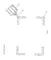
- Figures 1a and 1b show a loading station 100 for loading a carrier 1.
- Electronic components 11, for example, IC chips, that are to be tested by some testing device to which they can be transferred by means of the shown example of the inventive carrier 1, are to be secured on the carrier 1.
- the carrier 1 can be in an opened state wherein the electronic components are to be inserted or are inserted but not secured or in a clamped (locked, secured) state wherein the electronic components are inserted and secured. Opening and closing of the carrier 1 is caused by an opener 200.
- the opener 200 may comprise an actuating bolt 201 operating on a bevelled corner of the carrier 1.
- FIG 2a an exploded view of an embodiment of an inventive (clamping) carrier 1 for electronic components 11 is shown.
- the carrier 1 comprises a base plate 2 and a clamping plate (actuator) 3.
- the clamping plate 3 is moveable with respect to the base plate 2.
- the base plate 2 comprises a plurality of pockets 4.
- the pockets 4 of the base plate 2 can have a substantially rectangular form and can be structured pockets 4 that comprise plateau or mesa regions on which the electronic components can rest.
- the clamping plate 3 comprises a plurality of openings 5 corresponding to the pockets 4 of the base plate 2.
- elastic means 6 are provided for contacting the electronic components 11.
- the elastic means 6 may be provided in form of two polymeric lips arranged at edges of the openings 5.
- the elastic means 6 are provided for accounting for tolerances.
- Transition of the carrier 1 from an opened stated to a clamped state and vice versa is achieved by relative movement of the clamping plate 3 with respect to the base plate 2.
- This movement in the shown example, is guided by guiding pins 7 formed in the base plate 2 and corresponding long holes 8 formed in the clamping plate 3.
- diagonal movement of the rectangular clamping plate 3 with respect to the rectangular base plate 2 can be caused by the opener 200 shown in Figures 1a and 1b .
- the clamped state (shown in Figure 2a ) can be secured by a leaf spring 9 or any other means known in the art and at least provided at one edge of the base plate 2.
- the electronic components 11 are secured between the elastic means 6 of the openings 5 of the clamping plate 3 and edges of the pockets 4 of the base plate 2 that function as dead stops in the clamped state.
- the carrier 1 is transitioned from the clamped state ( Figure 2b ) to the opened state ( Figure 2c ) due to the corresponding movement of the clamping plate 2 with respect to the base plate 2 guided by the guiding pins 7 and long holes 8.
- the elastic means 6 no longer contact the electronic components 11 and the electronic components 11 can be removed from the carrier 1.
- the inventive carrier 1 exhibits a much more reliable and simpler construction as compared to the art.
- FIG 2d a carrier similar to the one shown in Figures 2a to 2c is illustrated.
- another clamping plate 3' is provided in addition to clamping plate 3.
- the two clamping plates 3 and 3' stacked over each other are moveable with respect to the base plate 2 for transition between the opened and clamped states.
- Both plates comprise opening and elastic means 6 and 6', respectively, provided at edges of the openings. Moreover, they are moveable with respect to each other and in different directions with respect to the first plate.
- the clamping plate 3 is moveable in the longitudinal direction with respect to the base plate 2 and the clamping layer 3' is moveable in the latitudinal direction with respect to the base plate 2.
- the electronic components 11 are secured by both clamping plates 3 and 3'.
- the clamping plate 3 may be operated by a first opener 200 and the clamping plate 3' may be operated by a second opener 200' different from the first one.
- Figures 2e and 2f show top views of the carrier with the first clamping plate 3 and both the first and second clamping plates 3 and 3', respectively.
- the first and second clamping plates 3 and 3' are secured to respective leaf springs 9 and 9'.
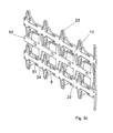
- FIG. 3a , 3b and 3c An alternative embodiment of the present invention is illustrated in Figures 3a , 3b and 3c .
- the shown embodiment may comprise a base plate or cover plate comprising an element (securing element) 50 with dead stops 10 formed as integral parts of the same or mounted thereon.
- the dead stops 10 are provided for securing electronic components 11 in the clamped state.
- the actuators 21 comprise clamping elements 16 arranged along linear guiding elements 22 that extend parallel to the rows of electronic components 11, spring elements 23 and stoppers 24. Moreover, an opening element 25 is provided at the end of a linear guiding element 22 that may or may not be integrally formed with the linear guiding element 22. The opening element is operated by opener 200.
- the linear guiding elements 22 and the clamping elements 16 may be integrally formed. Particularly, the clamping elements 16 and the linear guiding elements 22 may be etched from a stainless steel plate, for example, from stainless steel sheet with a thickness of about 0.2 mm. It is to be understood that the number of actuators 21 for the carrier 1, in principle, can be chosen arbitrarily.
- the electronic components 11 are inserted in the carrier loosely contacting the dead stops 10 of the element 50 that may be formed on a base plate.
- the electronic components 11 are not contacted by the clamping elements 16.
- the opening elements 25 may be realized by pre-loaded spring and the opened state is maintained by the opener 200 acting against the spring force of the preloaded springs.
- the opener 200 may mechanically act on the opening element 25 by means of an actuating bolt 201.
- the guiding extensions 51 are moved outwardly leaving some more space in the respective guiding slots 52 and restricted, if need by, by complementary stoppers 24'.
- the complementary stoppers 24' are provided for preventing damages in the clamped state that otherwise could be caused by contaminated electronic components 11 or individual electronic components 11 of inappropriate dimensions.
- the springs 23 are only provided to account for tolerances. They might be omitted, if the clamping elements 16 are formed of a material that allows for some deformation sufficient to compensate for tolerances, for example, of the sizes of possible contaminated electronic components 11 and/or inaccuracies of the movement and constructional details or wear of the actuator 21 (linear guiding element 22) and/or the clamping elements 16.
- FIG. 3c A close-up of the embodiment illustrated in Figures 3a and 3b is shown in Figure 3c . Particularly, it can be seen from Figure 3c that the thicknesses of the linear guiding elements 22, wedge-type clamping elements 16, stoppers 24 and 25' and spring elements 23 are the same in the shown example.
- the electronic components 11 are at most as thick as the elements 22, 6, 24, 23 and the securing element 50 in order to guarantee secure fastening of the electronic components 11.
- Figure 4a shows an exploded view of another exemplary embodiment of the invention.
- the carrier 1 shown in Figure 4a comprises a base plate 30 and a clamping plate 31 as an actuator in the sense of the present invention and a cover plate that in the shown example comprise a lower part 32 and an upper part 33.
- electronic components 11 can be introduced.
- the clamping plate 31 comprises springs 34, bands (cords) 35, deflection elements 36, for example, deflection balls, and openings 37 for accommodating electronic components 11. It may be preferred to provide both the upper and the lower side of the clamping plate 31 or only of these sides with corresponding springs 34, bands (cords) 35 and deflection elements 36.
- the cover plate comprises openings 38 corresponding to the openings 37 of the clamping plate 31.
- pockets are provided in the base plate 30 and, in this case, the clamping plate 31 comprises openings corresponding to the pockets of the base plate 30. The clamping plate 31 is moveable with respect to the base plate 30.
- a movable locking bar 39 is used for bringing the carrier 1 into a clamped state wherein the inserted electronic components 11 are secured.
- the movable locking bar 39 is removed from the bearing 40 provided in the base plate 30.
- electronic components 11 are inserted in the openings 37 in an opened state of the carrier 1.
- the springs 34 cause some pre-tensioning of the bands 35.
- the locking bar 39 is used for bringing the carrier 1 into a clamped state.
- the locking bar is moved into the bearing 40. Thereby, the clamping plate 31 is moved toward the lower edge of the base plate 30.
- the movement of the clamping plate 31 is, for example, guided by guiding pins moving along corresponding long holes formed in the base plate 30.
- the carrier 1 shown in Figures 4a and 4d comprises cut-outs 41 at the lower edge for accepting the lower edges of the electronic components 11 of the lowest row of electronic components 11 to be carried by the carrier 1.
- the electronic components 11 of the lowest row of electronic components 11 can be secured by means of the cut-outs 41 only or additionally by respective dead stops provided in the lower part 32 and/or upper part 33 of the cover plate (confer Figure 4a ).
- the electronic components 11 During movement of the clamping plate 31 for transitioning the carrier 1 from the opened state to the clamped state the electronic components 11 have to be fixed with respect to the bottom plate 30 and/or lower part 32 and/or upper part 33 of the cover plate in order to exert a mechanical force on the electronic components 11 by means of the clamping plate 31. In other words, the clamping plate 31 is moved with respect to the electronic components 11.
- the electronic components 11 can be fixed during the movement by (edges) of pockets (not shown in Figures 4a to 4d ) provided in the base plate 30 and/or edges of openings provided in the cover sheet.
- the electronic components 11 are thick enough that different stacked plates can interact with the electronic components 11. For example, the electronic components 11 have thicknesses of some 1 mm and the plates of some 0.2 mm.
- Figure 4d shows the carrier 1 in the clamped state wherein the locking bar 34 is completely inserted into the bearing 40 of the base plate 30. Edges of the openings 37 of the clamping plate 31 and/or the bands 35 exert mechanical forces on the respective upper right corners of the electronic components 11.
- the electronic components 11 are secured by the clamping plate 31 in interaction with corresponding dead stops provided in the lower part 32 and/or upper part 33 of the cover plate or corresponding pockets formed in the base plate 30, for example.
- the springs 34 are loaded and thereby exert a counterforce on the bands. The interaction of the springs 34 and bands 35 allow for fine adjustment and compensation for tolerances.
- the deflection elements 36 of the clamping plate 31 are arranged such that due to the deflection caused by them the bands 35 are tightened and the tightened bands 35 help keeping the electronic components 11 in place.
- This effect according to a particular example, is shown in detail in Figure 6 .
- An electronic component 11 is secured by band 35 guided by deflection elements 36 and an L-shaped dead stop 41, for example, formed by the edge of a pocket or opening provided in the base plate 30 and/or cover plate, respectively.
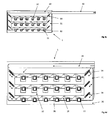
- FIG. 5a to 5c Another example of a carrier 1 is illustrated in Figures 5a to 5c wherein clamping of the electronic components 11 is also facilitated by means of bands.
- Figures 5a to 5c show a plate 60 comprising pockets or seats 61 for accommodating and securing the electronic components 11 and three actuators 62. Whereas three actuators 62 are shown, the number of actuators may be chosen differently.
- the plate 60 comprises cut-outs 43 at the lower edge for accepting the lower edges of the electronic components 11 of the lowest row of electronic components 11 to be carried by the carrier. In the clamped state of the carrier the electronic components 11 of the lowest row of electronic components 11 can be secured by means of the cut-outs 63.
- FIG. 6 is also an illustration of securing an electronic component for this example but one the deflection elements 35 shown in Figure 6 is formed on the plate 60 whereas the other one is formed on the bar actuator 62 in this embodiment.
- the actuators 62 are formed are bars that are moveable in bearings 67 of the plate 60. It is to be noted that the actuators 62 can be operated by corresponding openers associated with each of the actuators (not shown in Figures 5a to 5c ) or one single opener. Whereas in the previous example (see Figures 4a to 4d ) one actuator, namely the clamping plate 31, was moved for transition from the clamped state of the carrier to the opened state of the carrier and vice versa, in the embodiment shown in Figures 5 to 5c , three actuators 62 are moved.
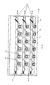
- the actuators 62 are almost completely inserted in the bearings 67 (i.e. almost up to the left-hand ends of the bearings 67 illustrated in Figure 5b ).
- the deflection elements 66' that are formed on or integrally with the actuators 62 cause tensioning of the bands 65 such that the electronic components 11 are secured against dead stops of the pockets 61 of the plate 60 and the cut-outs 63, respectively (see Figure 5b ).
- the actuators 62 may be pushed and secured against some springs 68 provided in the bearings 67, for example.
- the actuators 62 may be released and pushed outwardly of the bearings 67 by the springs 68 in order to cause transition of the carrier to the opened state (see Figure 5c ). In the opened state the bands 65 no longer contact the electronic components 11 and the electronic components 11 can be removed.
- a small number (one or more) of actuators is employed for transition of the carrier between the clamped and opened state and, moreover, a small number (one or more) of openers is needed for operating the actuators.
- the actuators are realized as plates or bars that can easily and inexpensively be manufactures and promise long lifetimes. Whereas mainly actuators are shown that are moveable in the same direction, all of the above-described exampled may be supplemented by additional actuators, for example, comprising additional clamping plates or linear guiding elements or bars, that are moveable in another direction, for example, in a direction perpendicular to the one of the shown examples.
Abstract
Description
- The present invention relates to a carrier for holding, transferring and aligning batches of individual electronic components (semiconductor devices).
- Electronic components, for example IC chips or Ball Grid Arrays, need to be tested after having been manufactured in a mass production process. The electronic components are tested as strip-shaped composites or as individual components usually grouped in batches. Testing of strip-shaped composites is not considered in the present invention. The batches are moved by some transfer element into a test position. At the test position the electrical terminals of the electronic components of the batch are contacted with some testing head of a testing device. Predetermined tests for particular electronic characteristics of the electronic components of the batch are performed by means of the testing head.
- In order to simultaneously test a plurality of electronic components of a batch a plurality of electrical contacts have to be provided in the testing head and highly accurate alignment of the electrical contacts of the testing header and the electrical terminals of the individual electronic components of the batch under investigation has to be ensured. In the art, it is known to accommodate individual electronic components in individual receiving pockets of a carrier and transfer the carrier to a testing head where electrical contact is made with the individual electronic components for testing purposes. The carrier, for example, comprises spring elements and stop elements for securing the individual electronic components in the individual receiving pockets (
US 7 258 703 andUS 2010/0206768 A1 ). - However, the known conventional securing mechanisms suffer from complicated and expensive constructions. In particular, relatively large spring elements are needed in the art for providing the clamping force for each electronic component. Such spring elements heavily suffer from ageing and restrict the density of receiving pockets and, thus, the number of the individual electronic components that are to be tested. Moreover, the reliability of the fastening of the individual electronic components that are to be transferred and tested should be improved. Therefore, it is an object of the present invention to provide means for holding, transferring and aligning batches of individual electronic components (semiconductor devices), particularly, for testing purposes that overcome the abovementioned problems.
- The above-mentioned object is addressed by the carrier for carrying a plurality of electronic components according to
claim 1. This carrier comprises
a first plate comprising a plurality of seats or openings each configured to accommodate one of the plurality of electronic components; and
a first actuator moveable in a first direction with respect to the first plate for securing more than one of the plurality of electronic components in the seats or openings in a clamped state of the carrier. - In this document, the term "seat" is to be understood broadly as a means for positioning the electronic components. In particular, the seats may comprise dead stops or edges at which the electronic components are secured in the clamped state of the carrier. Moreover, the seats may be recessed in the first plate or may protrude from the first plate. The first plate may have one or more elements mounted thereon or formed integrally therewith and the seats may be parts of the element(s) mounted on the first plate. The electronic components can be of rectangular shape and, thus, the seats and openings can also be of rectangular shape.
- In an opened state of the carrier the electronic components can be inserted. For securing the electronic components the first actuator is moved thereby clamping the electronic components in a clamped (secured, locked) state of the carrier. The first actuator represents a mechanical means, for example, a structured plate or a bar, that exerts a mechanical force on the clamped electronic components. In the art, for each of the electronic components one or more actuators in the form of springs are needed (see description above). In the present invention, by one actuator that is not made of a spring a plurality of electronic components are secured in the clamped state of the carrier. A subset or all of the electronic components may be secured by operation of the first actuator. If not all of the electronic components are secured by the first actuator one or more additional actuators are provided for securing the remaining electronic components that are not secured by the first actuator. For example, the first actuator may be provided for securing half of the number of the electronic components handled by means of the carrier and a second actuator is provided for securing the other half. One actuator may be provided for securing one or two rows of electronic components and one or more other actuators may be provided for securing the other rows of the batch of electronic components.
- Since there is no longer a need for providing one or more springs as actuators for each individual electronic component, the density of electronic components on the carrier can be increased. Moreover, the single mechanical actuator for securing a number of electronic components shows an increased durability as compared to the above-described spring actuators of the art. Safe transfer to and alignment with a testing header of a testing device can be guaranteed. Moreover, the carrier can be produced at relatively low costs due to the relatively simple construction.
- The first actuator can be opened by a single opener for moving the actuator and the carrier from the clamped state into the opened state. Different from the art there is no need for an individual opener provided for each of the plurality of electronic components. In fact, there may be more than one actuator each being operated by an individual single opener in the inventive carrier. However, the number of actuators and openers of the inventive carrier is less than the number of electronic components to be handled by means of the carrier.
- The first actuator may be configured to contact the electronic components by elastic means. The elasticity of the deformable elastic means allows for providing some tolerances with respect to the actual dimensions of the electronic components and possible contaminations of the electronic components. The elastic means may be realized in the form of polymeric means like polymeric lips or knobs.
- According to an embodiment the first plate is a base plate and the seats are formed as receiving pockets. In the opened state of the carrier the electronic components are inserted in the pockets of the base plate and at least a subset of the electronic components is secured in the pockets by means of the first actuator. In this case, the first actuator can comprise a clamping plate with a plurality of openings corresponding to the plurality of pockets of the base plate and is moveable with respect to the base plate. The pockets can be of substantially rectangular shape and, in this case, the clamping plate can be moveable to exert for each pocket a mechanical force along a diagonal of the rectangle defined by the pocket, particularly, only along a diagonal of the rectangle defined by the pocket. The pockets of the base plates can comprise plateau or mesa regions on which the electronic components can rest. When inserted the pockets the electronic components partially protrude from the pockets such that they can get into contact with the edges of the openings of the clamping plate.
- Both the clamping plate and the first plate can be of rectangular shape and the directions of forces exerted on the electronic components can be substantially parallel to a diagonal of the first/clamping plate. Insertion of the electronic components into the pockets is performed in an opened state of the carrier. In the opened state enough space is provided in the pockets to insert the electronic components. For securing the electronic components the clamping plate is moved parallel and in a predetermined angle with respect to a longitudinal axis of the base plate thereby clamping the electronic components between edges of the pockets of the base plate and the corresponding openings of the clamping plate. The edges of the openings can be provided with elastic means for contacting the electronic components in the clamped state.
- It is to be noted that in the clamped state the actuator (for example, realized by or comprising a clamping plate) and the first plate can be secured to each other by any means known in the art, for example, by one or more leaf springs provided at one or more edges of the first plate.
- According to another embodiment, the first plate comprises an elongated element comprising dead stops for receiving edges of the electronic components in the clamped state. The first actuator comprises a plurality of clamping elements arranged along a straight line and configured for securing the electronic components in the clamped state. The clamping elements directly contact the electronic components for clamping. In principle, the clamping elements may be made of any suitable form and may exert a mechanical force (at some predetermined angle) on one or two edges or a corner of an electronic component.
- The first actuator may comprise a linear guiding element with a longitudinal axis and the clamping elements can be formed as wedges, in particular, in the shape of right-angled triangles, on both sides of the linear guiding element. One edge of each of the wedges contacts a corner of one of the electronic components for securing it safely to a corresponding dead stop of the elongated element. The clamping elements can be grouped in pairs and, in this case, one clamping element of a pair of clamping elements is arranged on one side of a linear guiding element and the other clamping element of the pair of clamping elements is arranged on the other side of the linear guiding element symmetrically to the linear guiding element. In this embodiment, the electronic components can be arranged in rows parallel to the longitudinal axis of the linear guiding element and in the clamped state one clamping element of each pair of clamping elements can be operable to exert the mechanical force on an electronic component of one row and, in this case, the other clamping element of each pair of clamping elements is operable to exert the mechanical force on another electronic component of another row (neighboured and arranged parallel to the first mentioned row).
- In the opened state of the carrier according to this embodiment the electronic components can be inserted at or close to the dead stops of the elongated element of the first plate and without contact with the edges of the wedges. The opened state is achieved by pushing the first actuator (linear guiding element) by means of a single opener acting on some opening element of the actuator (the opening element may be part of or attached to the guiding element). The linear guiding element is movable to exert a mechanical force on the corner of the rectangular electronic component when accommodated in a pocket by the hypotenuse edge of the wedge (triangle).
- According to an example, a wedge shaped clamping element or a pair of wedge shaped clamping elements arranged symmetrically on both sides of a linear guiding element that connects pairs of clamping elements along a main longitudinal axis of the rectangular clamping plate is directly connected to a spring element. The spring element can be formed as a (pre-loaded) leaf spring. The spring, in this example, is provided in order to compensate for non-uniformity of the electronic components, i.e. it provides for some tolerance and fine adjustment of the mechanical force exerted on the electronic component. It is important to note that the main clamping force is provided by the actuator and clamping elements and that the springs are just provided for compensation purposes. These compensation purposes can, alternatively, by provided by making the clamping elements of some sufficiently resilient (deformable) material allowing for some deformation of the clamping elements in the clamped state.
- Moreover, it may be preferable to provide for each of the clamping elements first and second stops formed on the linear guiding element and arranged for restricting movement of the clamping elements along the longitudinal axis of the linear guiding element. The first stop restricts the movement of the clamping elements during transition of the carrier from the opened state to the clamped state and the second stop restricts the movement of the clamping elements during transition of the carrier from the clamped state to the opened state.
- According to another example, the carrier may further comprise a second actuator comprising another linear guiding element and the clamping elements formed on both sides of the other linear guiding element, in particular, in the form of wedges. The first and second actuators are arranged parallel to each other and each of the actuators can be opened by a corresponding opener separately from each other. Securement and release or insertion of the electronic components can, thus, be carried out for different pair of rows of electronic components separately, for example.
- According to an alternative embodiment the first actuator comprises a clamping plate comprising bands and springs. In this embodiment, the electronic components are secured in the clamped state of the carrier by means of elastic bands representing the above-mentioned elastic means. In this embodiment, deflection elements, for example, deflection balls, are provided to facilitate tightening the elastic bands by respective springs. Thereby, the electronic components are secured in the pockets. In the opened state of the carrier the bands are pre-tensioned by the springs. Only one surface or both main surfaces (top and bottom surface) of the clamping plate can be provided with the bands, deflection elements and spring elements. According to a particular example, multiple rows of pockets or openings are arranged in the first plate and multiple rows of openings are arranged in the clamping plate and one band is arranged for one row to exert force on the electronic components of the row in a clamped state and at the beginning of the row and at the end of the row a spring element is respectively arranged for tightening the band. On both sides of the row, i.e. at the beginning of the row and at the end of the row, a spring element is arranged for tightening the band. In this example, such a configuration can be provided for each of the rows of pockets (see also detailed description below).
- The first plate may be a base plate that comprises a bearing provided along an edge of the same and, in this case, in the clamped state the carrier comprises a locking bar introduced in the bearing. By introducing the locking bar the clamping plate arranged on the first plate is moved in the clamped position. The base plate may have pockets for accommodating the electronic components. In the clamped state the bands may be arranged to secure the electronic components against edges of these pockets.
- According to another example, the clamping plate is arranged on a bottom plate and the first plate is arranged above the clamping plate and comprises openings for the electronic components. In this case, in the clamped state the bands may be arranged to secure the electronic components against edges of the openings of the first plate.
- In again another example, the electronic components are also secured by bands. In this example, the first plate or a second plate comprises openings for the electronic components, bands and deflection elements comparable to the example described above. The first actuator is realized as a movable bar that can be moved in a corresponding bearing of the first or second plate. Alternatively, the moveable bar may comprise guiding pins extending through and guided in corresponding guiding holes provided in the first plate or the second plate, respectively. Moreover, the bar comprises deflection elements. The bands are guided by the deflection elements of the plate and the deflection elements of the bar such that in the clamped state of the carrier the bands exert clamping forces on the electronic components. By operation of an opener the first actuator is moved such that the deflection elements of the actuator (bar) do no longer provide tension of the bands that results in the clamping forces on the electronic components. Rows of electronic components can be secured individually by providing individual bars each comprising deflection elements, for example, one bar for each row (in this case, the number of actuators and openers equals the number of rows of electronic components; on the other hand, if it is considered appropriate, more than one of the bar actuators may be opened by the same opener). Similar to the example described above the springs formed on the plate are provided for pre-tensioning the bands.
- In all of the above-described examples, the first actuator is movable for securing or releasing the electronic components. One or more second actuators may be additionally provided that are operable subsequently in parallel to operation of the first actuator. The directions of movements of the actuators may be parallel to each other. Thereby, for example, individual rows of electronic components can be dealt with separately. However, it might also be considered appropriate to provide a second actuator that is movable in a second direction different from the first direction of movement of the first actuator (for example, perpendicular to the first direction) in order to further secure the electronic components by exerting mechanical forces in a direction different from the one of the forces exerted by the first actuator. For example, by the first actuator the electronic components are pressed against ones of the edges of the opening or seats of the first plate accommodating the electronic components and by the second actuator the electronic components are pressed against other ones of the edges of the opening or seats of the first plate accommodating the electronic components. The first and second actuators can be arranged in different planes on the same side or on different sides of the first plate.
- The first actuator may comprise or consist of a second plate and the second actuator may comprise or consists of a third plate and, in this case, the second and third plates are moveable with respect to each other and in different directions with respect to the first plate. For example, the first actuator (second plate) may be moveable in the longitudinal direction (y-direction) and the second actuator (third plate) can be moveable in the latitudinal direction (x-direction). The first plate, in this embodiment, can be a base plate comprising one or two metal sheets or may be provided as a milled part. Moreover, the carrier may comprise a cover sheet above the second and third plate that are both provided above the base plate in this embodiment and the cover plate and the base plate are fixed to each other. In the clamped state the first and second actuator are secured against the base plate by any means known in the art, for example, leaf springs.
- Further features and advantages of the present invention will be described in the following with reference to the figures, which illustrate only examples of embodiments of the present invention. The illustrated and described features may be suitably combined with each other.
-
Figures 1a and1b show a loading station for loading a carrier and an opener. -
Figures 2a ,2b and2c show, respectively, an exploded view and plan views of an example of a carrier according to the invention wherein the carrier comprises pockets for accommodating electronic components and a clamping plate for securing the electronic components. -
Figures 2d to 2f show a carrier similar to the one shown inFigures 2a to 2c but comprising an additional clamping plate. -
Figures 3a ,3b and3c illustrate another example of an inventive carrier wherein clamping elements in form of wedge elements are provided for securing electronic components. -
Figures 4a to 4d illustrate another example of an inventive carrier wherein electronic components are secured by means of bands. -
Figures 5a to 5c illustrate another example of an inventive carrier wherein electronic components are secured by means of bands. -
Figure 6 illustrates in a detailed view securing of an electronic component in the embodiment shown inFigures 4a to 5c . -
Figures 1a and1b show aloading station 100 for loading acarrier 1.Electronic components 11, for example, IC chips, that are to be tested by some testing device to which they can be transferred by means of the shown example of theinventive carrier 1, are to be secured on thecarrier 1. Thecarrier 1 can be in an opened state wherein the electronic components are to be inserted or are inserted but not secured or in a clamped (locked, secured) state wherein the electronic components are inserted and secured. Opening and closing of thecarrier 1 is caused by anopener 200. Theopener 200 may comprise anactuating bolt 201 operating on a bevelled corner of thecarrier 1. - In
Figure 2a an exploded view of an embodiment of an inventive (clamping)carrier 1 forelectronic components 11 is shown. InFigure 2b a clamped state of thecarrier 1 shown inFigure 2a is illustrated and inFigure 2c an opened state of thecarrier 1 shown inFigure 2a is illustrated. Thecarrier 1 comprises abase plate 2 and a clamping plate (actuator) 3. The clampingplate 3 is moveable with respect to thebase plate 2. Thebase plate 2 comprises a plurality of pockets 4. The pockets 4 of thebase plate 2 can have a substantially rectangular form and can be structured pockets 4 that comprise plateau or mesa regions on which the electronic components can rest.The clampingplate 3 comprises a plurality of openings 5 corresponding to the pockets 4 of thebase plate 2. For each of the pockets 5elastic means 6 are provided for contacting theelectronic components 11. The elastic means 6 may be provided in form of two polymeric lips arranged at edges of the openings 5. The elastic means 6 are provided for accounting for tolerances. - Transition of the
carrier 1 from an opened stated to a clamped state and vice versa is achieved by relative movement of theclamping plate 3 with respect to thebase plate 2. This movement, in the shown example, is guided by guidingpins 7 formed in thebase plate 2 and corresponding long holes 8 formed in theclamping plate 3. In the shown example, diagonal movement of therectangular clamping plate 3 with respect to therectangular base plate 2 can be caused by theopener 200 shown inFigures 1a and1b . In this and all other examples, the clamped state (shown inFigure 2a ) can be secured by aleaf spring 9 or any other means known in the art and at least provided at one edge of thebase plate 2. In the clamped state theelectronic components 11 are secured between theelastic means 6 of the openings 5 of theclamping plate 3 and edges of the pockets 4 of thebase plate 2 that function as dead stops in the clamped state. By pushing the clampedplate 3 at the bevelled corner of thecarrier 1 by theopener 200 againstleaf spring 9, thecarrier 1 is transitioned from the clamped state (Figure 2b ) to the opened state (Figure 2c ) due to the corresponding movement of theclamping plate 2 with respect to thebase plate 2 guided by the guiding pins 7 and long holes 8. In the opened state theelastic means 6 no longer contact theelectronic components 11 and theelectronic components 11 can be removed from thecarrier 1. - As illustrated in
Figures 2a to 2c only onesingle opener 200 is needed for operating the single actuator realized in form of theclamping plate 3 securing the electronic components in the clamped state. Theopener 200, in principle, can be arranged to act along an arbitrarily preselected line of force, for example, in a diagonal or longitudinal direction of thecarrier 1. No individual springs are needed as individual actuators exerting forces on individual electronic components and to be operated by individual openers as it is the case in the art. Thus, theinventive carrier 1 exhibits a much more reliable and simpler construction as compared to the art. - In
Figure 2d a carrier similar to the one shown inFigures 2a to 2c is illustrated. In this example, however, another clamping plate 3' is provided in addition to clampingplate 3. The twoclamping plates 3 and 3' stacked over each other are moveable with respect to thebase plate 2 for transition between the opened and clamped states. Both plates comprise opening andelastic means 6 and 6', respectively, provided at edges of the openings. Moreover, they are moveable with respect to each other and in different directions with respect to the first plate. In the shown example, the clampingplate 3 is moveable in the longitudinal direction with respect to thebase plate 2 and the clamping layer 3' is moveable in the latitudinal direction with respect to thebase plate 2. In the clamped state, theelectronic components 11 are secured by both clampingplates 3 and 3'. The clampingplate 3 may be operated by afirst opener 200 and the clamping plate 3' may be operated by a second opener 200' different from the first one.Figures 2e and2f show top views of the carrier with thefirst clamping plate 3 and both the first andsecond clamping plates 3 and 3', respectively. The first andsecond clamping plates 3 and 3' are secured torespective leaf springs 9 and 9'. - An alternative embodiment of the present invention is illustrated in
Figures 3a ,3b and3c . The shown embodiment may comprise a base plate or cover plate comprising an element (securing element) 50 withdead stops 10 formed as integral parts of the same or mounted thereon. The dead stops 10 are provided for securingelectronic components 11 in the clamped state. - The
actuators 21 comprise clampingelements 16 arranged along linear guidingelements 22 that extend parallel to the rows ofelectronic components 11,spring elements 23 andstoppers 24. Moreover, anopening element 25 is provided at the end of a linear guidingelement 22 that may or may not be integrally formed with the linear guidingelement 22. The opening element is operated byopener 200. Thelinear guiding elements 22 and theclamping elements 16 may be integrally formed. Particularly, the clampingelements 16 and thelinear guiding elements 22 may be etched from a stainless steel plate, for example, from stainless steel sheet with a thickness of about 0.2 mm. It is to be understood that the number ofactuators 21 for thecarrier 1, in principle, can be chosen arbitrarily. - In the opened state shown in
Figure 3a theelectronic components 11 are inserted in the carrier loosely contacting the dead stops 10 of theelement 50 that may be formed on a base plate. In the opened state of the carrier theelectronic components 11 are not contacted by the clamping elements 16.The openingelements 25 may be realized by pre-loaded spring and the opened state is maintained by theopener 200 acting against the spring force of the preloaded springs. Theopener 200 may mechanically act on theopening element 25 by means of anactuating bolt 201. - When the
opener 200 moves theactuating bolt 201 away from theopening element 25 transition to the clamped state (Figure 3b ) of the carrier is achieved. In the clamped state theelectronic components 11 are secured to the dead stops 10 by the clampingelements 16. By actuating oneactuator 21 by one opener 200 a number ofelectronic components 11 arranged in two rows (operated by pairs of clampingelements 16 arranged on both sides of the respective linear guiding element 22) are secured or released. The wedge-type clamping elements 16 have guidingextensions 51 that, in the opened state of the carrier (Figure 3a ), are inserted inrespective guiding slots 52 restricted bystoppers 24. In the clamped state (Figure 3b ) the guidingextensions 51 are moved outwardly leaving some more space in therespective guiding slots 52 and restricted, if need by, by complementary stoppers 24'. The complementary stoppers 24' are provided for preventing damages in the clamped state that otherwise could be caused by contaminatedelectronic components 11 or individualelectronic components 11 of inappropriate dimensions. - The
springs 23 are only provided to account for tolerances. They might be omitted, if theclamping elements 16 are formed of a material that allows for some deformation sufficient to compensate for tolerances, for example, of the sizes of possible contaminatedelectronic components 11 and/or inaccuracies of the movement and constructional details or wear of the actuator 21 (linear guiding element 22) and/or theclamping elements 16. - A close-up of the embodiment illustrated in
Figures 3a and3b is shown inFigure 3c . Particularly, it can be seen fromFigure 3c that the thicknesses of thelinear guiding elements 22, wedge-type clamping elements 16,stoppers 24 and 25' andspring elements 23 are the same in the shown example. Theelectronic components 11 are at most as thick as theelements element 50 in order to guarantee secure fastening of theelectronic components 11. -
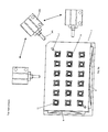
Figure 4a shows an exploded view of another exemplary embodiment of the invention. Thecarrier 1 shown inFigure 4a comprises abase plate 30 and a clampingplate 31 as an actuator in the sense of the present invention and a cover plate that in the shown example comprise alower part 32 and anupper part 33. In an opened state of thecarrier 1,electronic components 11 can be introduced. - The clamping
plate 31 comprisessprings 34, bands (cords) 35,deflection elements 36, for example, deflection balls, andopenings 37 for accommodatingelectronic components 11. It may be preferred to provide both the upper and the lower side of the clampingplate 31 or only of these sides withcorresponding springs 34, bands (cords) 35 anddeflection elements 36. The cover plate comprisesopenings 38 corresponding to theopenings 37 of the clampingplate 31. According to another example, pockets are provided in thebase plate 30 and, in this case, the clampingplate 31 comprises openings corresponding to the pockets of thebase plate 30. The clampingplate 31 is moveable with respect to thebase plate 30. - Also shown in
Figure 4a amovable locking bar 39 is used for bringing thecarrier 1 into a clamped state wherein the insertedelectronic components 11 are secured. In the opened state themovable locking bar 39 is removed from the bearing 40 provided in thebase plate 30. As shown inFigure 4b electronic components 11 are inserted in theopenings 37 in an opened state of thecarrier 1. In the opened state (Figures 4b and4c ) thesprings 34 cause some pre-tensioning of thebands 35. After theelectronic components 11 are inserted in theopenings 37 the lockingbar 39 is used for bringing thecarrier 1 into a clamped state. The locking bar is moved into thebearing 40. Thereby, the clampingplate 31 is moved toward the lower edge of thebase plate 30. The movement of the clampingplate 31 is, for example, guided by guiding pins moving along corresponding long holes formed in thebase plate 30. Thecarrier 1 shown inFigures 4a and4d comprises cut-outs 41 at the lower edge for accepting the lower edges of theelectronic components 11 of the lowest row ofelectronic components 11 to be carried by thecarrier 1. In the clamped state theelectronic components 11 of the lowest row ofelectronic components 11 can be secured by means of the cut-outs 41 only or additionally by respective dead stops provided in thelower part 32 and/orupper part 33 of the cover plate (conferFigure 4a ). - During movement of the clamping
plate 31 for transitioning thecarrier 1 from the opened state to the clamped state theelectronic components 11 have to be fixed with respect to thebottom plate 30 and/orlower part 32 and/orupper part 33 of the cover plate in order to exert a mechanical force on theelectronic components 11 by means of the clampingplate 31. In other words, the clampingplate 31 is moved with respect to theelectronic components 11. Theelectronic components 11 can be fixed during the movement by (edges) of pockets (not shown inFigures 4a to 4d ) provided in thebase plate 30 and/or edges of openings provided in the cover sheet. Theelectronic components 11 are thick enough that different stacked plates can interact with theelectronic components 11. For example, theelectronic components 11 have thicknesses of some 1 mm and the plates of some 0.2 mm. -
Figure 4d shows thecarrier 1 in the clamped state wherein the lockingbar 34 is completely inserted into the bearing 40 of thebase plate 30. Edges of theopenings 37 of the clampingplate 31 and/or thebands 35 exert mechanical forces on the respective upper right corners of theelectronic components 11. Theelectronic components 11 are secured by the clampingplate 31 in interaction with corresponding dead stops provided in thelower part 32 and/orupper part 33 of the cover plate or corresponding pockets formed in thebase plate 30, for example. Thesprings 34 are loaded and thereby exert a counterforce on the bands. The interaction of thesprings 34 andbands 35 allow for fine adjustment and compensation for tolerances. - The
deflection elements 36 of the clampingplate 31 are arranged such that due to the deflection caused by them thebands 35 are tightened and the tightenedbands 35 help keeping theelectronic components 11 in place. This effect, according to a particular example, is shown in detail inFigure 6 . Anelectronic component 11 is secured byband 35 guided bydeflection elements 36 and an L-shapeddead stop 41, for example, formed by the edge of a pocket or opening provided in thebase plate 30 and/or cover plate, respectively. - Another example of a
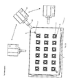
carrier 1 is illustrated inFigures 5a to 5c wherein clamping of theelectronic components 11 is also facilitated by means of bands.Figures 5a to 5c show aplate 60 comprising pockets orseats 61 for accommodating and securing theelectronic components 11 and threeactuators 62. Whereas threeactuators 62 are shown, the number of actuators may be chosen differently. Theplate 60 comprises cut-outs 43 at the lower edge for accepting the lower edges of theelectronic components 11 of the lowest row ofelectronic components 11 to be carried by the carrier. In the clamped state of the carrier theelectronic components 11 of the lowest row ofelectronic components 11 can be secured by means of the cut-outs 63. Similar to the example shown inFigures 4a to 4d there are providedsprings 64,bands 65 anddeflection elements 66 and 66'. However, one group ofdefection elements 66 is formed on theplate 60, whereas the other group of deflection elements 66' is formed as part of theactuators 62.Figure 6 is also an illustration of securing an electronic component for this example but one thedeflection elements 35 shown inFigure 6 is formed on theplate 60 whereas the other one is formed on thebar actuator 62 in this embodiment. - The
actuators 62 are formed are bars that are moveable in bearings 67 of theplate 60. It is to be noted that theactuators 62 can be operated by corresponding openers associated with each of the actuators (not shown inFigures 5a to 5c ) or one single opener. Whereas in the previous example (seeFigures 4a to 4d ) one actuator, namely the clampingplate 31, was moved for transition from the clamped state of the carrier to the opened state of the carrier and vice versa, in the embodiment shown inFigures 5 to 5c , threeactuators 62 are moved. - In the clamped state the
actuators 62 are almost completely inserted in the bearings 67 (i.e. almost up to the left-hand ends of the bearings 67 illustrated inFigure 5b ). In this position, the deflection elements 66' that are formed on or integrally with theactuators 62 cause tensioning of thebands 65 such that theelectronic components 11 are secured against dead stops of thepockets 61 of theplate 60 and the cut-outs 63, respectively (seeFigure 5b ). Theactuators 62 may be pushed and secured against somesprings 68 provided in the bearings 67, for example. - By operation of one or more openers the
actuators 62 may be released and pushed outwardly of the bearings 67 by thesprings 68 in order to cause transition of the carrier to the opened state (seeFigure 5c ). In the opened state thebands 65 no longer contact theelectronic components 11 and theelectronic components 11 can be removed. - In the all of the above-described embodiments a small number (one or more) of actuators is employed for transition of the carrier between the clamped and opened state and, moreover, a small number (one or more) of openers is needed for operating the actuators. The actuators are realized as plates or bars that can easily and inexpensively be manufactures and promise long lifetimes. Whereas mainly actuators are shown that are moveable in the same direction, all of the above-described exampled may be supplemented by additional actuators, for example, comprising additional clamping plates or linear guiding elements or bars, that are moveable in another direction, for example, in a direction perpendicular to the one of the shown examples.
Claims (15)
- Carrier for carrying a plurality of electronic components, comprising
a first plate comprising a plurality of seats or openings each configured to accommodate one of the plurality of electronic components; and
a first actuator moveable in a first direction with respect to the first plate for securing more than one of the plurality of electronic components in the seats or openings in a clamped state of the carrier. - The carrier according to claim 1, wherein the first actuator comprises elastic means for contacting the electronic components.
- The carrier according to one of the preceding claims, wherein the first plate is a base plate comprising a plurality of pockets each configured to accommodate one of the plurality of electronic components and the first actuator comprises a clamping plate comprising a plurality of openings corresponding to the plurality or pockets of the base plate.
- The carrier according to claim 1 or 2, wherein the first plate comprises an elongated element comprising dead stops for receiving edges of the electronic components in the clamped state and the first actuator comprises a plurality of clamping elements arranged along a straight line and configured for securing the electronic components in the clamped state.
- The carrier according to claim 4, wherein the first actuator comprises a linear guiding element and the clamping elements are formed on both sides of the linear guiding element, in particular, in the form of wedges.
- The carrier according to claim 5, wherein the clamping elements are grouped in pairs and one clamping element of a pair of clamping elements is arranged on one side of a linear guiding element and the other clamping element of the pair of clamping elements is arranged on the other side of the linear guiding element symmetrically to the linear guiding element.
- The carrier according to claim 5 or 6, wherein each of the clamping elements is connected with a corresponding spring being part of or connected with the linear guiding element and/or the clamping elements are made of a resilient material.
- The carrier according to one of the claims 5 to 7, further comprising a second actuator comprising another linear guiding element and the clamping elements formed on both sides of the other linear guiding element, in particular, in the form of wedges.
- The carrier according to claim 2, wherein the elastic means are elastic bands and the first actuator comprises a clamping plate comprising springs configured for pre-tensioning the bands in an opened state of the carrier and deflection elements for guiding the bands.
- The carrier according to claim 9, wherein multiple rows of pockets or openings are arranged in the first plate and multiple rows of openings are arranged in the clamping plate and one band is arranged for one row to exert force on the electronic components of the row in a clamped state and at the beginning of the row and at the end of the row a spring element is respectively arranged for tightening the band.
- The carrier according to one of the claims 9 or 10, further comprising a bottom plate arranged below the clamping plate and comprising a bearing provided along an edge of the same and wherein in a clamped state the carrier comprises a locking bar introduced in the bearing.
- The carrier according to one of the claims 9 to 11, wherein the first plate is arranged above the clamping plate and comprises openings corresponding to the electronic components and wherein in the clamped state of the carrier the electronic components are secured to edges of the openings.
- The carrier according to claim 1, wherein the first plate or an additionally provided second plate comprises openings for the electronic components, bands and first deflection elements and the first actuator comprises or consists of a movable bar comprising second deflection elements, in particular, such that in the clamped state the electronic components are secured by the bands guided by the first and second deflection elements and in an opened state the bands guided by the first and second deflection elements do not contact the electronic components.
- The carrier according to one of the preceding claims, further comprising a second actuator moveable with respect to the first plate and in a second direction different from the first direction, for example, perpendicular to the first direction, for securing more than one of the plurality of electronic components in the seats or openings in a clamped state of the carrier.
- The carrier according to claim 14, wherein the first actuator comprises a second plate and the second actuator comprises a third plate and wherein the second and third plates are moveable with respect to each other and in different directions with respect to the first plate.
Priority Applications (1)
| Application Number | Priority Date | Filing Date | Title |
|---|---|---|---|
| EP13154816.6A EP2765431B1 (en) | 2013-02-11 | 2013-02-11 | Carrier for electronic components |
Applications Claiming Priority (1)
| Application Number | Priority Date | Filing Date | Title |
|---|---|---|---|
| EP13154816.6A EP2765431B1 (en) | 2013-02-11 | 2013-02-11 | Carrier for electronic components |
Publications (2)
| Publication Number | Publication Date |
|---|---|
| EP2765431A1 true EP2765431A1 (en) | 2014-08-13 |
| EP2765431B1 EP2765431B1 (en) | 2016-05-25 |
Family
ID=47757321
Family Applications (1)
| Application Number | Title | Priority Date | Filing Date |
|---|---|---|---|
| EP13154816.6A Not-in-force EP2765431B1 (en) | 2013-02-11 | 2013-02-11 | Carrier for electronic components |
Country Status (1)
| Country | Link |
|---|---|
| EP (1) | EP2765431B1 (en) |
Cited By (3)
| Publication number | Priority date | Publication date | Assignee | Title |
|---|---|---|---|---|
| EP3007217A1 (en) * | 2014-10-10 | 2016-04-13 | Rasco GmbH | Chip tray |
| WO2017178364A1 (en) * | 2016-04-14 | 2017-10-19 | Muehlbauer GmbH & Co. KG | Device, system, and method for aligning electronic components |
| WO2021148281A1 (en) * | 2020-01-23 | 2021-07-29 | Lpkf Laser & Electronics Ag | Mounting method for an integrated semiconductor wafer device, and mounting device |
Citations (5)
| Publication number | Priority date | Publication date | Assignee | Title |
|---|---|---|---|---|
| JPH0373551A (en) * | 1989-08-15 | 1991-03-28 | Tokyo Electron Ltd | Chip tray |
| US20060154386A1 (en) * | 2005-01-07 | 2006-07-13 | Asm Assembly Automation Ltd. | Apparatus and method for aligning devices on carriers |
| US20070131733A1 (en) * | 2005-12-12 | 2007-06-14 | Asm Assembly Automation Ltd. | Apparatus and method for arranging devices for processing |
| US20100206768A1 (en) | 2008-02-15 | 2010-08-19 | Multitest Elektronische Systeme Gmbh | Device and method for aligning and holding a plurality of singulated semiconductor components in receiving pockets of a terminal carrier |
| EP2290375A2 (en) * | 2009-08-18 | 2011-03-02 | Multitest elektronische Systeme GmbH | Carrier for aligning electronic components with slidably arranged plates |
Family Cites Families (1)
| Publication number | Priority date | Publication date | Assignee | Title |
|---|---|---|---|---|
| JP2009096523A (en) * | 2007-10-17 | 2009-05-07 | Panasonic Corp | Carrier frame of electronic component and method for production of electronic component |
-
2013
- 2013-02-11 EP EP13154816.6A patent/EP2765431B1/en not_active Not-in-force
Patent Citations (6)
| Publication number | Priority date | Publication date | Assignee | Title |
|---|---|---|---|---|
| JPH0373551A (en) * | 1989-08-15 | 1991-03-28 | Tokyo Electron Ltd | Chip tray |
| US20060154386A1 (en) * | 2005-01-07 | 2006-07-13 | Asm Assembly Automation Ltd. | Apparatus and method for aligning devices on carriers |
| US7258703B2 (en) | 2005-01-07 | 2007-08-21 | Asm Assembly Automation Ltd. | Apparatus and method for aligning devices on carriers |
| US20070131733A1 (en) * | 2005-12-12 | 2007-06-14 | Asm Assembly Automation Ltd. | Apparatus and method for arranging devices for processing |
| US20100206768A1 (en) | 2008-02-15 | 2010-08-19 | Multitest Elektronische Systeme Gmbh | Device and method for aligning and holding a plurality of singulated semiconductor components in receiving pockets of a terminal carrier |
| EP2290375A2 (en) * | 2009-08-18 | 2011-03-02 | Multitest elektronische Systeme GmbH | Carrier for aligning electronic components with slidably arranged plates |
Cited By (5)
| Publication number | Priority date | Publication date | Assignee | Title |
|---|---|---|---|---|
| EP3007217A1 (en) * | 2014-10-10 | 2016-04-13 | Rasco GmbH | Chip tray |
| WO2016055583A1 (en) * | 2014-10-10 | 2016-04-14 | Rasco Gmbh | Chip tray |
| WO2017178364A1 (en) * | 2016-04-14 | 2017-10-19 | Muehlbauer GmbH & Co. KG | Device, system, and method for aligning electronic components |
| US10604358B2 (en) | 2016-04-14 | 2020-03-31 | Muehlbauer GmbH & Co. KG | Device, system and method for aligning electronic components |
| WO2021148281A1 (en) * | 2020-01-23 | 2021-07-29 | Lpkf Laser & Electronics Ag | Mounting method for an integrated semiconductor wafer device, and mounting device |
Also Published As
| Publication number | Publication date |
|---|---|
| EP2765431B1 (en) | 2016-05-25 |
Similar Documents
| Publication | Publication Date | Title |
|---|---|---|
| US10290526B2 (en) | Device and method for aligning and holding a plurality of singulated semiconductor components in receiving pockets of a terminal carrier | |
| US7210953B2 (en) | Socket for electrical parts | |
| US8230587B2 (en) | Carrier for aligning electronic components with slidably arranged plates | |
| US8689436B2 (en) | Two abutting sections of an align fixture together floatingly engaging an electronic component | |
| US8342872B2 (en) | Socket having two plates for holding contact pins and an urging member for urging the plates together | |
| EP2290374B1 (en) | Elastic unit exerting two angled force components on an abutting section of an align fixture | |
| US8964404B2 (en) | Elastic unit for clamping an electronic component and extending below an electronic component receiving volume of an align fixture | |
| EP2765431B1 (en) | Carrier for electronic components | |
| US8787035B2 (en) | Electrical interconnect device | |
| JP2018029040A (en) | Socket for electrical component | |
| US20170301575A1 (en) | Chip tray | |
| US20130171855A1 (en) | Socket for electric parts | |
| US11237207B2 (en) | Semiconductor test socket with a floating plate and latch for holding the semiconductor device | |
| EP2884293A1 (en) | Semiconductor device carrier | |
| JP4767741B2 (en) | Socket for electrical parts | |
| US20230038252A1 (en) | Socket | |
| US8888503B2 (en) | Socket for electric parts | |
| US20060094279A1 (en) | Socket for electrical parts | |
| JP4974710B2 (en) | socket | |
| KR20090008062A (en) | Opener and buffer table for test handler | |
| KR101652901B1 (en) | Side docking type test handler and pushing apparatus for test handler | |
| KR20100104668A (en) | Carrier module for test handler |
Legal Events
| Date | Code | Title | Description |
|---|---|---|---|
| PUAI | Public reference made under article 153(3) epc to a published international application that has entered the european phase |
Free format text: ORIGINAL CODE: 0009012 |
|
| 17P | Request for examination filed |
Effective date: 20131121 |
|
| AK | Designated contracting states |
Kind code of ref document: A1 Designated state(s): AL AT BE BG CH CY CZ DE DK EE ES FI FR GB GR HR HU IE IS IT LI LT LU LV MC MK MT NL NO PL PT RO RS SE SI SK SM TR |
|
| AX | Request for extension of the european patent |
Extension state: BA ME |
|
| GRAP | Despatch of communication of intention to grant a patent |
Free format text: ORIGINAL CODE: EPIDOSNIGR1 |
|
| INTG | Intention to grant announced |
Effective date: 20151209 |
|
| GRAS | Grant fee paid |
Free format text: ORIGINAL CODE: EPIDOSNIGR3 |
|
| GRAA | (expected) grant |
Free format text: ORIGINAL CODE: 0009210 |
|
| AK | Designated contracting states |
Kind code of ref document: B1 Designated state(s): AL AT BE BG CH CY CZ DE DK EE ES FI FR GB GR HR HU IE IS IT LI LT LU LV MC MK MT NL NO PL PT RO RS SE SI SK SM TR |
|
| REG | Reference to a national code |
Ref country code: GB Ref legal event code: FG4D |
|
| REG | Reference to a national code |
Ref country code: CH Ref legal event code: EP |
|
| REG | Reference to a national code |
Ref country code: IE Ref legal event code: FG4D Ref country code: AT Ref legal event code: REF Ref document number: 802731 Country of ref document: AT Kind code of ref document: T Effective date: 20160615 |
|
| REG | Reference to a national code |
Ref country code: DE Ref legal event code: R096 Ref document number: 602013007788 Country of ref document: DE |
|
| REG | Reference to a national code |
Ref country code: LT Ref legal event code: MG4D |
|
| REG | Reference to a national code |
Ref country code: NL Ref legal event code: MP Effective date: 20160525 |
|
| PG25 | Lapsed in a contracting state [announced via postgrant information from national office to epo] |
Ref country code: LT Free format text: LAPSE BECAUSE OF FAILURE TO SUBMIT A TRANSLATION OF THE DESCRIPTION OR TO PAY THE FEE WITHIN THE PRESCRIBED TIME-LIMIT Effective date: 20160525 Ref country code: FI Free format text: LAPSE BECAUSE OF FAILURE TO SUBMIT A TRANSLATION OF THE DESCRIPTION OR TO PAY THE FEE WITHIN THE PRESCRIBED TIME-LIMIT Effective date: 20160525 Ref country code: NO Free format text: LAPSE BECAUSE OF FAILURE TO SUBMIT A TRANSLATION OF THE DESCRIPTION OR TO PAY THE FEE WITHIN THE PRESCRIBED TIME-LIMIT Effective date: 20160825 Ref country code: NL Free format text: LAPSE BECAUSE OF FAILURE TO SUBMIT A TRANSLATION OF THE DESCRIPTION OR TO PAY THE FEE WITHIN THE PRESCRIBED TIME-LIMIT Effective date: 20160525 |
|
| PG25 | Lapsed in a contracting state [announced via postgrant information from national office to epo] |
Ref country code: PT Free format text: LAPSE BECAUSE OF FAILURE TO SUBMIT A TRANSLATION OF THE DESCRIPTION OR TO PAY THE FEE WITHIN THE PRESCRIBED TIME-LIMIT Effective date: 20160926 Ref country code: RS Free format text: LAPSE BECAUSE OF FAILURE TO SUBMIT A TRANSLATION OF THE DESCRIPTION OR TO PAY THE FEE WITHIN THE PRESCRIBED TIME-LIMIT Effective date: 20160525 Ref country code: LV Free format text: LAPSE BECAUSE OF FAILURE TO SUBMIT A TRANSLATION OF THE DESCRIPTION OR TO PAY THE FEE WITHIN THE PRESCRIBED TIME-LIMIT Effective date: 20160525 Ref country code: ES Free format text: LAPSE BECAUSE OF FAILURE TO SUBMIT A TRANSLATION OF THE DESCRIPTION OR TO PAY THE FEE WITHIN THE PRESCRIBED TIME-LIMIT Effective date: 20160525 Ref country code: GR Free format text: LAPSE BECAUSE OF FAILURE TO SUBMIT A TRANSLATION OF THE DESCRIPTION OR TO PAY THE FEE WITHIN THE PRESCRIBED TIME-LIMIT Effective date: 20160826 Ref country code: SE Free format text: LAPSE BECAUSE OF FAILURE TO SUBMIT A TRANSLATION OF THE DESCRIPTION OR TO PAY THE FEE WITHIN THE PRESCRIBED TIME-LIMIT Effective date: 20160525 |
|
| PG25 | Lapsed in a contracting state [announced via postgrant information from national office to epo] |
Ref country code: DK Free format text: LAPSE BECAUSE OF FAILURE TO SUBMIT A TRANSLATION OF THE DESCRIPTION OR TO PAY THE FEE WITHIN THE PRESCRIBED TIME-LIMIT Effective date: 20160525 Ref country code: CZ Free format text: LAPSE BECAUSE OF FAILURE TO SUBMIT A TRANSLATION OF THE DESCRIPTION OR TO PAY THE FEE WITHIN THE PRESCRIBED TIME-LIMIT Effective date: 20160525 Ref country code: SK Free format text: LAPSE BECAUSE OF FAILURE TO SUBMIT A TRANSLATION OF THE DESCRIPTION OR TO PAY THE FEE WITHIN THE PRESCRIBED TIME-LIMIT Effective date: 20160525 Ref country code: EE Free format text: LAPSE BECAUSE OF FAILURE TO SUBMIT A TRANSLATION OF THE DESCRIPTION OR TO PAY THE FEE WITHIN THE PRESCRIBED TIME-LIMIT Effective date: 20160525 Ref country code: RO Free format text: LAPSE BECAUSE OF FAILURE TO SUBMIT A TRANSLATION OF THE DESCRIPTION OR TO PAY THE FEE WITHIN THE PRESCRIBED TIME-LIMIT Effective date: 20160525 |
|
| REG | Reference to a national code |
Ref country code: FR Ref legal event code: PLFP Year of fee payment: 5 |
|
| PG25 | Lapsed in a contracting state [announced via postgrant information from national office to epo] |
Ref country code: SM Free format text: LAPSE BECAUSE OF FAILURE TO SUBMIT A TRANSLATION OF THE DESCRIPTION OR TO PAY THE FEE WITHIN THE PRESCRIBED TIME-LIMIT Effective date: 20160525 Ref country code: PL Free format text: LAPSE BECAUSE OF FAILURE TO SUBMIT A TRANSLATION OF THE DESCRIPTION OR TO PAY THE FEE WITHIN THE PRESCRIBED TIME-LIMIT Effective date: 20160525 Ref country code: BE Free format text: LAPSE BECAUSE OF FAILURE TO SUBMIT A TRANSLATION OF THE DESCRIPTION OR TO PAY THE FEE WITHIN THE PRESCRIBED TIME-LIMIT Effective date: 20160525 |
|
| REG | Reference to a national code |
Ref country code: DE Ref legal event code: R097 Ref document number: 602013007788 Country of ref document: DE |
|
| PLBE | No opposition filed within time limit |
Free format text: ORIGINAL CODE: 0009261 |
|
| STAA | Information on the status of an ep patent application or granted ep patent |
Free format text: STATUS: NO OPPOSITION FILED WITHIN TIME LIMIT |
|
| 26N | No opposition filed |
Effective date: 20170228 |
|
| PG25 | Lapsed in a contracting state [announced via postgrant information from national office to epo] |
Ref country code: SI Free format text: LAPSE BECAUSE OF FAILURE TO SUBMIT A TRANSLATION OF THE DESCRIPTION OR TO PAY THE FEE WITHIN THE PRESCRIBED TIME-LIMIT Effective date: 20160525 |
|
| PG25 | Lapsed in a contracting state [announced via postgrant information from national office to epo] |
Ref country code: MC Free format text: LAPSE BECAUSE OF FAILURE TO SUBMIT A TRANSLATION OF THE DESCRIPTION OR TO PAY THE FEE WITHIN THE PRESCRIBED TIME-LIMIT Effective date: 20160525 |
|
| REG | Reference to a national code |
Ref country code: CH Ref legal event code: PL |
|
| GBPC | Gb: european patent ceased through non-payment of renewal fee |
Effective date: 20170211 |
|
| PG25 | Lapsed in a contracting state [announced via postgrant information from national office to epo] |
Ref country code: LI Free format text: LAPSE BECAUSE OF NON-PAYMENT OF DUE FEES Effective date: 20170228 Ref country code: CH Free format text: LAPSE BECAUSE OF NON-PAYMENT OF DUE FEES Effective date: 20170228 |
|
| REG | Reference to a national code |
Ref country code: IE Ref legal event code: MM4A |
|
| PG25 | Lapsed in a contracting state [announced via postgrant information from national office to epo] |
Ref country code: LU Free format text: LAPSE BECAUSE OF NON-PAYMENT OF DUE FEES Effective date: 20170211 |
|
| REG | Reference to a national code |
Ref country code: FR Ref legal event code: PLFP Year of fee payment: 6 |
|
| PG25 | Lapsed in a contracting state [announced via postgrant information from national office to epo] |
Ref country code: IE Free format text: LAPSE BECAUSE OF NON-PAYMENT OF DUE FEES Effective date: 20170211 Ref country code: GB Free format text: LAPSE BECAUSE OF NON-PAYMENT OF DUE FEES Effective date: 20170211 |
|
| PG25 | Lapsed in a contracting state [announced via postgrant information from national office to epo] |
Ref country code: MT Free format text: LAPSE BECAUSE OF NON-PAYMENT OF DUE FEES Effective date: 20170211 |
|
| PG25 | Lapsed in a contracting state [announced via postgrant information from national office to epo] |
Ref country code: AL Free format text: LAPSE BECAUSE OF FAILURE TO SUBMIT A TRANSLATION OF THE DESCRIPTION OR TO PAY THE FEE WITHIN THE PRESCRIBED TIME-LIMIT Effective date: 20160525 |
|
| REG | Reference to a national code |
Ref country code: AT Ref legal event code: UEP Ref document number: 802731 Country of ref document: AT Kind code of ref document: T Effective date: 20160525 |
|
| PGFP | Annual fee paid to national office [announced via postgrant information from national office to epo] |
Ref country code: DE Payment date: 20190225 Year of fee payment: 7 Ref country code: IT Payment date: 20190228 Year of fee payment: 7 |
|
| PGFP | Annual fee paid to national office [announced via postgrant information from national office to epo] |
Ref country code: FR Payment date: 20190224 Year of fee payment: 7 Ref country code: AT Payment date: 20190222 Year of fee payment: 7 |
|
| PG25 | Lapsed in a contracting state [announced via postgrant information from national office to epo] |
Ref country code: HU Free format text: LAPSE BECAUSE OF FAILURE TO SUBMIT A TRANSLATION OF THE DESCRIPTION OR TO PAY THE FEE WITHIN THE PRESCRIBED TIME-LIMIT; INVALID AB INITIO Effective date: 20130211 |
|
| PG25 | Lapsed in a contracting state [announced via postgrant information from national office to epo] |
Ref country code: BG Free format text: LAPSE BECAUSE OF FAILURE TO SUBMIT A TRANSLATION OF THE DESCRIPTION OR TO PAY THE FEE WITHIN THE PRESCRIBED TIME-LIMIT Effective date: 20160525 |
|
| PG25 | Lapsed in a contracting state [announced via postgrant information from national office to epo] |
Ref country code: CY Free format text: LAPSE BECAUSE OF NON-PAYMENT OF DUE FEES Effective date: 20160525 |
|
| PG25 | Lapsed in a contracting state [announced via postgrant information from national office to epo] |
Ref country code: MK Free format text: LAPSE BECAUSE OF FAILURE TO SUBMIT A TRANSLATION OF THE DESCRIPTION OR TO PAY THE FEE WITHIN THE PRESCRIBED TIME-LIMIT Effective date: 20160525 |
|
| PG25 | Lapsed in a contracting state [announced via postgrant information from national office to epo] |
Ref country code: TR Free format text: LAPSE BECAUSE OF FAILURE TO SUBMIT A TRANSLATION OF THE DESCRIPTION OR TO PAY THE FEE WITHIN THE PRESCRIBED TIME-LIMIT Effective date: 20160525 |
|
| PG25 | Lapsed in a contracting state [announced via postgrant information from national office to epo] |
Ref country code: HR Free format text: LAPSE BECAUSE OF FAILURE TO SUBMIT A TRANSLATION OF THE DESCRIPTION OR TO PAY THE FEE WITHIN THE PRESCRIBED TIME-LIMIT Effective date: 20160525 |
|
| PG25 | Lapsed in a contracting state [announced via postgrant information from national office to epo] |
Ref country code: IS Free format text: LAPSE BECAUSE OF FAILURE TO SUBMIT A TRANSLATION OF THE DESCRIPTION OR TO PAY THE FEE WITHIN THE PRESCRIBED TIME-LIMIT Effective date: 20160925 |
|
| REG | Reference to a national code |
Ref country code: DE Ref legal event code: R119 Ref document number: 602013007788 Country of ref document: DE |
|
| REG | Reference to a national code |
Ref country code: AT Ref legal event code: MM01 Ref document number: 802731 Country of ref document: AT Kind code of ref document: T Effective date: 20200211 |
|
| PG25 | Lapsed in a contracting state [announced via postgrant information from national office to epo] |
Ref country code: AT Free format text: LAPSE BECAUSE OF NON-PAYMENT OF DUE FEES Effective date: 20200211 |
|
| PG25 | Lapsed in a contracting state [announced via postgrant information from national office to epo] |
Ref country code: DE Free format text: LAPSE BECAUSE OF NON-PAYMENT OF DUE FEES Effective date: 20200901 Ref country code: FR Free format text: LAPSE BECAUSE OF NON-PAYMENT OF DUE FEES Effective date: 20200229 |
|
| PG25 | Lapsed in a contracting state [announced via postgrant information from national office to epo] |
Ref country code: IT Free format text: LAPSE BECAUSE OF NON-PAYMENT OF DUE FEES Effective date: 20200211 |