EP2763313A1 - Power conversion control device, power conversion control method, electric motor and vehicle drive system - Google Patents
Power conversion control device, power conversion control method, electric motor and vehicle drive system Download PDFInfo
- Publication number
- EP2763313A1 EP2763313A1 EP11873497.9A EP11873497A EP2763313A1 EP 2763313 A1 EP2763313 A1 EP 2763313A1 EP 11873497 A EP11873497 A EP 11873497A EP 2763313 A1 EP2763313 A1 EP 2763313A1
- Authority
- EP
- European Patent Office
- Prior art keywords
- wave
- carrier
- power conversion
- modulation
- generates
- Prior art date
- Legal status (The legal status is an assumption and is not a legal conclusion. Google has not performed a legal analysis and makes no representation as to the accuracy of the status listed.)
- Granted
Links
- 238000006243 chemical reaction Methods 0.000 title claims abstract description 80
- 238000000034 method Methods 0.000 title claims description 5
- 238000010586 diagram Methods 0.000 description 17
- 230000001360 synchronised effect Effects 0.000 description 7
- 238000001816 cooling Methods 0.000 description 3
- 230000000694 effects Effects 0.000 description 3
- 230000007423 decrease Effects 0.000 description 2
- 230000010349 pulsation Effects 0.000 description 2
- RYGMFSIKBFXOCR-UHFFFAOYSA-N Copper Chemical compound [Cu] RYGMFSIKBFXOCR-UHFFFAOYSA-N 0.000 description 1
- 239000003990 capacitor Substances 0.000 description 1
- 229910052802 copper Inorganic materials 0.000 description 1
- 239000010949 copper Substances 0.000 description 1
- 210000005069 ears Anatomy 0.000 description 1
Images


Classifications
-
- H—ELECTRICITY
- H02—GENERATION; CONVERSION OR DISTRIBUTION OF ELECTRIC POWER
- H02M—APPARATUS FOR CONVERSION BETWEEN AC AND AC, BETWEEN AC AND DC, OR BETWEEN DC AND DC, AND FOR USE WITH MAINS OR SIMILAR POWER SUPPLY SYSTEMS; CONVERSION OF DC OR AC INPUT POWER INTO SURGE OUTPUT POWER; CONTROL OR REGULATION THEREOF
- H02M7/00—Conversion of ac power input into dc power output; Conversion of dc power input into ac power output
- H02M7/42—Conversion of dc power input into ac power output without possibility of reversal
- H02M7/44—Conversion of dc power input into ac power output without possibility of reversal by static converters
- H02M7/48—Conversion of dc power input into ac power output without possibility of reversal by static converters using discharge tubes with control electrode or semiconductor devices with control electrode
- H02M7/53—Conversion of dc power input into ac power output without possibility of reversal by static converters using discharge tubes with control electrode or semiconductor devices with control electrode using devices of a triode or transistor type requiring continuous application of a control signal
- H02M7/537—Conversion of dc power input into ac power output without possibility of reversal by static converters using discharge tubes with control electrode or semiconductor devices with control electrode using devices of a triode or transistor type requiring continuous application of a control signal using semiconductor devices only, e.g. single switched pulse inverters
- H02M7/5387—Conversion of dc power input into ac power output without possibility of reversal by static converters using discharge tubes with control electrode or semiconductor devices with control electrode using devices of a triode or transistor type requiring continuous application of a control signal using semiconductor devices only, e.g. single switched pulse inverters in a bridge configuration
-
- H—ELECTRICITY
- H02—GENERATION; CONVERSION OR DISTRIBUTION OF ELECTRIC POWER
- H02P—CONTROL OR REGULATION OF ELECTRIC MOTORS, ELECTRIC GENERATORS OR DYNAMO-ELECTRIC CONVERTERS; CONTROLLING TRANSFORMERS, REACTORS OR CHOKE COILS
- H02P27/00—Arrangements or methods for the control of AC motors characterised by the kind of supply voltage
- H02P27/04—Arrangements or methods for the control of AC motors characterised by the kind of supply voltage using variable-frequency supply voltage, e.g. inverter or converter supply voltage
- H02P27/06—Arrangements or methods for the control of AC motors characterised by the kind of supply voltage using variable-frequency supply voltage, e.g. inverter or converter supply voltage using dc to ac converters or inverters
- H02P27/08—Arrangements or methods for the control of AC motors characterised by the kind of supply voltage using variable-frequency supply voltage, e.g. inverter or converter supply voltage using dc to ac converters or inverters with pulse width modulation
- H02P27/085—Arrangements or methods for the control of AC motors characterised by the kind of supply voltage using variable-frequency supply voltage, e.g. inverter or converter supply voltage using dc to ac converters or inverters with pulse width modulation wherein the PWM mode is adapted on the running conditions of the motor, e.g. the switching frequency
Definitions
- the present invention relates to a power conversion control device for controlling a power conversion device that drives a three-phase alternating-current electric motor and the like.
- Patent Literature 1 As a literature in which power conversion control in the past is described. Patent Literature 1 explains a technology for solving various problems that occur when a control mode of an inverter is switched, specifically, a problem in which a switching frequency becomes discontinuous and a tone change of magnetic noise caused due to the discontinuous switching frequency is harsh on the ears and a problem in which fluctuation occurs in generated torque of an electric motor.
- Patent Literature 1 it is also possible to solve a problem in which the number of generated pulses becomes unstable in a section where crossing of a carrier wave and a modulation wave frequently occurs (near a zero-cross of the modulation wave) in an operation in an overmodulation state, in which the modulation factor exceeds 100%, and an asynchronous PWM mode (a state in which the modulation wave and the carrier wave are not synchronous with each other).
- Patent Literature 1 Japanese Patent No. 3455788
- the present invention has been devised in view of the above and it is an object of the present invention to obtain a power conversion control device, a power conversion control method, an electric motor, and a vehicle driving system capable of reducing a switching loss related to a power converting operation.
- the present invention is a power conversion control device that controls, based on a modulation wave and a carrier wave, a power conversion device that converts direct-current power into alternating-current power, including a modulation-wave generating unit that generates a modulation wave based on an output voltage phase angle command, a direct-current voltage supplied to the power conversion device, and a modulation factor calculated based on an output voltage command; a carrier-wave generating unit that, in a case of a non-overmodulation state, generates a triangular wave or a saw-tooth wave as the carrier wave, and, in a case of an overmodulation state, generates, as the carrier wave, a signal fixed to -1 in a first section that is a predetermined range centering on a timing corresponding to a peak position of the modulation wave, generates, as the carrier wave, a signal fixed to +1 in a second section obtained by shifting the first section by a half cycle of the modulation wave,
- the present invention it is possible to prevent a narrow pulse from being included in a switching signal and suppress the number of times of switching in a power conversion device. That is, there is an effect that it is possible to realize a power conversion control device capable of performing control for reducing a switching loss while preventing a modulation accuracy from being deteriorated.
- Embodiments of a power conversion control device, a power conversion control method, an electric motor, and a vehicle driving system according to the present invention are explained in detail below based on the drawings. Note that the present invention is not limited by the embodiments.
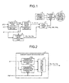
- FIG. 1 is a diagram of a configuration example of a power conversion control device according to the present invention.
- FIG. 1 shows, as an example, a power conversion control device of a form for controlling a power conversion unit 2 that supplies three-phase alternating-current power to an alternating-current electric motor 1.
- the power conversion unit 2 includes a plurality of switching elements.
- the power conversion unit 2 is a power conversion device that controls the switching elements according to an instruction (a switching signal) received from the power conversion control device having a below-mentioned configuration to thereby convert direct-current power supplied from a direct-current power source 3 into three-phase alternating-current power.
- the power conversion control device in the present embodiment includes a modulation-factor calculating unit 4, a carrier-wave generating unit 5, a modulation-wave generating unit 6, and a comparing unit 7.
- the modulation-factor calculating unit 4 calculates a modulation factor (PMF) based on an intermediate direct-current voltage (EFC) and an output voltage command (
- EFC is a voltage of direct-current power supplied from the direct-current power source 3 to the power conversion unit 2.
- the carrier-wave generating unit 5 generates carrier waves (Ca u , Ca v , and Ca w ) of a U phase, a V phase, and a W phase based on an output voltage phase angle command ( ⁇ *) and the modulation factor (PMF) calculated by the modulation-factor calculating unit 4. Details of the internal configuration of the carrier-wave generating unit 5 and a carrier wave generating operation are explained below.
- the modulation-wave generating unit 6 generates modulation waves ( ⁇ u , ⁇ v , and ⁇ w ) of the U phase, the V phase, and the W phase based on the output voltage phase angle command ( ⁇ *) and the modulation factor (PMF) calculated by the modulation-factor calculating unit 4.
- ⁇ * corresponds to the u phase
- w PMF ⁇ sin ⁇ - 4 ⁇ ⁇ / 3
- the comparing unit 7 operating as a switching-signal generating unit compares, for each of in-phases, the modulation waves ( ⁇ u , ⁇ v , and ⁇ w ) generated by the modulation-wave generating unit 6 and the carrier waves (Ca u , Ca v , and Ca w ) generated by the carrier-wave generating unit 5 and generates switching signals (SW u , SW v , and SW w ), which are control signals for the power conversion unit 2, based on the comparison result.
- the power conversion control device in the present embodiment controls the power conversion unit 2 in a synchronous PWM mode in which a carrier wave and a modulation wave used for the generation of the switching signal are synchronized with each other.
- FIG. 2 is a diagram of a configuration example of the carrier-wave generating unit 5.
- the carrier-wave generating unit 5 includes candidate-carrier-wave generating units 50a and 50b and a carrier-wave selecting unit 51.
- the candidate-carrier-wave generating unit 50a generates a first candidate carrier wave based on the output voltage phase angle command ( ⁇ *).
- the candidate-carrier-wave generating unit 50b generates a second candidate carrier wave based on the output voltage phase angle command ( ⁇ *) and the modulation factor (PMF) calculated by the modulation-factor calculating unit 4.
- ⁇ * the output voltage phase angle command
- PMF modulation factor
- the candidate-carrier-wave generating units 50a and 50b respectively generate candidate carrier waves of the U phase, the V phase, and the W phase.
- the carrier-wave selecting unit 51 selects, based on the modulation factor (PMF), the carrier waves (first candidate carrier waves of the U, V, and W phases) generated by the candidate-carrier-wave generating unit 50a or the carrier waves (second candidate carrier waves of the U, V, and W phases) generated by the candidate-carrier-wave generating unit 50b and outputs the carrier waves to the comparing unit 7 as the carrier waves Ca u , Ca v , and Ca w of the respective phases.
- PMF modulation factor
- the carrier-wave selecting unit 51 selects the carrier waves selected by the candidate-carrier-wave generating unit 50b. In the case of a non-overmodulation state, the carrier-wave selecting unit 51 selects the carrier waves generated by the candidate-carrier-wave generating unit 50a.
- the carrier waves (the first candidate carrier waves) generated by the candidate-carrier-wave generating unit 50a and the carrier waves (the second candidate carrier waves) generated by the candidate-carrier-wave generating unit 50b are explained.
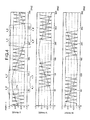
- FIG. 3 is a diagram of an example of the carrier waves generated by the candidate-carrier-wave generating unit 50a.
- a phase angle of a U-phase modulation wave is shown on the abscissa.
- the candidate-carrier-wave generating unit 50a generates carrier waves same as carrier waves in the past (e.g., carrier waves shown in FIGS. 6 and 7 of Patent Literature 1).
- the candidate-carrier-wave generating unit 50a can generate saw-tooth waves rather than the triangular waves.
- FIG. 4 and FIG. 5 are diagrams of examples of the carrier waves generated by the candidate-carrier-wave generating unit 50b.
- the candidate-carrier-wave generating unit 50b generates, as the carrier waves of the U, V, and W phases, signals that have a value fixed to -1 (or fixed to +1) in fixed sections (two a_b sections) centering on a peak position of modulation waves corresponding to the carrier waves (or positions shifted by a half cycle from the peak position) and are triangular waves same as the carrier waves in the past in other sections.
- the carrier wave of the U phase is fixed to -1 in a section of 90 ⁇ a_b [deg] and fixed to +1 in a section of 270 ⁇ a_b [deg].
- the carrier waves may be saw-tooth waves instead of the triangular waves.
- the a_b sections are shown only for the carrier wave in the U phase. However, in the V phase and the W phase, values are fixed to +1 or -1 in the same sections. The sections where the values are fixed fluctuate according to the modulation factor PMF.
- the carrier waves of the respective phases are set such that the triangular waves and the fixed waves (the signals fixed to +1 or -1) continuously connected.
- the carrier waves generated by the candidate-carrier-wave generating unit 50b can be considered as signals that are fixed to +1 or -1 in sections where the magnitudes (absolute values) of the modulation waves are larger than a predetermined threshold (a value smaller than the amplitude of the triangular waves; equivalent to ⁇ th shown in FIG. 4 ) and are triangular waves in other sections.
- a predetermined threshold a value smaller than the amplitude of the triangular waves; equivalent to ⁇ th shown in FIG. 4
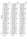
- FIG. 6 showing the switching patterns by the power conversion control device in the present embodiment and FIG. 8 showing the switching patterns in the past are compared, it is seen that the number of times of switching is smaller when the control by the power conversion control device in the present embodiment is applied than in the past. For example, concerning the U phase, in FIG. 6 , switching near 60 degrees (deg), near 120 degrees, near 240 degrees, and near 300 degrees, which occurs in FIG. 8 , is avoided.
- the power conversion control device in the present embodiment is configured such that the candidate-carrier-wave generating unit 50b generates the carrier waves explained above and, during the overmodulation, the comparing unit 7 generates the switching signals using the carrier waves. Therefore, in a power conversion control operation during the overmodulation, a narrow pulse is not included in the switching signals. It is possible to suppress the number of times of switching. The influence of the narrow pulse on the modulation accuracy is small. Therefore, by avoiding generation of the narrow pulse, it is possible to reduce a switching loss while preventing the modulation accuracy from being degraded.
- the modulation accuracy is information indicating an error between a voltage (an indicated voltage) indicated by an output voltage command and an actually output voltage.
- the carrier waves generated by the candidate-carrier-wave generating unit 50b are explained more in detail.
- the carrier wave of the U phase is explained with reference to FIG. 4 .
- the carrier waves of the V phase and the W phase are different from the carrier wave of the U phase only in a phase and are the same as the carrier wave of the U phase in a waveform. Therefore, explanation of the carrier waves of the V phase and the W phase is omitted.
- the carrier wave generated by the candidate-carrier-wave generating unit 50b is fixed to +1 or -1 so that a switching operation does not occur in a section represented by Formula (3a) and Formula (3b) below.
- Formula (3a) and Formula (3b) ⁇ / 2 - a_b ⁇ ⁇ ⁇ ⁇ / 2 + a_b 3 ⁇ ⁇ / 2 - a_b ⁇ ⁇ ⁇ 3 ⁇ ⁇ / 2 + a_b
- the carrier wave is fixed to +1 in the section of Formula (3a) and fixed to -1 in the section of Formula (3b).
- section width a_b used in Formulas (3a) and (3b) is determined as explained below with attention directed to ⁇ /2.
- An angle width equivalent to a carrier wave half cycle is represented as X.
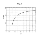
- a threshold ⁇ th is given as a condition for the magnitude of the U-phase modulation wave at this timing and is defined as Formula (5).
- ⁇ th relates to an allowable minimum pulse width and is set, for example, between 0.5 and 1.0.
- PMFsin ⁇ ⁇ / 2 - a_b ⁇ ⁇ th
- FIG. 9 indicates that, as the modulation factor PMF is larger, a section where a modulation wave exceeds 1 increases and the width (a_b ⁇ 2) of a section where switching is stopped (a carrier wave is fixed to +1 or -1) and a_b' obtained by adding a half cycle of the carrier wave to a_b expand.
- the candidate-carrier-wave generating unit 50b sets, according to the characteristic curve shown in FIG. 9 , the switching stop sections (a_b and a_b') corresponding to the modulation factor PMF and generates carrier waves having the waveforms shown in FIG. 4 and FIG. 5 .
- the candidate-carrier-wave generating unit 50b may generate, when the modulation factor PMF is equal to or smaller than 1, carrier waves same as the carrier waves in the past and generate, when the modulation factor PMF exceeds 1, carrier waves having a fixed value (+1 or -1) in a section corresponding to a value of PMF and output the carrier waves to the comparing unit 7.
- the power conversion control device in the present embodiment uses the synchronous PWM control for controlling the power conversion device in the synchronous PWM mode.
- the power conversion control device includes the carrier-wave generating unit that outputs, in the case of the overmodulation state, a fixed value (-1 or +1) in first sections (the non-crossing sections explained above and near the non-crossing sections) centering on a peak position of a modulation signal and a position shifted by a half cycle from the peak position and having a length corresponding to a modulation factor and that outputs triangular waves in the remaining second sections.
- the power conversion control device generates, using the carrier waves generated by the carrier-wave generating unit, PWM control signals (switching signals) for controlling a power conversion circuit.
- the first sections are determined using the modulation factor and the magnitude of the modulation waves (equivalent to ⁇ th explained above). Therefore, it is possible to quantitatively set a suppressing effect for the numbers of times of switching.
- the first sections are set such that the carrier waves in the sections and the carrier waves in the second sections are continuously connected, that is, the continuity of the carrier waves is maintained in boundary portions between the first sections and the second sections. Therefore, it is possible to surely avoid occurrence of unnecessary switching.
- a voltage input to an electric motor can be set higher by applying the power conversion control device in the present embodiment. Therefore, an input current can be suppressed and thus a Joule loss (mainly, a copper loss) due to an electric current decreases. That is, a loss of the electric motor decreases and thus the cooling performance can be suppressed. Therefore, it is possible to reduce the size and the weight of the electric motor by reviewing a cooling fin shape and a cooling air passage.
- a Joule loss mainly, a copper loss
- the carrier waves in sections of the second sections other than the boundary portions between the second sections and the first sections are also generated in synchronization with the modulation waves. This is more preferable because it is possible to easily realize the configuration of the carrier-wave generating unit.
- the power conversion device that converts direct-current power into three-phase alternating-current power is controlled.
- the power conversion control device can also be applied to control of a power conversion device that converts the direct-current power into single-phase alternating-current power and a switching loss can be reduced.
- FIG. 10 is a diagram of a configuration example in which the power conversion control device is applied to a railway vehicle as a vehicle driving system.
- the vehicle driving system includes the alternating-current electric motor 1, the power conversion unit 2, a control unit 8, and an input circuit 12.
- the alternating-current electric motor 1 is the same as the alternating-current electric motor 1 shown in FIG. 1 and is mounted on the railway vehicle.
- the power conversion unit 2 is the same as the power conversion unit 2 shown in FIG. 1 .
- the power conversion unit 2 converts the direct-current power supplied from the input circuit 12 into alternating-current power and drives the alternating-current electric motor 1.
- the control unit 8 is equivalent to the power conversion control device explained in the first embodiment.
- control unit 8 is configured to include the modulation-factor calculating unit 4, the carrier-wave generating unit 5, the modulation-wave generating unit 6, and the comparing unit 7 explained in the first embodiment.
- the control unit 8 generates the switching signals (SWu, SWv, and SWw) for controlling the power conversion unit 2.
- the input circuit 12 is configured to include a switch, a filter capacitor, a filter reactor, and the like. One end of the input circuit 12 is connected to an overhead line 10 via a current collector 11. The other end of the input circuit 12 is connected to a rail 14, which is ground potential, via a wheel 13. The input circuit 12 receives supply of the direct-current power or alternating-current power from the overhead line 10 and generates direct-current power supplied to the power conversion unit 2.
- the present invention is useful as the power conversion control device that performs control capable of reducing a switching loss during power conversion.
Abstract
Description
- The present invention relates to a power conversion control device for controlling a power conversion device that drives a three-phase alternating-current electric motor and the like.
- There is
Patent Literature 1 as a literature in which power conversion control in the past is described.Patent Literature 1 explains a technology for solving various problems that occur when a control mode of an inverter is switched, specifically, a problem in which a switching frequency becomes discontinuous and a tone change of magnetic noise caused due to the discontinuous switching frequency is harsh on the ears and a problem in which fluctuation occurs in generated torque of an electric motor. According to the technology described inPatent Literature 1, it is also possible to solve a problem in which the number of generated pulses becomes unstable in a section where crossing of a carrier wave and a modulation wave frequently occurs (near a zero-cross of the modulation wave) in an operation in an overmodulation state, in which the modulation factor exceeds 100%, and an asynchronous PWM mode (a state in which the modulation wave and the carrier wave are not synchronous with each other). - Patent Literature 1: Japanese Patent No.
3455788 - In the case of the overmodulation state, there is a section where the crossing of the modulation wave and the carrier wave does not occur and extremely narrow pulses are generated near the section. The influence of the extremely narrow pulses on an output voltage of an inverter is small. Even if the pulses are absent, the output voltage hardly changes. On the other hand, the number of times of switching of a switching element configuring the inverter depends on only the number of pulses. Therefore, when pulses hardly affecting the inverter output (the extremely narrow pulses) are present, there is a problem in that a switching loss unnecessarily increases.
- The present invention has been devised in view of the above and it is an object of the present invention to obtain a power conversion control device, a power conversion control method, an electric motor, and a vehicle driving system capable of reducing a switching loss related to a power converting operation.
- In order to solve the above problems and achieve the object, the present invention is a power conversion control device that controls, based on a modulation wave and a carrier wave, a power conversion device that converts direct-current power into alternating-current power, including a modulation-wave generating unit that generates a modulation wave based on an output voltage phase angle command, a direct-current voltage supplied to the power conversion device, and a modulation factor calculated based on an output voltage command; a carrier-wave generating unit that, in a case of a non-overmodulation state, generates a triangular wave or a saw-tooth wave as the carrier wave, and, in a case of an overmodulation state, generates, as the carrier wave, a signal fixed to -1 in a first section that is a predetermined range centering on a timing corresponding to a peak position of the modulation wave, generates, as the carrier wave, a signal fixed to +1 in a second section obtained by shifting the first section by a half cycle of the modulation wave, and generates, as the carrier wave, a triangular wave or a saw-tooth wave in a remaining third section; and a switching-signal generating unit that compares the carrier wave and the modulation wave and generates a switching signal for controlling the power conversion device.
- According to the present invention, it is possible to prevent a narrow pulse from being included in a switching signal and suppress the number of times of switching in a power conversion device. That is, there is an effect that it is possible to realize a power conversion control device capable of performing control for reducing a switching loss while preventing a modulation accuracy from being deteriorated.
-
-
FIG. 1 is a diagram of a configuration example of a power conversion control device according to the present invention. -
FIG. 2 is a diagram of a configuration example of a carrier-wave generating unit. -
FIG. 3 is a diagram of an example of carrier waves generated by a candidate-carrier-wave generating unit. -
FIG. 4 is a diagram of an example of carrier waves generated by a candidate-carrier-wave generating unit. -
FIG. 5 is a diagram of an example of the carrier waves generated by the candidate-carrier-wave generating unit. -
FIG. 6 is a diagram of an example of switching signals generated using the carrier waves shown inFIG. 4 . -
FIG. 7 is a diagram of an example of carrier waves generated by a power conversion control device in the past. -
FIG. 8 is a diagram of an example of switching signals generated using the carrier waves in the past. -
FIG. 9 is a diagram of an example of a relation between a modulation factor and a switching stop section. -
FIG. 10 is a diagram of a configuration example of a vehicle driving system. - Embodiments of a power conversion control device, a power conversion control method, an electric motor, and a vehicle driving system according to the present invention are explained in detail below based on the drawings. Note that the present invention is not limited by the embodiments.
-
FIG. 1 is a diagram of a configuration example of a power conversion control device according to the present invention.FIG. 1 shows, as an example, a power conversion control device of a form for controlling apower conversion unit 2 that supplies three-phase alternating-current power to an alternating-currentelectric motor 1. Note that thepower conversion unit 2 includes a plurality of switching elements. Thepower conversion unit 2 is a power conversion device that controls the switching elements according to an instruction (a switching signal) received from the power conversion control device having a below-mentioned configuration to thereby convert direct-current power supplied from a direct-current power source 3 into three-phase alternating-current power. - As shown in
FIG. 1 , the power conversion control device in the present embodiment includes a modulation-factor calculating unit 4, a carrier-wave generating unit 5, a modulation-wave generating unit 6, and acomparing unit 7. - The modulation-
factor calculating unit 4 calculates a modulation factor (PMF) based on an intermediate direct-current voltage (EFC) and an output voltage command (|V*|). The EFC is a voltage of direct-current power supplied from the direct-current power source 3 to thepower conversion unit 2. The modulation-factor calculating unit 4 calculates the PMF according to the following formula:
- The carrier-
wave generating unit 5 generates carrier waves (Cau, Cav, and Caw) of a U phase, a V phase, and a W phase based on an output voltage phase angle command (θ*) and the modulation factor (PMF) calculated by the modulation-factor calculating unit 4. Details of the internal configuration of the carrier-wave generating unit 5 and a carrier wave generating operation are explained below. - The modulation-wave generating unit 6 generates modulation waves (αu, αv, and αw) of the U phase, the V phase, and the W phase based on the output voltage phase angle command (θ*) and the modulation factor (PMF) calculated by the modulation-
factor calculating unit 4. When θ* corresponds to the u phase, the modulation-wave generating unit 6 generates modulation waves of the respective phases according to the following formula:
- The comparing
unit 7 operating as a switching-signal generating unit compares, for each of in-phases, the modulation waves (αu, αv, and αw) generated by the modulation-wave generating unit 6 and the carrier waves (Cau, Cav, and Caw) generated by the carrier-wave generatingunit 5 and generates switching signals (SWu, SWv, and SWw), which are control signals for thepower conversion unit 2, based on the comparison result. The power conversion control device in the present embodiment controls thepower conversion unit 2 in a synchronous PWM mode in which a carrier wave and a modulation wave used for the generation of the switching signal are synchronized with each other. - Details of the carrier-
wave generating unit 5 are explained.FIG. 2 is a diagram of a configuration example of the carrier-wave generating unit 5. As shown in the figure, the carrier-wave generating unit 5 includes candidate-carrier-wave generating units wave selecting unit 51. The candidate-carrier-wave generating unit 50a generates a first candidate carrier wave based on the output voltage phase angle command (θ*). The candidate-carrier-wave generating unit 50b generates a second candidate carrier wave based on the output voltage phase angle command (θ*) and the modulation factor (PMF) calculated by the modulation-factor calculating unit 4. Note that the candidate-carrier-wave generating units wave selecting unit 51 selects, based on the modulation factor (PMF), the carrier waves (first candidate carrier waves of the U, V, and W phases) generated by the candidate-carrier-wave generatingunit 50a or the carrier waves (second candidate carrier waves of the U, V, and W phases) generated by the candidate-carrier-wave generatingunit 50b and outputs the carrier waves to the comparingunit 7 as the carrier waves Cau, Cav, and Caw of the respective phases. In the case of an overmodulation state (in the case of PMF>1), the carrier-wave selecting unit 51 selects the carrier waves selected by the candidate-carrier-wave generating unit 50b. In the case of a non-overmodulation state, the carrier-wave selecting unit 51 selects the carrier waves generated by the candidate-carrier-wave generating unit 50a. - The carrier waves (the first candidate carrier waves) generated by the candidate-carrier-wave generating
unit 50a and the carrier waves (the second candidate carrier waves) generated by the candidate-carrier-wave generating unit 50b are explained. -
FIG. 3 is a diagram of an example of the carrier waves generated by the candidate-carrier-wave generatingunit 50a. The candidate-carrier-wave generatingunit 50a generates, as the carrier waves, triangular waves shown in the figure. Note that, for convenience of explanation, modulation waves in the case of PMF=0.5 are also described. The modulation waves are indicated by chain lines. InFIG. 3 , a phase angle of a U-phase modulation wave is shown on the abscissa. As shown in the figure, the candidate-carrier-wave generatingunit 50a generates carrier waves same as carrier waves in the past (e.g., carrier waves shown inFIGS. 6 and7 of Patent Literature 1). The candidate-carrier-wave generating unit 50a can generate saw-tooth waves rather than the triangular waves. -
FIG. 4 andFIG. 5 are diagrams of examples of the carrier waves generated by the candidate-carrier-wave generating unit 50b.FIG. 4 shows an example of carrier waves generated in the case of PMF=1.1.FIG. 5 shows an example of carrier waves generated in the case of PMF=1.5. As shown inFIG. 4 andFIG. 5 , the candidate-carrier-wave generating unit 50b generates, as the carrier waves of the U, V, and W phases, signals that have a value fixed to -1 (or fixed to +1) in fixed sections (two a_b sections) centering on a peak position of modulation waves corresponding to the carrier waves (or positions shifted by a half cycle from the peak position) and are triangular waves same as the carrier waves in the past in other sections. For example, the carrier wave of the U phase is fixed to -1 in a section of 90±a_b [deg] and fixed to +1 in a section of 270±a_b [deg]. The carrier waves may be saw-tooth waves instead of the triangular waves. The a_b sections are shown only for the carrier wave in the U phase. However, in the V phase and the W phase, values are fixed to +1 or -1 in the same sections. The sections where the values are fixed fluctuate according to the modulation factor PMF. The carrier waves of the respective phases are set such that the triangular waves and the fixed waves (the signals fixed to +1 or -1) continuously connected. To put it differently, the carrier waves generated by the candidate-carrier-wave generating unit 50b can be considered as signals that are fixed to +1 or -1 in sections where the magnitudes (absolute values) of the modulation waves are larger than a predetermined threshold (a value smaller than the amplitude of the triangular waves; equivalent to αth shown inFIG. 4 ) and are triangular waves in other sections. -
FIG. 6 is a diagram of an example of switching signals (switching patterns) generated by the comparingunit 7 in the case of PMF=1.1, that is, when the carrier waves shown inFIG. 4 are used.FIG. 7 is a diagram of an example of carrier waves generated by a power conversion control device in the past. Modulation waves in the case of PMF=1.1 are also described. As shown in the figure, in the overmodulation state, the power conversion control device in the past generates carrier waves same as carrier waves generated in a non-overmodulation state (a state of PMF≤1.0). When the carrier waves in the past shown inFIG. 7 are used, if PMF=1.1, switching patterns shown inFIG. 8 are obtained. - When
FIG. 6 showing the switching patterns by the power conversion control device in the present embodiment andFIG. 8 showing the switching patterns in the past are compared, it is seen that the number of times of switching is smaller when the control by the power conversion control device in the present embodiment is applied than in the past. For example, concerning the U phase, inFIG. 6 , switching near 60 degrees (deg), near 120 degrees, near 240 degrees, and near 300 degrees, which occurs inFIG. 8 , is avoided. - As explained above, the power conversion control device in the present embodiment is configured such that the candidate-carrier-
wave generating unit 50b generates the carrier waves explained above and, during the overmodulation, the comparingunit 7 generates the switching signals using the carrier waves. Therefore, in a power conversion control operation during the overmodulation, a narrow pulse is not included in the switching signals. It is possible to suppress the number of times of switching. The influence of the narrow pulse on the modulation accuracy is small. Therefore, by avoiding generation of the narrow pulse, it is possible to reduce a switching loss while preventing the modulation accuracy from being degraded. Note that the modulation accuracy is information indicating an error between a voltage (an indicated voltage) indicated by an output voltage command and an actually output voltage. Because synchronous PWM control (control in a synchronous PWM mode) is performed, it is possible to prevent the numbers of times of switching of three phases from becoming unbalanced near a boundary between a non-crossing section where a carrier wave and a modulation wave do not cross each other during the overmodulation and a crossing occurrence section where the crossing occurs. It is possible to prevent pulsation of a load current (a beat phenomenon) from occurring. That is, it is possible to stabilize the number of generated pulses and prevent occurrence of imbalance of the numbers of times of switching without performing difficult control for solving the problem in that the number of generated pulses becomes unstable, which needs to be performed in the power conversion control in the past that performs a control in the asynchronous PWM mode during the overmodulation. - The carrier waves generated by the candidate-carrier-
wave generating unit 50b are explained more in detail. The carrier wave of the U phase is explained with reference toFIG. 4 . The carrier waves of the V phase and the W phase are different from the carrier wave of the U phase only in a phase and are the same as the carrier wave of the U phase in a waveform. Therefore, explanation of the carrier waves of the V phase and the W phase is omitted. - Compared with the carrier wave that is generated by the candidate-carrier-
wave generating unit 50a and is the same as the carrier waves in the past, the carrier wave generated by the candidate-carrier-wave generating unit 50b is fixed to +1 or -1 so that a switching operation does not occur in a section represented by Formula (3a) and Formula (3b) below.

- The carrier wave is fixed to +1 in the section of Formula (3a) and fixed to -1 in the section of Formula (3b). Note that the section width a_b used in Formulas (3a) and (3b) is determined as explained below with attention directed to θ≤π/2. An angle width equivalent to a carrier wave half cycle is represented as X. X satisfies the following Formula (4):

- To determine a switching timing condition θ=π/2-a_b' closest to π/2 in the section of 0<θ<π/2, a threshold αth is given as a condition for the magnitude of the U-phase modulation wave at this timing and is defined as Formula (5). In the formula, αth relates to an allowable minimum pulse width and is set, for example, between 0.5 and 1.0.

- Formula (5) can be transformed into the following Formula (6):

- When αth=0.95 is set in Formula (6), the characteristic of a_b' with respect to the modulation factor PMF is as shown in
FIG. 9. FIG. 9 indicates that, as the modulation factor PMF is larger, a section where a modulation wave exceeds 1 increases and the width (a_b×2) of a section where switching is stopped (a carrier wave is fixed to +1 or -1) and a_b' obtained by adding a half cycle of the carrier wave to a_b expand. - As explained above, the candidate-carrier-
wave generating unit 50b sets, according to the characteristic curve shown inFIG. 9 , the switching stop sections (a_b and a_b') corresponding to the modulation factor PMF and generates carrier waves having the waveforms shown inFIG. 4 andFIG. 5 . - Note that the configuration of the carrier-
wave generating unit 5 is not limited to the configuration shown inFIG. 2 . The candidate-carrier-wave generating unit 50b may generate, when the modulation factor PMF is equal to or smaller than 1, carrier waves same as the carrier waves in the past and generate, when the modulation factor PMF exceeds 1, carrier waves having a fixed value (+1 or -1) in a section corresponding to a value of PMF and output the carrier waves to the comparingunit 7. - As explained above, the power conversion control device in the present embodiment uses the synchronous PWM control for controlling the power conversion device in the synchronous PWM mode. The power conversion control device includes the carrier-wave generating unit that outputs, in the case of the overmodulation state, a fixed value (-1 or +1) in first sections (the non-crossing sections explained above and near the non-crossing sections) centering on a peak position of a modulation signal and a position shifted by a half cycle from the peak position and having a length corresponding to a modulation factor and that outputs triangular waves in the remaining second sections. The power conversion control device generates, using the carrier waves generated by the carrier-wave generating unit, PWM control signals (switching signals) for controlling a power conversion circuit. Accordingly, it is possible to prevent a narrow pulse from being included in the PWM control signals; therefore, it is possible to suppress the number of times of switching and reduce a switching loss. In addition, it is possible to prevent the numbers of times of switching of the three phases from becoming unbalanced. It is possible to prevent unnecessary pulsation from occurring in a load current.
- The first sections are determined using the modulation factor and the magnitude of the modulation waves (equivalent to αth explained above). Therefore, it is possible to quantitatively set a suppressing effect for the numbers of times of switching.
- The first sections are set such that the carrier waves in the sections and the carrier waves in the second sections are continuously connected, that is, the continuity of the carrier waves is maintained in boundary portions between the first sections and the second sections. Therefore, it is possible to surely avoid occurrence of unnecessary switching.
- Further, a voltage input to an electric motor can be set higher by applying the power conversion control device in the present embodiment. Therefore, an input current can be suppressed and thus a Joule loss (mainly, a copper loss) due to an electric current decreases. That is, a loss of the electric motor decreases and thus the cooling performance can be suppressed. Therefore, it is possible to reduce the size and the weight of the electric motor by reviewing a cooling fin shape and a cooling air passage.
- Note that, in order to maintain the continuity of the carrier waves, the carrier waves in sections of the second sections other than the boundary portions between the second sections and the first sections are also generated in synchronization with the modulation waves. This is more preferable because it is possible to easily realize the configuration of the carrier-wave generating unit.
- Note that, in the above explanation, the power conversion device that converts direct-current power into three-phase alternating-current power is controlled. However, the power conversion control device can also be applied to control of a power conversion device that converts the direct-current power into single-phase alternating-current power and a switching loss can be reduced.
- In the present embodiment, a vehicle driving system applied with the power conversion control device explained in the first embodiment is explained.
-
FIG. 10 is a diagram of a configuration example in which the power conversion control device is applied to a railway vehicle as a vehicle driving system. The vehicle driving system includes the alternating-currentelectric motor 1, thepower conversion unit 2, acontrol unit 8, and aninput circuit 12. The alternating-currentelectric motor 1 is the same as the alternating-currentelectric motor 1 shown inFIG. 1 and is mounted on the railway vehicle. Thepower conversion unit 2 is the same as thepower conversion unit 2 shown inFIG. 1 . Thepower conversion unit 2 converts the direct-current power supplied from theinput circuit 12 into alternating-current power and drives the alternating-currentelectric motor 1. Thecontrol unit 8 is equivalent to the power conversion control device explained in the first embodiment. That is, thecontrol unit 8 is configured to include the modulation-factor calculating unit 4, the carrier-wave generating unit 5, the modulation-wave generating unit 6, and the comparingunit 7 explained in the first embodiment. Thecontrol unit 8 generates the switching signals (SWu, SWv, and SWw) for controlling thepower conversion unit 2. - Although not shown in the figure, the
input circuit 12 is configured to include a switch, a filter capacitor, a filter reactor, and the like. One end of theinput circuit 12 is connected to anoverhead line 10 via acurrent collector 11. The other end of theinput circuit 12 is connected to arail 14, which is ground potential, via awheel 13. Theinput circuit 12 receives supply of the direct-current power or alternating-current power from theoverhead line 10 and generates direct-current power supplied to thepower conversion unit 2. - By applying the power conversion control device in the present embodiment to the vehicle driving system in this way, it is possible to realize a reduction in a loss and a reduction in the size of the entire system.
- As explained above, the present invention is useful as the power conversion control device that performs control capable of reducing a switching loss during power conversion.
-
- 1
- alternating-current electric motor
- 2
- power conversion unit
- 3
- direct-current power source
- 4
- modulation-factor calculating unit
- 5
- carrier-wave generating unit
- 6
- modulation-wave generating unit
- 7
- comparing unit
- 50a, 50b
- candidate-carrier-wave generating unit
- 51
- carrier-wave selecting unit
- 8
- control unit
- 10
- overhead line
- 11
- current collector
- 12
- input circuit
- 13
- wheel
- 14
- rail
Claims (8)
- A power conversion control device that controls, based on a modulation wave and a carrier wave, a power conversion device that converts direct-current power into alternating-current power, the device comprising:a modulation-wave generating unit that generates a modulation wave based on an output voltage phase angle command, a direct-current voltage supplied to the power conversion device, and a modulation factor calculated based on an output voltage command;a carrier-wave generating unit that, in a case of a non-overmodulation state, generates a triangular wave or a saw-tooth wave as the carrier wave, and, in a case of an overmodulation state, generates, as the carrier wave, a signal fixed to -1 in a first section that is a predetermined range centering on a timing corresponding to a peak position of the modulation wave, generates, as the carrier wave, a signal fixed to +1 in a second section obtained by shifting the first section by a half cycle of the modulation wave, and generates, as the carrier wave, a triangular wave or a saw-tooth wave in a remaining third section; anda switching-signal generating unit that compares the carrier wave and the modulation wave and generates a switching signal for controlling the power conversion device.
- The power conversion control device according to claim 1, wherein the carrier-wave generating unit generates a carrier wave synchronizing with a modulation wave.
- The power conversion control device according to claims 1 and 2, wherein
the carrier-wave generating unit includesa first candidate-carrier-wave generating unit that generates, based on an output voltage phase angle command, a carrier wave used in a case of a non-overmodulation state as a first candidate carrier wave,a second candidate-carrier-wave generating unit that generates, based on an output voltage phase angle command and a modulation factor, a carrier wave used in a case of an overmodulation state as a second candidate carrier wave, anda carrier-wave selecting unit that selects the first candidate carrier wave and outputs the first candidate carrier wave as the carrier wave in a case of a non-overmodulation state and selects the second candidate carrier wave and outputs the second candidate carrier wave as the carrier wave in a case of an overmodulation state. - The power conversion control device according to claim 1 or 2, wherein the carrier-wave generating unit sets the first section based on a modulation factor.
- The power conversion control device according to claim 1 or 2, wherein the carrier-wave generating unit generates a carrier wave in which a continuity is maintained in a boundary between the first section or the second section and the third section.
- A power conversion control method in controlling, based on a modulation wave and a carrier wave, a power conversion device that converts direct-current power into alternating-current power, the method comprising:a modulation-wave generating step of generating a modulation wave based on an output voltage phase angle command, a direct-current voltage supplied to the power conversion device, and a modulation factor calculated based on an output voltage command;a carrier-wave generating step of, in a case of a non-overmodulation state, generating a triangular wave or a saw-tooth wave as the carrier wave, and, in a case of an overmodulation state, generating, as the carrier wave, a signal fixed to -1 in a first section that is a predetermined range centering on a timing corresponding to a peak position of the modulation wave, generating, as the carrier wave, a signal fixed to +1 in a second section obtained by shifting the first section by a half cycle of the modulation wave, and generating, as the carrier wave, a triangular wave or a saw-tooth wave in a remaining third section; anda switching-signal generating step of comparing the carrier wave and the modulation wave and generating a switching signal for controlling the power conversion device.
- An electric motor driven by a power conversion device controlled by the power conversion control device according to any one of claims 1 to 5.
- A vehicle driving system comprising:the power conversion control device according to any one of claims 1 to 5;a power conversion device controlled by the power conversion control device;an input circuit that generates direct-current power input to the power conversion device; andan electric motor driven by the power conversion device.
Applications Claiming Priority (1)
| Application Number | Priority Date | Filing Date | Title |
|---|---|---|---|
| PCT/JP2011/072645 WO2013046462A1 (en) | 2011-09-30 | 2011-09-30 | Power conversion control device, power conversion control method, electric motor and vehicle drive system |
Publications (3)
| Publication Number | Publication Date |
|---|---|
| EP2763313A1 true EP2763313A1 (en) | 2014-08-06 |
| EP2763313A4 EP2763313A4 (en) | 2015-12-02 |
| EP2763313B1 EP2763313B1 (en) | 2017-02-01 |
Family
ID=47994564
Family Applications (1)
| Application Number | Title | Priority Date | Filing Date |
|---|---|---|---|
| EP11873497.9A Active EP2763313B1 (en) | 2011-09-30 | 2011-09-30 | Power conversion control device, power conversion control method, electric motor and vehicle drive system |
Country Status (11)
| Country | Link |
|---|---|
| US (1) | US9385630B2 (en) |
| EP (1) | EP2763313B1 (en) |
| JP (1) | JP5551833B2 (en) |
| KR (1) | KR101636629B1 (en) |
| CN (1) | CN103828226B (en) |
| BR (1) | BR112014006857A2 (en) |
| CA (1) | CA2850452C (en) |
| ES (1) | ES2617782T3 (en) |
| IN (1) | IN2014CN02927A (en) |
| MX (1) | MX2014003616A (en) |
| WO (1) | WO2013046462A1 (en) |
Families Citing this family (12)
| Publication number | Priority date | Publication date | Assignee | Title |
|---|---|---|---|---|
| BR112014007621A2 (en) * | 2011-09-30 | 2017-04-18 | Mitsubishi Electric Corp | control device and method for an electric motor, electric motor, and vehicle drive system |
| CN105075097B (en) * | 2013-04-23 | 2019-06-18 | 三菱电机株式会社 | Power-converting device |
| DE112013006976T5 (en) | 2013-04-23 | 2015-12-31 | Mitsubishi Electric Corporation | Control unit of an electric AC motor |
| JP5962591B2 (en) * | 2013-06-03 | 2016-08-03 | 株式会社デンソー | Motor drive device |
| JP6145025B2 (en) * | 2013-10-29 | 2017-06-07 | 東洋電機製造株式会社 | Inverter control device |
| JP5986595B2 (en) * | 2014-02-20 | 2016-09-06 | 株式会社豊田中央研究所 | Power converter control device and motor system including the same |
| WO2016031030A1 (en) * | 2014-08-28 | 2016-03-03 | 三菱電機株式会社 | Electric power conversion device and vehicle drive system |
| JP5844006B1 (en) * | 2014-08-28 | 2016-01-13 | 三菱電機株式会社 | Power conversion device and vehicle drive system |
| JP6173409B2 (en) * | 2015-11-19 | 2017-08-02 | 三菱電機株式会社 | Power conversion device and vehicle drive system |
| EP3324527B1 (en) * | 2016-11-18 | 2021-06-30 | Aros Electronics AB | Dc bus ripple elimination for multiphase electric machines |
| JP7112593B2 (en) * | 2019-04-12 | 2022-08-03 | 株式会社日立産機システム | POWER CONVERTER AND CONTROL METHOD THEREOF |
| CN111682783A (en) * | 2020-06-01 | 2020-09-18 | 新风光电子科技股份有限公司 | High-voltage frequency conversion all-in-one machine adopting trapezoidal modulation waves and control method thereof |
Family Cites Families (13)
| Publication number | Priority date | Publication date | Assignee | Title |
|---|---|---|---|---|
| US4490606A (en) * | 1982-04-26 | 1984-12-25 | Geosource Inc. | Transducer apparatus utilizing fiber optics for data transmission |
| ZA949795B (en) * | 1993-12-17 | 1995-08-18 | Hitachi Ltd | Electric power conversion equipment. |
| JP3455788B2 (en) | 1993-12-17 | 2003-10-14 | 株式会社日立製作所 | Power converter |
| JPH09308256A (en) | 1996-05-14 | 1997-11-28 | Hitachi Ltd | Pwm inverter apparatus |
| CN1299426C (en) * | 2003-08-01 | 2007-02-07 | 清华大学 | Method for reducing three-level frequency converter swithcing loss |
| JP2005318755A (en) * | 2004-04-30 | 2005-11-10 | Kansai Electric Power Co Inc:The | Inverter control system |
| US7499290B1 (en) * | 2004-05-19 | 2009-03-03 | Mississippi State University | Power conversion |
| JP3811898B2 (en) | 2004-08-16 | 2006-08-23 | 株式会社日立製作所 | Electric vehicle power converter |
| JP2007110811A (en) * | 2005-10-12 | 2007-04-26 | Yaskawa Electric Corp | Inverter apparatus and control method for the same |
| JP4858597B2 (en) | 2008-11-28 | 2012-01-18 | 株式会社デンソー | Rotating machine control device and manufacturing method thereof |
| JP2010221856A (en) * | 2009-03-24 | 2010-10-07 | Hitachi Automotive Systems Ltd | Steering control device |
| JP2011135762A (en) | 2009-11-27 | 2011-07-07 | Toyota Central R&D Labs Inc | Ac motor drive-control apparatus and reference magnetic-flux calculation device |
| CN105075097B (en) | 2013-04-23 | 2019-06-18 | 三菱电机株式会社 | Power-converting device |
-
2011
- 2011-09-30 ES ES11873497.9T patent/ES2617782T3/en active Active
- 2011-09-30 WO PCT/JP2011/072645 patent/WO2013046462A1/en active Application Filing
- 2011-09-30 EP EP11873497.9A patent/EP2763313B1/en active Active
- 2011-09-30 IN IN2927CHN2014 patent/IN2014CN02927A/en unknown
- 2011-09-30 CA CA2850452A patent/CA2850452C/en not_active Expired - Fee Related
- 2011-09-30 US US14/347,658 patent/US9385630B2/en active Active
- 2011-09-30 MX MX2014003616A patent/MX2014003616A/en active IP Right Grant
- 2011-09-30 CN CN201180073686.1A patent/CN103828226B/en active Active
- 2011-09-30 KR KR1020147010870A patent/KR101636629B1/en active IP Right Grant
- 2011-09-30 JP JP2013535799A patent/JP5551833B2/en active Active
- 2011-09-30 BR BR112014006857A patent/BR112014006857A2/en not_active IP Right Cessation
Also Published As
| Publication number | Publication date |
|---|---|
| JP5551833B2 (en) | 2014-07-16 |
| CA2850452C (en) | 2017-06-20 |
| KR20140065469A (en) | 2014-05-29 |
| CA2850452A1 (en) | 2013-04-04 |
| EP2763313A4 (en) | 2015-12-02 |
| WO2013046462A1 (en) | 2013-04-04 |
| BR112014006857A2 (en) | 2017-04-04 |
| US20140232318A1 (en) | 2014-08-21 |
| CN103828226B (en) | 2016-04-20 |
| ES2617782T3 (en) | 2017-06-19 |
| IN2014CN02927A (en) | 2015-07-03 |
| CN103828226A (en) | 2014-05-28 |
| KR101636629B1 (en) | 2016-07-05 |
| MX2014003616A (en) | 2014-06-05 |
| JPWO2013046462A1 (en) | 2015-03-26 |
| EP2763313B1 (en) | 2017-02-01 |
| US9385630B2 (en) | 2016-07-05 |
Similar Documents
| Publication | Publication Date | Title |
|---|---|---|
| EP2763313B1 (en) | Power conversion control device, power conversion control method, electric motor and vehicle drive system | |
| CN101291115B (en) | Power inversion device and control method thereof | |
| EP2763312B1 (en) | Control device and control method for electric motor, and motor and vehicle drive system to which the control device and control method are applied | |
| JP5122505B2 (en) | Power conversion apparatus and control method thereof | |
| US8030874B2 (en) | Power converting apparatus | |
| JP5866065B2 (en) | AC motor control device | |
| US9647575B2 (en) | Power converter | |
| JP5916526B2 (en) | Power converter control device and multi-winding motor drive device | |
| JP5466830B2 (en) | Multi-phase motor drive | |
| EP2413488A1 (en) | Method of controlling power conversion device | |
| JP5449441B2 (en) | Synchronous machine controller | |
| JP5593362B2 (en) | Multi-phase motor drive | |
| JP6208089B2 (en) | Three-level three-phase inverter drive controller | |
| EP1887680A2 (en) | Control apparatus for semiconductor power converter | |
| WO2016031030A1 (en) | Electric power conversion device and vehicle drive system | |
| JP2007274829A (en) | System for controlling multiple inverter | |
| JP5085408B2 (en) | Multi-phase motor drive | |
| JP4539192B2 (en) | AC motor control device | |
| JP5717902B2 (en) | Power conversion control device, electric motor, and vehicle drive system | |
| EP4148969A1 (en) | Power conversion device and control method thereof | |
| WO2024042942A1 (en) | Drive control apparatus and drive control method for rotating electrical machine | |
| EP4213372A1 (en) | Open winding motor driving device | |
| EP3848227A1 (en) | Drive control device, drive control method, and rail vehicle mounted with said drive control device | |
| JP2012085405A (en) | Power converter, power conversion method and motor drive system |
Legal Events
| Date | Code | Title | Description |
|---|---|---|---|
| PUAI | Public reference made under article 153(3) epc to a published international application that has entered the european phase |
Free format text: ORIGINAL CODE: 0009012 |
|
| 17P | Request for examination filed |
Effective date: 20140423 |
|
| AK | Designated contracting states |
Kind code of ref document: A1 Designated state(s): AL AT BE BG CH CY CZ DE DK EE ES FI FR GB GR HR HU IE IS IT LI LT LU LV MC MK MT NL NO PL PT RO RS SE SI SK SM TR |
|
| DAX | Request for extension of the european patent (deleted) | ||
| REG | Reference to a national code |
Ref country code: DE Ref legal event code: R079 Ref document number: 602011034860 Country of ref document: DE Free format text: PREVIOUS MAIN CLASS: H02P0027060000 Ipc: H02P0027080000 |
|
| RA4 | Supplementary search report drawn up and despatched (corrected) |
Effective date: 20151029 |
|
| RIC1 | Information provided on ipc code assigned before grant |
Ipc: H02P 27/08 20060101AFI20151023BHEP Ipc: H02M 7/5387 20070101ALI20151023BHEP |
|
| GRAP | Despatch of communication of intention to grant a patent |
Free format text: ORIGINAL CODE: EPIDOSNIGR1 |
|
| INTG | Intention to grant announced |
Effective date: 20160928 |
|
| GRAS | Grant fee paid |
Free format text: ORIGINAL CODE: EPIDOSNIGR3 |
|
| GRAA | (expected) grant |
Free format text: ORIGINAL CODE: 0009210 |
|
| AK | Designated contracting states |
Kind code of ref document: B1 Designated state(s): AL AT BE BG CH CY CZ DE DK EE ES FI FR GB GR HR HU IE IS IT LI LT LU LV MC MK MT NL NO PL PT RO RS SE SI SK SM TR |
|
| REG | Reference to a national code |
Ref country code: GB Ref legal event code: FG4D |
|
| REG | Reference to a national code |
Ref country code: CH Ref legal event code: EP Ref country code: AT Ref legal event code: REF Ref document number: 866320 Country of ref document: AT Kind code of ref document: T Effective date: 20170215 |
|
| REG | Reference to a national code |
Ref country code: IE Ref legal event code: FG4D |
|
| REG | Reference to a national code |
Ref country code: DE Ref legal event code: R096 Ref document number: 602011034860 Country of ref document: DE |
|
| REG | Reference to a national code |
Ref country code: NL Ref legal event code: MP Effective date: 20170201 |
|
| REG | Reference to a national code |
Ref country code: LT Ref legal event code: MG4D |
|
| REG | Reference to a national code |
Ref country code: AT Ref legal event code: MK05 Ref document number: 866320 Country of ref document: AT Kind code of ref document: T Effective date: 20170201 |
|
| REG | Reference to a national code |
Ref country code: ES Ref legal event code: FG2A Ref document number: 2617782 Country of ref document: ES Kind code of ref document: T3 Effective date: 20170619 |
|
| PG25 | Lapsed in a contracting state [announced via postgrant information from national office to epo] |
Ref country code: GR Free format text: LAPSE BECAUSE OF FAILURE TO SUBMIT A TRANSLATION OF THE DESCRIPTION OR TO PAY THE FEE WITHIN THE PRESCRIBED TIME-LIMIT Effective date: 20170502 Ref country code: NO Free format text: LAPSE BECAUSE OF FAILURE TO SUBMIT A TRANSLATION OF THE DESCRIPTION OR TO PAY THE FEE WITHIN THE PRESCRIBED TIME-LIMIT Effective date: 20170501 Ref country code: IS Free format text: LAPSE BECAUSE OF FAILURE TO SUBMIT A TRANSLATION OF THE DESCRIPTION OR TO PAY THE FEE WITHIN THE PRESCRIBED TIME-LIMIT Effective date: 20170601 Ref country code: HR Free format text: LAPSE BECAUSE OF FAILURE TO SUBMIT A TRANSLATION OF THE DESCRIPTION OR TO PAY THE FEE WITHIN THE PRESCRIBED TIME-LIMIT Effective date: 20170201 Ref country code: FI Free format text: LAPSE BECAUSE OF FAILURE TO SUBMIT A TRANSLATION OF THE DESCRIPTION OR TO PAY THE FEE WITHIN THE PRESCRIBED TIME-LIMIT Effective date: 20170201 Ref country code: LT Free format text: LAPSE BECAUSE OF FAILURE TO SUBMIT A TRANSLATION OF THE DESCRIPTION OR TO PAY THE FEE WITHIN THE PRESCRIBED TIME-LIMIT Effective date: 20170201 |
|
| REG | Reference to a national code |
Ref country code: FR Ref legal event code: PLFP Year of fee payment: 7 |
|
| PG25 | Lapsed in a contracting state [announced via postgrant information from national office to epo] |
Ref country code: AT Free format text: LAPSE BECAUSE OF FAILURE TO SUBMIT A TRANSLATION OF THE DESCRIPTION OR TO PAY THE FEE WITHIN THE PRESCRIBED TIME-LIMIT Effective date: 20170201 Ref country code: RS Free format text: LAPSE BECAUSE OF FAILURE TO SUBMIT A TRANSLATION OF THE DESCRIPTION OR TO PAY THE FEE WITHIN THE PRESCRIBED TIME-LIMIT Effective date: 20170201 Ref country code: PT Free format text: LAPSE BECAUSE OF FAILURE TO SUBMIT A TRANSLATION OF THE DESCRIPTION OR TO PAY THE FEE WITHIN THE PRESCRIBED TIME-LIMIT Effective date: 20170601 Ref country code: PL Free format text: LAPSE BECAUSE OF FAILURE TO SUBMIT A TRANSLATION OF THE DESCRIPTION OR TO PAY THE FEE WITHIN THE PRESCRIBED TIME-LIMIT Effective date: 20170201 Ref country code: LV Free format text: LAPSE BECAUSE OF FAILURE TO SUBMIT A TRANSLATION OF THE DESCRIPTION OR TO PAY THE FEE WITHIN THE PRESCRIBED TIME-LIMIT Effective date: 20170201 Ref country code: BG Free format text: LAPSE BECAUSE OF FAILURE TO SUBMIT A TRANSLATION OF THE DESCRIPTION OR TO PAY THE FEE WITHIN THE PRESCRIBED TIME-LIMIT Effective date: 20170501 Ref country code: SE Free format text: LAPSE BECAUSE OF FAILURE TO SUBMIT A TRANSLATION OF THE DESCRIPTION OR TO PAY THE FEE WITHIN THE PRESCRIBED TIME-LIMIT Effective date: 20170201 Ref country code: NL Free format text: LAPSE BECAUSE OF FAILURE TO SUBMIT A TRANSLATION OF THE DESCRIPTION OR TO PAY THE FEE WITHIN THE PRESCRIBED TIME-LIMIT Effective date: 20170201 |
|
| PG25 | Lapsed in a contracting state [announced via postgrant information from national office to epo] |
Ref country code: CZ Free format text: LAPSE BECAUSE OF FAILURE TO SUBMIT A TRANSLATION OF THE DESCRIPTION OR TO PAY THE FEE WITHIN THE PRESCRIBED TIME-LIMIT Effective date: 20170201 Ref country code: IT Free format text: LAPSE BECAUSE OF FAILURE TO SUBMIT A TRANSLATION OF THE DESCRIPTION OR TO PAY THE FEE WITHIN THE PRESCRIBED TIME-LIMIT Effective date: 20170201 Ref country code: RO Free format text: LAPSE BECAUSE OF FAILURE TO SUBMIT A TRANSLATION OF THE DESCRIPTION OR TO PAY THE FEE WITHIN THE PRESCRIBED TIME-LIMIT Effective date: 20170201 Ref country code: EE Free format text: LAPSE BECAUSE OF FAILURE TO SUBMIT A TRANSLATION OF THE DESCRIPTION OR TO PAY THE FEE WITHIN THE PRESCRIBED TIME-LIMIT Effective date: 20170201 Ref country code: SK Free format text: LAPSE BECAUSE OF FAILURE TO SUBMIT A TRANSLATION OF THE DESCRIPTION OR TO PAY THE FEE WITHIN THE PRESCRIBED TIME-LIMIT Effective date: 20170201 |
|
| REG | Reference to a national code |
Ref country code: DE Ref legal event code: R097 Ref document number: 602011034860 Country of ref document: DE |
|
| PG25 | Lapsed in a contracting state [announced via postgrant information from national office to epo] |
Ref country code: SM Free format text: LAPSE BECAUSE OF FAILURE TO SUBMIT A TRANSLATION OF THE DESCRIPTION OR TO PAY THE FEE WITHIN THE PRESCRIBED TIME-LIMIT Effective date: 20170201 Ref country code: DK Free format text: LAPSE BECAUSE OF FAILURE TO SUBMIT A TRANSLATION OF THE DESCRIPTION OR TO PAY THE FEE WITHIN THE PRESCRIBED TIME-LIMIT Effective date: 20170201 |
|
| PLBE | No opposition filed within time limit |
Free format text: ORIGINAL CODE: 0009261 |
|
| STAA | Information on the status of an ep patent application or granted ep patent |
Free format text: STATUS: NO OPPOSITION FILED WITHIN TIME LIMIT |
|
| 26N | No opposition filed |
Effective date: 20171103 |
|
| PG25 | Lapsed in a contracting state [announced via postgrant information from national office to epo] |
Ref country code: SI Free format text: LAPSE BECAUSE OF FAILURE TO SUBMIT A TRANSLATION OF THE DESCRIPTION OR TO PAY THE FEE WITHIN THE PRESCRIBED TIME-LIMIT Effective date: 20170201 |
|
| REG | Reference to a national code |
Ref country code: CH Ref legal event code: PL |
|
| GBPC | Gb: european patent ceased through non-payment of renewal fee |
Effective date: 20170930 |
|
| PG25 | Lapsed in a contracting state [announced via postgrant information from national office to epo] |
Ref country code: MC Free format text: LAPSE BECAUSE OF FAILURE TO SUBMIT A TRANSLATION OF THE DESCRIPTION OR TO PAY THE FEE WITHIN THE PRESCRIBED TIME-LIMIT Effective date: 20170201 |
|
| REG | Reference to a national code |
Ref country code: IE Ref legal event code: MM4A |
|
| REG | Reference to a national code |
Ref country code: BE Ref legal event code: MM Effective date: 20170930 |
|
| PG25 | Lapsed in a contracting state [announced via postgrant information from national office to epo] |
Ref country code: LU Free format text: LAPSE BECAUSE OF NON-PAYMENT OF DUE FEES Effective date: 20170930 |
|
| PG25 | Lapsed in a contracting state [announced via postgrant information from national office to epo] |
Ref country code: GB Free format text: LAPSE BECAUSE OF NON-PAYMENT OF DUE FEES Effective date: 20170930 Ref country code: CH Free format text: LAPSE BECAUSE OF NON-PAYMENT OF DUE FEES Effective date: 20170930 Ref country code: IE Free format text: LAPSE BECAUSE OF NON-PAYMENT OF DUE FEES Effective date: 20170930 Ref country code: LI Free format text: LAPSE BECAUSE OF NON-PAYMENT OF DUE FEES Effective date: 20170930 |
|
| REG | Reference to a national code |
Ref country code: FR Ref legal event code: PLFP Year of fee payment: 8 |
|
| PG25 | Lapsed in a contracting state [announced via postgrant information from national office to epo] |
Ref country code: BE Free format text: LAPSE BECAUSE OF NON-PAYMENT OF DUE FEES Effective date: 20170930 |
|
| PG25 | Lapsed in a contracting state [announced via postgrant information from national office to epo] |
Ref country code: MT Free format text: LAPSE BECAUSE OF NON-PAYMENT OF DUE FEES Effective date: 20170930 |
|
| REG | Reference to a national code |
Ref country code: DE Ref legal event code: R084 Ref document number: 602011034860 Country of ref document: DE |
|
| REG | Reference to a national code |
Ref country code: ES Ref legal event code: GC2A Effective date: 20190422 |
|
| PG25 | Lapsed in a contracting state [announced via postgrant information from national office to epo] |
Ref country code: HU Free format text: LAPSE BECAUSE OF FAILURE TO SUBMIT A TRANSLATION OF THE DESCRIPTION OR TO PAY THE FEE WITHIN THE PRESCRIBED TIME-LIMIT; INVALID AB INITIO Effective date: 20110930 |
|
| PG25 | Lapsed in a contracting state [announced via postgrant information from national office to epo] |
Ref country code: CY Free format text: LAPSE BECAUSE OF NON-PAYMENT OF DUE FEES Effective date: 20170201 |
|
| PG25 | Lapsed in a contracting state [announced via postgrant information from national office to epo] |
Ref country code: MK Free format text: LAPSE BECAUSE OF FAILURE TO SUBMIT A TRANSLATION OF THE DESCRIPTION OR TO PAY THE FEE WITHIN THE PRESCRIBED TIME-LIMIT Effective date: 20170201 |
|
| PG25 | Lapsed in a contracting state [announced via postgrant information from national office to epo] |
Ref country code: TR Free format text: LAPSE BECAUSE OF FAILURE TO SUBMIT A TRANSLATION OF THE DESCRIPTION OR TO PAY THE FEE WITHIN THE PRESCRIBED TIME-LIMIT Effective date: 20170201 |
|
| PG25 | Lapsed in a contracting state [announced via postgrant information from national office to epo] |
Ref country code: AL Free format text: LAPSE BECAUSE OF FAILURE TO SUBMIT A TRANSLATION OF THE DESCRIPTION OR TO PAY THE FEE WITHIN THE PRESCRIBED TIME-LIMIT Effective date: 20170201 |
|
| PGFP | Annual fee paid to national office [announced via postgrant information from national office to epo] |
Ref country code: FR Payment date: 20200812 Year of fee payment: 10 |
|
| PGFP | Annual fee paid to national office [announced via postgrant information from national office to epo] |
Ref country code: ES Payment date: 20201005 Year of fee payment: 10 |
|
| PG25 | Lapsed in a contracting state [announced via postgrant information from national office to epo] |
Ref country code: FR Free format text: LAPSE BECAUSE OF NON-PAYMENT OF DUE FEES Effective date: 20210930 |
|
| REG | Reference to a national code |
Ref country code: ES Ref legal event code: FD2A Effective date: 20230210 |
|
| PG25 | Lapsed in a contracting state [announced via postgrant information from national office to epo] |
Ref country code: ES Free format text: LAPSE BECAUSE OF NON-PAYMENT OF DUE FEES Effective date: 20211001 |
|
| P01 | Opt-out of the competence of the unified patent court (upc) registered |
Effective date: 20230512 |
|
| PGFP | Annual fee paid to national office [announced via postgrant information from national office to epo] |
Ref country code: DE Payment date: 20230808 Year of fee payment: 13 |