EP2762864B1 - Dispositif de capteur à membrane et son procédé de fabrication - Google Patents
Dispositif de capteur à membrane et son procédé de fabrication Download PDFInfo
- Publication number
- EP2762864B1 EP2762864B1 EP13405014.5A EP13405014A EP2762864B1 EP 2762864 B1 EP2762864 B1 EP 2762864B1 EP 13405014 A EP13405014 A EP 13405014A EP 2762864 B1 EP2762864 B1 EP 2762864B1
- Authority
- EP
- European Patent Office
- Prior art keywords
- sensor device
- layer
- membrane
- batch
- recess
- Prior art date
- Legal status (The legal status is an assumption and is not a legal conclusion. Google has not performed a legal analysis and makes no representation as to the accuracy of the status listed.)
- Active
Links
- 239000012528 membrane Substances 0.000 title claims description 56
- 238000000034 method Methods 0.000 title claims description 19
- 238000004519 manufacturing process Methods 0.000 title claims description 11
- 239000000758 substrate Substances 0.000 claims description 49
- 239000000463 material Substances 0.000 claims description 31
- XUIMIQQOPSSXEZ-UHFFFAOYSA-N Silicon Chemical compound [Si] XUIMIQQOPSSXEZ-UHFFFAOYSA-N 0.000 claims description 28
- 229910052710 silicon Inorganic materials 0.000 claims description 28
- 239000010703 silicon Substances 0.000 claims description 28
- 229910052751 metal Inorganic materials 0.000 claims description 25
- 239000002184 metal Substances 0.000 claims description 25
- 239000004065 semiconductor Substances 0.000 claims description 19
- 238000005530 etching Methods 0.000 claims description 13
- 239000011540 sensing material Substances 0.000 claims description 7
- 239000004020 conductor Substances 0.000 claims description 5
- RYGMFSIKBFXOCR-UHFFFAOYSA-N Copper Chemical compound [Cu] RYGMFSIKBFXOCR-UHFFFAOYSA-N 0.000 claims description 4
- 229910052782 aluminium Inorganic materials 0.000 claims description 4
- XAGFODPZIPBFFR-UHFFFAOYSA-N aluminium Chemical compound [Al] XAGFODPZIPBFFR-UHFFFAOYSA-N 0.000 claims description 4
- 229910052802 copper Inorganic materials 0.000 claims description 4
- 239000010949 copper Substances 0.000 claims description 4
- 229910044991 metal oxide Inorganic materials 0.000 claims description 3
- 150000004706 metal oxides Chemical class 0.000 claims description 3
- 239000003989 dielectric material Substances 0.000 claims description 2
- WFKWXMTUELFFGS-UHFFFAOYSA-N tungsten Chemical compound [W] WFKWXMTUELFFGS-UHFFFAOYSA-N 0.000 claims description 2
- 229910052721 tungsten Inorganic materials 0.000 claims description 2
- 239000010937 tungsten Substances 0.000 claims description 2
- 230000008021 deposition Effects 0.000 claims 1
- VYPSYNLAJGMNEJ-UHFFFAOYSA-N Silicium dioxide Chemical compound O=[Si]=O VYPSYNLAJGMNEJ-UHFFFAOYSA-N 0.000 description 8
- 238000010438 heat treatment Methods 0.000 description 8
- 229910052681 coesite Inorganic materials 0.000 description 4
- 229910052906 cristobalite Inorganic materials 0.000 description 4
- 239000000377 silicon dioxide Substances 0.000 description 4
- 229910052682 stishovite Inorganic materials 0.000 description 4
- 229910052905 tridymite Inorganic materials 0.000 description 4
- 239000012491 analyte Substances 0.000 description 2
- 239000012530 fluid Substances 0.000 description 2
- 239000012212 insulator Substances 0.000 description 2
- 238000000206 photolithography Methods 0.000 description 2
- LFQSCWFLJHTTHZ-UHFFFAOYSA-N Ethanol Chemical compound CCO LFQSCWFLJHTTHZ-UHFFFAOYSA-N 0.000 description 1
- 230000015572 biosynthetic process Effects 0.000 description 1
- 239000003795 chemical substances by application Substances 0.000 description 1
- 150000001875 compounds Chemical class 0.000 description 1
- 238000000708 deep reactive-ion etching Methods 0.000 description 1
- 230000001419 dependent effect Effects 0.000 description 1
- 238000002955 isolation Methods 0.000 description 1
- 230000000873 masking effect Effects 0.000 description 1
- 239000007769 metal material Substances 0.000 description 1
- 229910052752 metalloid Inorganic materials 0.000 description 1
- 150000002738 metalloids Chemical class 0.000 description 1
- 229910021421 monocrystalline silicon Inorganic materials 0.000 description 1
- 150000004767 nitrides Chemical class 0.000 description 1
- 229910021420 polycrystalline silicon Inorganic materials 0.000 description 1
- 229920005591 polysilicon Polymers 0.000 description 1
- 230000001681 protective effect Effects 0.000 description 1
- 230000035945 sensitivity Effects 0.000 description 1
- 238000012876 topography Methods 0.000 description 1
- 238000011144 upstream manufacturing Methods 0.000 description 1
Images
Classifications
-
- H—ELECTRICITY
- H01—ELECTRIC ELEMENTS
- H01L—SEMICONDUCTOR DEVICES NOT COVERED BY CLASS H10
- H01L21/00—Processes or apparatus adapted for the manufacture or treatment of semiconductor or solid state devices or of parts thereof
- H01L21/70—Manufacture or treatment of devices consisting of a plurality of solid state components formed in or on a common substrate or of parts thereof; Manufacture of integrated circuit devices or of parts thereof
- H01L21/77—Manufacture or treatment of devices consisting of a plurality of solid state components or integrated circuits formed in, or on, a common substrate
- H01L21/78—Manufacture or treatment of devices consisting of a plurality of solid state components or integrated circuits formed in, or on, a common substrate with subsequent division of the substrate into plural individual devices
- H01L21/82—Manufacture or treatment of devices consisting of a plurality of solid state components or integrated circuits formed in, or on, a common substrate with subsequent division of the substrate into plural individual devices to produce devices, e.g. integrated circuits, each consisting of a plurality of components
- H01L21/84—Manufacture or treatment of devices consisting of a plurality of solid state components or integrated circuits formed in, or on, a common substrate with subsequent division of the substrate into plural individual devices to produce devices, e.g. integrated circuits, each consisting of a plurality of components the substrate being other than a semiconductor body, e.g. being an insulating body
-
- G—PHYSICS
- G01—MEASURING; TESTING
- G01F—MEASURING VOLUME, VOLUME FLOW, MASS FLOW OR LIQUID LEVEL; METERING BY VOLUME
- G01F1/00—Measuring the volume flow or mass flow of fluid or fluent solid material wherein the fluid passes through a meter in a continuous flow
- G01F1/68—Measuring the volume flow or mass flow of fluid or fluent solid material wherein the fluid passes through a meter in a continuous flow by using thermal effects
- G01F1/684—Structural arrangements; Mounting of elements, e.g. in relation to fluid flow
- G01F1/6845—Micromachined devices
-
- G—PHYSICS
- G01—MEASURING; TESTING
- G01N—INVESTIGATING OR ANALYSING MATERIALS BY DETERMINING THEIR CHEMICAL OR PHYSICAL PROPERTIES
- G01N27/00—Investigating or analysing materials by the use of electric, electrochemical, or magnetic means
- G01N27/02—Investigating or analysing materials by the use of electric, electrochemical, or magnetic means by investigating impedance
- G01N27/04—Investigating or analysing materials by the use of electric, electrochemical, or magnetic means by investigating impedance by investigating resistance
- G01N27/12—Investigating or analysing materials by the use of electric, electrochemical, or magnetic means by investigating impedance by investigating resistance of a solid body in dependence upon absorption of a fluid; of a solid body in dependence upon reaction with a fluid, for detecting components in the fluid
- G01N27/128—Microapparatus
-
- G—PHYSICS
- G01—MEASURING; TESTING
- G01N—INVESTIGATING OR ANALYSING MATERIALS BY DETERMINING THEIR CHEMICAL OR PHYSICAL PROPERTIES
- G01N27/00—Investigating or analysing materials by the use of electric, electrochemical, or magnetic means
- G01N27/02—Investigating or analysing materials by the use of electric, electrochemical, or magnetic means by investigating impedance
- G01N27/04—Investigating or analysing materials by the use of electric, electrochemical, or magnetic means by investigating impedance by investigating resistance
- G01N27/14—Investigating or analysing materials by the use of electric, electrochemical, or magnetic means by investigating impedance by investigating resistance of an electrically-heated body in dependence upon change of temperature
Definitions
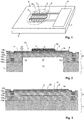
- batch 9 has a thickness of at least 5 ⁇ m, in particular between 6 and 15 ⁇ m.
- Recess 17 has a vertical depth of at least 1 ⁇ m, in particular of at least 3 ⁇ m.
Landscapes
- Chemical & Material Sciences (AREA)
- Physics & Mathematics (AREA)
- General Physics & Mathematics (AREA)
- Life Sciences & Earth Sciences (AREA)
- Health & Medical Sciences (AREA)
- Biochemistry (AREA)
- Analytical Chemistry (AREA)
- Pathology (AREA)
- Immunology (AREA)
- General Health & Medical Sciences (AREA)
- Chemical Kinetics & Catalysis (AREA)
- Electrochemistry (AREA)
- Engineering & Computer Science (AREA)
- Fluid Mechanics (AREA)
- Microelectronics & Electronic Packaging (AREA)
- Computer Hardware Design (AREA)
- Condensed Matter Physics & Semiconductors (AREA)
- Manufacturing & Machinery (AREA)
- Power Engineering (AREA)
- Measuring Volume Flow (AREA)
- Investigating Or Analyzing Materials By The Use Of Fluid Adsorption Or Reactions (AREA)
- Molecular Biology (AREA)
- Pressure Sensors (AREA)
Claims (19)
- Un dispositif capteur comprenant
un substrat semi-conducteur (1) ayant une surface supérieure (8) et une surface inférieure (7) et une ouverture (12) qui s'étend entre lesdites surfaces supérieure et inférieure (7, 8),
un groupe (9) de couches de matériau appliqué à ladite surface supérieure (8), une partie desdites couches de matériau dudit groupe (9) s'étendant au-dessus de ladite ouverture (12) pour former une membrane (13),
un chauffage (5) arrangé sur ladite membrane (13),
caractérisé en ce que ledit dispositif de capteur comprend une cavité (17) qui s'étend d'en bas à l'intérieur dudit groupe (9) de couches de matériau à un lieu de ladite membrane (13). - Le dispositif capteur selon la revendication 1, ladite cavité (17) ayant une profondeur d'au moins 1 µm, particulièrement d'au moins 3 µm.
- Le dispositif capteur selon l'une des revendications 1 ou 2, ladite cavité (17) ayant une surface de coupe transversale d'au moins 80 % d'une surface de coupe transversale d'une extrémité supérieure de ladite ouverture (12), et particulièrement ladite cavité (17) ayant une surface de coupe transversale égale à la surface de coupe transversale d'une extrémité supérieure de ladite ouverture (12).
- Le dispositif capteur selon l'une des revendications précédentes, ledit groupe (9) de couches de matériau comprenant une pluralité de couches (11) diélectriques structurées et une pluralité de couches (10a - 10f) métalliques structurées.
- Le dispositif capteur selon l'une des revendications précédentes, comprenant au moins une couche d'arrêt de gravure non-diélectrique (20) qui s'étend en forme d'anneau autour de ladite cavité (17), et particulièrement ledit anneau ayant une largeur (W) comprise entre 1 et 20 µm.
- Le dispositif capteur selon la revendication 5, ladite couche d'arrêt de gravure (20) étant en un matériau non-diélectrique, particulièrement en aluminium ou cuivre.
- Le dispositif capteur selon l'une des revendications précédentes, ladite membrane (13) comprenant au moins une couche de SiN (14) sous tension de traction.
- Le dispositif capteur selon l'une des revendications précédentes, comprenant
au moins un patch (2) d'un matériau de détection, particulièrement un oxyde de métal, arrangé sur ladite membrane (13) et
des électrodes (3) qui font du contact avec ledit matériau de détection, et particulièrement lesdites électrodes étant des électrodes métalliques. - Le dispositif capteur selon l'une des revendications précédentes, ledit chauffage (5) comprenant au moins un conducteur métallique, particulièrement un conducteur de tungstène.
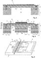
- Le dispositif capteur selon l'une des revendications précédentes, comprenant en outre des circuits de traitement (3) intégrés sur ledit substrat (1), et particulièrement lesdits circuits de traitement comprenant au moins un amplificateur, un convertisseur analogue-digital ou des circuits d'interface.
- Le dispositif capteur selon l'une des revendications précédentes, comprenant en outre une plaque de silicium (30) arrangée à un fond de ladite membrane (13), avec une fente (12b) formée autour de ladite plaque (30) entre ladite plaque (30) et ledit substrat (1), et particulièrement ledit substrat (1) étant une structure SOI ayant une couche de support de silicium (1a), une couche d'isolation (1b) et une couche de silicium (1c), ladite couche d'isolation (1b) étant arrangée entre ladite couche de support de silicium (1a) et ladite couche de silicium (1c).
- Le dispositif capteur selon l'une des revendications précédentes, ledit dispositif capteur étant un capteur de gaz ou un capteur d'humidité.
- Le dispositif capteur selon l'une des revendications 1 à 11, ledit dispositif capteur étant un capteur de flux comprenant au moins un, particulièrement au moins deux capteurs de température (31a, 31b) arrangés sur ladite membrane.
- Un procédé de fabrication d'un dispositif capteur, particulièrement le dispositif capteur selon l'une des revendications précédentes, comprenant les étapes
de fournir un substrat semi-conducteur (1) ayant une surface supérieure et une surface inférieure (7, 8),
d'appliquer un groupe (9) de couches de matériau à ladite surface supérieure (8) et de former un chauffage (5) dans ledit groupe (9) de couches de matériau,
de graver une ouverture (12) à travers ledit substrat (1) à partir de sa surface inférieure (8), par cela formant une membrane (13) à un lieu dudit chauffage (5),
caractérisé par l'étape
de former une cavité (17) dans ledit groupe (9) de couches de matériau en gravant à travers ladite ouverture (12), par cela réduisant une épaisseur de ladite membrane (13). - Le procédé selon la revendication 14, lesdites couches de matériau comprenant des couches diélectriques (11) et au moins une couche d'arrêt de gravure non-diélectrique (20), ladite couche d'arrêt de gravure (20) étant structurée pour s'étendre au-dessus d'un lieu de l'ouverture (12), ledit procédé comprenant l'étape d'utiliser ladite couche d'arrêt de gravure (20) comme arrêt de gravure pendant la formation de ladite cavité (17).
- Le procédé selon la revendication 15, comprenant en outre l'étape d'enlever au moins une partie de ladite couche d'arrêt de gravure (20) après avoir formé ladite cavité (17).
- Le procédé selon l'une des revendications 15 ou 16, au moins une première couche métallique (10a-10c) étant ajoutée audit groupe (9) de couches avant ladite couche d'arrêt de gravure (20) et au moins une deuxième couche métallique (10d - 10f) étant ajoutée audit groupe (9) de couches après la déposition de ladite couche d'arrêt de gravure (20).
- Le procédé selon l'une des revendications 15 à 17, comprenant en outre l'étape d'appliquer un patch (2) d'un matériau de détection à ladite membrane (13) après avoir gravé ladite cavité (17).
- Le procédé selon l'une des revendications 15 à 18, comprenant en outre l'étape de former une plaque de silicium (30) au-dessous de ladite membrane (13), une fente (12b) étant formée autour de ladite plaque (30) entre ladite plaque (30) et ledit substrat (1),
et particulièrement ledit substrat (1) étant une structure SOI ayant une couche de support de silicium (1a), une couche d'isolation (1b) et une couche de silicium (1c), ladite couche d'isolation (1b) étant arrangée entre ladite couche de support de silicium (1a) et ladite couche de silicium (1c), ladite plaque (30) étant formée de ladite couche de silicium (1c).
Priority Applications (3)
| Application Number | Priority Date | Filing Date | Title |
|---|---|---|---|
| EP13405014.5A EP2762864B1 (fr) | 2013-01-31 | 2013-01-31 | Dispositif de capteur à membrane et son procédé de fabrication |
| US14/161,267 US9224658B2 (en) | 2013-01-31 | 2014-01-22 | Membrane-based sensor device with non-dielectric etch-stop layer around substrate recess |
| CN201410056939.XA CN103969296B (zh) | 2013-01-31 | 2014-01-29 | 基于膜的传感器设备及其制造方法 |
Applications Claiming Priority (1)
| Application Number | Priority Date | Filing Date | Title |
|---|---|---|---|
| EP13405014.5A EP2762864B1 (fr) | 2013-01-31 | 2013-01-31 | Dispositif de capteur à membrane et son procédé de fabrication |
Publications (2)
| Publication Number | Publication Date |
|---|---|
| EP2762864A1 EP2762864A1 (fr) | 2014-08-06 |
| EP2762864B1 true EP2762864B1 (fr) | 2018-08-08 |
Family
ID=47877966
Family Applications (1)
| Application Number | Title | Priority Date | Filing Date |
|---|---|---|---|
| EP13405014.5A Active EP2762864B1 (fr) | 2013-01-31 | 2013-01-31 | Dispositif de capteur à membrane et son procédé de fabrication |
Country Status (3)
| Country | Link |
|---|---|
| US (1) | US9224658B2 (fr) |
| EP (1) | EP2762864B1 (fr) |
| CN (1) | CN103969296B (fr) |
Families Citing this family (18)
| Publication number | Priority date | Publication date | Assignee | Title |
|---|---|---|---|---|
| US9513242B2 (en) | 2014-09-12 | 2016-12-06 | Honeywell International Inc. | Humidity sensor |
| CN105590925B (zh) * | 2014-10-22 | 2019-03-01 | 日月光半导体制造股份有限公司 | 半导体封装结构及其制造方法 |
| US10945663B2 (en) | 2014-11-04 | 2021-03-16 | North Carolina State University | Smart sensing systems and related methods |
| DE102014226804A1 (de) * | 2014-12-22 | 2016-06-23 | Robert Bosch Gmbh | Verfahren zum Herstellen einer Gassensorvorrichtung zum Erfassen zumindest eines gasförmigen Analyten in einem Messmedium sowie Verfahren und Gassensorvorrichtung zum Erfassen zumindest eines gasförmigen Analyten in einem Messmedium |
| US10677747B2 (en) | 2015-02-17 | 2020-06-09 | Honeywell International Inc. | Humidity sensor |
| EP3062097A1 (fr) * | 2015-02-27 | 2016-08-31 | EM Microelectronic-Marin SA | Capteur d'humidité avec module thermique |
| GB2542801A (en) * | 2015-09-30 | 2017-04-05 | Cambridge Cmos Sensors Ltd | Micro gas sensor with a gas permeable region |
| DE102015225176A1 (de) * | 2015-12-15 | 2017-06-22 | Robert Bosch Gmbh | Mikromechanische Feststoffelektrolyt-Sensorvorrichtung |
| US10578572B2 (en) | 2016-01-19 | 2020-03-03 | Invensense, Inc. | CMOS integrated microheater for a gas sensor device |
| EP3244201B1 (fr) | 2016-05-13 | 2021-10-27 | Honeywell International Inc. | Capteur d'humidité à base de tec avec couche barrière protégeant le diélectrique de grille |
| US10488358B2 (en) * | 2016-05-31 | 2019-11-26 | Ams Sensors Uk Limited | Micro-hotplate devices with ring structures |
| CN106370247A (zh) * | 2016-09-06 | 2017-02-01 | 电子科技大学 | 一种基于聚合物的流量传感器及其制备方法 |
| CN109791117B (zh) | 2016-09-21 | 2022-09-20 | 盛思锐股份公司 | 气体传感器 |
| US10383967B2 (en) | 2016-11-30 | 2019-08-20 | Invensense, Inc. | Substance sensing with tracers |
| GB2558896B (en) * | 2017-01-17 | 2019-10-09 | Cambridge Entpr Ltd | A single membane flow-pressure sensing device |
| DE102017210585B3 (de) * | 2017-06-23 | 2018-09-27 | Robert Bosch Gmbh | Bondpadschichtsystem, Gassensor und Verfahren zur Herstellung eines Gassensors |
| CN107607152B (zh) * | 2017-07-18 | 2020-05-15 | 上海申矽凌微电子科技有限公司 | 传感器的制造方法及传感器 |
| TWI821853B (zh) * | 2022-01-05 | 2023-11-11 | 財團法人工業技術研究院 | 微機電感測裝置及其感測模組 |
Family Cites Families (34)
| Publication number | Priority date | Publication date | Assignee | Title |
|---|---|---|---|---|
| US3042786A (en) | 1958-08-14 | 1962-07-03 | American Brake Shoe Co | Electrical heating apparatus |
| US4651564A (en) | 1982-09-30 | 1987-03-24 | Honeywell Inc. | Semiconductor device |
| US5288147A (en) | 1992-11-09 | 1994-02-22 | Ta Instruments, Inc. | Thermopile differential thermal analysis sensor |
| DE4400838A1 (de) | 1994-01-14 | 1995-07-20 | Smt & Hybrid Gmbh | Gassensorchip und Verfahren zu dessen Herstellung |
| DE4418207C1 (de) | 1994-05-25 | 1995-06-22 | Siemens Ag | Thermischer Sensor/Aktuator in Halbleitermaterial |
| JP2880651B2 (ja) * | 1994-08-12 | 1999-04-12 | 東京瓦斯株式会社 | 熱式マイクロフローセンサ及びその製造方法 |
| GB9425931D0 (en) | 1994-12-22 | 1995-02-22 | Procter & Gamble | Cleansing compositions |
| US5656733A (en) | 1995-06-07 | 1997-08-12 | Hercules Incorporated | Lignin-containing resinous compositions |
| DE19610782B4 (de) * | 1996-03-19 | 2004-08-12 | Robert Bosch Gmbh | Verfahren zur Herstellung von mikromechanischen Strukturen |
| WO1997049998A1 (fr) | 1996-06-26 | 1997-12-31 | Simon Fraser University | Accelerometre sans masselottes |
| US6545334B2 (en) | 1997-12-19 | 2003-04-08 | Imec Vzw | Device and a method for thermal sensing |
| JP3470881B2 (ja) | 1999-04-19 | 2003-11-25 | 矢崎総業株式会社 | マイクロフローセンサ |
| JP4050857B2 (ja) | 1999-04-27 | 2008-02-20 | 矢崎総業株式会社 | 流体判別装置及び流量計測装置 |
| EP1065475B1 (fr) | 1999-05-31 | 2017-07-12 | Sensirion Holding AG | Procédé pour mesurer un courant de gaz |
| DE19928297A1 (de) * | 1999-06-22 | 2000-12-28 | Bosch Gmbh Robert | Verfahren zur Herstellung eines Sensors mit einer Membran |
| CH695166A5 (de) | 2000-04-25 | 2005-12-30 | Sensirion Ag | Verfahren und Vorrichtung zum Messen des Flusses einer Flüssigkeit. |
| JP2002048615A (ja) | 2000-08-02 | 2002-02-15 | Tokyo Gas Co Ltd | 熱フローセンサを用いた流量計 |
| US20040075140A1 (en) * | 2000-12-20 | 2004-04-22 | Henry Baltes | Microsensor and single chip integrated microsensor system |
| JP3658321B2 (ja) | 2000-12-28 | 2005-06-08 | オムロン株式会社 | フローセンサ及びその製造方法 |
| US7154372B2 (en) * | 2001-01-10 | 2006-12-26 | Sensirion Ag | Micromechanical flow sensor with tensile coating |
| US20030037590A1 (en) * | 2001-08-27 | 2003-02-27 | Stark Kevin C. | Method of self-testing a semiconductor chemical gas sensor including an embedded temperature sensor |
| JP3945385B2 (ja) | 2002-11-15 | 2007-07-18 | オムロン株式会社 | フローセンサ及び流量計測方法 |
| NL1025617C2 (nl) | 2003-05-13 | 2004-11-18 | Berkin Bv | Massadebietmeter. |
| DE602006019548D1 (de) | 2006-03-31 | 2011-02-24 | Sensirion Holding Ag | Durchflusssensor mit Thermoelementen |
| EP1840536B1 (fr) | 2006-03-31 | 2011-01-19 | Sensirion Holding AG | Débitmètre avec convertisseur analogique-numérique adaptable en fonction du débit |
| JP5031492B2 (ja) * | 2007-09-06 | 2012-09-19 | キヤノン株式会社 | インクジェットヘッド基板の製造方法 |
| KR100942439B1 (ko) * | 2007-12-28 | 2010-02-17 | 전자부품연구원 | 마이크로 가스센서 및 제조방법 |
| DE102009026021A1 (de) * | 2009-06-24 | 2010-12-30 | Saint-Gobain Sekurit Deutschland Gmbh & Co. Kg | Scheibe mit beheizbaren, optisch transparenten Sensorfeld |
| US20110138882A1 (en) * | 2009-12-11 | 2011-06-16 | Electronics And Telecommunications Research Institute | Semiconductor gas sensor having low power consumption |
| EP2348292A1 (fr) * | 2010-01-13 | 2011-07-27 | Sensirion AG | Dispositif capteur |
| CN102336390B (zh) * | 2010-07-26 | 2015-07-15 | 矽品精密工业股份有限公司 | 具有压力感测器的微机电结构及其制造方法 |
| US8907433B2 (en) * | 2012-09-28 | 2014-12-09 | Agilent Technologies, Inc. | Thin film with improved temperature range |
| EP2762866B1 (fr) * | 2013-01-31 | 2017-08-09 | Sensirion AG | Capteur de gaz CMOS et son procédé de fabrication |
| EP2762867B1 (fr) * | 2013-01-31 | 2018-11-21 | Sensirion AG | Capteur de gaz avec régulation de température |
-
2013
- 2013-01-31 EP EP13405014.5A patent/EP2762864B1/fr active Active
-
2014
- 2014-01-22 US US14/161,267 patent/US9224658B2/en active Active
- 2014-01-29 CN CN201410056939.XA patent/CN103969296B/zh active Active
Non-Patent Citations (1)
| Title |
|---|
| None * |
Also Published As
| Publication number | Publication date |
|---|---|
| EP2762864A1 (fr) | 2014-08-06 |
| US20140210036A1 (en) | 2014-07-31 |
| CN103969296B (zh) | 2019-07-26 |
| US9224658B2 (en) | 2015-12-29 |
| CN103969296A (zh) | 2014-08-06 |
Similar Documents
| Publication | Publication Date | Title |
|---|---|---|
| EP2762864B1 (fr) | Dispositif de capteur à membrane et son procédé de fabrication | |
| EP2762866B1 (fr) | Capteur de gaz CMOS et son procédé de fabrication | |
| KR100812996B1 (ko) | 마이크로 가스 센서 및 그 제조방법 | |
| EP2554981B1 (fr) | Circuit intégré avec un capteur de gaz et procédé de fabrication d'un tel circuit intégré | |
| KR20090064693A (ko) | 마이크로 가스 센서 및 그 제작 방법 | |
| US20070062812A1 (en) | Gas sensor and method for the production thereof | |
| US20070231942A1 (en) | Micromechanical flow sensor with tensile coating | |
| US10378989B2 (en) | Method for producing a sensor element by means of laser structuring | |
| KR20100053082A (ko) | 정전용량형 습도센서 및 그 제조방법 | |
| US10184777B2 (en) | Material damage system and method for determining same | |
| TWI630169B (zh) | 製造微機電系統裝置的方法 | |
| US20130126994A1 (en) | Capacitive pressure sensor and method for manufacturing same | |
| US20180340901A1 (en) | Gas sensor platform and the method of making the same | |
| CN104155035B (zh) | 压力传感器的形成方法 | |
| CN107827077A (zh) | 一种压阻式mems温度传感器及其制作方法 | |
| KR20050025383A (ko) | 센서 및 그 제조 방법 | |
| US11635401B2 (en) | Sensor device, method for manufacturing a sensor device and sensor assembly | |
| JP6340967B2 (ja) | ガスセンサ | |
| WO2007126269A1 (fr) | Capteur de pression capacitif fonctionnant en mode tactile | |
| US7059186B2 (en) | Integrated flow sensor for measuring a fluid flow | |
| US9130081B2 (en) | Bolometer having absorber with pillar structure for thermal shorting | |
| KR100504177B1 (ko) | 반도체 가스 센서 및 그 제조 방법 | |
| Chiang et al. | Capacitive absolute pressure sensor with independent electrode and membrane sizes for improved fractional capacitance change | |
| EP4332053A1 (fr) | Agencement de nanotubes de carbone et procédé de fabrication de l'agencement | |
| KR100489303B1 (ko) | 다이아몬드 필름 가스 센서 및 이의 제조방법 |
Legal Events
| Date | Code | Title | Description |
|---|---|---|---|
| PUAI | Public reference made under article 153(3) epc to a published international application that has entered the european phase |
Free format text: ORIGINAL CODE: 0009012 |
|
| 17P | Request for examination filed |
Effective date: 20130131 |
|
| AK | Designated contracting states |
Kind code of ref document: A1 Designated state(s): AL AT BE BG CH CY CZ DE DK EE ES FI FR GB GR HR HU IE IS IT LI LT LU LV MC MK MT NL NO PL PT RO RS SE SI SK SM TR |
|
| AX | Request for extension of the european patent |
Extension state: BA ME |
|
| R17P | Request for examination filed (corrected) |
Effective date: 20150113 |
|
| RBV | Designated contracting states (corrected) |
Designated state(s): AL AT BE BG CH CY CZ DE DK EE ES FI FR GB GR HR HU IE IS IT LI LT LU LV MC MK MT NL NO PL PT RO RS SE SI SK SM TR |
|
| STAA | Information on the status of an ep patent application or granted ep patent |
Free format text: STATUS: EXAMINATION IS IN PROGRESS |
|
| 17Q | First examination report despatched |
Effective date: 20161123 |
|
| GRAP | Despatch of communication of intention to grant a patent |
Free format text: ORIGINAL CODE: EPIDOSNIGR1 |
|
| STAA | Information on the status of an ep patent application or granted ep patent |
Free format text: STATUS: GRANT OF PATENT IS INTENDED |
|
| INTG | Intention to grant announced |
Effective date: 20180514 |
|
| GRAS | Grant fee paid |
Free format text: ORIGINAL CODE: EPIDOSNIGR3 |
|
| GRAA | (expected) grant |
Free format text: ORIGINAL CODE: 0009210 |
|
| STAA | Information on the status of an ep patent application or granted ep patent |
Free format text: STATUS: THE PATENT HAS BEEN GRANTED |
|
| AK | Designated contracting states |
Kind code of ref document: B1 Designated state(s): AL AT BE BG CH CY CZ DE DK EE ES FI FR GB GR HR HU IE IS IT LI LT LU LV MC MK MT NL NO PL PT RO RS SE SI SK SM TR |
|
| REG | Reference to a national code |
Ref country code: GB Ref legal event code: FG4D |
|
| REG | Reference to a national code |
Ref country code: CH Ref legal event code: EP Ref country code: AT Ref legal event code: REF Ref document number: 1027591 Country of ref document: AT Kind code of ref document: T Effective date: 20180815 |
|
| REG | Reference to a national code |
Ref country code: IE Ref legal event code: FG4D |
|
| REG | Reference to a national code |
Ref country code: DE Ref legal event code: R096 Ref document number: 602013041544 Country of ref document: DE |
|
| REG | Reference to a national code |
Ref country code: NL Ref legal event code: MP Effective date: 20180808 |
|
| REG | Reference to a national code |
Ref country code: LT Ref legal event code: MG4D |
|
| REG | Reference to a national code |
Ref country code: AT Ref legal event code: MK05 Ref document number: 1027591 Country of ref document: AT Kind code of ref document: T Effective date: 20180808 |
|
| PG25 | Lapsed in a contracting state [announced via postgrant information from national office to epo] |
Ref country code: SE Free format text: LAPSE BECAUSE OF FAILURE TO SUBMIT A TRANSLATION OF THE DESCRIPTION OR TO PAY THE FEE WITHIN THE PRESCRIBED TIME-LIMIT Effective date: 20180808 Ref country code: NO Free format text: LAPSE BECAUSE OF FAILURE TO SUBMIT A TRANSLATION OF THE DESCRIPTION OR TO PAY THE FEE WITHIN THE PRESCRIBED TIME-LIMIT Effective date: 20181108 Ref country code: RS Free format text: LAPSE BECAUSE OF FAILURE TO SUBMIT A TRANSLATION OF THE DESCRIPTION OR TO PAY THE FEE WITHIN THE PRESCRIBED TIME-LIMIT Effective date: 20180808 Ref country code: FI Free format text: LAPSE BECAUSE OF FAILURE TO SUBMIT A TRANSLATION OF THE DESCRIPTION OR TO PAY THE FEE WITHIN THE PRESCRIBED TIME-LIMIT Effective date: 20180808 Ref country code: GR Free format text: LAPSE BECAUSE OF FAILURE TO SUBMIT A TRANSLATION OF THE DESCRIPTION OR TO PAY THE FEE WITHIN THE PRESCRIBED TIME-LIMIT Effective date: 20181109 Ref country code: PL Free format text: LAPSE BECAUSE OF FAILURE TO SUBMIT A TRANSLATION OF THE DESCRIPTION OR TO PAY THE FEE WITHIN THE PRESCRIBED TIME-LIMIT Effective date: 20180808 Ref country code: IS Free format text: LAPSE BECAUSE OF FAILURE TO SUBMIT A TRANSLATION OF THE DESCRIPTION OR TO PAY THE FEE WITHIN THE PRESCRIBED TIME-LIMIT Effective date: 20181208 Ref country code: AT Free format text: LAPSE BECAUSE OF FAILURE TO SUBMIT A TRANSLATION OF THE DESCRIPTION OR TO PAY THE FEE WITHIN THE PRESCRIBED TIME-LIMIT Effective date: 20180808 Ref country code: BG Free format text: LAPSE BECAUSE OF FAILURE TO SUBMIT A TRANSLATION OF THE DESCRIPTION OR TO PAY THE FEE WITHIN THE PRESCRIBED TIME-LIMIT Effective date: 20181108 Ref country code: NL Free format text: LAPSE BECAUSE OF FAILURE TO SUBMIT A TRANSLATION OF THE DESCRIPTION OR TO PAY THE FEE WITHIN THE PRESCRIBED TIME-LIMIT Effective date: 20180808 Ref country code: LT Free format text: LAPSE BECAUSE OF FAILURE TO SUBMIT A TRANSLATION OF THE DESCRIPTION OR TO PAY THE FEE WITHIN THE PRESCRIBED TIME-LIMIT Effective date: 20180808 |
|
| PG25 | Lapsed in a contracting state [announced via postgrant information from national office to epo] |
Ref country code: AL Free format text: LAPSE BECAUSE OF FAILURE TO SUBMIT A TRANSLATION OF THE DESCRIPTION OR TO PAY THE FEE WITHIN THE PRESCRIBED TIME-LIMIT Effective date: 20180808 Ref country code: LV Free format text: LAPSE BECAUSE OF FAILURE TO SUBMIT A TRANSLATION OF THE DESCRIPTION OR TO PAY THE FEE WITHIN THE PRESCRIBED TIME-LIMIT Effective date: 20180808 Ref country code: HR Free format text: LAPSE BECAUSE OF FAILURE TO SUBMIT A TRANSLATION OF THE DESCRIPTION OR TO PAY THE FEE WITHIN THE PRESCRIBED TIME-LIMIT Effective date: 20180808 |
|
| PG25 | Lapsed in a contracting state [announced via postgrant information from national office to epo] |
Ref country code: EE Free format text: LAPSE BECAUSE OF FAILURE TO SUBMIT A TRANSLATION OF THE DESCRIPTION OR TO PAY THE FEE WITHIN THE PRESCRIBED TIME-LIMIT Effective date: 20180808 Ref country code: ES Free format text: LAPSE BECAUSE OF FAILURE TO SUBMIT A TRANSLATION OF THE DESCRIPTION OR TO PAY THE FEE WITHIN THE PRESCRIBED TIME-LIMIT Effective date: 20180808 Ref country code: CZ Free format text: LAPSE BECAUSE OF FAILURE TO SUBMIT A TRANSLATION OF THE DESCRIPTION OR TO PAY THE FEE WITHIN THE PRESCRIBED TIME-LIMIT Effective date: 20180808 Ref country code: RO Free format text: LAPSE BECAUSE OF FAILURE TO SUBMIT A TRANSLATION OF THE DESCRIPTION OR TO PAY THE FEE WITHIN THE PRESCRIBED TIME-LIMIT Effective date: 20180808 Ref country code: IT Free format text: LAPSE BECAUSE OF FAILURE TO SUBMIT A TRANSLATION OF THE DESCRIPTION OR TO PAY THE FEE WITHIN THE PRESCRIBED TIME-LIMIT Effective date: 20180808 |
|
| REG | Reference to a national code |
Ref country code: DE Ref legal event code: R097 Ref document number: 602013041544 Country of ref document: DE |
|
| PG25 | Lapsed in a contracting state [announced via postgrant information from national office to epo] |
Ref country code: SM Free format text: LAPSE BECAUSE OF FAILURE TO SUBMIT A TRANSLATION OF THE DESCRIPTION OR TO PAY THE FEE WITHIN THE PRESCRIBED TIME-LIMIT Effective date: 20180808 Ref country code: SK Free format text: LAPSE BECAUSE OF FAILURE TO SUBMIT A TRANSLATION OF THE DESCRIPTION OR TO PAY THE FEE WITHIN THE PRESCRIBED TIME-LIMIT Effective date: 20180808 Ref country code: DK Free format text: LAPSE BECAUSE OF FAILURE TO SUBMIT A TRANSLATION OF THE DESCRIPTION OR TO PAY THE FEE WITHIN THE PRESCRIBED TIME-LIMIT Effective date: 20180808 |
|
| PLBE | No opposition filed within time limit |
Free format text: ORIGINAL CODE: 0009261 |
|
| STAA | Information on the status of an ep patent application or granted ep patent |
Free format text: STATUS: NO OPPOSITION FILED WITHIN TIME LIMIT |
|
| 26N | No opposition filed |
Effective date: 20190509 |
|
| PG25 | Lapsed in a contracting state [announced via postgrant information from national office to epo] |
Ref country code: SI Free format text: LAPSE BECAUSE OF FAILURE TO SUBMIT A TRANSLATION OF THE DESCRIPTION OR TO PAY THE FEE WITHIN THE PRESCRIBED TIME-LIMIT Effective date: 20180808 Ref country code: MC Free format text: LAPSE BECAUSE OF FAILURE TO SUBMIT A TRANSLATION OF THE DESCRIPTION OR TO PAY THE FEE WITHIN THE PRESCRIBED TIME-LIMIT Effective date: 20180808 |
|
| PG25 | Lapsed in a contracting state [announced via postgrant information from national office to epo] |
Ref country code: LU Free format text: LAPSE BECAUSE OF NON-PAYMENT OF DUE FEES Effective date: 20190131 |
|
| REG | Reference to a national code |
Ref country code: BE Ref legal event code: MM Effective date: 20190131 |
|
| REG | Reference to a national code |
Ref country code: IE Ref legal event code: MM4A |
|
| PG25 | Lapsed in a contracting state [announced via postgrant information from national office to epo] |
Ref country code: BE Free format text: LAPSE BECAUSE OF NON-PAYMENT OF DUE FEES Effective date: 20190131 |
|
| PG25 | Lapsed in a contracting state [announced via postgrant information from national office to epo] |
Ref country code: IE Free format text: LAPSE BECAUSE OF NON-PAYMENT OF DUE FEES Effective date: 20190131 |
|
| PG25 | Lapsed in a contracting state [announced via postgrant information from national office to epo] |
Ref country code: TR Free format text: LAPSE BECAUSE OF FAILURE TO SUBMIT A TRANSLATION OF THE DESCRIPTION OR TO PAY THE FEE WITHIN THE PRESCRIBED TIME-LIMIT Effective date: 20180808 |
|
| PG25 | Lapsed in a contracting state [announced via postgrant information from national office to epo] |
Ref country code: PT Free format text: LAPSE BECAUSE OF FAILURE TO SUBMIT A TRANSLATION OF THE DESCRIPTION OR TO PAY THE FEE WITHIN THE PRESCRIBED TIME-LIMIT Effective date: 20181208 Ref country code: MT Free format text: LAPSE BECAUSE OF NON-PAYMENT OF DUE FEES Effective date: 20190131 |
|
| PG25 | Lapsed in a contracting state [announced via postgrant information from national office to epo] |
Ref country code: CY Free format text: LAPSE BECAUSE OF FAILURE TO SUBMIT A TRANSLATION OF THE DESCRIPTION OR TO PAY THE FEE WITHIN THE PRESCRIBED TIME-LIMIT Effective date: 20180808 |
|
| PG25 | Lapsed in a contracting state [announced via postgrant information from national office to epo] |
Ref country code: HU Free format text: LAPSE BECAUSE OF FAILURE TO SUBMIT A TRANSLATION OF THE DESCRIPTION OR TO PAY THE FEE WITHIN THE PRESCRIBED TIME-LIMIT; INVALID AB INITIO Effective date: 20130131 |
|
| PG25 | Lapsed in a contracting state [announced via postgrant information from national office to epo] |
Ref country code: MK Free format text: LAPSE BECAUSE OF FAILURE TO SUBMIT A TRANSLATION OF THE DESCRIPTION OR TO PAY THE FEE WITHIN THE PRESCRIBED TIME-LIMIT Effective date: 20180808 |
|
| P01 | Opt-out of the competence of the unified patent court (upc) registered |
Effective date: 20230602 |
|
| PGFP | Annual fee paid to national office [announced via postgrant information from national office to epo] |
Ref country code: DE Payment date: 20240119 Year of fee payment: 12 Ref country code: GB Payment date: 20240124 Year of fee payment: 12 Ref country code: CH Payment date: 20240201 Year of fee payment: 12 |
|
| PGFP | Annual fee paid to national office [announced via postgrant information from national office to epo] |
Ref country code: FR Payment date: 20240123 Year of fee payment: 12 |