EP2762864B1 - Membrane-based sensor device and method for manufacturing the same - Google Patents
Membrane-based sensor device and method for manufacturing the same Download PDFInfo
- Publication number
- EP2762864B1 EP2762864B1 EP13405014.5A EP13405014A EP2762864B1 EP 2762864 B1 EP2762864 B1 EP 2762864B1 EP 13405014 A EP13405014 A EP 13405014A EP 2762864 B1 EP2762864 B1 EP 2762864B1
- Authority
- EP
- European Patent Office
- Prior art keywords
- sensor device
- layer
- membrane
- batch
- recess
- Prior art date
- Legal status (The legal status is an assumption and is not a legal conclusion. Google has not performed a legal analysis and makes no representation as to the accuracy of the status listed.)
- Active
Links
Images
Classifications
-
- H—ELECTRICITY
- H01—ELECTRIC ELEMENTS
- H01L—SEMICONDUCTOR DEVICES NOT COVERED BY CLASS H10
- H01L21/00—Processes or apparatus adapted for the manufacture or treatment of semiconductor or solid state devices or of parts thereof
- H01L21/70—Manufacture or treatment of devices consisting of a plurality of solid state components formed in or on a common substrate or of parts thereof; Manufacture of integrated circuit devices or of parts thereof
- H01L21/77—Manufacture or treatment of devices consisting of a plurality of solid state components or integrated circuits formed in, or on, a common substrate
- H01L21/78—Manufacture or treatment of devices consisting of a plurality of solid state components or integrated circuits formed in, or on, a common substrate with subsequent division of the substrate into plural individual devices
- H01L21/82—Manufacture or treatment of devices consisting of a plurality of solid state components or integrated circuits formed in, or on, a common substrate with subsequent division of the substrate into plural individual devices to produce devices, e.g. integrated circuits, each consisting of a plurality of components
- H01L21/84—Manufacture or treatment of devices consisting of a plurality of solid state components or integrated circuits formed in, or on, a common substrate with subsequent division of the substrate into plural individual devices to produce devices, e.g. integrated circuits, each consisting of a plurality of components the substrate being other than a semiconductor body, e.g. being an insulating body
-
- G—PHYSICS
- G01—MEASURING; TESTING
- G01F—MEASURING VOLUME, VOLUME FLOW, MASS FLOW OR LIQUID LEVEL; METERING BY VOLUME
- G01F1/00—Measuring the volume flow or mass flow of fluid or fluent solid material wherein the fluid passes through a meter in a continuous flow
- G01F1/68—Measuring the volume flow or mass flow of fluid or fluent solid material wherein the fluid passes through a meter in a continuous flow by using thermal effects
- G01F1/684—Structural arrangements; Mounting of elements, e.g. in relation to fluid flow
- G01F1/6845—Micromachined devices
-
- G—PHYSICS
- G01—MEASURING; TESTING
- G01N—INVESTIGATING OR ANALYSING MATERIALS BY DETERMINING THEIR CHEMICAL OR PHYSICAL PROPERTIES
- G01N27/00—Investigating or analysing materials by the use of electric, electrochemical, or magnetic means
- G01N27/02—Investigating or analysing materials by the use of electric, electrochemical, or magnetic means by investigating impedance
- G01N27/04—Investigating or analysing materials by the use of electric, electrochemical, or magnetic means by investigating impedance by investigating resistance
- G01N27/12—Investigating or analysing materials by the use of electric, electrochemical, or magnetic means by investigating impedance by investigating resistance of a solid body in dependence upon absorption of a fluid; of a solid body in dependence upon reaction with a fluid, for detecting components in the fluid
- G01N27/128—Microapparatus
-
- G—PHYSICS
- G01—MEASURING; TESTING
- G01N—INVESTIGATING OR ANALYSING MATERIALS BY DETERMINING THEIR CHEMICAL OR PHYSICAL PROPERTIES
- G01N27/00—Investigating or analysing materials by the use of electric, electrochemical, or magnetic means
- G01N27/02—Investigating or analysing materials by the use of electric, electrochemical, or magnetic means by investigating impedance
- G01N27/04—Investigating or analysing materials by the use of electric, electrochemical, or magnetic means by investigating impedance by investigating resistance
- G01N27/14—Investigating or analysing materials by the use of electric, electrochemical, or magnetic means by investigating impedance by investigating resistance of an electrically-heated body in dependence upon change of temperature
Definitions
- batch 9 has a thickness of at least 5 ⁇ m, in particular between 6 and 15 ⁇ m.
- Recess 17 has a vertical depth of at least 1 ⁇ m, in particular of at least 3 ⁇ m.
Description
- The invention relates to a sensor device having a semiconductor substrate with an opening, a membrane extending over said opening and a heater located on the membrane. The invention also relates to a method for manufacturing such a sensor device.
- Various sensor devices require a heater. One group of such devices is formed by flow sensors, where changes in the thermal distribution around the heater are used to measure a fluid flow. Such a device is e.g. disclosed in
US 2007/0241093 . Another group of such devices comprises gas sensors, where the heater is used to heat a sensing material, such as a metal oxide, to an operating temperature. A device using such a hot plate is e.g. disclosed inWO 95/19563 - This type of devices can be integrated onto a semiconductor substrate, in which case, the heater is advantageously arranged on a membrane over an opening in the semiconductor substrate, thereby reducing the thermal loss as compared to devices where the heater is arranged over the bulk of the substrate material. Arranging the heater on a membrane has a series of advantages, such as reducing power consumption, increasing sensitivity and reducing the time required for switching on the device.
-
EP 0 696 725 A1 introduces a thermal micro flow sensor including a heating wire, said heating wire being made of a material like polysilicon so that said heating wire has a resistance about 1 kΩ, said heating wire being formed on a semiconductor substrate so that said heating wire has a thermal isolation structure for isolating said heating wire from said semiconductor substrate. Underneath the heating wire a recess is etched into the semiconductor substrate from its front side by means of etching holes thereby forming an undercut thereby thermally isolating the heating wire from the silicon substrate. - It is an object of the present invention to provide an improved design and manufacturing method for such a sensor that has low thermal losses through the membrane.
- This object is achieved by the sensor device and the method of the independent claims.
- Accordingly, the sensor device comprises a semiconductor substrate (such as a silicon substrate) having a top and a bottom surface and an opening extending between the top and bottom surfaces. A batch of material layers, e.g. comprising structured dielectric and metallic or semiconducting layers, is arranged on the top surface of the substrate, e.g. in order to form conducting leads and other electrical and electronic components of the device. Some of the material layers extend over the opening of the semiconductor substrate, thereby forming a membrane. Further, a heater is arranged on the membrane.
- In addition, the device comprises a recess extending from below into the batch of material layers at the location of the membrane, thereby reducing the thickness of the membrane and therefore thermal losses through the membrane.
- A device of this type can be manufactured by providing a semiconductor substrate having a top and a bottom surface. The mentioned batch of material layers is applied to the top surface, and a heater is formed in the batch of material layers by suitable structuring techniques. Further, an opening is etched through the substrate, thereby forming a membrane formed by the material layers at the location of the heater. In addition, a recess is etched into the bottom side of the batch of material layers, namely by applying an etching agent through the opening in the substrate. In this manner, the thickness of the membrane is reduced.
- This design is particularly advantageous when being combined with modern CMOS processes, where typically a very large batch of material layers is applied to the semiconductor substrate. This batch can have a thickness of 10 µm or more, even at locations where the metal layers are removed. By forming said recess in the membrane, the thickness of the membrane can be optimized.
- Etching the recess from below has the further advantage that it does not affect the topography of the top surface of the batch of material layers, while forming the recess from above would lead to a non-flat surface of the membrane, which would render the formation of electrode structures and of other type of surface structures more difficult, in particular when using photolithography.
- Typically, the batch of material layers comprises a plurality of structured dielectric layers and a plurality of structured metal layers, such as e.g. known from conventional CMOS devices. It can e.g. be manufactured by subsequent application of unstructured layers of suitable materials and structuring the same using photolithographic techniques.
- Further, the batch of material layers advantageously comprises at least one non-dielectric etch-stop layer, which is structured to extend over the location of the opening to be formed in the substrate. This etch-stop layer is used as an etch-stop when forming the recess into the batch of material layers. Even though the etch-stop layer is not strictly necessary (timed etching could be used instead in order to etch the recess to a certain depth), it is advantageous since it allows to stop the etching-process at a well-defined location.
- After etching the recess, at least part of the etch-stop layer should be removed in order to further reduce the thermal conductivity of the membrane.
- The sensor is advantageously a gas sensor or a flow sensor.
- Other advantageous embodiments are listed in the dependent claims as well as in the description below.
- The invention will be better understood and objects other than those set forth above will become apparent from the following detailed description thereof. Such description makes reference to the annexed drawings, wherein:
-
Fig. 1 shows a view of a sensor device, -
Fig. 2 shows a sectional view of the device, -
Fig. 3 shows a sectional view of the device after forming the batch of material layers, -
Fig. 4 shows a sectional view of the device after forming the recess, -
Fig. 5 shows a second embodiment of the device with a silicon plate arranged at the bottom of the membrane, and -
Fig. 6 shows a view of a flow sensor. - Terms indicating a vertical direction or arrangement, such as "top", "bottom", "above" or "below" relate to a frame of reference where the batch of material layers forming the membrane are arranged on top, i.e. above, the substrate. In other words, the substrate is arranged, by definition, below the material layers and the membrane is located on top of the opening extending through the substrate.
- The term "lateral" is used to describe directions parallel to the top and bottom surfaces of the semiconductor substrate.
- A "dielectric" material is a non-conductive, non-metallic material, in particular an oxide or nitride, such as SiO2 or SiN.
- A "non-dielectric" material is a metal or a metalloid.
- An "SOI-structure" ("Silicon on Insulator") is a structure comprising a handle substrate of silicon, a silicon layer, and an insulator layer arranged between the handle substrate and the silicon layer.
-
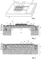
Fig. 1 shows a gas sensor adapted to generate a signal indicative of the concentration of at least one gaseous analyte in a gaseous carrier, such as alcohol in air. It comprises asemiconductor substrate 1. A sensor material, whose electrical properties depend on the concentration of the analyte, is applied tosubstrate 1 in a patch 2. For example, patch 2 consists of a granular layer of SnO, whose electrical resistance depends on the presence and concentration of various compounds in the surrounding atmosphere. This type of device is e.g. described byWO 95/19563 interdigital metal electrodes 3, which are connected toprocessing circuitry 4.Processing circuitry 4 is integrated onsemiconductor substrate 1 and can e.g. comprise active components, such as transistors, at least one amplifier, at least one analog/digital converter, and/or interface circuitry, etc. - The sensor device further comprises a
heater 5 positioned at the location of patch 2 in order to heat patch 2 to its operating temperature, which, for SnO, is e.g. typically at least 300°C. -
Fig. 2 shows a sectional view of this type of device. As can be seen,semiconductor substrate 1 comprises a bottom surface 7 (cf.Fig. 1 ) and atop surface 8. Abatch 9 of material layers is applied totop surface 8 and typically comprises a plurality of structured dielectric layers and a plurality of structured metal layers as used in standard CMOS processes. - Typically, the metal layers, which are generally designated by
reference numbers 10a - 10f, are of aluminum or copper, and they are structured to form leads and other electrical components. InFig. 2 , they are only shown schematically. The metal layers 10a - 10f are separated by dielectric layers, typically SiO2 layers, which are generally denoted byreference number 11. - Part of the layers of
batch 9 extend over anopening 12 insemiconductor substrate 1 and form amembrane 13.Membrane 13 can have circular or rectangular cross section or any other suitable cross-section. - Advantageously, and in order to reduce the thermal conductance of
membrane 13, none of the aluminum orcopper metal layers 10a - 10f extends intomembrane 13. -
Batch 9 further comprises alayer 14 of SiN under tensile stress, which extends at least overmembrane 13 and is anchored laterally outsidemembrane 13. The tensile stress inlayer 14 is at least sufficiently large to exceed the compressive stress in therest membrane 13, which leads to a total tensile stress in the membrane. As described inUS 7 154 372 , such a tensile layer can be used to prevent the membrane from buckling. -
Heater 5 is formed by structuring a metal layer into at least one metal conductor, which is located onmembrane 13. Advantageously,heater 5 is formed by a tungsten conductor. As seen inFig 1 , the metal conductor can e.g. follow a meandering path. The layer ofheater 5 is arranged onSiN layer 14. - A SiO2 layer 15 is arranged on top of the layer of
heater 5 and electrically insulates the same from a further metal layer forming theelectrodes 3. - A protective dielectric layer can be applied to the top of the device (not shown).
- As can be seen in
Fig. 2 , at the location of the membrane the device further comprises arecess 17 extending from below into thebatch 9 of material layers. This recess has the purpose, as discussed above, to reduce the thickness ofmembrane 13. - Typically,
batch 9 has a thickness of at least 5 µm, in particular between 6 and 15 µm.Recess 17 has a vertical depth of at least 1 µm, in particular of at least 3 µm. - The cross section, i.e. the lateral extension, of
recess 17 is advantageously equal to the cross section of the upper end of opening 12, such that it spans the whole membrane, and the membrane therefore has a reduced thickness everywhere. Alternatively, the cross section area ofrecess 17 should be at least 80% of the cross section area of the upper end ofopening 12. -
Membrane 13 should have sufficiently large lateral extensions to provide a thermally insulated location for receiving patch 2. Advantageously,membrane 13 should cover an area of at least 0.1 mm2, in particular at least 0.2 mm2. - For reasons that will become apparent from the description of the manufacturing process below, the sensor device further comprises at least one etch-
stop layer 20, or, rather, residual remains thereof, arranged in a ring aroundrecess 17. Etch-stop layer 20 is of a non-dielectric material, in particular of aluminum or copper. The ring of etch-stop layer 20 has a lateral width W between 1 - 20 µm in order to be able to compensate for positioning errors in the etching process described below. The shape of the ring formed by edge-stop layer 20 depends on the shape ofrecess 17. - As can be seen, etch-
stop layer 20 is advantageously positioned at a height between two of themetal layers 10a - 10f, i.e. at an intermediate height ofbatch 9, namely at such a height that the distance between etch-stop layer 20 and the top ofbatch 9 corresponds to the desired thickness of the membrane. -
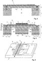
Figs. 3 and4 show a method for manufacturing the sensor device. - In a first step,
silicon substrate 1 is covered, at its top surface, with thedielectric layers 11 as well as with themetal layers 10a - 10f in a series of steps as known in the art of semiconductor device manufacture. For example, a first SiO2-layer is applied totop surface 8, then thefirst metal layer 10a is applied onto the first SiO2-layer and structured using photolithography. Then, a second SiO2-layer is applied, and thesecond metal layer 10b is applied thereto and structured, etc. - Between two of these steps, etch-
stop layer 20 is applied and structured to extend over the area offuture opening 12 and slightly beyond. For the reasons mentioned above, at least one first metal layer (in the embodiment ofFig. 3 themetal layers 10a - 10c) is added tobatch 9 of layers before etch-stop 20 layer is formed, and at least one second metal layer (10d - 10f) is added tobatch 9 of layers after etch-stop layer 20 is formed. - After applying the
metal layers 10a - 10f, etch-stop layer 20 and thedielectric layers 11, the layer forheater 5 is applied and structured, followed by the application oftensile layer 15 and theelectrodes 3. This results in a device as shown inFig. 3 . - In a next step, opening 12 is etched out from the bottom side 7 of
semiconductor substrate 1, e.g. using a plasma-process (such as deep reactive ion etching) or a wet process (such as anisotropic etching using KOH) after application of a photolithographic mask to bottom side 7. This step uses the bottom surface of thedielectric layers 11 as an etch-stop. - In a next step,
recess 17 is etched. In this step, etch-stop layer 20 acts as an etch-stop. Ifrecess 17 is to have the same lateral extension as opening 12, no masking is required in this step. - The resulting device is shown in
Fig. 4 . - In a next step, the accessible part of etch-
stop layer 20 can optionally be removed by etching. A residual ring of the etch-stop layer 20 of widthW surround recess 17, as described above, remains in the device. - Now, patch 2 of the sensing material can be applied to the top of
membrane 13. -
Fig. 5 shows an alternative design of the device with a silicon plate 30 arranged at the bottom ofmembrane 13. Silicon plate 30 is not connected tosubstrate 1, i.e. there is a gap between silicon plate 30 andsubstrate 1, which extends all around silicon plate 30 and is formed by opening 12 andrecess 17.Recess 17 has annular shape. - The purpose of silicon plate 30 is to provide a uniform temperature distribution at the location of patch 2.
- Plate 30 can have a thickness equal to
substrate 1, in which case the device can be manufactured as described above with the sole difference that opening 12 has annular shape, thereby forming plate 30 fromsubstrate 1. - Alternatively, and as shown in
Fig. 5 , plate 30 can have a thickness smaller than the thickness ofsubstrate 1. To manufacture a sensor of this type,substrate 1 can be formed by an SOI structure. In other words, an SOI-wafer is used formanufacturing substrate 1. Such an SOI-waver comprises ahandle substrate 1a, an insulatinglayer 1b (in particular SiO2) arranged onsubstrate 1a, and amonocrystalline silicon layer 1c on top of insulatinglayer 1b. Typically, the thickness ofsilicon layer 1c is much smaller than the thickness ofhandle substrate 1a. This type of SOI-waver is known to the skilled person. - The batch of
layers 9 is integrated on top ofsilicon layer 1c. - For
manufacturing opening 12 andrecess 17, the device is again etched from its bottom side. In a first step, afirst part 12a of opening 12 is formed, using insulatinglayer 1b as an etch stop. A mask is then applied on insulatinglayer 1b at the location of the future plate 30, and insulatinglayer 1b is removed outside this mask. Then, an annularsecond part 12b of opening 12 is formed by etching offsilicon layer 1c where it is not masked, thereby forming plate 30 fromsilicon layer 1c.Second part 12b forms the annular gap extending all around plate 30 between plate 30 andsubstrate 1. Finally,recess 17 is formed by etching from the sidesecond part 12b of opening 12 as described above. - As mentioned, the sensor device can also be a thermal flow sensor, e.g. of the type described in
US 2007/0241093 , which has a heater arranged on the membrane. A fluid flowing over the membrane distorts the thermal field generated by the heater, which in turn can be detected by one or more suitable temperature sensors arranged on the membrane. -
Fig. 6 shows such a flow sensor having anelongate heater 5 arranged onmembrane 13, as well as at least one, in particular twotemperature sensors 31a, 31b onmembrane 13. The twotemperature sensors 31a, 31b are arranged on both sides (upstream and downstream) ofheater 5. Thetemperature sensors 31a, 31b in the shown embodiment are thermopiles, as described inUS 2007/0241093 . The device can be used to measure a flow F in a direction perpendicular to the elongate axis ofheater 5. - In the embodiment described in reference to
Figs. 1 - 5 , the sensor device was a gas sensor having a metal oxide, in particular SnO, as sensing material. The device can, however, also be a gas sensor using another sensing material as known to the skilled person. - The sensor device may also be any other type of device where a heater is arranged on a thin membrane.
- While there are shown and described presently preferred embodiments of the invention, it is to be distinctly understood that the invention is not limited thereto but may be otherwise variously embodied and practised within the scope of the following claims.
Claims (19)
- A sensor device comprising
a semiconductor substrate (1) having a top (8) and a bottom (7) surface and an opening (12) extending between said top and bottom surfaces (7, 8),
a batch (9) of material layers applied to said top surface (8), wherein part of said material layers of said batch (9) extend over said opening (12) for forming a membrane (13),
a heater (5) arranged on said membrane (13),
characterized in that said sensor device comprises a recess (17) extending from below into said batch (9) of material layers at a location of said membrane (13). - The sensor device of claim 1 wherein said recess (17) has a depth of at least 1 µm, in particular of at least 3 µm.
- The sensor device of any of the claims 1 or 2 wherein said recess (17) has a cross section area of at least 80% of a cross section area of an upper end of said opening (12), and in particular wherein said recess (17) has a cross section equal to the cross section of the upper end of said opening (12).
- The sensor device of any of the preceding claims wherein said batch (9) of material layers comprises a plurality of structured dielectric layers (11) and a plurality of structured metal layers (10a -10f).
- The sensor device of any of the preceding claims further comprising at least one non-dielectric etch-stop layer (20) extending in a ring around said recess (17), and in particular wherein said ring has a width (W) between 1 and 20 µm
- The sensor device of claim 5 wherein said etch-stop layer (20) is of a non-dielectric material, in particular of aluminum or copper.
- The sensor device of any of the preceding claims wherein said membrane (13) comprises at least one SiN-layer (14) under tensile stress.
- The sensor device of any of the preceding claims further comprising
at least one patch (2) of a sensing material, in particular a metal oxide, arranged on said membrane (13) and
electrodes (3) contacting said sensing material, and in particular wherein said electrodes are metal electrodes. - The sensor device of any of the preceding claims wherein said heater (5) comprises at least one metal conductor, in particular a tungsten conductor.
- The sensor device of any of the preceding claims further comprising processing circuitry (3) integrated on said substrate (1), and in particular wherein said processing circuitry comprises at least one amplifier, analog/digital-converter or interface circuitry.
- The sensor device of any of the preceding claims further comprising a silicon plate (30) arranged at a bottom of said membrane (13), with a gap (12b) formed around said plate (30) between said plate (30) and said substrate (1), and in particular wherein said substrate (1) is an SOI structure having a silicon handle layer (1a), an insulating layer (1b) and a silicon layer (1c), with said insulating layer (1b) arranged between said silicon handle layer (1a) and said silicon layer (1c) .
- The sensor device of any of the preceding claims, wherein said sensor device is a gas sensor or a humidity sensor.
- The sensor device of any of the claims 1 to 11 wherein said sensor device is a flow sensor comprising at least one, in particular at least two temperature sensors (31a, 31b) arranged on said membrane.
- A method for manufacturing a sensor device, in particular the sensor device of any of the preceding claims, comprising the steps of
providing a semiconductor substrate (1) having a top and a bottom surface (7, 8),
applying a batch (9) of material layers to said top surface (8) and forming a heater (5) in said batch (9) of material layers,
etching an opening (12) through said substrate (1) from its bottom surface (8), thereby forming a membrane (13) at a location of said heater (5),
characterized by the step of
forming a recess (17) in said batch (9) of material layers by etching through said opening (12) thereby reducing a thickness of said membrane (13). - The method of claim 14 wherein said material layers comprise dielectric layers (11) and at least one non-dielectric etch-stop layer (20), wherein said etch-stop layer (20) is structured to extend over a location of the opening (12), wherein said method comprises the step using said etch-stop layer (20) as an etch-stop when forming said recess (17).
- The method of claim 15 further comprising the step of removing at least part of said etch-stop layer (20) after forming said recess (17).
- The method of any of the claims 15 or 16 wherein at least one first metal layer (10a - 10c) is added to said batch (9) of layers before said etch-stop layer (20) and at least one second metal layer (10d-10f) is added to said batch (9) of layers after deposition of said etch-stop layer (20).
- The method of any of the claims 15 to 17 further comprising the step of applying a patch (2) of a sensing material to said membrane (13) after etching said recess (17).
- The method of any of the claims 15 to 18 further comprising the step of forming a silicon plate (30) below said membrane (13), with a gap (12b) formed around said plate (30) between said plate (30) and said substrate (1),
and in particular wherein said substrate (1) is an SOI structure having a silicon handle layer (1a), an insulating layer (1b) and a silicon layer (1c), with said insulating layer (1b) arranged between said silicon handle layer (1a) and said silicon layer (1c), wherein said plate (30) is formed from said silicon layer (1c).
Priority Applications (3)
| Application Number | Priority Date | Filing Date | Title |
|---|---|---|---|
| EP13405014.5A EP2762864B1 (en) | 2013-01-31 | 2013-01-31 | Membrane-based sensor device and method for manufacturing the same |
| US14/161,267 US9224658B2 (en) | 2013-01-31 | 2014-01-22 | Membrane-based sensor device with non-dielectric etch-stop layer around substrate recess |
| CN201410056939.XA CN103969296B (en) | 2013-01-31 | 2014-01-29 | Sensor device and its manufacturing method based on film |
Applications Claiming Priority (1)
| Application Number | Priority Date | Filing Date | Title |
|---|---|---|---|
| EP13405014.5A EP2762864B1 (en) | 2013-01-31 | 2013-01-31 | Membrane-based sensor device and method for manufacturing the same |
Publications (2)
| Publication Number | Publication Date |
|---|---|
| EP2762864A1 EP2762864A1 (en) | 2014-08-06 |
| EP2762864B1 true EP2762864B1 (en) | 2018-08-08 |
Family
ID=47877966
Family Applications (1)
| Application Number | Title | Priority Date | Filing Date |
|---|---|---|---|
| EP13405014.5A Active EP2762864B1 (en) | 2013-01-31 | 2013-01-31 | Membrane-based sensor device and method for manufacturing the same |
Country Status (3)
| Country | Link |
|---|---|
| US (1) | US9224658B2 (en) |
| EP (1) | EP2762864B1 (en) |
| CN (1) | CN103969296B (en) |
Families Citing this family (18)
| Publication number | Priority date | Publication date | Assignee | Title |
|---|---|---|---|---|
| US9513242B2 (en) | 2014-09-12 | 2016-12-06 | Honeywell International Inc. | Humidity sensor |
| CN105590925B (en) * | 2014-10-22 | 2019-03-01 | 日月光半导体制造股份有限公司 | Semiconductor package and its manufacturing method |
| US10945663B2 (en) | 2014-11-04 | 2021-03-16 | North Carolina State University | Smart sensing systems and related methods |
| DE102014226804A1 (en) * | 2014-12-22 | 2016-06-23 | Robert Bosch Gmbh | Method for producing a gas sensor device for detecting at least one gaseous analyte in a measuring medium and method and gas sensor device for detecting at least one gaseous analyte in a measuring medium |
| WO2016134079A1 (en) | 2015-02-17 | 2016-08-25 | Honeywell International Inc. | Humidity sensor and method for manufacturing the sensor |
| EP3062097A1 (en) * | 2015-02-27 | 2016-08-31 | EM Microelectronic-Marin SA | Moisture sensor with thermal module |
| GB2542801A (en) * | 2015-09-30 | 2017-04-05 | Cambridge Cmos Sensors Ltd | Micro gas sensor with a gas permeable region |
| DE102015225176A1 (en) * | 2015-12-15 | 2017-06-22 | Robert Bosch Gmbh | Micromechanical solid electrolyte sensor device |
| US10578572B2 (en) * | 2016-01-19 | 2020-03-03 | Invensense, Inc. | CMOS integrated microheater for a gas sensor device |
| EP3244201B1 (en) | 2016-05-13 | 2021-10-27 | Honeywell International Inc. | Fet based humidity sensor with barrier layer protecting gate dielectric |
| US10488358B2 (en) * | 2016-05-31 | 2019-11-26 | Ams Sensors Uk Limited | Micro-hotplate devices with ring structures |
| CN106370247A (en) * | 2016-09-06 | 2017-02-01 | 电子科技大学 | Flow sensor based on polymer and preparation method of flow sensor |
| CH714339B1 (en) | 2016-09-21 | 2020-06-30 | Sensirion Ag | Gas sensor. |
| US10383967B2 (en) | 2016-11-30 | 2019-08-20 | Invensense, Inc. | Substance sensing with tracers |
| GB2558896B (en) * | 2017-01-17 | 2019-10-09 | Cambridge Entpr Ltd | A single membane flow-pressure sensing device |
| DE102017210585B3 (en) * | 2017-06-23 | 2018-09-27 | Robert Bosch Gmbh | Bondpad layer system, gas sensor and method for producing a gas sensor |
| CN107607152B (en) * | 2017-07-18 | 2020-05-15 | 上海申矽凌微电子科技有限公司 | Method for manufacturing sensor and sensor |
| TWI821853B (en) * | 2022-01-05 | 2023-11-11 | 財團法人工業技術研究院 | Microelectromechanical sensor and sensing module thereof |
Family Cites Families (34)
| Publication number | Priority date | Publication date | Assignee | Title |
|---|---|---|---|---|
| US3042786A (en) | 1958-08-14 | 1962-07-03 | American Brake Shoe Co | Electrical heating apparatus |
| US4651564A (en) | 1982-09-30 | 1987-03-24 | Honeywell Inc. | Semiconductor device |
| US5288147A (en) | 1992-11-09 | 1994-02-22 | Ta Instruments, Inc. | Thermopile differential thermal analysis sensor |
| DE4400838A1 (en) | 1994-01-14 | 1995-07-20 | Smt & Hybrid Gmbh | Gas sensor chip and method for its production |
| DE4418207C1 (en) | 1994-05-25 | 1995-06-22 | Siemens Ag | Thermal sensor or actuator in semiconductor material |
| JP2880651B2 (en) * | 1994-08-12 | 1999-04-12 | 東京瓦斯株式会社 | Thermal micro flow sensor and method of manufacturing the same |
| GB9425931D0 (en) | 1994-12-22 | 1995-02-22 | Procter & Gamble | Cleansing compositions |
| US5656733A (en) | 1995-06-07 | 1997-08-12 | Hercules Incorporated | Lignin-containing resinous compositions |
| DE19610782B4 (en) * | 1996-03-19 | 2004-08-12 | Robert Bosch Gmbh | Process for the production of micromechanical structures |
| WO1997049998A1 (en) | 1996-06-26 | 1997-12-31 | Simon Fraser University | Accelerometer without proof mass |
| US6545334B2 (en) | 1997-12-19 | 2003-04-08 | Imec Vzw | Device and a method for thermal sensing |
| JP3470881B2 (en) | 1999-04-19 | 2003-11-25 | 矢崎総業株式会社 | Micro flow sensor |
| JP4050857B2 (en) | 1999-04-27 | 2008-02-20 | 矢崎総業株式会社 | Fluid discrimination device and flow rate measuring device |
| EP1065475B1 (en) | 1999-05-31 | 2017-07-12 | Sensirion Holding AG | Method of measuring a gas flow |
| DE19928297A1 (en) * | 1999-06-22 | 2000-12-28 | Bosch Gmbh Robert | Production of a sensor with a membrane comprises depositing a silicon nitride layer by a LPCVD or PECVD process on a surface of a silicon substrate, and etching a recess from the underside of the substrate |
| CH695166A5 (en) | 2000-04-25 | 2005-12-30 | Sensirion Ag | Method and apparatus for measuring the flow of a liquid. |
| JP2002048615A (en) | 2000-08-02 | 2002-02-15 | Tokyo Gas Co Ltd | Flowmeter using thermal flow sensor |
| EP1360478A1 (en) * | 2000-12-20 | 2003-11-12 | Eidgenössische Technische Hochschule Zürich | Microsensor and single chip integrated microsensor system |
| JP3658321B2 (en) | 2000-12-28 | 2005-06-08 | オムロン株式会社 | Flow sensor and manufacturing method thereof |
| US7154372B2 (en) | 2001-01-10 | 2006-12-26 | Sensirion Ag | Micromechanical flow sensor with tensile coating |
| US20030037590A1 (en) * | 2001-08-27 | 2003-02-27 | Stark Kevin C. | Method of self-testing a semiconductor chemical gas sensor including an embedded temperature sensor |
| JP3945385B2 (en) | 2002-11-15 | 2007-07-18 | オムロン株式会社 | Flow sensor and flow measurement method |
| NL1025617C2 (en) | 2003-05-13 | 2004-11-18 | Berkin Bv | Mass flow meter. |
| EP1840536B1 (en) | 2006-03-31 | 2011-01-19 | Sensirion Holding AG | Flow sensor with flow-adaptable analog-digital-converter |
| EP1840535B1 (en) | 2006-03-31 | 2011-01-12 | Sensirion Holding AG | Flow sensor with thermocouples |
| JP5031492B2 (en) * | 2007-09-06 | 2012-09-19 | キヤノン株式会社 | Inkjet head substrate manufacturing method |
| KR100942439B1 (en) * | 2007-12-28 | 2010-02-17 | 전자부품연구원 | Fabricating method for micro gas sensor and the same |
| DE102009026021A1 (en) * | 2009-06-24 | 2010-12-30 | Saint-Gobain Sekurit Deutschland Gmbh & Co. Kg | Disc with heatable, optically transparent sensor field |
| US20110138882A1 (en) * | 2009-12-11 | 2011-06-16 | Electronics And Telecommunications Research Institute | Semiconductor gas sensor having low power consumption |
| EP2348292A1 (en) * | 2010-01-13 | 2011-07-27 | Sensirion AG | Sensor device |
| CN102336390B (en) * | 2010-07-26 | 2015-07-15 | 矽品精密工业股份有限公司 | Micro-electro-mechanical structure with pressure sensor and manufacturing method thereof |
| US8907433B2 (en) * | 2012-09-28 | 2014-12-09 | Agilent Technologies, Inc. | Thin film with improved temperature range |
| EP2762866B1 (en) * | 2013-01-31 | 2017-08-09 | Sensirion AG | CMOS gas sensor and method for manufacturing the same |
| EP2762867B1 (en) * | 2013-01-31 | 2018-11-21 | Sensirion AG | Gas sensor with temperature control |
-
2013
- 2013-01-31 EP EP13405014.5A patent/EP2762864B1/en active Active
-
2014
- 2014-01-22 US US14/161,267 patent/US9224658B2/en active Active
- 2014-01-29 CN CN201410056939.XA patent/CN103969296B/en active Active
Non-Patent Citations (1)
| Title |
|---|
| None * |
Also Published As
| Publication number | Publication date |
|---|---|
| US20140210036A1 (en) | 2014-07-31 |
| CN103969296A (en) | 2014-08-06 |
| EP2762864A1 (en) | 2014-08-06 |
| CN103969296B (en) | 2019-07-26 |
| US9224658B2 (en) | 2015-12-29 |
Similar Documents
| Publication | Publication Date | Title |
|---|---|---|
| EP2762864B1 (en) | Membrane-based sensor device and method for manufacturing the same | |
| EP2762866B1 (en) | CMOS gas sensor and method for manufacturing the same | |
| KR100812996B1 (en) | Micro gas sensor and method for manufacturing the same | |
| US7713772B2 (en) | Micromechanical flow sensor with tensile coating | |
| US8047074B2 (en) | Humidity sensor and method of manufacturing the same | |
| EP2554981B1 (en) | Integrated circuit with a gas sensor and method of manufacturing such an integrated circuit | |
| KR20090064693A (en) | Micro gas sensor and manufacturing method thereof | |
| US20070062812A1 (en) | Gas sensor and method for the production thereof | |
| US10378989B2 (en) | Method for producing a sensor element by means of laser structuring | |
| KR20100053082A (en) | The capacitance type humidity sensor and fabrication method thereof | |
| US10184777B2 (en) | Material damage system and method for determining same | |
| TWI630169B (en) | Method of manufacturing amlcroelectromechanical system device | |
| US8754453B2 (en) | Capacitive pressure sensor and method for manufacturing same | |
| US20180340901A1 (en) | Gas sensor platform and the method of making the same | |
| KR20050025383A (en) | Sensor and method for manufacturing the same | |
| CN107827077A (en) | A kind of pressure resistance type MEMS temperature sensor and preparation method thereof | |
| US11635401B2 (en) | Sensor device, method for manufacturing a sensor device and sensor assembly | |
| WO2007126269A1 (en) | Touch mode capacitive pressure sensor | |
| JP6340967B2 (en) | Gas sensor | |
| US7059186B2 (en) | Integrated flow sensor for measuring a fluid flow | |
| TWI622757B (en) | Bolometer having absorber with pillar structure for thermal shorting | |
| KR100504177B1 (en) | Semiconductor gas sensor and Method for manufacturing the same | |
| Chiang et al. | Capacitive absolute pressure sensor with independent electrode and membrane sizes for improved fractional capacitance change | |
| EP4332053A1 (en) | Arrangement of carbon nanotubes and a method for manufacturing the arrangement | |
| KR100489303B1 (en) | Diamond film gas sensor and method of making the same |
Legal Events
| Date | Code | Title | Description |
|---|---|---|---|
| PUAI | Public reference made under article 153(3) epc to a published international application that has entered the european phase |
Free format text: ORIGINAL CODE: 0009012 |
|
| 17P | Request for examination filed |
Effective date: 20130131 |
|
| AK | Designated contracting states |
Kind code of ref document: A1 Designated state(s): AL AT BE BG CH CY CZ DE DK EE ES FI FR GB GR HR HU IE IS IT LI LT LU LV MC MK MT NL NO PL PT RO RS SE SI SK SM TR |
|
| AX | Request for extension of the european patent |
Extension state: BA ME |
|
| R17P | Request for examination filed (corrected) |
Effective date: 20150113 |
|
| RBV | Designated contracting states (corrected) |
Designated state(s): AL AT BE BG CH CY CZ DE DK EE ES FI FR GB GR HR HU IE IS IT LI LT LU LV MC MK MT NL NO PL PT RO RS SE SI SK SM TR |
|
| STAA | Information on the status of an ep patent application or granted ep patent |
Free format text: STATUS: EXAMINATION IS IN PROGRESS |
|
| 17Q | First examination report despatched |
Effective date: 20161123 |
|
| GRAP | Despatch of communication of intention to grant a patent |
Free format text: ORIGINAL CODE: EPIDOSNIGR1 |
|
| STAA | Information on the status of an ep patent application or granted ep patent |
Free format text: STATUS: GRANT OF PATENT IS INTENDED |
|
| INTG | Intention to grant announced |
Effective date: 20180514 |
|
| GRAS | Grant fee paid |
Free format text: ORIGINAL CODE: EPIDOSNIGR3 |
|
| GRAA | (expected) grant |
Free format text: ORIGINAL CODE: 0009210 |
|
| STAA | Information on the status of an ep patent application or granted ep patent |
Free format text: STATUS: THE PATENT HAS BEEN GRANTED |
|
| AK | Designated contracting states |
Kind code of ref document: B1 Designated state(s): AL AT BE BG CH CY CZ DE DK EE ES FI FR GB GR HR HU IE IS IT LI LT LU LV MC MK MT NL NO PL PT RO RS SE SI SK SM TR |
|
| REG | Reference to a national code |
Ref country code: GB Ref legal event code: FG4D |
|
| REG | Reference to a national code |
Ref country code: CH Ref legal event code: EP Ref country code: AT Ref legal event code: REF Ref document number: 1027591 Country of ref document: AT Kind code of ref document: T Effective date: 20180815 |
|
| REG | Reference to a national code |
Ref country code: IE Ref legal event code: FG4D |
|
| REG | Reference to a national code |
Ref country code: DE Ref legal event code: R096 Ref document number: 602013041544 Country of ref document: DE |
|
| REG | Reference to a national code |
Ref country code: NL Ref legal event code: MP Effective date: 20180808 |
|
| REG | Reference to a national code |
Ref country code: LT Ref legal event code: MG4D |
|
| REG | Reference to a national code |
Ref country code: AT Ref legal event code: MK05 Ref document number: 1027591 Country of ref document: AT Kind code of ref document: T Effective date: 20180808 |
|
| PG25 | Lapsed in a contracting state [announced via postgrant information from national office to epo] |
Ref country code: SE Free format text: LAPSE BECAUSE OF FAILURE TO SUBMIT A TRANSLATION OF THE DESCRIPTION OR TO PAY THE FEE WITHIN THE PRESCRIBED TIME-LIMIT Effective date: 20180808 Ref country code: NO Free format text: LAPSE BECAUSE OF FAILURE TO SUBMIT A TRANSLATION OF THE DESCRIPTION OR TO PAY THE FEE WITHIN THE PRESCRIBED TIME-LIMIT Effective date: 20181108 Ref country code: RS Free format text: LAPSE BECAUSE OF FAILURE TO SUBMIT A TRANSLATION OF THE DESCRIPTION OR TO PAY THE FEE WITHIN THE PRESCRIBED TIME-LIMIT Effective date: 20180808 Ref country code: FI Free format text: LAPSE BECAUSE OF FAILURE TO SUBMIT A TRANSLATION OF THE DESCRIPTION OR TO PAY THE FEE WITHIN THE PRESCRIBED TIME-LIMIT Effective date: 20180808 Ref country code: GR Free format text: LAPSE BECAUSE OF FAILURE TO SUBMIT A TRANSLATION OF THE DESCRIPTION OR TO PAY THE FEE WITHIN THE PRESCRIBED TIME-LIMIT Effective date: 20181109 Ref country code: PL Free format text: LAPSE BECAUSE OF FAILURE TO SUBMIT A TRANSLATION OF THE DESCRIPTION OR TO PAY THE FEE WITHIN THE PRESCRIBED TIME-LIMIT Effective date: 20180808 Ref country code: IS Free format text: LAPSE BECAUSE OF FAILURE TO SUBMIT A TRANSLATION OF THE DESCRIPTION OR TO PAY THE FEE WITHIN THE PRESCRIBED TIME-LIMIT Effective date: 20181208 Ref country code: AT Free format text: LAPSE BECAUSE OF FAILURE TO SUBMIT A TRANSLATION OF THE DESCRIPTION OR TO PAY THE FEE WITHIN THE PRESCRIBED TIME-LIMIT Effective date: 20180808 Ref country code: BG Free format text: LAPSE BECAUSE OF FAILURE TO SUBMIT A TRANSLATION OF THE DESCRIPTION OR TO PAY THE FEE WITHIN THE PRESCRIBED TIME-LIMIT Effective date: 20181108 Ref country code: NL Free format text: LAPSE BECAUSE OF FAILURE TO SUBMIT A TRANSLATION OF THE DESCRIPTION OR TO PAY THE FEE WITHIN THE PRESCRIBED TIME-LIMIT Effective date: 20180808 Ref country code: LT Free format text: LAPSE BECAUSE OF FAILURE TO SUBMIT A TRANSLATION OF THE DESCRIPTION OR TO PAY THE FEE WITHIN THE PRESCRIBED TIME-LIMIT Effective date: 20180808 |
|
| PG25 | Lapsed in a contracting state [announced via postgrant information from national office to epo] |
Ref country code: AL Free format text: LAPSE BECAUSE OF FAILURE TO SUBMIT A TRANSLATION OF THE DESCRIPTION OR TO PAY THE FEE WITHIN THE PRESCRIBED TIME-LIMIT Effective date: 20180808 Ref country code: LV Free format text: LAPSE BECAUSE OF FAILURE TO SUBMIT A TRANSLATION OF THE DESCRIPTION OR TO PAY THE FEE WITHIN THE PRESCRIBED TIME-LIMIT Effective date: 20180808 Ref country code: HR Free format text: LAPSE BECAUSE OF FAILURE TO SUBMIT A TRANSLATION OF THE DESCRIPTION OR TO PAY THE FEE WITHIN THE PRESCRIBED TIME-LIMIT Effective date: 20180808 |
|
| PG25 | Lapsed in a contracting state [announced via postgrant information from national office to epo] |
Ref country code: EE Free format text: LAPSE BECAUSE OF FAILURE TO SUBMIT A TRANSLATION OF THE DESCRIPTION OR TO PAY THE FEE WITHIN THE PRESCRIBED TIME-LIMIT Effective date: 20180808 Ref country code: ES Free format text: LAPSE BECAUSE OF FAILURE TO SUBMIT A TRANSLATION OF THE DESCRIPTION OR TO PAY THE FEE WITHIN THE PRESCRIBED TIME-LIMIT Effective date: 20180808 Ref country code: CZ Free format text: LAPSE BECAUSE OF FAILURE TO SUBMIT A TRANSLATION OF THE DESCRIPTION OR TO PAY THE FEE WITHIN THE PRESCRIBED TIME-LIMIT Effective date: 20180808 Ref country code: RO Free format text: LAPSE BECAUSE OF FAILURE TO SUBMIT A TRANSLATION OF THE DESCRIPTION OR TO PAY THE FEE WITHIN THE PRESCRIBED TIME-LIMIT Effective date: 20180808 Ref country code: IT Free format text: LAPSE BECAUSE OF FAILURE TO SUBMIT A TRANSLATION OF THE DESCRIPTION OR TO PAY THE FEE WITHIN THE PRESCRIBED TIME-LIMIT Effective date: 20180808 |
|
| REG | Reference to a national code |
Ref country code: DE Ref legal event code: R097 Ref document number: 602013041544 Country of ref document: DE |
|
| PG25 | Lapsed in a contracting state [announced via postgrant information from national office to epo] |
Ref country code: SM Free format text: LAPSE BECAUSE OF FAILURE TO SUBMIT A TRANSLATION OF THE DESCRIPTION OR TO PAY THE FEE WITHIN THE PRESCRIBED TIME-LIMIT Effective date: 20180808 Ref country code: SK Free format text: LAPSE BECAUSE OF FAILURE TO SUBMIT A TRANSLATION OF THE DESCRIPTION OR TO PAY THE FEE WITHIN THE PRESCRIBED TIME-LIMIT Effective date: 20180808 Ref country code: DK Free format text: LAPSE BECAUSE OF FAILURE TO SUBMIT A TRANSLATION OF THE DESCRIPTION OR TO PAY THE FEE WITHIN THE PRESCRIBED TIME-LIMIT Effective date: 20180808 |
|
| PLBE | No opposition filed within time limit |
Free format text: ORIGINAL CODE: 0009261 |
|
| STAA | Information on the status of an ep patent application or granted ep patent |
Free format text: STATUS: NO OPPOSITION FILED WITHIN TIME LIMIT |
|
| 26N | No opposition filed |
Effective date: 20190509 |
|
| PG25 | Lapsed in a contracting state [announced via postgrant information from national office to epo] |
Ref country code: SI Free format text: LAPSE BECAUSE OF FAILURE TO SUBMIT A TRANSLATION OF THE DESCRIPTION OR TO PAY THE FEE WITHIN THE PRESCRIBED TIME-LIMIT Effective date: 20180808 Ref country code: MC Free format text: LAPSE BECAUSE OF FAILURE TO SUBMIT A TRANSLATION OF THE DESCRIPTION OR TO PAY THE FEE WITHIN THE PRESCRIBED TIME-LIMIT Effective date: 20180808 |
|
| PG25 | Lapsed in a contracting state [announced via postgrant information from national office to epo] |
Ref country code: LU Free format text: LAPSE BECAUSE OF NON-PAYMENT OF DUE FEES Effective date: 20190131 |
|
| REG | Reference to a national code |
Ref country code: BE Ref legal event code: MM Effective date: 20190131 |
|
| REG | Reference to a national code |
Ref country code: IE Ref legal event code: MM4A |
|
| PG25 | Lapsed in a contracting state [announced via postgrant information from national office to epo] |
Ref country code: BE Free format text: LAPSE BECAUSE OF NON-PAYMENT OF DUE FEES Effective date: 20190131 |
|
| PG25 | Lapsed in a contracting state [announced via postgrant information from national office to epo] |
Ref country code: IE Free format text: LAPSE BECAUSE OF NON-PAYMENT OF DUE FEES Effective date: 20190131 |
|
| PG25 | Lapsed in a contracting state [announced via postgrant information from national office to epo] |
Ref country code: TR Free format text: LAPSE BECAUSE OF FAILURE TO SUBMIT A TRANSLATION OF THE DESCRIPTION OR TO PAY THE FEE WITHIN THE PRESCRIBED TIME-LIMIT Effective date: 20180808 |
|
| PG25 | Lapsed in a contracting state [announced via postgrant information from national office to epo] |
Ref country code: PT Free format text: LAPSE BECAUSE OF FAILURE TO SUBMIT A TRANSLATION OF THE DESCRIPTION OR TO PAY THE FEE WITHIN THE PRESCRIBED TIME-LIMIT Effective date: 20181208 Ref country code: MT Free format text: LAPSE BECAUSE OF NON-PAYMENT OF DUE FEES Effective date: 20190131 |
|
| PG25 | Lapsed in a contracting state [announced via postgrant information from national office to epo] |
Ref country code: CY Free format text: LAPSE BECAUSE OF FAILURE TO SUBMIT A TRANSLATION OF THE DESCRIPTION OR TO PAY THE FEE WITHIN THE PRESCRIBED TIME-LIMIT Effective date: 20180808 |
|
| PG25 | Lapsed in a contracting state [announced via postgrant information from national office to epo] |
Ref country code: HU Free format text: LAPSE BECAUSE OF FAILURE TO SUBMIT A TRANSLATION OF THE DESCRIPTION OR TO PAY THE FEE WITHIN THE PRESCRIBED TIME-LIMIT; INVALID AB INITIO Effective date: 20130131 |
|
| PG25 | Lapsed in a contracting state [announced via postgrant information from national office to epo] |
Ref country code: MK Free format text: LAPSE BECAUSE OF FAILURE TO SUBMIT A TRANSLATION OF THE DESCRIPTION OR TO PAY THE FEE WITHIN THE PRESCRIBED TIME-LIMIT Effective date: 20180808 |
|
| PGFP | Annual fee paid to national office [announced via postgrant information from national office to epo] |
Ref country code: FR Payment date: 20230123 Year of fee payment: 11 Ref country code: CH Payment date: 20230130 Year of fee payment: 11 |
|
| PGFP | Annual fee paid to national office [announced via postgrant information from national office to epo] |
Ref country code: GB Payment date: 20230124 Year of fee payment: 11 Ref country code: DE Payment date: 20230119 Year of fee payment: 11 |
|
| P01 | Opt-out of the competence of the unified patent court (upc) registered |
Effective date: 20230602 |