EP2762441A2 - Interner elektrischer Kontakt für verkapselte MEMS-Vorrichtungen - Google Patents
Interner elektrischer Kontakt für verkapselte MEMS-Vorrichtungen Download PDFInfo
- Publication number
- EP2762441A2 EP2762441A2 EP14153050.1A EP14153050A EP2762441A2 EP 2762441 A2 EP2762441 A2 EP 2762441A2 EP 14153050 A EP14153050 A EP 14153050A EP 2762441 A2 EP2762441 A2 EP 2762441A2
- Authority
- EP
- European Patent Office
- Prior art keywords
- semiconductor layer
- mems
- layer
- mems device
- substrate
- Prior art date
- Legal status (The legal status is an assumption and is not a legal conclusion. Google has not performed a legal analysis and makes no representation as to the accuracy of the status listed.)
- Withdrawn
Links
Images


Classifications
-
- B—PERFORMING OPERATIONS; TRANSPORTING
- B81—MICROSTRUCTURAL TECHNOLOGY
- B81C—PROCESSES OR APPARATUS SPECIALLY ADAPTED FOR THE MANUFACTURE OR TREATMENT OF MICROSTRUCTURAL DEVICES OR SYSTEMS
- B81C1/00—Manufacture or treatment of devices or systems in or on a substrate
- B81C1/00015—Manufacture or treatment of devices or systems in or on a substrate for manufacturing microsystems
- B81C1/00261—Processes for packaging MEMS devices
- B81C1/00301—Connecting electric signal lines from the MEMS device with external electrical signal lines, e.g. through vias
-
- B—PERFORMING OPERATIONS; TRANSPORTING
- B81—MICROSTRUCTURAL TECHNOLOGY
- B81B—MICROSTRUCTURAL DEVICES OR SYSTEMS, e.g. MICROMECHANICAL DEVICES
- B81B7/00—Microstructural systems ; Auxiliary parts of microstructural devices or systems
- B81B7/0032—Packages or encapsulation
- B81B7/0064—Packages or encapsulation for protecting against electromagnetic or electrostatic interferences
-
- B—PERFORMING OPERATIONS; TRANSPORTING
- B81—MICROSTRUCTURAL TECHNOLOGY
- B81C—PROCESSES OR APPARATUS SPECIALLY ADAPTED FOR THE MANUFACTURE OR TREATMENT OF MICROSTRUCTURAL DEVICES OR SYSTEMS
- B81C1/00—Manufacture or treatment of devices or systems in or on a substrate
- B81C1/00015—Manufacture or treatment of devices or systems in or on a substrate for manufacturing microsystems
- B81C1/00261—Processes for packaging MEMS devices
- B81C1/00269—Bonding of solid lids or wafers to the substrate
-
- B—PERFORMING OPERATIONS; TRANSPORTING
- B81—MICROSTRUCTURAL TECHNOLOGY
- B81B—MICROSTRUCTURAL DEVICES OR SYSTEMS, e.g. MICROMECHANICAL DEVICES
- B81B2207/00—Microstructural systems or auxiliary parts thereof
- B81B2207/09—Packages
- B81B2207/091—Arrangements for connecting external electrical signals to mechanical structures inside the package
- B81B2207/098—Arrangements not provided for in groups B81B2207/092 - B81B2207/097
-
- B—PERFORMING OPERATIONS; TRANSPORTING
- B81—MICROSTRUCTURAL TECHNOLOGY
- B81C—PROCESSES OR APPARATUS SPECIALLY ADAPTED FOR THE MANUFACTURE OR TREATMENT OF MICROSTRUCTURAL DEVICES OR SYSTEMS
- B81C2203/00—Forming microstructural systems
- B81C2203/01—Packaging MEMS
- B81C2203/0118—Bonding a wafer on the substrate, i.e. where the cap consists of another wafer
-
- B—PERFORMING OPERATIONS; TRANSPORTING
- B81—MICROSTRUCTURAL TECHNOLOGY
- B81C—PROCESSES OR APPARATUS SPECIALLY ADAPTED FOR THE MANUFACTURE OR TREATMENT OF MICROSTRUCTURAL DEVICES OR SYSTEMS
- B81C2203/00—Forming microstructural systems
- B81C2203/01—Packaging MEMS
- B81C2203/0172—Seals
- B81C2203/019—Seals characterised by the material or arrangement of seals between parts
-
- B—PERFORMING OPERATIONS; TRANSPORTING
- B81—MICROSTRUCTURAL TECHNOLOGY
- B81C—PROCESSES OR APPARATUS SPECIALLY ADAPTED FOR THE MANUFACTURE OR TREATMENT OF MICROSTRUCTURAL DEVICES OR SYSTEMS
- B81C2203/00—Forming microstructural systems
- B81C2203/03—Bonding two components
- B81C2203/031—Anodic bondings
Definitions
- the present invention relates generally to MEMS devices and more specifically to providing electric contact of the enclosure of the MEMS devices.
- MEMS devices are utilized in a variety of environments.
- a handle layer is normally required to be electrically grounded to provide an electric shield for low noise performance.
- the electrical connection to the handle layer is provided by a wire bond.
- the wire bond requires vertical space and increases overall thickness of the MEMS device when packaged. Accordingly, what is desired is a MEMS device and method where the wire bond is not necessary.
- the MEMS device and method for providing electrical connection to the handle layer should be simple, easily implemented and adaptable to existing environments.
- the present invention addresses such a need.
- the MEMS device comprises a MEMS substrate.
- the MEMS substrate includes a first semiconductor layer (handle layer) connected to a second semiconductor layer (device layer) with a dielectric layer in between.
- MEMS structures are formed from the second semiconductor layer and include a plurality of first conductive pads.
- the MEMS device further includes a base substrate which includes a plurality of second conductive pads thereon. The second conductive pads are connected to the first conductive pads.
- the MEMS device includes a conductive connector formed through the dielectric layer of the MEMS substrate to provide electrical coupling between the first semiconductor layer and the second semiconductor layer.
- the base substrate is electrically connected to the second semiconductor layer and the first semiconductor layer.
- the base substrate can comprise CMOS circuitry.
- a MEMS device in accordance with an embodiment provides an internal electrical connection and eliminates the need for an external wire bond for grounding needed in conventional MEMS devices and may reduce the device thickness.
- the present invention relates generally to MEMS devices and more specifically to electric coupling for enclosed CMOS-MEMS devices.
- the following description is presented to enable one of ordinary skill in the art to make and use the invention and is provided in the context of a patent application and its requirements.
- Various modifications to the preferred embodiment and the generic principles and features described herein will be readily apparent to those skilled in the art.
- the present invention is not intended to be limited to the embodiment shown but is to be accorded the widest scope consistent with the principles and features described herein.
- Micro-Electro-Mechanical Systems refers to a class of structures or devices fabricated using semiconductor-like processes and exhibiting mechanical characteristics such as the ability to move or deform. MEMS often, but not always, interact with electrical signals. MEMS devices include but are not limited to gyroscopes, accelerometers, magnetometers, pressure sensors, and radiofrequency components. Silicon wafers containing MEMS structures are referred to as MEMS wafers.
- MEMS device may refer to a semiconductor device implemented as a micro-electro-mechanical system.
- MEMS structure may refer to any feature that may be part of a larger MEMS device.
- An engineered silicon-on-insulator (ESOI) wafer may refer to a SOI wafer with cavities beneath the silicon device layer or substrate.
- Handle wafer typically refers to a thicker substrate used as a carrier for the thinner silicon device substrate in a silicon-on-insulator wafer. Handle substrate and handle wafer can be interchanged.
- a cavity may refer to an opening or recession in a substrate wafer and enclosure may refer to a fully enclosed space.
- FIG. 1 is a diagram which illustrates a cross-section of the bonded MEMS-base substrate device with an internal direct electric coupling in accordance with a first embodiment.
- An engineered silicon-on-insulator (ESOI) substrate 120 includes a handle layer 101 with cavities 112 and a device layer 104, fusion bonded together with a thin dielectric film 103 (such as silicon oxide) in between the device layer 104 and handle layer 101..
- EEOI engineered silicon-on-insulator
- An electrical connection between the handle layer 101 and the device layer 104 may be achieved by etching one or more vias 106 through the device layer 104 and the thin dielectric layer 103 into the handle layer 101 and by filling the vias 106 with a conductive material 114, such as polysilicon, tungsten, titanium, titanium nitride, aluminum, or germanium.
- the MEMS substrate is considered complete after a germanium (Ge) 109 and standoffs 105 comprising conductive material 114 are formed and MEMS actuator structures are patterned and etched in device layer 104.
- the standoff can be formed from both the conductive material 114 and a portion of the device layer 104 by partially etching into the device layer during standoff formation.
- the base substrate can comprise CMOS circuitry.
- the MEMS to a base substrate integration may be provided by eutectic bonding of germanium 109 of the MEMS substrate with aluminum 107 of a base substrate 102, where the AlGe bond provides the direct electrical coupling between MEMS substrate (handle 101 and device 104) and base substrate 102.
- AlGe bond provides hermetic vacuum seal of the MEMS device.
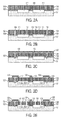
- Figs. 2A-2E are diagrams which illustrate a series of cross-sections illustrating processing steps to build the electric coupling from handle layer 101 to MEMS device layer 104 ready to bond to a base substrate 102 shown in Figure 1 .
- Fig. 2A is a diagram which illustrates the cross-section of an ESOI (engineered SOI) substrate with device layer 104 fusion-bonded to a handle silicon layer 101 with cavities 112.
- ESOI engineered SOI
- vias 106 are patterned on device layer 104 of ESOI substrate and etched through device layer 104, through thin dielectric layer 103, and into handle layer 101.
- vias 106 are patterned on device layer 104 of ESOI substrate and etched through device layer 104 and through thin dielectric layer 103 to expose a portion of the surface of handle layer 101.
- a conformal deposition of a conductive material 105 is then provided, as shown in Fig 2C , to fill via 106 to establish electrical coupling between device layer 104 and handle layer 101.
- a germanium layer 109 is then deposited onto the conductive material 105.
- the next step shown in Fig. 2D is to pattern and etch conductive material 105 and germanium layer 109 to form standoffs 121 from the conductive material 105, followed by MEMS device layer 104 pattern and etch, as shown in Fig. 2E to complete the MEMS substrate processing, ready to bond to a base substrate.
- the standoff 121 can be formed from both the conductive material 105 and a portion of the device layer 104 by partially etching into the device layer during standoff formation.
- Fig. 3 is a diagram which illustrates a cross-section of the bonded MEMS-base substrate device with an internal direct electric coupling in accordance with a second embodiment.
- the electric coupling path is formed from handle layer 201 to MEMS device layer 204, across dielectric film 203, and eventually to base substrate Al pad 207 after MEMS to base substrate AlGe eutectic bonding.
- An ESOI substrate 220 is comprised of a handle layer 201 with cavities 212 and a device layer 204, fusion bonded together with a thin dielectric layer 203 (such as silicon oxide) in between the device layer 204 and handle layer 201.
- the ESOI substrate is completed after device layer thinning.
- An electrical connection between handle layer 201 and device layer 204 can be achieved by etching at least one via 206 at any locations through device layer 204 and thin dielectric layer 203 into or exposing the surface of handle layer 201 and filling the via 206 by conductive materials, such as polysilicon, tungsten, titanium, titanium nitride, aluminum or germanium.
- the remaining conductive materials on device layer 204 could be removed by thinning, polishing or etching-back to expose device layer for standoff formation 205. Steps of germanium deposition, standoff pattern, germanium etch, device layer 204 pattern, and etch, will be processed to complete the MEMS substrate.
- the MEMS-base substrate integration is achieved by eutectic bonding of MEMS substrate with germanium pads 209 to base substrate with aluminum pads 207, where the AlGe bonding provides direct electrical coupling between MEMS substrate (handle 201 and device 204) and base substrate 202.
- the standoff 205 forms a ring around the MEMS structure
- the AlGe bond provides a hermetic seal for the MEMS structure.
- Via 206 can be positioned within or outside the seal ring formed by the standoff 205.
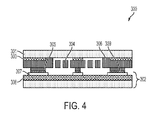
- Fig. 4 is a diagram illustrating a third embodiment of the electric coupling between handle layer 301, MEMS device layer 304, and base substrate 302 using polysilicon for the device layer 304 and AlGe eutectic bonding.
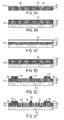
- the process flow and fabrication method of MEMS substrate using a surface micro-machining process technique are illustrated in Figs. 5A-5F.
- Figs. 5A-5F are diagrams which illustrate a series of cross-sections illustrating processing steps to build the electric coupling from handle layer 301 to device layer 306 ready to bond to a base substrate 302 for the device of Fig. 4 .
- a thin dielectric layer 303 typically silicon oxide
- a silicon layer 306 ( Fig. 5B ) is deposited onto the handle layer 301 followed by thinning and planarization, (for example grinding or chemical mechanical polishing) to desired device layer thickness.
- Fig. 5C illustrates an embodiment with a second thicker silicon device layer.
- an additional silicon wafer 311 can be bonded to the thin polysilicon 312 and thinned down to desired device thickness. The bonding of the additional silicon wafer 311 overcomes thickness limitations from conventional deposition techniques.
- Fig. 5E is a diagram which illustrates standoff 305 formation by patterning and etching into device layer 306.
- Fig. 5F is a diagram which illustrates patterning and etching silicon layer 306 to form MEMS structure 304.
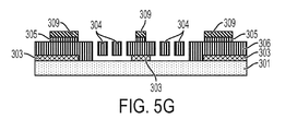
- the patterning and etching step is followed by etching the silicon oxide to release the device layer 304 as shown in Fig. 5G .
- the MEMS substrate is now ready to be integrated with a base substrate.
- the MEMS-base substrate integration is achieved by eutectic bonding of MEMS substrate with germanium pads 309 to base substrate with aluminum pads 307, where the AlGe bonding provides direct electrical coupling between MEMS substrate (handle 301 and device 305) and base substrate 302.
- AlGe bonding provides hermetic vacuum seal of the MEMS device.
Landscapes
- Engineering & Computer Science (AREA)
- Microelectronics & Electronic Packaging (AREA)
- Manufacturing & Machinery (AREA)
- Computer Hardware Design (AREA)
- Physics & Mathematics (AREA)
- Electromagnetism (AREA)
- Micromachines (AREA)
Applications Claiming Priority (1)
| Application Number | Priority Date | Filing Date | Title |
|---|---|---|---|
| US13/754,462 US8564076B1 (en) | 2013-01-30 | 2013-01-30 | Internal electrical contact for enclosed MEMS devices |
Publications (2)
| Publication Number | Publication Date |
|---|---|
| EP2762441A2 true EP2762441A2 (de) | 2014-08-06 |
| EP2762441A3 EP2762441A3 (de) | 2014-10-01 |
Family
ID=49355229
Family Applications (1)
| Application Number | Title | Priority Date | Filing Date |
|---|---|---|---|
| EP14153050.1A Withdrawn EP2762441A3 (de) | 2013-01-30 | 2014-01-29 | Interner elektrischer Kontakt für verkapselte MEMS-Vorrichtungen |
Country Status (4)
| Country | Link |
|---|---|
| US (4) | US8564076B1 (de) |
| EP (1) | EP2762441A3 (de) |
| CN (1) | CN103964366B (de) |
| TW (1) | TWI611531B (de) |
Families Citing this family (41)
| Publication number | Priority date | Publication date | Assignee | Title |
|---|---|---|---|---|
| US9452920B2 (en) * | 2013-01-30 | 2016-09-27 | Invensense, Inc. | Microelectromechanical system device with internal direct electric coupling |
| US8564076B1 (en) * | 2013-01-30 | 2013-10-22 | Invensense, Inc. | Internal electrical contact for enclosed MEMS devices |
| US9533873B2 (en) | 2013-02-05 | 2017-01-03 | Butterfly Network, Inc. | CMOS ultrasonic transducers and related apparatus and methods |
| US8916943B2 (en) * | 2013-03-01 | 2014-12-23 | Taiwan Semiconductor Manufacturing Company, Ltd. | MEMS devices having a plurality of cavities |
| WO2014151525A2 (en) | 2013-03-15 | 2014-09-25 | Butterfly Network, Inc. | Complementary metal oxide semiconductor (cmos) ultrasonic transducers and methods for forming the same |
| US10273147B2 (en) | 2013-07-08 | 2019-04-30 | Motion Engine Inc. | MEMS components and method of wafer-level manufacturing thereof |
| JP6339669B2 (ja) | 2013-07-08 | 2018-06-06 | モーション・エンジン・インコーポレーテッド | Memsデバイスおよび製造する方法 |
| WO2015013827A1 (en) | 2013-08-02 | 2015-02-05 | Motion Engine Inc. | Mems motion sensor for sub-resonance angular rate sensing |
| US9738511B2 (en) | 2013-09-13 | 2017-08-22 | Invensense, Inc. | Reduction of chipping damage to MEMS structure |
| WO2015103688A1 (en) | 2014-01-09 | 2015-07-16 | Motion Engine Inc. | Integrated mems system |
| US20150262902A1 (en) | 2014-03-12 | 2015-09-17 | Invensas Corporation | Integrated circuits protected by substrates with cavities, and methods of manufacture |
| US20170030788A1 (en) | 2014-04-10 | 2017-02-02 | Motion Engine Inc. | Mems pressure sensor |
| US9761557B2 (en) | 2014-04-28 | 2017-09-12 | Invensense, Inc. | CMOS-MEMS integration by sequential bonding method |
| US11674803B2 (en) | 2014-06-02 | 2023-06-13 | Motion Engine, Inc. | Multi-mass MEMS motion sensor |
| US9067779B1 (en) * | 2014-07-14 | 2015-06-30 | Butterfly Network, Inc. | Microfabricated ultrasonic transducers and related apparatus and methods |
| US20160090300A1 (en) * | 2014-09-30 | 2016-03-31 | Invensense, Inc. | Piezoelectric microphone with integrated cmos |
| US11287486B2 (en) | 2014-12-09 | 2022-03-29 | Motion Engine, Inc. | 3D MEMS magnetometer and associated methods |
| US10407299B2 (en) | 2015-01-15 | 2019-09-10 | Motion Engine Inc. | 3D MEMS device with hermetic cavity |
| KR101688724B1 (ko) | 2015-04-08 | 2016-12-21 | 주식회사 스탠딩에그 | Mems 장치 제조 방법 |
| US9718680B2 (en) * | 2015-06-12 | 2017-08-01 | Invensense, Inc. | CMOS-MEMS integrated device including a contact layer and methods of manufacture |
| US9809450B2 (en) * | 2015-08-27 | 2017-11-07 | Invensense, Inc. | CMOS-MEMS integration using metal silicide formation |
| US10155656B2 (en) * | 2015-10-19 | 2018-12-18 | Taiwan Semiconductor Manufacturing Co., Ltd. | Inter-poly connection for parasitic capacitor and die size improvement |
| DE102016100269B4 (de) | 2015-10-19 | 2020-01-16 | Taiwan Semiconductor Manufacturing Company, Ltd. | MEMS-Package mit Polysilicium-Zwischenlagenverbindung und zugehöriges Herstellungsverfahren |
| US10087072B2 (en) | 2016-05-04 | 2018-10-02 | United Microelectronics Corp. | Microelectromechanical system structure including thermal stability layer whose material has higher growth temperature, and method for fabricating the same |
| US9896327B2 (en) * | 2016-05-19 | 2018-02-20 | Invensense, Inc. | CMOS-MEMS structures with out-of-plane MEMS sensing gap |
| US9919915B2 (en) * | 2016-06-14 | 2018-03-20 | Invensense, Inc. | Method and system for MEMS devices with dual damascene formed electrodes |
| US10473920B2 (en) * | 2016-08-24 | 2019-11-12 | Stmicroelectronics S.R.L. | Hermetically sealed MEMS mirror and method of manufacture |
| US10002844B1 (en) | 2016-12-21 | 2018-06-19 | Invensas Bonding Technologies, Inc. | Bonded structures |
| US10567868B2 (en) * | 2017-01-26 | 2020-02-18 | AAC Technologies Pte. Ltd. | Sound generator |
| EP4220917A1 (de) * | 2017-03-13 | 2023-08-02 | Pioneer Corporation | Antriebsvorrichtung und abstandsmessvorrichtung |
| US10508030B2 (en) | 2017-03-21 | 2019-12-17 | Invensas Bonding Technologies, Inc. | Seal for microelectronic assembly |
| EP3642611B1 (de) | 2017-06-21 | 2024-02-14 | Butterfly Network, Inc. | Mikrogefertigter ultraschallwandler mit einzelnen zellen mit elektrisch isolierten elektrodenabschnitten |
| US10505006B2 (en) * | 2017-07-28 | 2019-12-10 | Invensense, Inc. | Proof mass and polysilicon electrode integrated thereon |
| US11380597B2 (en) | 2017-12-22 | 2022-07-05 | Invensas Bonding Technologies, Inc. | Bonded structures |
| US10923408B2 (en) | 2017-12-22 | 2021-02-16 | Invensas Bonding Technologies, Inc. | Cavity packages |
| CN108203076B (zh) * | 2018-01-03 | 2020-04-14 | 上海华虹宏力半导体制造有限公司 | 晶圆键合方法 |
| US11004757B2 (en) | 2018-05-14 | 2021-05-11 | Invensas Bonding Technologies, Inc. | Bonded structures |
| CN111377395B (zh) * | 2018-12-27 | 2023-09-08 | 中芯集成电路(宁波)有限公司上海分公司 | Mems封装结构及其制作方法 |
| US12374641B2 (en) | 2019-06-12 | 2025-07-29 | Adeia Semiconductor Bonding Technologies Inc. | Sealed bonded structures and methods for forming the same |
| CN114620671B (zh) * | 2022-05-16 | 2022-08-30 | 苏州敏芯微电子技术股份有限公司 | 一种微机电系统传感器及其制备方法 |
| CN114789987B (zh) * | 2022-06-23 | 2022-09-27 | 苏州敏芯微电子技术股份有限公司 | 用于感测的封装结构及其制作方法 |
Family Cites Families (30)
| Publication number | Priority date | Publication date | Assignee | Title |
|---|---|---|---|---|
| US6586841B1 (en) * | 2000-02-23 | 2003-07-01 | Onix Microsystems, Inc. | Mechanical landing pad formed on the underside of a MEMS device |
| US6835589B2 (en) | 2002-11-14 | 2004-12-28 | International Business Machines Corporation | Three-dimensional integrated CMOS-MEMS device and process for making the same |
| US7291513B2 (en) | 2003-12-15 | 2007-11-06 | Dalsa Semiconductor Inc. | Hermetic wafer-level packaging for MEMS devices with low-temperature metallurgy |
| US6936918B2 (en) * | 2003-12-15 | 2005-08-30 | Analog Devices, Inc. | MEMS device with conductive path through substrate |
| US20060163698A1 (en) | 2005-01-25 | 2006-07-27 | Sony Corporation | Method and apparatus for wafer to wafer bonding |
| US7442570B2 (en) | 2005-03-18 | 2008-10-28 | Invensence Inc. | Method of fabrication of a AL/GE bonding in a wafer packaging environment and a product produced therefrom |
| DE102005015584B4 (de) * | 2005-04-05 | 2010-09-02 | Litef Gmbh | Verfahren zur Herstellung eines mikromechanischen Bauteils |
| FI119728B (fi) * | 2005-11-23 | 2009-02-27 | Vti Technologies Oy | Menetelmä mikroelektromekaanisen komponentin valmistamiseksi ja mikroelektromekaaninen komponentti |
| US7675162B2 (en) * | 2006-10-03 | 2010-03-09 | Innovative Micro Technology | Interconnect structure using through wafer vias and method of fabrication |
| KR100833508B1 (ko) * | 2006-12-07 | 2008-05-29 | 한국전자통신연구원 | 멤즈 패키지 및 그 방법 |
| US8264307B2 (en) * | 2007-05-09 | 2012-09-11 | Innovative Micro Technology | Dual substrate MEMS plate switch and method of manufacture |
| JP4766143B2 (ja) * | 2008-09-15 | 2011-09-07 | 株式会社デンソー | 半導体装置およびその製造方法 |
| US8119498B2 (en) | 2008-09-24 | 2012-02-21 | Evigia Systems, Inc. | Wafer bonding method and wafer stack formed thereby |
| US8299506B2 (en) | 2008-12-01 | 2012-10-30 | Honeywell International Inc. | Integration of MEMS and CMOS devices on a chip |
| US8012785B2 (en) | 2009-04-24 | 2011-09-06 | Taiwan Semiconductor Manufacturing Company, Ltd. | Method of fabricating an integrated CMOS-MEMS device |
| US8093119B2 (en) | 2009-06-24 | 2012-01-10 | Solid State System Co., Ltd. | CMOS microelectromechanical system (MEMS) device and fabrication method thereof |
| TW201103107A (en) * | 2009-07-07 | 2011-01-16 | Jung-Tang Huang | Method for packaging micromachined devices |
| US8513041B2 (en) | 2009-11-30 | 2013-08-20 | Pixart Imaging Corporation | MEMS integrated chip and method for making same |
| US8217474B2 (en) | 2009-12-28 | 2012-07-10 | Solid State System Co., Ltd. | Hermetic MEMS device and method for fabricating hermetic MEMS device and package structure of MEMS device |
| US8584522B2 (en) * | 2010-04-30 | 2013-11-19 | Qualcomm Mems Technologies, Inc. | Micromachined piezoelectric x-axis gyroscope |
| TWI434803B (zh) * | 2010-06-30 | 2014-04-21 | 財團法人工業技術研究院 | 微機電元件與電路晶片之整合裝置及其製造方法 |
| US8648468B2 (en) | 2010-07-29 | 2014-02-11 | Taiwan Semiconductor Manufacturing Company, Ltd. | Hermetic wafer level packaging |
| US8507358B2 (en) | 2010-08-27 | 2013-08-13 | Taiwan Semiconductor Manufacturing Company, Ltd. | Composite wafer semiconductor |
| US8810027B2 (en) | 2010-09-27 | 2014-08-19 | Taiwan Semiconductor Manufacturing Company, Ltd. | Bond ring for a first and second substrate |
| US8674495B2 (en) * | 2010-10-08 | 2014-03-18 | Taiwan Semiconductor Manufacturing Company, Ltd. | Package systems having a eutectic bonding material and manufacturing methods thereof |
| US9000578B2 (en) * | 2010-10-08 | 2015-04-07 | Taiwan Semiconductor Manufacturing Company, Ltd. | Package systems having an opening in a substrate thereof and manufacturing methods thereof |
| FR2977885A1 (fr) * | 2011-07-12 | 2013-01-18 | Commissariat Energie Atomique | Procede de realisation d'une structure a electrode enterree par report direct et structure ainsi obtenue |
| US9365416B2 (en) * | 2011-08-15 | 2016-06-14 | Taiwan Semiconductor Manufacturing Company, Ltd. | Structure and method for motion sensor |
| CN102798489B (zh) * | 2011-10-21 | 2015-04-15 | 清华大学 | 一种压力传感器及其制备方法 |
| US8564076B1 (en) * | 2013-01-30 | 2013-10-22 | Invensense, Inc. | Internal electrical contact for enclosed MEMS devices |
-
2013
- 2013-01-30 US US13/754,462 patent/US8564076B1/en active Active
- 2013-09-20 US US14/033,366 patent/US8822252B2/en active Active
-
2014
- 2014-01-28 TW TW103103179A patent/TWI611531B/zh active
- 2014-01-29 EP EP14153050.1A patent/EP2762441A3/de not_active Withdrawn
- 2014-01-30 CN CN201410044191.1A patent/CN103964366B/zh active Active
- 2014-08-11 US US14/456,973 patent/US8945969B2/en active Active
-
2015
- 2015-01-06 US US14/590,839 patent/US9221676B2/en active Active
Non-Patent Citations (1)
| Title |
|---|
| None |
Also Published As
| Publication number | Publication date |
|---|---|
| US20150336792A1 (en) | 2015-11-26 |
| US8822252B2 (en) | 2014-09-02 |
| TWI611531B (zh) | 2018-01-11 |
| US9221676B2 (en) | 2015-12-29 |
| US8945969B2 (en) | 2015-02-03 |
| US8564076B1 (en) | 2013-10-22 |
| TW201442173A (zh) | 2014-11-01 |
| CN103964366A (zh) | 2014-08-06 |
| EP2762441A3 (de) | 2014-10-01 |
| US20140349434A1 (en) | 2014-11-27 |
| CN103964366B (zh) | 2017-09-12 |
| US20140213007A1 (en) | 2014-07-31 |
Similar Documents
| Publication | Publication Date | Title |
|---|---|---|
| US9221676B2 (en) | Internal electrical contact for enclosed MEMS devices | |
| US9452920B2 (en) | Microelectromechanical system device with internal direct electric coupling | |
| US9738512B2 (en) | CMOS-MEMS integrated device including multiple cavities at different controlled pressures and methods of manufacture | |
| US10486964B2 (en) | Method for forming a micro-electro mechanical system (MEMS) including bonding a MEMS substrate to a CMOS substrate via a blocking layer | |
| US10155659B2 (en) | Vacuum sealed MEMS and CMOS package | |
| US9085455B2 (en) | MEMS devices and methods for forming same | |
| TWI503953B (zh) | 半導體裝置及其製造方法 | |
| US20200131028A1 (en) | Cmos-mems integration with through-chip via process | |
| US11097942B2 (en) | Through silicon via (TSV) formation in integrated circuits | |
| EP2778118B1 (de) | Integrierte Struktur mit bidirectionalem vertikalem Antrieb | |
| CN107697882B (zh) | 用于制造半导体器件的工艺以及相应半导体器件 | |
| TWI691455B (zh) | 包含接觸層的互補式金屬氧化半導體-微電子機械系統(cmos-mems)積體裝置和製造方法 | |
| EP2848586A1 (de) | Waferebenenverkapselungsstruktur und deren Herstellungsverfahren | |
| US10882737B2 (en) | Through silicon interposer wafer and method of manufacturing the same | |
| US20070298532A1 (en) | Micro-Electro-mechanical (MEMS) encapsulation using buried porous silicon |
Legal Events
| Date | Code | Title | Description |
|---|---|---|---|
| PUAI | Public reference made under article 153(3) epc to a published international application that has entered the european phase |
Free format text: ORIGINAL CODE: 0009012 |
|
| 17P | Request for examination filed |
Effective date: 20140129 |
|
| AK | Designated contracting states |
Kind code of ref document: A2 Designated state(s): AL AT BE BG CH CY CZ DE DK EE ES FI FR GB GR HR HU IE IS IT LI LT LU LV MC MK MT NL NO PL PT RO RS SE SI SK SM TR |
|
| AX | Request for extension of the european patent |
Extension state: BA ME |
|
| PUAL | Search report despatched |
Free format text: ORIGINAL CODE: 0009013 |
|
| AK | Designated contracting states |
Kind code of ref document: A3 Designated state(s): AL AT BE BG CH CY CZ DE DK EE ES FI FR GB GR HR HU IE IS IT LI LT LU LV MC MK MT NL NO PL PT RO RS SE SI SK SM TR |
|
| AX | Request for extension of the european patent |
Extension state: BA ME |
|
| RIC1 | Information provided on ipc code assigned before grant |
Ipc: B81B 7/00 20060101AFI20140828BHEP |
|
| R17P | Request for examination filed (corrected) |
Effective date: 20150401 |
|
| RBV | Designated contracting states (corrected) |
Designated state(s): AL AT BE BG CH CY CZ DE DK EE ES FI FR GB GR HR HU IE IS IT LI LT LU LV MC MK MT NL NO PL PT RO RS SE SI SK SM TR |
|
| 17Q | First examination report despatched |
Effective date: 20171113 |
|
| STAA | Information on the status of an ep patent application or granted ep patent |
Free format text: STATUS: THE APPLICATION IS DEEMED TO BE WITHDRAWN |
|
| 18D | Application deemed to be withdrawn |
Effective date: 20181204 |