EP2760791B1 - Reactor and method for production of silicon by chemical vapor deposition - Google Patents
Reactor and method for production of silicon by chemical vapor deposition Download PDFInfo
- Publication number
- EP2760791B1 EP2760791B1 EP12835547.6A EP12835547A EP2760791B1 EP 2760791 B1 EP2760791 B1 EP 2760791B1 EP 12835547 A EP12835547 A EP 12835547A EP 2760791 B1 EP2760791 B1 EP 2760791B1
- Authority
- EP
- European Patent Office
- Prior art keywords
- reactor
- silicon
- particles
- vapour deposition
- chemical vapour
- Prior art date
- Legal status (The legal status is an assumption and is not a legal conclusion. Google has not performed a legal analysis and makes no representation as to the accuracy of the status listed.)
- Active
Links
- 229910052710 silicon Inorganic materials 0.000 title claims description 95
- 239000010703 silicon Substances 0.000 title claims description 95
- 238000005229 chemical vapour deposition Methods 0.000 title claims description 48
- 238000004519 manufacturing process Methods 0.000 title claims description 28
- 239000002245 particle Substances 0.000 claims description 117
- XUIMIQQOPSSXEZ-UHFFFAOYSA-N Silicon Chemical compound [Si] XUIMIQQOPSSXEZ-UHFFFAOYSA-N 0.000 claims description 112
- 238000000034 method Methods 0.000 claims description 22
- 239000012495 reaction gas Substances 0.000 claims description 22
- 239000007787 solid Substances 0.000 claims description 21
- 239000007789 gas Substances 0.000 claims description 18
- 239000000463 material Substances 0.000 claims description 18
- 239000011863 silicon-based powder Substances 0.000 claims description 12
- BLRPTPMANUNPDV-UHFFFAOYSA-N Silane Chemical compound [SiH4] BLRPTPMANUNPDV-UHFFFAOYSA-N 0.000 claims description 6
- 229910000077 silane Inorganic materials 0.000 claims description 6
- 230000015572 biosynthetic process Effects 0.000 claims description 4
- 238000002360 preparation method Methods 0.000 claims description 2
- 230000008569 process Effects 0.000 description 9
- 239000004576 sand Substances 0.000 description 7
- 230000001133 acceleration Effects 0.000 description 5
- 238000000151 deposition Methods 0.000 description 5
- 230000008901 benefit Effects 0.000 description 4
- 229910021419 crystalline silicon Inorganic materials 0.000 description 4
- 230000008021 deposition Effects 0.000 description 4
- 239000000428 dust Substances 0.000 description 4
- 238000011109 contamination Methods 0.000 description 3
- 238000000354 decomposition reaction Methods 0.000 description 3
- 230000005484 gravity Effects 0.000 description 3
- 238000010438 heat treatment Methods 0.000 description 3
- 229910021420 polycrystalline silicon Inorganic materials 0.000 description 3
- 238000000926 separation method Methods 0.000 description 3
- XKRFYHLGVUSROY-UHFFFAOYSA-N Argon Chemical compound [Ar] XKRFYHLGVUSROY-UHFFFAOYSA-N 0.000 description 2
- NHWNVPNZGGXQQV-UHFFFAOYSA-J [Si+4].[O-]N=O.[O-]N=O.[O-]N=O.[O-]N=O Chemical compound [Si+4].[O-]N=O.[O-]N=O.[O-]N=O.[O-]N=O NHWNVPNZGGXQQV-UHFFFAOYSA-J 0.000 description 2
- 229910021417 amorphous silicon Inorganic materials 0.000 description 2
- -1 hydrogen and argon Chemical compound 0.000 description 2
- 230000006872 improvement Effects 0.000 description 2
- 239000000843 powder Substances 0.000 description 2
- 239000010453 quartz Substances 0.000 description 2
- VYPSYNLAJGMNEJ-UHFFFAOYSA-N silicon dioxide Inorganic materials O=[Si]=O VYPSYNLAJGMNEJ-UHFFFAOYSA-N 0.000 description 2
- UFHFLCQGNIYNRP-UHFFFAOYSA-N Hydrogen Chemical compound [H][H] UFHFLCQGNIYNRP-UHFFFAOYSA-N 0.000 description 1
- 229910052786 argon Inorganic materials 0.000 description 1
- 230000004888 barrier function Effects 0.000 description 1
- 238000006243 chemical reaction Methods 0.000 description 1
- 239000011362 coarse particle Substances 0.000 description 1
- 239000011248 coating agent Substances 0.000 description 1
- 238000000576 coating method Methods 0.000 description 1
- 238000001816 cooling Methods 0.000 description 1
- 238000009792 diffusion process Methods 0.000 description 1
- 230000000694 effects Effects 0.000 description 1
- 238000005265 energy consumption Methods 0.000 description 1
- 230000002349 favourable effect Effects 0.000 description 1
- 239000012634 fragment Substances 0.000 description 1
- 239000001257 hydrogen Substances 0.000 description 1
- 229910052739 hydrogen Inorganic materials 0.000 description 1
- 239000011261 inert gas Substances 0.000 description 1
- 239000007788 liquid Substances 0.000 description 1
- 239000000203 mixture Substances 0.000 description 1
- 229910021421 monocrystalline silicon Inorganic materials 0.000 description 1
- 239000011236 particulate material Substances 0.000 description 1
- 238000012805 post-processing Methods 0.000 description 1
- 238000012545 processing Methods 0.000 description 1
- 239000002994 raw material Substances 0.000 description 1
- 238000005245 sintering Methods 0.000 description 1
- 239000007921 spray Substances 0.000 description 1
- ZDHXKXAHOVTTAH-UHFFFAOYSA-N trichlorosilane Chemical compound Cl[SiH](Cl)Cl ZDHXKXAHOVTTAH-UHFFFAOYSA-N 0.000 description 1
- 239000005052 trichlorosilane Substances 0.000 description 1
Images

Classifications
-
- H—ELECTRICITY
- H01—ELECTRIC ELEMENTS
- H01L—SEMICONDUCTOR DEVICES NOT COVERED BY CLASS H10
- H01L21/00—Processes or apparatus adapted for the manufacture or treatment of semiconductor or solid state devices or of parts thereof
- H01L21/02—Manufacture or treatment of semiconductor devices or of parts thereof
- H01L21/02104—Forming layers
- H01L21/02365—Forming inorganic semiconducting materials on a substrate
- H01L21/02612—Formation types
- H01L21/02617—Deposition types
- H01L21/0262—Reduction or decomposition of gaseous compounds, e.g. CVD
-
- C—CHEMISTRY; METALLURGY
- C01—INORGANIC CHEMISTRY
- C01B—NON-METALLIC ELEMENTS; COMPOUNDS THEREOF; METALLOIDS OR COMPOUNDS THEREOF NOT COVERED BY SUBCLASS C01C
- C01B33/00—Silicon; Compounds thereof
- C01B33/02—Silicon
- C01B33/021—Preparation
- C01B33/027—Preparation by decomposition or reduction of gaseous or vaporised silicon compounds other than silica or silica-containing material
-
- H—ELECTRICITY
- H01—ELECTRIC ELEMENTS
- H01L—SEMICONDUCTOR DEVICES NOT COVERED BY CLASS H10
- H01L21/00—Processes or apparatus adapted for the manufacture or treatment of semiconductor or solid state devices or of parts thereof
- H01L21/02—Manufacture or treatment of semiconductor devices or of parts thereof
- H01L21/02104—Forming layers
- H01L21/02365—Forming inorganic semiconducting materials on a substrate
- H01L21/02518—Deposited layers
- H01L21/02521—Materials
- H01L21/02524—Group 14 semiconducting materials
- H01L21/02532—Silicon, silicon germanium, germanium
Definitions
- the present invention relates to the manufacture of silicon for application in sun cells and electronics.
- the invention relates to a reactor and a method for production of silicon, in particular the deposition surface of a rotating reactor for manufacture of silicon by chemical vapour deposition, CVD.
- Silicon is a critical raw material for both the electronics industry and the solar cell industry. Although there are alternative materials for specific applications, multi-crystalline and mono-crystalline silicon will be the material of choice for the foreseeable future. Improved availability and economics of production of multi-crystalline silicon will increase the growth possibilities for both these industries, in particular the application of solar cells for renewable energy.
- CVD uses a fluidized bed, whereby silicon seed particles are fluidised and held in an upward flowing gas stream, with the gas stream comprising silicon-containing gas from which silicon can be deposited onto the seed particles.
- US 2008/213156 A1 discloses a reactor for silicon production by gas decomposition comprising coating of the reactor wall with a separation layer which is especially of silicon powder.
- WO 2010/136529 A1 discloses a reactor for producing silicon by chemical vapor deposition comprising a reactor body forming container, inlet for silicon-bearing gas, outlet and heating device, where main part of reactor is produced from silicon.
- a rotating CVD reactor has been developed and a patent has been applied for by Dynatec Engineering with the patent applications NO 2009 2111 and NO 2010 0210 .
- a reactor for the manufacture of silicon by chemical vapour deposition is thus provided, with the reactor comprising a reactor body that forms a container, with at least one inlet for a silicon-containing gas, at least one outlet and at least one heat appliance as a part of, or operatively arranged to, the reactor.
- the reactor is characterised in that it rotates so that the reaction gas is subjected to centripetal acceleration.
- such a reactor is designated as a Dynatec reactor.
- the principle for a Dynatec reactor is that a silicon-containing gas, preferably silane, is fed into a rotating, heated container.
- the difference in density between the reaction gas and the residual gas makes it possible to separate the gases with the help of the centripetal acceleration.
- the heavy reaction gas is forced out from the centre of the container, whereupon it decomposes when it is heated up by the inner wall of the container, whereupon silicon is deposited.
- the invention provides a reactor for the manufacture of solid silicon by chemical vapour deposition (CVD), the reactor comprises a reactor body that can rotate around an axis with the help of a rotation device operatively arranged to the reactor, at least one sidewall that surrounds the reactor body, at least one inlet for reaction gas, at least one outlet for residual gas and at least one heat appliance operatively arranged to the reactor.
- the reactor is distinguished in that during operation for the manufacture of solid silicon by CVD, the reactor comprises a loose layer of particles on the inside of, at least, one heated side wall, the loose layer of particles is held in place by rotation of the reactor during operation and the solid silicon is deposited on the loose layer of particles.
- the reactor rotates during operation and the layer of particles comprises loose particles, at least nearest the reactor body. It is most preferred that the whole, or part of, the particle layer, in particular nearest the reactor body, comprises loose particles.
- solid silicon is chemically vapour deposited on the layer of particles during operation, with the sidewall with the layer of particles being held at CVD conditions, and it is thereby easier to take out the solid silicon.
- Loose particles in the layer are held in place by the rotation of the reactor or more particularly, by the centripetal forces.
- a layer comprising loose particles against the reactor body and the deposited solid silicon ensures a simple removal of the produced silicon.
- the outer part of the layer can comprise a layer of bound particles.
- the Dynatec reactor With the Dynatec reactor, if the reactor shall be re-used, it can be a challenge to remove the completed block of silicon from the reactor after so much silicon has been deposited inside the reactor that it is not appropriate to continue the process for the manufacture of silicon. The block of deposited silicon must then be removed before the process can be started up again.
- the silicon With the present invention the silicon will come off the inner wall of the reactor easily because the layer of particles functions as a ball-bearing layer or a gliding layer from where the block of silicon can be taken out more easily. Thereby, the advantage is that the production process can be operated much more continuously, which reduces the production costs.
- the reactor can comprise a pipe section or be assembled by several sidewalls or sections, preferably so that the reactor can be opened easily or the block of silicon can be extruded out.
- the cross section of the reactor body orthogonally to the axis is preferably circular, but not necessarily, however it is preferably circular, with the layer of particles on the sidewall in an operation mode, with rotation and heating for the manufacture of silicon by CVD, to achieve the optimal operating conditions.
- particles are fed in or material is arranged in the reactor so that the centripetal acceleration arranges the particle layer so that a circular cross section is achieved.
- layer of particles one means the material which is, or during the operating conditions becomes, particulate so that the produced block of silicon can be taken out of the reactor easily.
- the material can be fed in as a solid, a liquid or a semiliquid.
- the term layer of particles also comprises deposits or material which during heating and rotation of the reactor intentionally break up to particulate material, shell fragments, fibres or other forms that give the intended gliding effect which makes taking out the produced blocks of silicon simpler.
- the reactor does not necessarily have to have a top and a bottom, as one of or both the top and bottom can be external parts, for example, a rotation table and a top that can be folded in a rotation appliance and which rotates in the same direction.
- a rotation table and a top that can be folded in a rotation appliance and which rotates in the same direction.
- the layer of particles preferably comprises material which contaminates the produced silicon to the smallest extent possible, it is preferred that the particles of silicon are of a metallurgical quality or purer, most preferred is silicon of the same purity as the silicon that is chemically vapour deposited. It is an advantage that the layer of particles comprises, at least over a part of the thickness, for example, over the thickness of at least three median particle diameters of, in the main, round particles, thereby to achieve a good ball-bearing functionality.
- the reactor is preferably formed as a pipe section that can rotate about its own axis. Thereby, the reactor can have any orientation during operation, which can be very practical.
- the reactor is formed as a standing, conical pipe section that can rotate around its longitudinal axis, with a circular inner cross section and the largest diameter at the upper end.
- the sidewall of the reactor has a taper that can be adapted so that the particle layer lies naturally correct onto the inner sidewall of the reactor.
- the force of gravity is balanced on the particles against the vertical component in the counter force from the wall.
- a typical reactor with a 2-pole electro motor driven at 50 Hz with 3000 rotations per minute, rpm, will generate a centripetal acceleration of 1000 g on the particles, thus the centripetal acceleration is 1000 times the force of gravity.
- a balancing vertical component in the counter force is only 1/1000 and the taper can be found directly by finding the arctan of 1/1000. This is also the case for other speeds of rotation and different inner reactor diameters, as the angle can be adjusted so that the force of gravity and the vertical component of the counter force from the wall on the particles are balanced against each other.
- the reactor is formed with an outer layer of particles that is fastened to the sidewall of the reactor, for example, by sintering or fusing.
- the outer particle layer means longer from the centre axis than the inner particle layer, i.e. innermost against the reactor wall. Thereby it is not only simpler to get a particle layer but it will be simpler to get a layer of coarser particles outermost, nearest the wall and finer particles with a larger surface area innermost against the reactor body. Thereby, the particles will not so easily go through a separation over time so that it can be easier to achieve a layer with fine, non-contaminated particles with a large surface area innermost against the reactor body. Natural radial separation can otherwise lead to that coarse particles lie innermost and fine outermost against the wall of the reactor.
- the reactor preferably comprises one outlet and at least one inlet at the same end, the inlet or the inlets are arranged concentrically outside the outlet.
- one end can be without perforations for simple placing on a rotating base and spent reaction gas, or residual gas or inert gas that can, for example, have a density 1/16 of the density of rich reaction gas, will be taken out at the centre line where it will collect naturally, while rich reaction gas will be fed in nearer the sidewall where it collects naturally. In this way the flow pattern is improved.
- the inlet and the outlet can be at opposite ends so that the reactor is the through-flow reactor.
- One or more inlets can be arranged at the bottom and one or more outlets at the top, or vice versa.
- the reactor comprises several sub-volumes, for example, preferably cylindrical sub-volumes that sit fitted next to each other on, or along, a circle around the rotational axis of the reactor.
- This is an embodiment that has been tested and it had the advantage of having less turbulence inside the reactor and simpler feeding out of smaller blocks of silicon after completion of the process.
- the reactor preferably comprises a particle layer of silicon powder formed by operation of the reactor containing reaction gas for chemical vapour deposition before the start-up of chemical vapour deposition for the production of solid silicon as will be explained in detail below.
- the invention also provides a method for the manufacture of solid silicon by chemical vapour deposition (CVD), preferably by the use of the reactor according to the invention.
- the method is distinguished producing a particle layer from the reaction gas in the reactor or importing particles for the formation of an inner loose particle layer which is held in place by rotation of the reactor during operation on the heated inner wall surface of the reactor, importing reaction gas for chemical vapour deposition, producing solid silicon by chemical vapour deposition on the loose particle layer, loosening the produced silicon from the particle layer and taking it out and carrying out any preparation of the inner surface of the reactor before the production of the silicon is continued by repeating the steps of the method.
- CVD chemical vapour deposition
- the reactor is preferably kept warm when going through the steps of the method and in the rotation up to the step of the chemical vapour deposition, for efficient production.
- a particle layer of silicon powder can advantageously be formed by the operation of the reactor containing reaction gas for chemical vapour deposition, preferably silane, before the start-up of chemical vapour deposition for production of solid silicon, by controlling the concentration and pressure of the reaction gas and temperature and speed of rotation of the reactor, so that, in the main, only silicon powder (so-called "fines" of different types) amorphous and/or crystalline is produced.
- silane at atmospheric pressure
- the formation of amorphous silicon powder starts at a temperature of 420 °C, at ca. 600-610 °C crystalline silicon powder is formed.
- Previously formed amorphous silicon powder can be converted to crystalline silicon powder at the temperature where crystalline silicon powder is formed directly. Note that there can be parallel unwanted reactions, particularly at other temperatures than those mentioned and other pressures, and with other gases. Therefore, it must be tested if the conditions that have been mentioned should be adjusted if the reactor contains gases other than silane.
- the invention also provides use of a reactor according to the invention for the manufacture of silicon by chemical vapour deposition (CVD).
- CVD chemical vapour deposition
- the invention also provides use of a loose particle layer on the inner reactor wall in a reactor for chemical vapour deposition (CVD) of solid silicon, to simplify the removal of produced solid silicon from the reactor, the loose particle layer is kept in place by rotation of the reactor during operation.
- CVD chemical vapour deposition
- the particle layer can comprise small and/or large particles that are hollow, compact or porous or with varying porosity in the form of a dust, powder, sand, small balls or other small particles that are placed or settle as a thin layer on the inside of the reactor or the inner wall of the container. It is an advantage to place or spray a thin layer of powder, small balls or other small particles on the inside of the reactor wall.
- the centripetal forces that arise in the rotating reactor container will hold the particles in place on the wall at the same time as they will help to form a layer with a circular inner cross section.
- the particles are distributed evenly over the inner wall of the reactor cylinder by the centripetal force after the reactor has been made to rotate.
- the reactor according to the invention can comprise the features that are described here or illustrated in any operative combination, every such combination is an embodiment of the present invention.
- the method according to the invention can comprise features or steps that are described here or illustrated in any operative combination, every such combination is an embodiment of the present invention.
- the reactor rotates during operation with chemical vapour deposition of solid silicon, and preferably also during the formation of the particle layer of fine silicon powder.
- the reactor must, of course, be rotated during production such that the layer is held in place by the centripetal force.
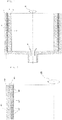
- the reactor comprises, in the main, a container (2), preferably formed as a cylinder with a circular, or approximately circular cross section, with an inlet for gas at the one end and an outlet at the other end or same end, and with the supply of heat on the outside and possibly on the inside too.
- the reactor is operatively arranged to an appliance to set the reactor in rotation (10), such as a motor.
- the particles (1) are distributed over the inner wall (4) of the reactor container (2) after it has been made to rotate (10) so that there will be an even layer of particles on the whole of the reactor wall (4). Thereby, the particles (1) will lie as a layer of particles (6) on the inside (4) of the reactor tube (2) and appear as an inner tube in the reactor container (2).
- the silicon deposits (3) will first be formed on the inside (5) of the particle layer (6).
- the particles (1) can be in the form of sand, dust or small balls in a hollow, porous or compact form, preferably of a material that leads to very little contamination.
- a material that leads to very little contamination examples of preferred materials are quartz and silicon nitrite, but most preferred will be particles of sand or dust of super pure crystalline silicon.
- the deposits (3) of silicon will start on the inside (5) of the particle layer (6) so that the particle layer (6) remains lying between the reactor wall (2) and the silicon deposits (3).
- the inside (5) of the particle layer (6) comes in direct contact with the silicon deposits (3) and it is therefore important that the particle layer (6) does not contaminate the silicon (3).
- the particle layer (6) of a non-contaminating material will act as a barrier against contamination from the reactor wall (2) and all other materials and matter lying outside.
- the particle layer (6) ensures that there is no direct contact between the silicon deposits (3) and the inside (4) of the reactor container (2) the large centripetal forces at the reactor wall (4) generated by the rotation (10) will work against diffusion of material in towards the silicon deposits (3). Therefore, a particle layer (6) with non-contaminating particles (1) on the inside (4) of the rotating (10) reactor container (2) will lead to very pure silicon deposits (3).
- the particle layer (6) should preferentially be put onto the inside (4) of the reactor container (2) after the reactor has started to rotate (10).
- the particles (1) can be sprayed onto the reactor wall (4) and the thickness and form can be adjusted afterwards by going down with a tool that touches the particle layer (6) according to the principle of a lathe.
- the centripetal force will ensure that the particles (1) remain on the reactor wall (4).
- the same force will also ensure that the particles (1) distribute themselves evenly over the reactor wall (4).
- the particles (1) can have different sizes and shapes, either as dust, sand or small balls.
- the particles can be put on in a tiered fashion (9), with x number of layers of particles of a similar or different material and/or sizes and shapes in every tier, preferably with particles (1) with a round ball shape or approximate round ball shape against the reactor wall (4) and smaller particles (1) against the silicon deposits (5).
- This will be preferred when a completed block of silicon shall be taken out of the reactor.
- the ball formed particles against the reactor wall (4) will function as a ball-bearing between the block of silicon (3) and the reactor wall (4).
- Another preferential putting on of the particle layer (6), illustrated in Figure 3 is to put on the particle layer at an angle (8) and/or on a slanting (7) reactor wall (4).
- the CVD process can start.
- a silicon-containing reaction gas (11) is fed into the reactor through an inlet at the one end of the reactor.
- the reaction gas (11) is forced outwards towards the particle layer (6) by the centripetal forces, where it is heated up to above the decomposition temperature.
- Super pure silicon (3) is then deposited on the inside (5) of the layer of particles so that the reactor body gradually becomes overgrown.
- the process is stopped when the reactor body is blocked by growth, or until there is no purpose in continuing to run the reactor any further.
- the supply of reaction gas (11) and the block of silicon (3) is taken out.
- a new particle layer (6) is put on and the process can start up again. With the use of silicon sand in the particle layer (6) nearest the silicon deposits (5) the need for processing of the finished block of silicon will be less.
Landscapes
- Engineering & Computer Science (AREA)
- Chemical & Material Sciences (AREA)
- Organic Chemistry (AREA)
- General Physics & Mathematics (AREA)
- Physics & Mathematics (AREA)
- Condensed Matter Physics & Semiconductors (AREA)
- Manufacturing & Machinery (AREA)
- Computer Hardware Design (AREA)
- Microelectronics & Electronic Packaging (AREA)
- Power Engineering (AREA)
- Inorganic Chemistry (AREA)
- Silicon Compounds (AREA)
- Chemical Vapour Deposition (AREA)
Description
- The present invention relates to the manufacture of silicon for application in sun cells and electronics. In more detail, the invention relates to a reactor and a method for production of silicon, in particular the deposition surface of a rotating reactor for manufacture of silicon by chemical vapour deposition, CVD.
- The development of new methods to use renewable, non-polluting energy sources is essential to meet future needs for energy. Energy from the sun is one of the energy sources which are of the greatest interest in this context.
- Silicon is a critical raw material for both the electronics industry and the solar cell industry. Although there are alternative materials for specific applications, multi-crystalline and mono-crystalline silicon will be the material of choice for the foreseeable future. Improved availability and economics of production of multi-crystalline silicon will increase the growth possibilities for both these industries, in particular the application of solar cells for renewable energy.
- Currently, to manufacture silicon of a satisfactory purity for use in solar cells or electronics, chemical vapour deposition methods (CVD - Chemical Vapour Deposition) are primarily used. Different embodiments of the Siemens process are the most used forms of CVD for the manufacture of polycrystalline silicon. In this method, silicon containing gases, such as silane or trichlorosilane, and other gases such as hydrogen and argon, are fed into a cooled container and silicon is deposited on one or more resistance-heated rods. The process is very energy and labour demanding. A more detailed description of the most used process can be found in the patent
US 3,979,490 . - Another CVD method uses a fluidized bed, whereby silicon seed particles are fluidised and held in an upward flowing gas stream, with the gas stream comprising silicon-containing gas from which silicon can be deposited onto the seed particles. A full description of CVD methods with a fluidised bed and associated equipment and operating parameters for the manufacture of silicon, including gas mixtures, temperatures for the deposition and related problems and limitations can be found in the patents
US 4,818,495 andUS 5,810 ,934 , and reference is given to these publications for more information. -
US 2008/213156 A1 discloses a reactor for silicon production by gas decomposition comprising coating of the reactor wall with a separation layer which is especially of silicon powder. -
WO 2010/136529 A1 discloses a reactor for producing silicon by chemical vapor deposition comprising a reactor body forming container, inlet for silicon-bearing gas, outlet and heating device, where main part of reactor is produced from silicon. A rotating CVD reactor has been developed and a patent has been applied for by Dynatec Engineering with the patent applicationsNO 2009 2111 NO 2010 0210 - The principle for a Dynatec reactor is that a silicon-containing gas, preferably silane, is fed into a rotating, heated container. The difference in density between the reaction gas and the residual gas makes it possible to separate the gases with the help of the centripetal acceleration. The heavy reaction gas is forced out from the centre of the container, whereupon it decomposes when it is heated up by the inner wall of the container, whereupon silicon is deposited. This gives a higher rate of deposition and a better utilisation of the reaction gas, at the same time as the need for selective cooling of surfaces where the decomposition shall not occur is minimised. Together, this reduces the energy consumption per kilo produced silicon. However, there is a need for further improvement of the Dynatec reactor to lower the cost per produced kg super-clean silicon further and the aim of the present invention is to provide a such improvement.
- The invention provides a reactor for the manufacture of solid silicon by chemical vapour deposition (CVD), the reactor comprises a reactor body that can rotate around an axis with the help of a rotation device operatively arranged to the reactor, at least one sidewall that surrounds the reactor body, at least one inlet for reaction gas, at least one outlet for residual gas and at least one heat appliance operatively arranged to the reactor. The reactor is distinguished in that during operation for the manufacture of solid silicon by CVD, the reactor comprises a loose layer of particles on the inside of, at least, one heated side wall, the loose layer of particles is held in place by rotation of the reactor during operation and the solid silicon is deposited on the loose layer of particles.
- The reactor rotates during operation and the layer of particles comprises loose particles, at least nearest the reactor body. It is most preferred that the whole, or part of, the particle layer, in particular nearest the reactor body, comprises loose particles. Thereby, solid silicon is chemically vapour deposited on the layer of particles during operation, with the sidewall with the layer of particles being held at CVD conditions, and it is thereby easier to take out the solid silicon. Loose particles in the layer are held in place by the rotation of the reactor or more particularly, by the centripetal forces. A layer comprising loose particles against the reactor body and the deposited solid silicon ensures a simple removal of the produced silicon. The outer part of the layer can comprise a layer of bound particles.
- With the Dynatec reactor, if the reactor shall be re-used, it can be a challenge to remove the completed block of silicon from the reactor after so much silicon has been deposited inside the reactor that it is not appropriate to continue the process for the manufacture of silicon. The block of deposited silicon must then be removed before the process can be started up again. With the present invention the silicon will come off the inner wall of the reactor easily because the layer of particles functions as a ball-bearing layer or a gliding layer from where the block of silicon can be taken out more easily. Thereby, the advantage is that the production process can be operated much more continuously, which reduces the production costs.
- The reactor can comprise a pipe section or be assembled by several sidewalls or sections, preferably so that the reactor can be opened easily or the block of silicon can be extruded out. The cross section of the reactor body orthogonally to the axis is preferably circular, but not necessarily, however it is preferably circular, with the layer of particles on the sidewall in an operation mode, with rotation and heating for the manufacture of silicon by CVD, to achieve the optimal operating conditions. In more detail particles are fed in or material is arranged in the reactor so that the centripetal acceleration arranges the particle layer so that a circular cross section is achieved. With the term layer of particles one means the material which is, or during the operating conditions becomes, particulate so that the produced block of silicon can be taken out of the reactor easily. The material can be fed in as a solid, a liquid or a semiliquid. Thereby, the term layer of particles also comprises deposits or material which during heating and rotation of the reactor intentionally break up to particulate material, shell fragments, fibres or other forms that give the intended gliding effect which makes taking out the produced blocks of silicon simpler.
- The reactor does not necessarily have to have a top and a bottom, as one of or both the top and bottom can be external parts, for example, a rotation table and a top that can be folded in a rotation appliance and which rotates in the same direction. There is only, at least, one sidewall that surrounds the reactor body which is obligatory, top and bottom can therefore be external components, which represents a preferred embodiment of the reactor according to the invention.
- The layer of particles preferably comprises material which contaminates the produced silicon to the smallest extent possible, it is preferred that the particles of silicon are of a metallurgical quality or purer, most preferred is silicon of the same purity as the silicon that is chemically vapour deposited. It is an advantage that the layer of particles comprises, at least over a part of the thickness, for example, over the thickness of at least three median particle diameters of, in the main, round particles, thereby to achieve a good ball-bearing functionality.
- The reactor is preferably formed as a pipe section that can rotate about its own axis. Thereby, the reactor can have any orientation during operation, which can be very practical.
- In a preferred embodiment the reactor is formed as a standing, conical pipe section that can rotate around its longitudinal axis, with a circular inner cross section and the largest diameter at the upper end. Thereby, the sidewall of the reactor has a taper that can be adapted so that the particle layer lies naturally correct onto the inner sidewall of the reactor. In more detail, the force of gravity is balanced on the particles against the vertical component in the counter force from the wall. For example, a typical reactor, with a 2-pole electro motor driven at 50 Hz with 3000 rotations per minute, rpm, will generate a centripetal acceleration of 1000 g on the particles, thus the centripetal acceleration is 1000 times the force of gravity. Thus, a balancing vertical component in the counter force is only 1/1000 and the taper can be found directly by finding the arctan of 1/1000. This is also the case for other speeds of rotation and different inner reactor diameters, as the angle can be adjusted so that the force of gravity and the vertical component of the counter force from the wall on the particles are balanced against each other.
- In a preferred embodiment the reactor is formed with an outer layer of particles that is fastened to the sidewall of the reactor, for example, by sintering or fusing. The outer particle layer means longer from the centre axis than the inner particle layer, i.e. innermost against the reactor wall. Thereby it is not only simpler to get a particle layer but it will be simpler to get a layer of coarser particles outermost, nearest the wall and finer particles with a larger surface area innermost against the reactor body. Thereby, the particles will not so easily go through a separation over time so that it can be easier to achieve a layer with fine, non-contaminated particles with a large surface area innermost against the reactor body. Natural radial separation can otherwise lead to that coarse particles lie innermost and fine outermost against the wall of the reactor.
- The reactor preferably comprises one outlet and at least one inlet at the same end, the inlet or the inlets are arranged concentrically outside the outlet. Thereby one end can be without perforations for simple placing on a rotating base and spent reaction gas, or residual gas or inert gas that can, for example, have a density 1/16 of the density of rich reaction gas, will be taken out at the centre line where it will collect naturally, while rich reaction gas will be fed in nearer the sidewall where it collects naturally. In this way the flow pattern is improved. Alternatively, the inlet and the outlet can be at opposite ends so that the reactor is the through-flow reactor. One or more inlets can be arranged at the bottom and one or more outlets at the top, or vice versa.
- In a preferred embodiment the reactor comprises several sub-volumes, for example, preferably cylindrical sub-volumes that sit fitted next to each other on, or along, a circle around the rotational axis of the reactor. This is an embodiment that has been tested and it had the advantage of having less turbulence inside the reactor and simpler feeding out of smaller blocks of silicon after completion of the process.
- The reactor preferably comprises a particle layer of silicon powder formed by operation of the reactor containing reaction gas for chemical vapour deposition before the start-up of chemical vapour deposition for the production of solid silicon as will be explained in detail below.
- The invention also provides a method for the manufacture of solid silicon by chemical vapour deposition (CVD), preferably by the use of the reactor according to the invention. The method is distinguished producing a particle layer from the reaction gas in the reactor or importing particles for the formation of an inner loose particle layer which is held in place by rotation of the reactor during operation on the heated inner wall surface of the reactor, importing reaction gas for chemical vapour deposition, producing solid silicon by chemical vapour deposition on the loose particle layer, loosening the produced silicon from the particle layer and taking it out and carrying out any preparation of the inner surface of the reactor before the production of the silicon is continued by repeating the steps of the method.
- The reactor is preferably kept warm when going through the steps of the method and in the rotation up to the step of the chemical vapour deposition, for efficient production.
- A particle layer of silicon powder can advantageously be formed by the operation of the reactor containing reaction gas for chemical vapour deposition, preferably silane, before the start-up of chemical vapour deposition for production of solid silicon, by controlling the concentration and pressure of the reaction gas and temperature and speed of rotation of the reactor, so that, in the main, only silicon powder (so-called "fines" of different types) amorphous and/or crystalline is produced. In more detail, and with silane at atmospheric pressure, for example, the formation of amorphous silicon powder starts at a temperature of 420 °C, at ca. 600-610 °C crystalline silicon powder is formed. Previously formed amorphous silicon powder can be converted to crystalline silicon powder at the temperature where crystalline silicon powder is formed directly. Note that there can be parallel unwanted reactions, particularly at other temperatures than those mentioned and other pressures, and with other gases. Therefore, it must be tested if the conditions that have been mentioned should be adjusted if the reactor contains gases other than silane.
- The invention also provides use of a reactor according to the invention for the manufacture of silicon by chemical vapour deposition (CVD).
- The invention also provides use of a loose particle layer on the inner reactor wall in a reactor for chemical vapour deposition (CVD) of solid silicon, to simplify the removal of produced solid silicon from the reactor, the loose particle layer is kept in place by rotation of the reactor during operation.
- The particle layer can comprise small and/or large particles that are hollow, compact or porous or with varying porosity in the form of a dust, powder, sand, small balls or other small particles that are placed or settle as a thin layer on the inside of the reactor or the inner wall of the container. It is an advantage to place or spray a thin layer of powder, small balls or other small particles on the inside of the reactor wall. The centripetal forces that arise in the rotating reactor container will hold the particles in place on the wall at the same time as they will help to form a layer with a circular inner cross section. The particles are distributed evenly over the inner wall of the reactor cylinder by the centripetal force after the reactor has been made to rotate.
- The particles ought to be of a material that leads to very little contamination and does not fuse together or stick to each other at the operating temperature of the reactor. Particles of pure silicon are most preferred, but silicon nitrite and quartz are good alternatives. Commercial access to sand/particles of these materials is good and this will therefore be a cheaper alternative than reactors manufactured with a wall of a pipe section in the same material. By the use of super pure, fine silicon sand, at least innermost against the reactor body, the post-processing of the silicon block will be very simple as there is no need to remove a layer of a different material outermost on the block of silicon. Particles of different sizes and shapes can be used. The layer can comprise several tiers of different types of particles. It is preferred that the particles innermost against the reactor wall will have a size and shape that leads to a good slip when the block of silicon shall be taken out of the reactor, while the particles nearest the reactor body shall be suitable as a deposit surface for deposition of silicon.
- The reactor according to the invention can comprise the features that are described here or illustrated in any operative combination, every such combination is an embodiment of the present invention. The method according to the invention can comprise features or steps that are described here or illustrated in any operative combination, every such combination is an embodiment of the present invention.
- It is obligatory that the reactor rotates during operation with chemical vapour deposition of solid silicon, and preferably also during the formation of the particle layer of fine silicon powder. For the particle layer which is completely or partially loose the reactor must, of course, be rotated during production such that the layer is held in place by the centripetal force.
- Some embodiments of the invention are illustrated in the figures, in which
-
Figure 1 illustrates a section of a circular reactor container with a layer of particles and the silicon depositing initiated, -
Figure 2 illustrates a tiered particle layer with particles of different sizes and shapes, and -
Figure 3 illustrates a particle layer put on at an angle and/or put on a tilted reactor wall. - Reference is made to
Figure 1 . The reactor comprises, in the main, a container (2), preferably formed as a cylinder with a circular, or approximately circular cross section, with an inlet for gas at the one end and an outlet at the other end or same end, and with the supply of heat on the outside and possibly on the inside too. The reactor is operatively arranged to an appliance to set the reactor in rotation (10), such as a motor. The particles (1) are distributed over the inner wall (4) of the reactor container (2) after it has been made to rotate (10) so that there will be an even layer of particles on the whole of the reactor wall (4). Thereby, the particles (1) will lie as a layer of particles (6) on the inside (4) of the reactor tube (2) and appear as an inner tube in the reactor container (2). The silicon deposits (3) will first be formed on the inside (5) of the particle layer (6). - The particles (1) can be in the form of sand, dust or small balls in a hollow, porous or compact form, preferably of a material that leads to very little contamination. Examples of preferred materials are quartz and silicon nitrite, but most preferred will be particles of sand or dust of super pure crystalline silicon. The deposits (3) of silicon will start on the inside (5) of the particle layer (6) so that the particle layer (6) remains lying between the reactor wall (2) and the silicon deposits (3). The inside (5) of the particle layer (6) comes in direct contact with the silicon deposits (3) and it is therefore important that the particle layer (6) does not contaminate the silicon (3). The particle layer (6) of a non-contaminating material will act as a barrier against contamination from the reactor wall (2) and all other materials and matter lying outside. In addition to that the particle layer (6) ensures that there is no direct contact between the silicon deposits (3) and the inside (4) of the reactor container (2) the large centripetal forces at the reactor wall (4) generated by the rotation (10) will work against diffusion of material in towards the silicon deposits (3). Therefore, a particle layer (6) with non-contaminating particles (1) on the inside (4) of the rotating (10) reactor container (2) will lead to very pure silicon deposits (3).
- The particle layer (6) should preferentially be put onto the inside (4) of the reactor container (2) after the reactor has started to rotate (10). The particles (1) can be sprayed onto the reactor wall (4) and the thickness and form can be adjusted afterwards by going down with a tool that touches the particle layer (6) according to the principle of a lathe. The centripetal force will ensure that the particles (1) remain on the reactor wall (4). The same force will also ensure that the particles (1) distribute themselves evenly over the reactor wall (4). The particles (1) can have different sizes and shapes, either as dust, sand or small balls.
- Reference is made to
Figure 2 . The particles can be put on in a tiered fashion (9), with x number of layers of particles of a similar or different material and/or sizes and shapes in every tier, preferably with particles (1) with a round ball shape or approximate round ball shape against the reactor wall (4) and smaller particles (1) against the silicon deposits (5). This will be preferred when a completed block of silicon shall be taken out of the reactor. The ball formed particles against the reactor wall (4) will function as a ball-bearing between the block of silicon (3) and the reactor wall (4). Another preferential putting on of the particle layer (6), illustrated inFigure 3 , is to put on the particle layer at an angle (8) and/or on a slanting (7) reactor wall (4). This can provide a favourable effect when the block of silicon (3) shall be taken out, in that the block of silicon (3) will have a taper (7 and 8) from the reactor wall (4) and the particle layer (6). Particles (1) that are deformed or crushed when exposed to a certain pressure can also be advantageous to take up expansion from heat and simplify the taking out of the block of silicon. - When the particle layer (1) is distributed over the reactor wall (4) the CVD process can start. A silicon-containing reaction gas (11) is fed into the reactor through an inlet at the one end of the reactor. The reaction gas (11) is forced outwards towards the particle layer (6) by the centripetal forces, where it is heated up to above the decomposition temperature. Super pure silicon (3) is then deposited on the inside (5) of the layer of particles so that the reactor body gradually becomes overgrown. The process is stopped when the reactor body is blocked by growth, or until there is no purpose in continuing to run the reactor any further. The supply of reaction gas (11) and the block of silicon (3) is taken out. A new particle layer (6) is put on and the process can start up again. With the use of silicon sand in the particle layer (6) nearest the silicon deposits (5) the need for processing of the finished block of silicon will be less.
Claims (13)
- Reactor for the manufacture of solid silicon by chemical vapour deposition (CVD), the reactor comprises a reactor body that can rotate around an axis with the help of a rotation device operatively arranged to the reactor, at least one sidewall that surrounds the reactor body, at least one inlet for reaction gas, at least one outlet for residual gas and at least one heat appliance operatively arranged to the reactor, characterised in that during operation for the manufacture of solid silicon by CVD, the reactor comprises a loose layer of particles on the inside of, at least, one heated side wall, the loose layer of particles is held in place by rotation of the reactor during operation and the solid silicon is deposited on the loose layer of particles.
- Reactor according to claim 1, characterised in that the layer of particles comprises material which, to the smallest extent possible, contaminates the produced silicon, the particles of silicon are preferably of a metallurgic quality or purer, most preferably silicon of the same purity as the silicon which is chemically vapour deposited.
- Reactor according to claim 1 or 2, characterised in that the layer of particles, at least across a part of the thickness, is comprised of, in the main, round particles.
- Reactor according to claims 1-3, characterised in that it is shaped as a pipe section, which is rotary around its own axis.
- Reactor according to claims 1-4, characterised in that it is formed as a standing conical pipe section that can rotate about the longitudinal axis, with a circular inner cross section and the largest diameter at an upper end.
- Reactor according to claims 1-5, characterised in that it is formed with an outer particle layer which is fastened to the sidewall of the reactor.
- Reactor according to claims 1-6, characterised in that it comprises an outlet and at least one inlet at the same end, the inlet or the inlets are arranged concentrically outside the outlet.
- Reactor according to claims 1-7, characterised in that it comprises a particle layer of silicon powder formed by operating the reactor containing reaction gas for chemical vapour deposition before the chemical vapour deposition is initiated.
- Method for the manufacture of solid silicon by chemical vapour deposition (CVD), preferably by the use of the reactor according to the claims 1-8, characterised by producing a particle layer from the reaction gas in the reactor or importing particles for the formation of an inner loose particle layer which is held in place by rotation of the reactor during operation on the heated inner wall surface of the reactor, importing reaction gas for chemical vapour deposition, producing solid silicon by chemical vapour deposition on the loose particle layer, loosening the produced silicon from the particle layer and taking it out and carrying out any preparation of the inner surface of the reactor before the production of the silicon is continued by repeating the steps of the method.
- Method according to claim 8, characterised in that the reactor is kept warm during the carrying out of the method steps and in rotation up to the step for chemical vapour deposition.
- Method according to claim 9 or 10, characterised in that a particle layer of silicon powder is formed during the operation of the reactor containing reaction gas for chemical vapour deposition, preferably silane, before starting up the chemical vapour deposition, by control of the concentration and pressure of the reaction gas, temperature and speed of rotation of the reactor so that, in the main, only silicon powder, amorphous and/or crystalline, is formed.
- Use of a reactor according to any of the claims 1-8 for the manufacture of silicon by chemical vapour deposition (CVD).
- Use of a loose particle layer on the inner reactor wall in a reactor for chemical vapour deposition (CVD) of solid silicon, to simplify the removal of produced solid silicon from the reactor, the loose particle layer is kept in place by rotation of the reactor during operation.
Applications Claiming Priority (2)
| Application Number | Priority Date | Filing Date | Title |
|---|---|---|---|
| NO20111304A NO334776B1 (en) | 2011-09-26 | 2011-09-26 | Reactor and process for producing silicon by chemical vapor deposition |
| PCT/NO2012/050184 WO2013048258A1 (en) | 2011-09-26 | 2012-09-25 | Reactor and method for production of silicon by chemical vapor deposition |
Publications (3)
| Publication Number | Publication Date |
|---|---|
| EP2760791A1 EP2760791A1 (en) | 2014-08-06 |
| EP2760791A4 EP2760791A4 (en) | 2015-07-01 |
| EP2760791B1 true EP2760791B1 (en) | 2019-05-22 |
Family
ID=47996054
Family Applications (1)
| Application Number | Title | Priority Date | Filing Date |
|---|---|---|---|
| EP12835547.6A Active EP2760791B1 (en) | 2011-09-26 | 2012-09-25 | Reactor and method for production of silicon by chemical vapor deposition |
Country Status (8)
| Country | Link |
|---|---|
| US (1) | US9793116B2 (en) |
| EP (1) | EP2760791B1 (en) |
| JP (1) | JP6053796B2 (en) |
| KR (1) | KR101999537B1 (en) |
| CN (1) | CN103827030B (en) |
| NO (1) | NO334776B1 (en) |
| SG (1) | SG11201400877XA (en) |
| WO (1) | WO2013048258A1 (en) |
Families Citing this family (5)
| Publication number | Priority date | Publication date | Assignee | Title |
|---|---|---|---|---|
| NO343898B1 (en) * | 2016-09-19 | 2019-07-01 | Dynatec Eng As | Method for producing silicon particles for use as anode material in lithium ion rechargeable batteries, use of a rotating reactor for the method and particles produced by the method and a reactor for operating the method |
| CN112158846A (en) * | 2020-08-14 | 2021-01-01 | 安徽德亚电池有限公司 | Foam silicon negative electrode material and preparation method thereof |
| GB202105832D0 (en) | 2021-04-23 | 2021-06-09 | Nacamed As | Silicon particles for hydrogen delivery |
| GB202105833D0 (en) | 2021-04-23 | 2021-06-09 | Nacamed As | Silicon particles for drug delivery |
| GB202214710D0 (en) | 2022-10-06 | 2022-11-23 | Nacamed As | New methods for production of deuterium oxide and deuterium gas |
Family Cites Families (27)
| Publication number | Priority date | Publication date | Assignee | Title |
|---|---|---|---|---|
| US3865647A (en) | 1970-09-30 | 1975-02-11 | Siemens Ag | Method for precipitation of semiconductor material |
| US3979490A (en) * | 1970-12-09 | 1976-09-07 | Siemens Aktiengesellschaft | Method for the manufacture of tubular bodies of semiconductor material |
| US4343772A (en) | 1980-02-29 | 1982-08-10 | Nasa | Thermal reactor |
| US4818495A (en) * | 1982-11-05 | 1989-04-04 | Union Carbide Corporation | Reactor for fluidized bed silane decomposition |
| US4981102A (en) * | 1984-04-12 | 1991-01-01 | Ethyl Corporation | Chemical vapor deposition reactor and process |
| FR2570838B1 (en) | 1984-09-25 | 1986-11-21 | Labo Electronique Physique | APPARATUS FOR EXAMINING MEDIA BY ULTRASONIC ECHOGRAPHY WITH ANGULAR FOCUSING |
| JPS61236608A (en) | 1985-04-12 | 1986-10-21 | Mitsubishi Chem Ind Ltd | Production of high-purity silicon |
| US4797241A (en) * | 1985-05-20 | 1989-01-10 | Sii Megadiamond | Method for producing multiple polycrystalline bodies |
| CA2016970A1 (en) | 1990-05-16 | 1991-11-16 | Prasad N. Gadgil | Inverted diffusion stagnation point flow reactor for vapor deposition of thin films |
| JPH04299828A (en) | 1991-03-28 | 1992-10-23 | Shin Etsu Handotai Co Ltd | Semiconductor substrate treatment device |
| JP2867306B2 (en) | 1991-11-15 | 1999-03-08 | 三菱マテリアルポリシリコン株式会社 | Method and apparatus for producing semiconductor grade polycrystalline silicon |
| US5260538A (en) * | 1992-04-09 | 1993-11-09 | Ethyl Corporation | Device for the magnetic inductive heating of vessels |
| US5798137A (en) | 1995-06-07 | 1998-08-25 | Advanced Silicon Materials, Inc. | Method for silicon deposition |
| US5746834A (en) | 1996-01-04 | 1998-05-05 | Memc Electronics Materials, Inc. | Method and apparatus for purging barrel reactors |
| JP3206540B2 (en) * | 1998-02-26 | 2001-09-10 | 三菱マテリアル株式会社 | Laminated crucible for producing silicon ingot and method for producing the same |
| JP2004018369A (en) | 2002-06-19 | 2004-01-22 | Yutaka Kamaike | Apparatus and method of manufacturing silicon |
| US20040211496A1 (en) * | 2003-04-25 | 2004-10-28 | Crystal Systems, Inc. | Reusable crucible for silicon ingot growth |
| JP5291282B2 (en) | 2003-08-13 | 2013-09-18 | 株式会社トクヤマ | Tubular reaction vessel and method for producing silicon using the reaction vessel |
| GB0327169D0 (en) | 2003-11-21 | 2003-12-24 | Statoil Asa | Method |
| DE102004038717A1 (en) * | 2004-08-10 | 2006-02-23 | Joint Solar Silicon Gmbh & Co. Kg | Production process for reactor for the decomposition of gases |
| US7449065B1 (en) * | 2006-12-02 | 2008-11-11 | Ohio Aerospace Institute | Method for the growth of large low-defect single crystals |
| JP5039076B2 (en) | 2008-03-24 | 2012-10-03 | 株式会社東芝 | Epitaxial wafer manufacturing apparatus and manufacturing method |
| DE102008059408A1 (en) | 2008-11-27 | 2010-06-02 | Schmid Silicon Technology Gmbh | Process and apparatus for the production of ultrapure silicon |
| NO334785B1 (en) | 2009-05-29 | 2014-05-26 | Dynatec Engineering As | Reactor and process for the production of silicon |
| WO2011044451A2 (en) * | 2009-10-09 | 2011-04-14 | Applied Materials, Inc. | Multi-gas centrally cooled showerhead design |
| KR101792562B1 (en) | 2009-11-25 | 2017-11-02 | 다이나텍 엔지니어링 에이에스 | Reactor and method for production of silicon |
| NO334080B1 (en) | 2010-02-11 | 2013-12-02 | Dynatec Engineering As | Reactor and process for producing silicon by chemical vapor deposition |
-
2011
- 2011-09-26 NO NO20111304A patent/NO334776B1/en unknown
-
2012
- 2012-09-25 JP JP2014531752A patent/JP6053796B2/en active Active
- 2012-09-25 EP EP12835547.6A patent/EP2760791B1/en active Active
- 2012-09-25 US US14/346,944 patent/US9793116B2/en active Active
- 2012-09-25 SG SG11201400877XA patent/SG11201400877XA/en unknown
- 2012-09-25 CN CN201280046615.7A patent/CN103827030B/en active Active
- 2012-09-25 WO PCT/NO2012/050184 patent/WO2013048258A1/en active Application Filing
- 2012-09-25 KR KR1020147009913A patent/KR101999537B1/en active IP Right Grant
Non-Patent Citations (1)
| Title |
|---|
| None * |
Also Published As
| Publication number | Publication date |
|---|---|
| NO20111304A1 (en) | 2013-03-27 |
| CN103827030B (en) | 2018-02-23 |
| CN103827030A (en) | 2014-05-28 |
| JP6053796B2 (en) | 2016-12-27 |
| NO334776B1 (en) | 2014-05-26 |
| JP2014526434A (en) | 2014-10-06 |
| KR20140071431A (en) | 2014-06-11 |
| EP2760791A1 (en) | 2014-08-06 |
| WO2013048258A1 (en) | 2013-04-04 |
| US9793116B2 (en) | 2017-10-17 |
| KR101999537B1 (en) | 2019-07-15 |
| EP2760791A4 (en) | 2015-07-01 |
| US20140242783A1 (en) | 2014-08-28 |
| SG11201400877XA (en) | 2014-06-27 |
Similar Documents
| Publication | Publication Date | Title |
|---|---|---|
| EP2760791B1 (en) | Reactor and method for production of silicon by chemical vapor deposition | |
| US20190263666A1 (en) | Method and apparatus for producing silicon particles in lithium ion rechargeable batteries | |
| JP5749730B2 (en) | Reactor and method for the production of silicon | |
| TWI466825B (en) | Process and apparatuses for preparing ultrapure silicon | |
| US9481578B2 (en) | Polycrystalline silicon rod and process for production thereof | |
| CN112705150B (en) | Composite material preparation device and method | |
| WO2024027341A1 (en) | Method for cleaning deposited silicon on inner wall of fluidized bed | |
| CN102898004B (en) | Metal and graphite jig and the method manufacturing crucible | |
| JP5275213B2 (en) | Separation and recovery apparatus and separation and recovery method | |
| CN107973300B (en) | Liquid silicon production device and method | |
| NO334080B1 (en) | Reactor and process for producing silicon by chemical vapor deposition | |
| CN203593626U (en) | Preparation device for fluidized bed polycrystalline silicon particles | |
| CN103193233A (en) | Device and method for preparing solar-grade polycrystalline silicon by reducing silicon tetrafluoride with sodium | |
| JP2008037747A (en) | Method for manufacturing silicon of solar grade | |
| CN114231941A (en) | Silicon particle preparation device and method | |
| JPS6131312A (en) | Process and device for preparing polycrystalline silicon | |
| JPH06191819A (en) | Production of high-purity silicon pipe and production of granular polycrystalline silicon by using this high-purity silicon pipe |
Legal Events
| Date | Code | Title | Description |
|---|---|---|---|
| PUAI | Public reference made under article 153(3) epc to a published international application that has entered the european phase |
Free format text: ORIGINAL CODE: 0009012 |
|
| 17P | Request for examination filed |
Effective date: 20140414 |
|
| AK | Designated contracting states |
Kind code of ref document: A1 Designated state(s): AL AT BE BG CH CY CZ DE DK EE ES FI FR GB GR HR HU IE IS IT LI LT LU LV MC MK MT NL NO PL PT RO RS SE SI SK SM TR |
|
| DAX | Request for extension of the european patent (deleted) | ||
| RA4 | Supplementary search report drawn up and despatched (corrected) |
Effective date: 20150601 |
|
| RIC1 | Information provided on ipc code assigned before grant |
Ipc: C23C 16/24 20060101ALI20150526BHEP Ipc: C23C 16/01 20060101ALI20150526BHEP Ipc: C01B 33/035 20060101ALI20150526BHEP Ipc: C01B 33/027 20060101AFI20150526BHEP Ipc: C01B 33/029 20060101ALI20150526BHEP Ipc: C01B 33/03 20060101ALI20150526BHEP Ipc: H01L 21/02 20060101ALI20150526BHEP |
|
| GRAP | Despatch of communication of intention to grant a patent |
Free format text: ORIGINAL CODE: EPIDOSNIGR1 |
|
| STAA | Information on the status of an ep patent application or granted ep patent |
Free format text: STATUS: GRANT OF PATENT IS INTENDED |
|
| INTG | Intention to grant announced |
Effective date: 20181115 |
|
| GRAS | Grant fee paid |
Free format text: ORIGINAL CODE: EPIDOSNIGR3 |
|
| GRAJ | Information related to disapproval of communication of intention to grant by the applicant or resumption of examination proceedings by the epo deleted |
Free format text: ORIGINAL CODE: EPIDOSDIGR1 |
|
| GRAL | Information related to payment of fee for publishing/printing deleted |
Free format text: ORIGINAL CODE: EPIDOSDIGR3 |
|
| STAA | Information on the status of an ep patent application or granted ep patent |
Free format text: STATUS: REQUEST FOR EXAMINATION WAS MADE |
|
| GRAR | Information related to intention to grant a patent recorded |
Free format text: ORIGINAL CODE: EPIDOSNIGR71 |
|
| STAA | Information on the status of an ep patent application or granted ep patent |
Free format text: STATUS: GRANT OF PATENT IS INTENDED |
|
| INTC | Intention to grant announced (deleted) | ||
| GRAA | (expected) grant |
Free format text: ORIGINAL CODE: 0009210 |
|
| STAA | Information on the status of an ep patent application or granted ep patent |
Free format text: STATUS: THE PATENT HAS BEEN GRANTED |
|
| INTG | Intention to grant announced |
Effective date: 20190411 |
|
| AK | Designated contracting states |
Kind code of ref document: B1 Designated state(s): AL AT BE BG CH CY CZ DE DK EE ES FI FR GB GR HR HU IE IS IT LI LT LU LV MC MK MT NL NO PL PT RO RS SE SI SK SM TR |
|
| REG | Reference to a national code |
Ref country code: GB Ref legal event code: FG4D |
|
| REG | Reference to a national code |
Ref country code: CH Ref legal event code: EP |
|
| REG | Reference to a national code |
Ref country code: IE Ref legal event code: FG4D |
|
| REG | Reference to a national code |
Ref country code: DE Ref legal event code: R096 Ref document number: 602012060457 Country of ref document: DE |
|
| REG | Reference to a national code |
Ref country code: AT Ref legal event code: REF Ref document number: 1135880 Country of ref document: AT Kind code of ref document: T Effective date: 20190615 |
|
| REG | Reference to a national code |
Ref country code: NL Ref legal event code: MP Effective date: 20190522 |
|
| REG | Reference to a national code |
Ref country code: LT Ref legal event code: MG4D |
|
| PG25 | Lapsed in a contracting state [announced via postgrant information from national office to epo] |
Ref country code: SE Free format text: LAPSE BECAUSE OF FAILURE TO SUBMIT A TRANSLATION OF THE DESCRIPTION OR TO PAY THE FEE WITHIN THE PRESCRIBED TIME-LIMIT Effective date: 20190522 Ref country code: ES Free format text: LAPSE BECAUSE OF FAILURE TO SUBMIT A TRANSLATION OF THE DESCRIPTION OR TO PAY THE FEE WITHIN THE PRESCRIBED TIME-LIMIT Effective date: 20190522 Ref country code: PT Free format text: LAPSE BECAUSE OF FAILURE TO SUBMIT A TRANSLATION OF THE DESCRIPTION OR TO PAY THE FEE WITHIN THE PRESCRIBED TIME-LIMIT Effective date: 20190922 Ref country code: AL Free format text: LAPSE BECAUSE OF FAILURE TO SUBMIT A TRANSLATION OF THE DESCRIPTION OR TO PAY THE FEE WITHIN THE PRESCRIBED TIME-LIMIT Effective date: 20190522 Ref country code: NL Free format text: LAPSE BECAUSE OF FAILURE TO SUBMIT A TRANSLATION OF THE DESCRIPTION OR TO PAY THE FEE WITHIN THE PRESCRIBED TIME-LIMIT Effective date: 20190522 Ref country code: LT Free format text: LAPSE BECAUSE OF FAILURE TO SUBMIT A TRANSLATION OF THE DESCRIPTION OR TO PAY THE FEE WITHIN THE PRESCRIBED TIME-LIMIT Effective date: 20190522 Ref country code: HR Free format text: LAPSE BECAUSE OF FAILURE TO SUBMIT A TRANSLATION OF THE DESCRIPTION OR TO PAY THE FEE WITHIN THE PRESCRIBED TIME-LIMIT Effective date: 20190522 Ref country code: NO Free format text: LAPSE BECAUSE OF FAILURE TO SUBMIT A TRANSLATION OF THE DESCRIPTION OR TO PAY THE FEE WITHIN THE PRESCRIBED TIME-LIMIT Effective date: 20190822 Ref country code: FI Free format text: LAPSE BECAUSE OF FAILURE TO SUBMIT A TRANSLATION OF THE DESCRIPTION OR TO PAY THE FEE WITHIN THE PRESCRIBED TIME-LIMIT Effective date: 20190522 |
|
| PG25 | Lapsed in a contracting state [announced via postgrant information from national office to epo] |
Ref country code: BG Free format text: LAPSE BECAUSE OF FAILURE TO SUBMIT A TRANSLATION OF THE DESCRIPTION OR TO PAY THE FEE WITHIN THE PRESCRIBED TIME-LIMIT Effective date: 20190822 Ref country code: GR Free format text: LAPSE BECAUSE OF FAILURE TO SUBMIT A TRANSLATION OF THE DESCRIPTION OR TO PAY THE FEE WITHIN THE PRESCRIBED TIME-LIMIT Effective date: 20190823 Ref country code: RS Free format text: LAPSE BECAUSE OF FAILURE TO SUBMIT A TRANSLATION OF THE DESCRIPTION OR TO PAY THE FEE WITHIN THE PRESCRIBED TIME-LIMIT Effective date: 20190522 Ref country code: LV Free format text: LAPSE BECAUSE OF FAILURE TO SUBMIT A TRANSLATION OF THE DESCRIPTION OR TO PAY THE FEE WITHIN THE PRESCRIBED TIME-LIMIT Effective date: 20190522 |
|
| REG | Reference to a national code |
Ref country code: AT Ref legal event code: MK05 Ref document number: 1135880 Country of ref document: AT Kind code of ref document: T Effective date: 20190522 |
|
| PG25 | Lapsed in a contracting state [announced via postgrant information from national office to epo] |
Ref country code: DK Free format text: LAPSE BECAUSE OF FAILURE TO SUBMIT A TRANSLATION OF THE DESCRIPTION OR TO PAY THE FEE WITHIN THE PRESCRIBED TIME-LIMIT Effective date: 20190522 Ref country code: AT Free format text: LAPSE BECAUSE OF FAILURE TO SUBMIT A TRANSLATION OF THE DESCRIPTION OR TO PAY THE FEE WITHIN THE PRESCRIBED TIME-LIMIT Effective date: 20190522 Ref country code: EE Free format text: LAPSE BECAUSE OF FAILURE TO SUBMIT A TRANSLATION OF THE DESCRIPTION OR TO PAY THE FEE WITHIN THE PRESCRIBED TIME-LIMIT Effective date: 20190522 Ref country code: SK Free format text: LAPSE BECAUSE OF FAILURE TO SUBMIT A TRANSLATION OF THE DESCRIPTION OR TO PAY THE FEE WITHIN THE PRESCRIBED TIME-LIMIT Effective date: 20190522 Ref country code: CZ Free format text: LAPSE BECAUSE OF FAILURE TO SUBMIT A TRANSLATION OF THE DESCRIPTION OR TO PAY THE FEE WITHIN THE PRESCRIBED TIME-LIMIT Effective date: 20190522 Ref country code: RO Free format text: LAPSE BECAUSE OF FAILURE TO SUBMIT A TRANSLATION OF THE DESCRIPTION OR TO PAY THE FEE WITHIN THE PRESCRIBED TIME-LIMIT Effective date: 20190522 |
|
| REG | Reference to a national code |
Ref country code: DE Ref legal event code: R097 Ref document number: 602012060457 Country of ref document: DE |
|
| PG25 | Lapsed in a contracting state [announced via postgrant information from national office to epo] |
Ref country code: IT Free format text: LAPSE BECAUSE OF FAILURE TO SUBMIT A TRANSLATION OF THE DESCRIPTION OR TO PAY THE FEE WITHIN THE PRESCRIBED TIME-LIMIT Effective date: 20190522 Ref country code: SM Free format text: LAPSE BECAUSE OF FAILURE TO SUBMIT A TRANSLATION OF THE DESCRIPTION OR TO PAY THE FEE WITHIN THE PRESCRIBED TIME-LIMIT Effective date: 20190522 |
|
| PLBE | No opposition filed within time limit |
Free format text: ORIGINAL CODE: 0009261 |
|
| STAA | Information on the status of an ep patent application or granted ep patent |
Free format text: STATUS: NO OPPOSITION FILED WITHIN TIME LIMIT |
|
| PG25 | Lapsed in a contracting state [announced via postgrant information from national office to epo] |
Ref country code: TR Free format text: LAPSE BECAUSE OF FAILURE TO SUBMIT A TRANSLATION OF THE DESCRIPTION OR TO PAY THE FEE WITHIN THE PRESCRIBED TIME-LIMIT Effective date: 20190522 |
|
| 26N | No opposition filed |
Effective date: 20200225 |
|
| PG25 | Lapsed in a contracting state [announced via postgrant information from national office to epo] |
Ref country code: PL Free format text: LAPSE BECAUSE OF FAILURE TO SUBMIT A TRANSLATION OF THE DESCRIPTION OR TO PAY THE FEE WITHIN THE PRESCRIBED TIME-LIMIT Effective date: 20190522 |
|
| PG25 | Lapsed in a contracting state [announced via postgrant information from national office to epo] |
Ref country code: SI Free format text: LAPSE BECAUSE OF FAILURE TO SUBMIT A TRANSLATION OF THE DESCRIPTION OR TO PAY THE FEE WITHIN THE PRESCRIBED TIME-LIMIT Effective date: 20190522 Ref country code: MC Free format text: LAPSE BECAUSE OF FAILURE TO SUBMIT A TRANSLATION OF THE DESCRIPTION OR TO PAY THE FEE WITHIN THE PRESCRIBED TIME-LIMIT Effective date: 20190522 |
|
| PG25 | Lapsed in a contracting state [announced via postgrant information from national office to epo] |
Ref country code: IE Free format text: LAPSE BECAUSE OF NON-PAYMENT OF DUE FEES Effective date: 20190925 Ref country code: LU Free format text: LAPSE BECAUSE OF NON-PAYMENT OF DUE FEES Effective date: 20190925 |
|
| REG | Reference to a national code |
Ref country code: BE Ref legal event code: MM Effective date: 20190930 |
|
| PG25 | Lapsed in a contracting state [announced via postgrant information from national office to epo] |
Ref country code: BE Free format text: LAPSE BECAUSE OF NON-PAYMENT OF DUE FEES Effective date: 20190930 |
|
| GBPC | Gb: european patent ceased through non-payment of renewal fee |
Effective date: 20190925 |
|
| PG25 | Lapsed in a contracting state [announced via postgrant information from national office to epo] |
Ref country code: GB Free format text: LAPSE BECAUSE OF NON-PAYMENT OF DUE FEES Effective date: 20190925 |
|
| PG25 | Lapsed in a contracting state [announced via postgrant information from national office to epo] |
Ref country code: CY Free format text: LAPSE BECAUSE OF FAILURE TO SUBMIT A TRANSLATION OF THE DESCRIPTION OR TO PAY THE FEE WITHIN THE PRESCRIBED TIME-LIMIT Effective date: 20190522 |
|
| PG25 | Lapsed in a contracting state [announced via postgrant information from national office to epo] |
Ref country code: IS Free format text: LAPSE BECAUSE OF FAILURE TO SUBMIT A TRANSLATION OF THE DESCRIPTION OR TO PAY THE FEE WITHIN THE PRESCRIBED TIME-LIMIT Effective date: 20190922 |
|
| PG25 | Lapsed in a contracting state [announced via postgrant information from national office to epo] |
Ref country code: HU Free format text: LAPSE BECAUSE OF FAILURE TO SUBMIT A TRANSLATION OF THE DESCRIPTION OR TO PAY THE FEE WITHIN THE PRESCRIBED TIME-LIMIT; INVALID AB INITIO Effective date: 20120925 Ref country code: MT Free format text: LAPSE BECAUSE OF FAILURE TO SUBMIT A TRANSLATION OF THE DESCRIPTION OR TO PAY THE FEE WITHIN THE PRESCRIBED TIME-LIMIT Effective date: 20190522 |
|
| PG25 | Lapsed in a contracting state [announced via postgrant information from national office to epo] |
Ref country code: MK Free format text: LAPSE BECAUSE OF FAILURE TO SUBMIT A TRANSLATION OF THE DESCRIPTION OR TO PAY THE FEE WITHIN THE PRESCRIBED TIME-LIMIT Effective date: 20190522 |
|
| PGFP | Annual fee paid to national office [announced via postgrant information from national office to epo] |
Ref country code: FR Payment date: 20220915 Year of fee payment: 11 |
|
| PGFP | Annual fee paid to national office [announced via postgrant information from national office to epo] |
Ref country code: CH Payment date: 20220923 Year of fee payment: 11 |
|
| PGFP | Annual fee paid to national office [announced via postgrant information from national office to epo] |
Ref country code: DE Payment date: 20230928 Year of fee payment: 12 |
|
| REG | Reference to a national code |
Ref country code: CH Ref legal event code: PL |