EP2760130B1 - Bias-Schaltung - Google Patents
Bias-Schaltung Download PDFInfo
- Publication number
- EP2760130B1 EP2760130B1 EP13290021.8A EP13290021A EP2760130B1 EP 2760130 B1 EP2760130 B1 EP 2760130B1 EP 13290021 A EP13290021 A EP 13290021A EP 2760130 B1 EP2760130 B1 EP 2760130B1
- Authority
- EP
- European Patent Office
- Prior art keywords
- transistor
- bias
- class
- bias circuit
- amplifier
- Prior art date
- Legal status (The legal status is an assumption and is not a legal conclusion. Google has not performed a legal analysis and makes no representation as to the accuracy of the status listed.)
- Not-in-force
Links
Images



Classifications
-
- H—ELECTRICITY
- H03—ELECTRONIC CIRCUITRY
- H03F—AMPLIFIERS
- H03F1/00—Details of amplifiers with only discharge tubes, only semiconductor devices or only unspecified devices as amplifying elements
- H03F1/02—Modifications of amplifiers to raise the efficiency, e.g. gliding Class A stages, use of an auxiliary oscillation
- H03F1/0205—Modifications of amplifiers to raise the efficiency, e.g. gliding Class A stages, use of an auxiliary oscillation in transistor amplifiers
-
- H—ELECTRICITY
- H03—ELECTRONIC CIRCUITRY
- H03F—AMPLIFIERS
- H03F1/00—Details of amplifiers with only discharge tubes, only semiconductor devices or only unspecified devices as amplifying elements
- H03F1/02—Modifications of amplifiers to raise the efficiency, e.g. gliding Class A stages, use of an auxiliary oscillation
- H03F1/0205—Modifications of amplifiers to raise the efficiency, e.g. gliding Class A stages, use of an auxiliary oscillation in transistor amplifiers
- H03F1/0261—Modifications of amplifiers to raise the efficiency, e.g. gliding Class A stages, use of an auxiliary oscillation in transistor amplifiers with control of the polarisation voltage or current, e.g. gliding Class A
-
- H—ELECTRICITY
- H03—ELECTRONIC CIRCUITRY
- H03F—AMPLIFIERS
- H03F1/00—Details of amplifiers with only discharge tubes, only semiconductor devices or only unspecified devices as amplifying elements
- H03F1/30—Modifications of amplifiers to reduce influence of variations of temperature or supply voltage or other physical parameters
- H03F1/303—Modifications of amplifiers to reduce influence of variations of temperature or supply voltage or other physical parameters using a switching device
-
- H—ELECTRICITY
- H03—ELECTRONIC CIRCUITRY
- H03F—AMPLIFIERS
- H03F3/00—Amplifiers with only discharge tubes or only semiconductor devices as amplifying elements
- H03F3/189—High-frequency amplifiers, e.g. radio frequency amplifiers
- H03F3/19—High-frequency amplifiers, e.g. radio frequency amplifiers with semiconductor devices only
-
- H—ELECTRICITY
- H10—SEMICONDUCTOR DEVICES; ELECTRIC SOLID-STATE DEVICES NOT OTHERWISE PROVIDED FOR
- H10W—GENERIC PACKAGES, INTERCONNECTIONS, CONNECTORS OR OTHER CONSTRUCTIONAL DETAILS OF DEVICES COVERED BY CLASS H10
- H10W44/00—Electrical arrangements for controlling or matching impedance
- H10W44/20—Electrical arrangements for controlling or matching impedance at high-frequency [HF] or radio frequency [RF]
-
- H—ELECTRICITY
- H03—ELECTRONIC CIRCUITRY
- H03F—AMPLIFIERS
- H03F2200/00—Indexing scheme relating to amplifiers
- H03F2200/18—Indexing scheme relating to amplifiers the bias of the gate of a FET being controlled by a control signal
-
- H—ELECTRICITY
- H10—SEMICONDUCTOR DEVICES; ELECTRIC SOLID-STATE DEVICES NOT OTHERWISE PROVIDED FOR
- H10W—GENERIC PACKAGES, INTERCONNECTIONS, CONNECTORS OR OTHER CONSTRUCTIONAL DETAILS OF DEVICES COVERED BY CLASS H10
- H10W44/00—Electrical arrangements for controlling or matching impedance
- H10W44/20—Electrical arrangements for controlling or matching impedance at high-frequency [HF] or radio frequency [RF]
- H10W44/226—Electrical arrangements for controlling or matching impedance at high-frequency [HF] or radio frequency [RF] for HF amplifiers
- H10W44/231—Arrangements for applying bias
-
- H—ELECTRICITY
- H10—SEMICONDUCTOR DEVICES; ELECTRIC SOLID-STATE DEVICES NOT OTHERWISE PROVIDED FOR
- H10W—GENERIC PACKAGES, INTERCONNECTIONS, CONNECTORS OR OTHER CONSTRUCTIONAL DETAILS OF DEVICES COVERED BY CLASS H10
- H10W72/00—Interconnections or connectors in packages
- H10W72/50—Bond wires
- H10W72/541—Dispositions of bond wires
- H10W72/5445—Dispositions of bond wires being orthogonal to a side surface of the chip, e.g. parallel arrangements
Definitions
- This invention relates to a bias circuit for a Radio Frequency (RF) power transistor.
- RF Radio Frequency
- the preferred mode of operation of a RF transistor is a common source (emitter) class AB linear amplifier.
- a Doherty amplifier consists of two amplifiers, namely a main (or carrier) amplifier and an auxiliary (or peaking amplifier) connected in parallel with their outputs joined by a quarter-wave transmission line.
- the main amplifier is typically a Class B or Class AB type linear power amplifier and the auxiliary amplifier is typically a Class C type non-linear power amplifier.
- a bias circuit has to be able to provide a Class C bias level, which corresponds to a class AB level from which a fixed voltage is subtracted.
- a conventional current mirror (like that shown in Figure 1 for example) is therefore not suitable for Class C.
- a bias circuit that employs a transistor connected between the output of the bias circuit and a reference voltage (such as ground, for example).
- the transistor may be adapted to act as a non-linear load and may allow quick discharge of load capacitance in a switching mode.
- embodiments may provide fast thermal tracking and process compensation together with low video impedances.
- Embodiments may also be compact in size, exhibit lower power consumption, and provide a reduced switching time (such as below 100ns for example).
- Embodiments may therefore be employed in MMIC's or discrete transistors, and will be suitable for Doherty amplifiers and Time Division (TD) amplifiers.
- Embodiments may comprise class AB amplifier bias voltage generating means employing a current mirror.
- the current mirror may comprise first and second MOS transistors that are provided in a looped arrangement, wherein the drain of the first MOS transistor is connected to a current source (which could be a voltage source connected via a reference resistor), and wherein the gate of the second MOS transistor is connected to the drain of the first MOS transistor, such that the source of the second MOS transistor provides the bias voltage.
- Embodiments may be formed in an integrated circuit, and may further be integrated on the same circuit as a transistor to be biased.
- Embodiments may be employed in a Doherty amplifier.
- a radio frequency amplifier circuit may employ an embodiment.
- Embodiments may exhibit low impedance to prevent parasitic modulation appearing at the output (e.g. at the input of a transistor to be biased), thus restricting the generation of undesirable memory effects and non-linearity. Embodiments may compensate for part-to-part variation in the threshold voltage of an amplifier's transistor, thus reducing a need for adjustment of the bias circuit.
- a bias circuit according to an embodiment may be included in various types of power amplifiers, such as those for cellular radio base-stations for example.
- bias circuit which employs a current mirror circuit (similar to the conventional circuit arrangement shown in Fig. 1 ) to generate a bias voltage at an output terminal.
- the bias circuit also employs an additional transistor connected between the output terminal of the bias circuit and ground. This additional transistor can be controlled via a switch that is adapted to supply a control voltage to the control terminal (e.g. the gate) of the transistor.
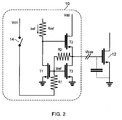
- the bias circuit 10 comprises first T1 and second T2 transistors which are scaled versions of a RF transistor 12 to be biased.
- the first T1 and second T2 transistors are provided in a looped arrangement, similar to that shown in Fig. 1 , wherein the drain of the first transistor T1 is connected to a current source Iref.
- the voltage source Vdd is connected to the drain of the second transistor T2 and the gate of the second transistor T2 is connected to the drain of the first transistor T1.
- the source of the second transistor T2 provides the output Vbias of the bias circuit 10.
- the first transistor T1 acts as a reference, which has its bias point fixed by the reference current source IREF.
- the second transistor T2 operates as a voltage buffer for the first transistor T1, and provides current to the output (i.e. the RF transistor 12 to be biased) when necessary.
- the bias circuit 10 may need to charge the RF transistor 12 in order to increase the bias voltage Vbias.
- the looped arrangement of the first and second transistors T1 and T2 enables the voltage on the first transistor T1 to control the output bias voltage Vbias.
- the voltage output from the gate of the first transistor T1 is the class AB amplifier bias voltage (i.e. a reference voltage Vref).
- the bias circuit 10 employs a conventional current mirror arrangement (like that shown in Fig. 1 ) wherein the reference transistor is the first transistor T1 in which a current Iref is injected corresponding to the desired class AB bias level. Like in a conventional current mirror (similar to that shown in Fig. 1 ), current is supplied to the output by the second transistor T2. It will be appreciated that in the case of MOS transistors, there is no DC current.
- a third transistor T3 is connected between bias circuit output and ground, with the control terminal (i.e. the gate) of the third transistor T3 being connected to the gate of the first transistor T1.
- the gate of the first transistor T1 is connected to a switch via a first resistor R1, and connected to the output terminal (i.e. the source of the second transistor T2 via a second resistor R2.
- the switch 14 is adapted to selectively disconnect/connect the first resistor R1 to control voltage Vctrl.
- the switch 14 When used in class AB, the switch 14 is in an open configuration and the control voltage Vctrl is not connected to the gate of the first transistor T1 via the first resistor R1, and the third transistor T3 then acts as an active load for the current mirror.
- the switch 14 When used in class C, the switch 14 is in a closed configuration and the control voltage Vctrl is connected to the gate of the first transistor T1 via the first resistor R.
- the control voltage Vctrl translates through the first R1 and second R2 resistors into shift in voltage at the output terminal of the bias circuit (Vbias) and the third transistor T3 acts as a non-linear load.
- the third transistor T3 When used in a switching mode, the third transistor T3 allows quick discharging of the load capacitance without affecting the bias circuit consumption in steady state mode.
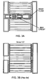
- FIG. 3A An exemplary layout of an embodiment within a ten cells discrete die is shown in Figure 3A , and the layout of a so called "sense FET" (widely used across base-station devices) within a ten cells discrete die is shown in Fig. 3B .
- the overall size of the bias circuit and the drain filter is very similar to the commonly used "sense FET". It is noted that, in case of a discrete die, increasing the size of the bias circuit translates to a decrease in the available space for the RF transistor, which in turn translates to a reduction of power density.
- FIG. 4 For the example of a discrete transistor, an example of transistor topology including a bias circuit according to an embodiment is illustrated in Figure 4 , wherein input prematch circuit includes a shunt inductance decoupled by a high value capacitor and a lowpass filter. Note that use of the shunt inductance with decoupling capacitor allows increasing RF bandwidth of the transistor, but is currently not used because it prevents fast switching of the bias (overall input capacitance too high). Embodiments allow use of wideband matching while maintaining fast switching capability.
- FIG. 5 Implementation of an embodiment within a regular discrete package is shown in Figure 5 .
- the leads usually dedicated to the sense FET connections are used as the input for the Class AB and control voltage Vctrl connections.
- the output leads are free for any kind of Video Bandwidth optimization at the output (the input Video Bandwidth being assured by the low impedance of the integrated bias).
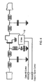
- Fig. 6 shows a conventional bias arrangement using a sense FET
- Fig. 6b shows a bias arrangement according to a proposed embodiment.
Landscapes
- Engineering & Computer Science (AREA)
- Power Engineering (AREA)
- Amplifiers (AREA)
Claims (13)
- Ein Vorspannungsschaltkreis für einen Transistor in einem Klasse C Verstärker, wobei der Vorspannungsschaltkreis aufweist:ein Klasse AB Verstärker Vorspannung Erzeugungsmittel, welches eingerichtet ist, eine Vorspannung (Vbias) an einem Ausgangsanschluss zu erzeugen; undeinen Transistor (T3), welcher zwischen den Ausgangsanschluss und eine erste Referenzspannung geschaltet ist, wobei der Steueranschluss des Transistors über einen Schalter (14) an eine zweite Referenzspannung (Vctrl) geschaltet ist,wobei ein Schließen des Schalters die zweite Referenzspannung an den Steueranschluss des Transistor schaltet, um eine Verschiebung in der Vorspannung zu bewirken, welche mittels des Klasse AB Verstärker Vorspannung Erzeugungsmittels erzeugt wird, um eine vorbestimmte Klasse C Vorspannung an dem Ausgangsanschluss zu erzielen.
- Der Vorspannungsschaltkreis gemäß Anspruch 1, wobei
ein erster Widerstand (R1) zwischen den Steueranschluss des Transistors (T3) und den Schalter (14) geschaltet ist, und
ein zweiter Widerstand (R2) zwischen den Steueranschluss des Transistors (T3) und den Ausgangsanschluss geschaltet ist. - Der Vorspannungsschaltkreis gemäß irgendeinem der vorangehenden Ansprüche, wobei das Klasse AB Verstärker Vorspannung Erzeugungsmittel einen Stromspiegel Schaltkreis aufweist.
- Der Vorspannungsschaltkreis gemäß Anspruch 3, wobei der Stromspiegel Schaltkreis aufweist
einen ersten (T1) und einen zweiten (T2) MOS Transistor, welche in einer Schleifenanordnung bereitgestellt sind, wobei der Drain des ersten MOS Transistors (T1) an eine Stromquelle IREF geschaltet ist, wobei eine Spannungsquelle (Vdd) an den Drain des zweiten MOS Transistors (T2) geschaltet ist, und wobei das Gate des zweiten MOS Transistors (T2) an den Drain des ersten MOS Transistors (T1) geschaltet ist, so dass die Quelle des zweiten MOS Transistors (T2) die Vorspannung bereitstellt. - Der Vorspannungsschaltkreis gemäß irgendeinem vorangehenden Anspruch, wobei der Vorspannungsschaltkreis ein integrierter Schaltkreis ist.
- Der Vorspannungsschaltkreis gemäß Anspruch 5, wobei der Vorspannungsschaltkreis auf demselben Schaltkreis integriert ist wie der Transistor, welcher vorzuspannen ist.
- Der Vorspannungsschaltkreis gemäß Anspruch 5 oder 6, wobei die zweite Referenzspannung (Vctrl) dem Vorspannungsschaltkreis extern bereitgestellt ist.
- Der Vorspannungsschaltkreis gemäß irgendeinem vorangehenden Anspruch, wobei die erste Referenzspannung eine Masse Spannung ist.
- Ein Doherty Verstärker Vorspannungsschaltkreis aufweisend einen Vorspannungsschaltkreis gemäß irgendeinem vorangehenden Anspruch.
- Ein Radiofrequenz Verstärkerschaltkreis aufweisend einen Vorspannungsschaltkreis gemäß irgendeinem der Ansprüche 1 bis 8.
- Ein Verfahren zum Vorspannen eines Transistors in einem Klasse C Verstärker, unter Verwendung eines Vorspannungsschaltkreises, welcher aufweist
ein Klasse AB Verstärker Vorspannung Erzeugungsmittel; und
einen Transistor (T3), welcher zwischen den Ausgangsanschluss und eine erste Referenzspannung geschaltet ist, wobei der Steueranschluss des Transistors über einen Schalter (14) an eine zweite Referenzspannung (Vctrl) geschaltet ist, wobei das Verfahren die Schritte aufweist:Erzeugen einer Vorspannung (Vbias) an einem Ausgangsanschluss des Vorspannungsschaltkreises unter Verwendung des Klasse AB Verstärker Vorspannung Erzeugungsmittels; undAktivieren des Schalters, um die zweite Referenzspannung an den Steueranschluss des Transistors zu schalten, um eine Verschiebung in der Vorspannung zu bewirken, welche mittels des Klasse AB Verstärker Vorspannung Erzeugungsmittels erzeugt wird, um eine vorbestimmte Klasse C Vorspannung an dem Ausgangsanschluss zu erzielen. - Ein Computer Programm Produkt zum Vorspannen eines Transistors in einem Klasse C Verstärker, welcher einen Vorspannungsschaltkreis verwendet, welcher aufweist:ein Klasse AB Verstärker Vorspannung Erzeugungsmittel; undeinen Transistor, welcher zwischen den Ausgangsanschluss und eine erste Referenzspannung geschaltet ist, wobei der Steueranschluss des Transistors über einen Schalter an eine zweite Referenzspannung geschaltet ist, wobei das Computer Programm Produkt ein computer-lesbares Speichermedium aufweist, welches damit einen computerlesbaren Programmcode verkörpert hat, wobei der computer-lesbare Programmcode konfiguriert ist, alle der Schritte gemäß Anspruch 11 auszuführen.
- Ein Computer System zum Vorspannen eines Transistors in einem Klasse C Verstärker, wobei das System aufweist:ein Computer Programm Produkt gemäß Anspruch 12; undeinen oder mehr Prozessoren, welche eingerichtet sind, alle der Schritte gemäß Anspruch 11 auszuführen.
Priority Applications (2)
| Application Number | Priority Date | Filing Date | Title |
|---|---|---|---|
| EP13290021.8A EP2760130B1 (de) | 2013-01-28 | 2013-01-28 | Bias-Schaltung |
| US14/164,484 US8854143B2 (en) | 2013-01-28 | 2014-01-27 | Bias circuit |
Applications Claiming Priority (1)
| Application Number | Priority Date | Filing Date | Title |
|---|---|---|---|
| EP13290021.8A EP2760130B1 (de) | 2013-01-28 | 2013-01-28 | Bias-Schaltung |
Publications (2)
| Publication Number | Publication Date |
|---|---|
| EP2760130A1 EP2760130A1 (de) | 2014-07-30 |
| EP2760130B1 true EP2760130B1 (de) | 2015-07-01 |
Family
ID=47722196
Family Applications (1)
| Application Number | Title | Priority Date | Filing Date |
|---|---|---|---|
| EP13290021.8A Not-in-force EP2760130B1 (de) | 2013-01-28 | 2013-01-28 | Bias-Schaltung |
Country Status (2)
| Country | Link |
|---|---|
| US (1) | US8854143B2 (de) |
| EP (1) | EP2760130B1 (de) |
Families Citing this family (4)
| Publication number | Priority date | Publication date | Assignee | Title |
|---|---|---|---|---|
| EP2879174B1 (de) * | 2013-11-29 | 2021-09-08 | Ampleon Netherlands B.V. | HF-Leistungstransistorvorrichtung im Gehäuse mit angrenzenden Masseleitungen und Videoleitung zum Verbinden von Entkopplungskondensatoren, HF-Leistungsverstärker |
| US9941842B2 (en) * | 2015-01-16 | 2018-04-10 | Qualcomm Incorporated | Amplifier bias circuit |
| US9722546B2 (en) | 2015-07-29 | 2017-08-01 | Avago Technologies General Ip (Singapore) Pte. Ltd. | Bias circuit for low quiescent current amplifier |
| CN119382633B (zh) * | 2024-10-12 | 2025-09-05 | 睿思微系统(烟台)有限公司 | Doherty功率放大器的有源动态偏置电路、Doherty功放电路及模组 |
Family Cites Families (10)
| Publication number | Priority date | Publication date | Assignee | Title |
|---|---|---|---|---|
| US5060294A (en) * | 1990-07-05 | 1991-10-22 | Motorola, Inc. | Dual mode power amplifier for radiotelephone |
| US6753734B2 (en) * | 2001-06-06 | 2004-06-22 | Anadigics, Inc. | Multi-mode amplifier bias circuit |
| US6917246B2 (en) | 2001-09-10 | 2005-07-12 | Skyworks Solutions, Inc. | Doherty bias circuit to dynamically compensate for process and environmental variations |
| US6873211B1 (en) * | 2003-09-10 | 2005-03-29 | Skyworks Solutions, Inc. | Multi-mode bias circuit for power amplifiers |
| WO2007003219A1 (en) | 2005-06-30 | 2007-01-11 | Freescale Semiconductor, Inc | Wireless communication unit, integrated circuit and biasing circuit therefor |
| WO2008041063A1 (en) | 2006-10-03 | 2008-04-10 | Freescale Semiconductor, Inc. | Bias circuit and method for biasing a transistor in a class c amplifier |
| US8812052B2 (en) * | 2007-02-27 | 2014-08-19 | Qualcomm Incorporated | SPS receiver with adjustable linearity |
| US7760026B2 (en) * | 2008-03-05 | 2010-07-20 | Skyworks Solutions, Inc. | Switched capacitor voltage converter for a power amplifier |
| JP5245887B2 (ja) * | 2009-02-09 | 2013-07-24 | 富士通セミコンダクター株式会社 | 増幅器 |
| CN102474231A (zh) * | 2010-03-10 | 2012-05-23 | 松下电器产业株式会社 | 可变增益放大器 |
-
2013
- 2013-01-28 EP EP13290021.8A patent/EP2760130B1/de not_active Not-in-force
-
2014
- 2014-01-27 US US14/164,484 patent/US8854143B2/en active Active
Also Published As
| Publication number | Publication date |
|---|---|
| EP2760130A1 (de) | 2014-07-30 |
| US8854143B2 (en) | 2014-10-07 |
| US20140210557A1 (en) | 2014-07-31 |
Similar Documents
| Publication | Publication Date | Title |
|---|---|---|
| CN109428557B (zh) | 功率放大电路 | |
| US20220413538A1 (en) | Bias circuit and amplifier | |
| TWI509979B (zh) | 電子系統、射頻功率放大器及其偏壓點動態調整方法 | |
| JP2006500884A (ja) | 切換可能な可変出力電力レベルを有する飽和電力増幅器 | |
| US11444582B2 (en) | Power amplifier circuit | |
| US9722546B2 (en) | Bias circuit for low quiescent current amplifier | |
| US11290060B2 (en) | Bias circuit | |
| CN116896331A (zh) | 功率放大器系统 | |
| EP2760130B1 (de) | Bias-Schaltung | |
| CN109586674B (zh) | 功率放大电路 | |
| JP2020057934A (ja) | 電力増幅回路 | |
| US10910999B2 (en) | Bias circuit | |
| TWI501543B (zh) | 電子系統、射頻功率放大器及其偏壓點自我調整方法 | |
| US20250226802A1 (en) | Power amplifier using multi-path common-mode feedback loop | |
| US9337778B2 (en) | Adaptive bias circuit and power amplifier | |
| US20140354363A1 (en) | Power amplifier | |
| US9065389B2 (en) | Radio frequency power amplifier with no reference voltage for biasing and electronic system | |
| JP2019205006A (ja) | 電力増幅回路 | |
| CN116979906A (zh) | 通过使用交叉耦合组件的偏置控制使差分射频功率放大器线性化 | |
| TW201824740A (zh) | 放大電路 | |
| US8482355B2 (en) | Power amplifier | |
| KR101891619B1 (ko) | 질화갈륨 집적회로 증폭기의 선형화 바이어스 회로 기술 | |
| JP2021005818A (ja) | 電力増幅回路 | |
| JP5714958B2 (ja) | 増幅回路 | |
| US11296655B2 (en) | Power amplifier biasing network providing gain expansion |
Legal Events
| Date | Code | Title | Description |
|---|---|---|---|
| PUAI | Public reference made under article 153(3) epc to a published international application that has entered the european phase |
Free format text: ORIGINAL CODE: 0009012 |
|
| 17P | Request for examination filed |
Effective date: 20131031 |
|
| AK | Designated contracting states |
Kind code of ref document: A1 Designated state(s): AL AT BE BG CH CY CZ DE DK EE ES FI FR GB GR HR HU IE IS IT LI LT LU LV MC MK MT NL NO PL PT RO RS SE SI SK SM TR |
|
| AX | Request for extension of the european patent |
Extension state: BA ME |
|
| GRAP | Despatch of communication of intention to grant a patent |
Free format text: ORIGINAL CODE: EPIDOSNIGR1 |
|
| RIC1 | Information provided on ipc code assigned before grant |
Ipc: H03F 1/02 20060101AFI20141027BHEP Ipc: H03F 3/19 20060101ALI20141027BHEP Ipc: H03F 1/30 20060101ALI20141027BHEP |
|
| INTG | Intention to grant announced |
Effective date: 20141121 |
|
| RBV | Designated contracting states (corrected) |
Designated state(s): AL AT BE BG CH CY CZ DE DK EE ES FI FR GB GR HR HU IE IS IT LI LT LU LV MC MK MT NL NO PL PT RO RS SE SI SK SM TR |
|
| REG | Reference to a national code |
Ref country code: DE Ref legal event code: R079 Ref document number: 602013002137 Country of ref document: DE Free format text: PREVIOUS MAIN CLASS: H03F0001020000 Ipc: H01L0023660000 |
|
| GRAP | Despatch of communication of intention to grant a patent |
Free format text: ORIGINAL CODE: EPIDOSNIGR1 |
|
| GRAS | Grant fee paid |
Free format text: ORIGINAL CODE: EPIDOSNIGR3 |
|
| RIC1 | Information provided on ipc code assigned before grant |
Ipc: H03F 1/30 20060101ALI20150417BHEP Ipc: H03F 3/19 20060101ALI20150417BHEP Ipc: H01L 23/66 20060101AFI20150417BHEP Ipc: H03F 1/02 20060101ALI20150417BHEP |
|
| GRAA | (expected) grant |
Free format text: ORIGINAL CODE: 0009210 |
|
| INTG | Intention to grant announced |
Effective date: 20150505 |
|
| AK | Designated contracting states |
Kind code of ref document: B1 Designated state(s): AL AT BE BG CH CY CZ DE DK EE ES FI FR GB GR HR HU IE IS IT LI LT LU LV MC MK MT NL NO PL PT RO RS SE SI SK SM TR |
|
| REG | Reference to a national code |
Ref country code: GB Ref legal event code: FG4D |
|
| REG | Reference to a national code |
Ref country code: AT Ref legal event code: REF Ref document number: 734411 Country of ref document: AT Kind code of ref document: T Effective date: 20150715 Ref country code: CH Ref legal event code: EP |
|
| REG | Reference to a national code |
Ref country code: IE Ref legal event code: FG4D |
|
| REG | Reference to a national code |
Ref country code: DE Ref legal event code: R096 Ref document number: 602013002137 Country of ref document: DE |
|
| REG | Reference to a national code |
Ref country code: FR Ref legal event code: TP Owner name: SAMBA HOLDCO NETHERLANDS BV, NL Effective date: 20150930 |
|
| REG | Reference to a national code |
Ref country code: AT Ref legal event code: MK05 Ref document number: 734411 Country of ref document: AT Kind code of ref document: T Effective date: 20150701 |
|
| REG | Reference to a national code |
Ref country code: GB Ref legal event code: 732E Free format text: REGISTERED BETWEEN 20151029 AND 20151104 |
|
| REG | Reference to a national code |
Ref country code: DE Ref legal event code: R081 Ref document number: 602013002137 Country of ref document: DE Owner name: SAMBA HOLDCO NETHERLANDS B.V., NL Free format text: FORMER OWNER: NXP B.V., EINDHOVEN, NL Ref country code: DE Ref legal event code: R081 Ref document number: 602013002137 Country of ref document: DE Owner name: AMPLEON NETHERLANDS B.V., NL Free format text: FORMER OWNER: NXP B.V., EINDHOVEN, NL |
|
| REG | Reference to a national code |
Ref country code: NL Ref legal event code: MP Effective date: 20150701 |
|
| REG | Reference to a national code |
Ref country code: LT Ref legal event code: MG4D |
|
| REG | Reference to a national code |
Ref country code: FR Ref legal event code: PLFP Year of fee payment: 4 |
|
| PG25 | Lapsed in a contracting state [announced via postgrant information from national office to epo] |
Ref country code: NO Free format text: LAPSE BECAUSE OF FAILURE TO SUBMIT A TRANSLATION OF THE DESCRIPTION OR TO PAY THE FEE WITHIN THE PRESCRIBED TIME-LIMIT Effective date: 20151001 Ref country code: FI Free format text: LAPSE BECAUSE OF FAILURE TO SUBMIT A TRANSLATION OF THE DESCRIPTION OR TO PAY THE FEE WITHIN THE PRESCRIBED TIME-LIMIT Effective date: 20150701 Ref country code: LT Free format text: LAPSE BECAUSE OF FAILURE TO SUBMIT A TRANSLATION OF THE DESCRIPTION OR TO PAY THE FEE WITHIN THE PRESCRIBED TIME-LIMIT Effective date: 20150701 Ref country code: GR Free format text: LAPSE BECAUSE OF FAILURE TO SUBMIT A TRANSLATION OF THE DESCRIPTION OR TO PAY THE FEE WITHIN THE PRESCRIBED TIME-LIMIT Effective date: 20151002 Ref country code: LV Free format text: LAPSE BECAUSE OF FAILURE TO SUBMIT A TRANSLATION OF THE DESCRIPTION OR TO PAY THE FEE WITHIN THE PRESCRIBED TIME-LIMIT Effective date: 20150701 |
|
| PG25 | Lapsed in a contracting state [announced via postgrant information from national office to epo] |
Ref country code: SE Free format text: LAPSE BECAUSE OF FAILURE TO SUBMIT A TRANSLATION OF THE DESCRIPTION OR TO PAY THE FEE WITHIN THE PRESCRIBED TIME-LIMIT Effective date: 20150701 Ref country code: RS Free format text: LAPSE BECAUSE OF FAILURE TO SUBMIT A TRANSLATION OF THE DESCRIPTION OR TO PAY THE FEE WITHIN THE PRESCRIBED TIME-LIMIT Effective date: 20150701 Ref country code: PT Free format text: LAPSE BECAUSE OF FAILURE TO SUBMIT A TRANSLATION OF THE DESCRIPTION OR TO PAY THE FEE WITHIN THE PRESCRIBED TIME-LIMIT Effective date: 20151102 Ref country code: PL Free format text: LAPSE BECAUSE OF FAILURE TO SUBMIT A TRANSLATION OF THE DESCRIPTION OR TO PAY THE FEE WITHIN THE PRESCRIBED TIME-LIMIT Effective date: 20150701 Ref country code: ES Free format text: LAPSE BECAUSE OF FAILURE TO SUBMIT A TRANSLATION OF THE DESCRIPTION OR TO PAY THE FEE WITHIN THE PRESCRIBED TIME-LIMIT Effective date: 20150701 Ref country code: AT Free format text: LAPSE BECAUSE OF FAILURE TO SUBMIT A TRANSLATION OF THE DESCRIPTION OR TO PAY THE FEE WITHIN THE PRESCRIBED TIME-LIMIT Effective date: 20150701 Ref country code: HR Free format text: LAPSE BECAUSE OF FAILURE TO SUBMIT A TRANSLATION OF THE DESCRIPTION OR TO PAY THE FEE WITHIN THE PRESCRIBED TIME-LIMIT Effective date: 20150701 Ref country code: IS Free format text: LAPSE BECAUSE OF FAILURE TO SUBMIT A TRANSLATION OF THE DESCRIPTION OR TO PAY THE FEE WITHIN THE PRESCRIBED TIME-LIMIT Effective date: 20151101 |
|
| REG | Reference to a national code |
Ref country code: DE Ref legal event code: R081 Ref document number: 602013002137 Country of ref document: DE Owner name: AMPLEON NETHERLANDS B.V., NL Free format text: FORMER OWNER: SAMBA HOLDCO NETHERLANDS B.V., EINDHOVEN, NL |
|
| REG | Reference to a national code |
Ref country code: DE Ref legal event code: R097 Ref document number: 602013002137 Country of ref document: DE |
|
| PG25 | Lapsed in a contracting state [announced via postgrant information from national office to epo] |
Ref country code: IT Free format text: LAPSE BECAUSE OF FAILURE TO SUBMIT A TRANSLATION OF THE DESCRIPTION OR TO PAY THE FEE WITHIN THE PRESCRIBED TIME-LIMIT Effective date: 20150701 Ref country code: SK Free format text: LAPSE BECAUSE OF FAILURE TO SUBMIT A TRANSLATION OF THE DESCRIPTION OR TO PAY THE FEE WITHIN THE PRESCRIBED TIME-LIMIT Effective date: 20150701 Ref country code: EE Free format text: LAPSE BECAUSE OF FAILURE TO SUBMIT A TRANSLATION OF THE DESCRIPTION OR TO PAY THE FEE WITHIN THE PRESCRIBED TIME-LIMIT Effective date: 20150701 Ref country code: DK Free format text: LAPSE BECAUSE OF FAILURE TO SUBMIT A TRANSLATION OF THE DESCRIPTION OR TO PAY THE FEE WITHIN THE PRESCRIBED TIME-LIMIT Effective date: 20150701 Ref country code: CZ Free format text: LAPSE BECAUSE OF FAILURE TO SUBMIT A TRANSLATION OF THE DESCRIPTION OR TO PAY THE FEE WITHIN THE PRESCRIBED TIME-LIMIT Effective date: 20150701 |
|
| PLBE | No opposition filed within time limit |
Free format text: ORIGINAL CODE: 0009261 |
|
| STAA | Information on the status of an ep patent application or granted ep patent |
Free format text: STATUS: NO OPPOSITION FILED WITHIN TIME LIMIT |
|
| PG25 | Lapsed in a contracting state [announced via postgrant information from national office to epo] |
Ref country code: BE Free format text: LAPSE BECAUSE OF NON-PAYMENT OF DUE FEES Effective date: 20160131 Ref country code: RO Free format text: LAPSE BECAUSE OF FAILURE TO SUBMIT A TRANSLATION OF THE DESCRIPTION OR TO PAY THE FEE WITHIN THE PRESCRIBED TIME-LIMIT Effective date: 20150701 |
|
| 26N | No opposition filed |
Effective date: 20160404 |
|
| REG | Reference to a national code |
Ref country code: FR Ref legal event code: CA Effective date: 20160721 Ref country code: FR Ref legal event code: CD Owner name: AMPLEON NETHERLANDS B.V., NL Effective date: 20160721 |
|
| PG25 | Lapsed in a contracting state [announced via postgrant information from national office to epo] |
Ref country code: SI Free format text: LAPSE BECAUSE OF FAILURE TO SUBMIT A TRANSLATION OF THE DESCRIPTION OR TO PAY THE FEE WITHIN THE PRESCRIBED TIME-LIMIT Effective date: 20150701 Ref country code: LU Free format text: LAPSE BECAUSE OF FAILURE TO SUBMIT A TRANSLATION OF THE DESCRIPTION OR TO PAY THE FEE WITHIN THE PRESCRIBED TIME-LIMIT Effective date: 20160128 |
|
| REG | Reference to a national code |
Ref country code: CH Ref legal event code: PL |
|
| PG25 | Lapsed in a contracting state [announced via postgrant information from national office to epo] |
Ref country code: MC Free format text: LAPSE BECAUSE OF FAILURE TO SUBMIT A TRANSLATION OF THE DESCRIPTION OR TO PAY THE FEE WITHIN THE PRESCRIBED TIME-LIMIT Effective date: 20150701 |
|
| PG25 | Lapsed in a contracting state [announced via postgrant information from national office to epo] |
Ref country code: CH Free format text: LAPSE BECAUSE OF NON-PAYMENT OF DUE FEES Effective date: 20160131 Ref country code: LI Free format text: LAPSE BECAUSE OF NON-PAYMENT OF DUE FEES Effective date: 20160131 |
|
| REG | Reference to a national code |
Ref country code: IE Ref legal event code: MM4A |
|
| PG25 | Lapsed in a contracting state [announced via postgrant information from national office to epo] |
Ref country code: BE Free format text: LAPSE BECAUSE OF FAILURE TO SUBMIT A TRANSLATION OF THE DESCRIPTION OR TO PAY THE FEE WITHIN THE PRESCRIBED TIME-LIMIT Effective date: 20150701 |
|
| REG | Reference to a national code |
Ref country code: FR Ref legal event code: PLFP Year of fee payment: 5 |
|
| PG25 | Lapsed in a contracting state [announced via postgrant information from national office to epo] |
Ref country code: IE Free format text: LAPSE BECAUSE OF NON-PAYMENT OF DUE FEES Effective date: 20160128 |
|
| PG25 | Lapsed in a contracting state [announced via postgrant information from national office to epo] |
Ref country code: NL Free format text: LAPSE BECAUSE OF FAILURE TO SUBMIT A TRANSLATION OF THE DESCRIPTION OR TO PAY THE FEE WITHIN THE PRESCRIBED TIME-LIMIT Effective date: 20150701 |
|
| PG25 | Lapsed in a contracting state [announced via postgrant information from national office to epo] |
Ref country code: MT Free format text: LAPSE BECAUSE OF FAILURE TO SUBMIT A TRANSLATION OF THE DESCRIPTION OR TO PAY THE FEE WITHIN THE PRESCRIBED TIME-LIMIT Effective date: 20150701 |
|
| REG | Reference to a national code |
Ref country code: FR Ref legal event code: PLFP Year of fee payment: 6 |
|
| PG25 | Lapsed in a contracting state [announced via postgrant information from national office to epo] |
Ref country code: CY Free format text: LAPSE BECAUSE OF FAILURE TO SUBMIT A TRANSLATION OF THE DESCRIPTION OR TO PAY THE FEE WITHIN THE PRESCRIBED TIME-LIMIT Effective date: 20150701 Ref country code: SM Free format text: LAPSE BECAUSE OF FAILURE TO SUBMIT A TRANSLATION OF THE DESCRIPTION OR TO PAY THE FEE WITHIN THE PRESCRIBED TIME-LIMIT Effective date: 20150701 Ref country code: HU Free format text: LAPSE BECAUSE OF FAILURE TO SUBMIT A TRANSLATION OF THE DESCRIPTION OR TO PAY THE FEE WITHIN THE PRESCRIBED TIME-LIMIT; INVALID AB INITIO Effective date: 20130128 |
|
| PG25 | Lapsed in a contracting state [announced via postgrant information from national office to epo] |
Ref country code: TR Free format text: LAPSE BECAUSE OF FAILURE TO SUBMIT A TRANSLATION OF THE DESCRIPTION OR TO PAY THE FEE WITHIN THE PRESCRIBED TIME-LIMIT Effective date: 20150701 Ref country code: MT Free format text: LAPSE BECAUSE OF FAILURE TO SUBMIT A TRANSLATION OF THE DESCRIPTION OR TO PAY THE FEE WITHIN THE PRESCRIBED TIME-LIMIT Effective date: 20160131 Ref country code: MK Free format text: LAPSE BECAUSE OF FAILURE TO SUBMIT A TRANSLATION OF THE DESCRIPTION OR TO PAY THE FEE WITHIN THE PRESCRIBED TIME-LIMIT Effective date: 20150701 |
|
| PG25 | Lapsed in a contracting state [announced via postgrant information from national office to epo] |
Ref country code: BG Free format text: LAPSE BECAUSE OF FAILURE TO SUBMIT A TRANSLATION OF THE DESCRIPTION OR TO PAY THE FEE WITHIN THE PRESCRIBED TIME-LIMIT Effective date: 20150701 |
|
| PG25 | Lapsed in a contracting state [announced via postgrant information from national office to epo] |
Ref country code: AL Free format text: LAPSE BECAUSE OF FAILURE TO SUBMIT A TRANSLATION OF THE DESCRIPTION OR TO PAY THE FEE WITHIN THE PRESCRIBED TIME-LIMIT Effective date: 20150701 |
|
| PGFP | Annual fee paid to national office [announced via postgrant information from national office to epo] |
Ref country code: FR Payment date: 20210125 Year of fee payment: 9 |
|
| PGFP | Annual fee paid to national office [announced via postgrant information from national office to epo] |
Ref country code: DE Payment date: 20210127 Year of fee payment: 9 Ref country code: GB Payment date: 20210128 Year of fee payment: 9 |
|
| REG | Reference to a national code |
Ref country code: DE Ref legal event code: R119 Ref document number: 602013002137 Country of ref document: DE |
|
| GBPC | Gb: european patent ceased through non-payment of renewal fee |
Effective date: 20220128 |
|
| PG25 | Lapsed in a contracting state [announced via postgrant information from national office to epo] |
Ref country code: GB Free format text: LAPSE BECAUSE OF NON-PAYMENT OF DUE FEES Effective date: 20220128 Ref country code: DE Free format text: LAPSE BECAUSE OF NON-PAYMENT OF DUE FEES Effective date: 20220802 |
|
| PG25 | Lapsed in a contracting state [announced via postgrant information from national office to epo] |
Ref country code: FR Free format text: LAPSE BECAUSE OF NON-PAYMENT OF DUE FEES Effective date: 20220131 |