EP2760121A1 - Electronic circuit - Google Patents
Electronic circuit Download PDFInfo
- Publication number
- EP2760121A1 EP2760121A1 EP12833355.6A EP12833355A EP2760121A1 EP 2760121 A1 EP2760121 A1 EP 2760121A1 EP 12833355 A EP12833355 A EP 12833355A EP 2760121 A1 EP2760121 A1 EP 2760121A1
- Authority
- EP
- European Patent Office
- Prior art keywords
- power supply
- supply terminal
- bus bar
- inductance
- mosfet
- Prior art date
- Legal status (The legal status is an assumption and is not a legal conclusion. Google has not performed a legal analysis and makes no representation as to the accuracy of the status listed.)
- Granted
Links
Images



Classifications
-
- H—ELECTRICITY
- H02—GENERATION; CONVERSION OR DISTRIBUTION OF ELECTRIC POWER
- H02M—APPARATUS FOR CONVERSION BETWEEN AC AND AC, BETWEEN AC AND DC, OR BETWEEN DC AND DC, AND FOR USE WITH MAINS OR SIMILAR POWER SUPPLY SYSTEMS; CONVERSION OF DC OR AC INPUT POWER INTO SURGE OUTPUT POWER; CONTROL OR REGULATION THEREOF
- H02M1/00—Details of apparatus for conversion
- H02M1/32—Means for protecting converters other than automatic disconnection
- H02M1/34—Snubber circuits
-
- H—ELECTRICITY
- H02—GENERATION; CONVERSION OR DISTRIBUTION OF ELECTRIC POWER
- H02M—APPARATUS FOR CONVERSION BETWEEN AC AND AC, BETWEEN AC AND DC, OR BETWEEN DC AND DC, AND FOR USE WITH MAINS OR SIMILAR POWER SUPPLY SYSTEMS; CONVERSION OF DC OR AC INPUT POWER INTO SURGE OUTPUT POWER; CONTROL OR REGULATION THEREOF
- H02M7/00—Conversion of AC power input into DC power output; Conversion of DC power input into AC power output
- H02M7/003—Constructional details, e.g. physical layout, assembly, wiring or busbar connections
-
- H—ELECTRICITY
- H02—GENERATION; CONVERSION OR DISTRIBUTION OF ELECTRIC POWER
- H02M—APPARATUS FOR CONVERSION BETWEEN AC AND AC, BETWEEN AC AND DC, OR BETWEEN DC AND DC, AND FOR USE WITH MAINS OR SIMILAR POWER SUPPLY SYSTEMS; CONVERSION OF DC OR AC INPUT POWER INTO SURGE OUTPUT POWER; CONTROL OR REGULATION THEREOF
- H02M7/00—Conversion of AC power input into DC power output; Conversion of DC power input into AC power output
- H02M7/42—Conversion of DC power input into AC power output without possibility of reversal
- H02M7/44—Conversion of DC power input into AC power output without possibility of reversal by static converters
- H02M7/48—Conversion of DC power input into AC power output without possibility of reversal by static converters using discharge tubes with control electrode or semiconductor devices with control electrode
- H02M7/53—Conversion of DC power input into AC power output without possibility of reversal by static converters using discharge tubes with control electrode or semiconductor devices with control electrode using devices of a triode or transistor type requiring continuous application of a control signal
- H02M7/537—Conversion of DC power input into AC power output without possibility of reversal by static converters using discharge tubes with control electrode or semiconductor devices with control electrode using devices of a triode or transistor type requiring continuous application of a control signal using semiconductor devices only, e.g. single switched pulse inverters
-
- H—ELECTRICITY
- H02—GENERATION; CONVERSION OR DISTRIBUTION OF ELECTRIC POWER
- H02M—APPARATUS FOR CONVERSION BETWEEN AC AND AC, BETWEEN AC AND DC, OR BETWEEN DC AND DC, AND FOR USE WITH MAINS OR SIMILAR POWER SUPPLY SYSTEMS; CONVERSION OF DC OR AC INPUT POWER INTO SURGE OUTPUT POWER; CONTROL OR REGULATION THEREOF
- H02M7/00—Conversion of AC power input into DC power output; Conversion of DC power input into AC power output
- H02M7/42—Conversion of DC power input into AC power output without possibility of reversal
- H02M7/44—Conversion of DC power input into AC power output without possibility of reversal by static converters
- H02M7/48—Conversion of DC power input into AC power output without possibility of reversal by static converters using discharge tubes with control electrode or semiconductor devices with control electrode
- H02M7/53—Conversion of DC power input into AC power output without possibility of reversal by static converters using discharge tubes with control electrode or semiconductor devices with control electrode using devices of a triode or transistor type requiring continuous application of a control signal
- H02M7/537—Conversion of DC power input into AC power output without possibility of reversal by static converters using discharge tubes with control electrode or semiconductor devices with control electrode using devices of a triode or transistor type requiring continuous application of a control signal using semiconductor devices only, e.g. single switched pulse inverters
- H02M7/5387—Conversion of DC power input into AC power output without possibility of reversal by static converters using discharge tubes with control electrode or semiconductor devices with control electrode using devices of a triode or transistor type requiring continuous application of a control signal using semiconductor devices only, e.g. single switched pulse inverters in a bridge configuration
-
- H—ELECTRICITY
- H02—GENERATION; CONVERSION OR DISTRIBUTION OF ELECTRIC POWER
- H02M—APPARATUS FOR CONVERSION BETWEEN AC AND AC, BETWEEN AC AND DC, OR BETWEEN DC AND DC, AND FOR USE WITH MAINS OR SIMILAR POWER SUPPLY SYSTEMS; CONVERSION OF DC OR AC INPUT POWER INTO SURGE OUTPUT POWER; CONTROL OR REGULATION THEREOF
- H02M1/00—Details of apparatus for conversion
- H02M1/32—Means for protecting converters other than automatic disconnection
- H02M1/34—Snubber circuits
- H02M1/346—Passive non-dissipative snubbers
-
- H—ELECTRICITY
- H02—GENERATION; CONVERSION OR DISTRIBUTION OF ELECTRIC POWER
- H02M—APPARATUS FOR CONVERSION BETWEEN AC AND AC, BETWEEN AC AND DC, OR BETWEEN DC AND DC, AND FOR USE WITH MAINS OR SIMILAR POWER SUPPLY SYSTEMS; CONVERSION OF DC OR AC INPUT POWER INTO SURGE OUTPUT POWER; CONTROL OR REGULATION THEREOF
- H02M1/00—Details of apparatus for conversion
- H02M1/32—Means for protecting converters other than automatic disconnection
- H02M1/34—Snubber circuits
- H02M1/348—Passive dissipative snubbers
-
- Y—GENERAL TAGGING OF NEW TECHNOLOGICAL DEVELOPMENTS; GENERAL TAGGING OF CROSS-SECTIONAL TECHNOLOGIES SPANNING OVER SEVERAL SECTIONS OF THE IPC; TECHNICAL SUBJECTS COVERED BY FORMER USPC CROSS-REFERENCE ART COLLECTIONS [XRACs] AND DIGESTS
- Y02—TECHNOLOGIES OR APPLICATIONS FOR MITIGATION OR ADAPTATION AGAINST CLIMATE CHANGE
- Y02B—CLIMATE CHANGE MITIGATION TECHNOLOGIES RELATED TO BUILDINGS, e.g. HOUSING, HOUSE APPLIANCES OR RELATED END-USER APPLICATIONS
- Y02B70/00—Technologies for an efficient end-user side electric power management and consumption
- Y02B70/10—Technologies improving the efficiency by using switched-mode power supplies [SMPS], i.e. efficient power electronics conversion e.g. power factor correction or reduction of losses in power supplies or efficient standby modes
Definitions
- the present invention relates to an electronic circuit, such as a three-phase inverter circuit or an H bridge circuit.
- a MOSFET Metal-Oxide-Semiconductor Field Effect Transistor
- DMOSFET Double Diffused MOSFET
- IGBT Insulated Gate Bipolar Transistor
- a gate drive signal is supplied to a gate terminal of the MOSFET or of the IGBT through a gate resistor.
- FIG. 5 is a graph showing a relationship among gate resistance, switching loss (DMOS Eoff) caused when a DMOSFET is turned off, and surge voltage and showing a relationship among gate resistance, switching loss (IGBT Eoff) caused when an IGBT is turned off, and surge voltage.
- DMOS Eoff switching loss
- IGBT Eoff switching loss
- the gate resistance dependency of switching loss at the turn-off time is low. Additionally, in the IGBT, the amount of increase of the surge voltage is small with respect to an increase of the gate resistance. On the other hand, in the DMOSFET, the switching loss at the turn-off time can be made much smaller by reducing the gate resistance than in the IGBT. However, in the DMOSFET, if the gate resistance is reduced, the rate of change di/dt of a drain current at the turn-off time will become great, and therefore a great surge voltage will be generated.
- Patent Literature 1 discloses an arrangement in which, in a three-phase inverter circuit including six IGBTs, a snubber circuit is connected between a single DC input terminal P to which a collector of high-side IGBTs equivalent to three phases is connected and a single DC input terminal N to which an emitter of low-side IGBTs equivalent to three phases is connected, in order to restrain a surge voltage.
- An object of the present invention is to provide an electronic circuit capable of reducing the switching loss and capable of reducing the surge voltage when a MOSFET is turned off.
- the electronic circuit of the present invention is an electronic circuit having a plurality of series circuits each of which has two MOSFETs connected in series in which a first power supply terminal is connected to one end of each of the series circuits and in which a second power supply terminal is connected to an opposite end of each of the series circuits, and the electronic circuit is composed of a first bus bar one end of which is connected to each of the first power supply terminals and that forms a part of an external electric wire to connect the first power supply terminal to one terminal of a power source, a second bus bar one end of which is connected to each of the second power supply terminals and that forms a part of an external electric wire to connect the second power supply terminal to an opposite terminal of the power source, and a snubber circuit that is provided in each of the series circuits and that is connected between the first bus bar connected to the series circuit through the first power supply terminal and the second bus bar connected to the series circuit through the second power supply terminal.
- each of the snubber circuits is connected to a part of the corresponding first bus bar closer to the first power supply terminal, whereas an opposite end of each of the snubber circuits is connected to a part of the corresponding second bus bar closer to the second power supply terminal.
- the present invention includes a snubber circuit that is provided in each series circuit and that is connected between the first bus bar connected to the series circuit through the first power supply terminal and the second bus bar connected to the series circuit through the second power supply terminal, and therefore the surge voltage applied to a MOSFET when the MOSFET is turned off can be reduced.
- each snubber circuit is connected to a part of the corresponding first bus bar closer to the first power supply terminal, and therefore the inductance of an interval part between the connection position of the snubber circuit and the first power supply terminal in the first bus bar can be reduced.
- an opposite end of each snubber circuit is connected to a part of the corresponding second bus bar closer to the second power supply terminal, and therefore the inductance of an interval part between the connection position of the snubber circuit and the second power supply terminal in the second bus bar can be reduced.
- a sum of an inductance of an interval part between a connection point with one end of the snubber circuit and the first power supply terminal in the first bus bar, an inductance of an interval part between a connection point with an opposite end of the snubber circuit and the second power supply terminal in the second bus bar, and an inductance of the series circuit between the first power supply terminal and the second power supply terminal is 40 nH or less.
- the inductance that causes the generation of the surge voltage applied to the MOSFET that has been turned off can be reduced to be 40 nH or less, and therefore the switching loss at the turn-off time of the MOSFET can be reduced, and the surge voltage can be reduced.
- one end of the snubber circuit is connected between one end of the first bus bar closer to the first power supply terminal and a second position of the first bus bar located at a first predetermined distance with respect to a first position of the first bus bar nearest to an outer end of the first power supply terminal in a direction receding from the first power supply terminal.
- the first predetermined distance is set so that an inductance of a part of the first bus bar from the first position to the second position becomes equal to 6.25 nH or less.
- An opposite end of the snubber circuit is connected between one end of the second bus bar closer to the second power supply terminal and a fourth position located at a second predetermined distance with respect to a third position nearest to an outer end of the second power supply terminal in a direction receding from the second power supply terminal.
- the second predetermined distance is set so that an inductance of a part of the second bus bar from the third position to the fourth position becomes equal to 6.25 nH or less.
- the inductance that causes the generation of the surge voltage applied to the MOSFET that has been turned off can be reduced, and therefore the switching loss at the turn-off time of the MOSFET can be reduced, and the surge voltage can be reduced.
- each of the MOSFETs is a SiC-MOSFETmade of a semiconductormaterial composed chiefly of SiC.
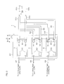
- FIG. 1 is an electric circuit diagram showing a three-phase inverter circuit 1 according to an embodiment of the present invention.
- This three-phase inverter circuit 1 is a circuit to drive a three-phase brushless motor 8 (hereinafter, referred to as an "electric motor").
- the electric motor 8 is composed of a stator that has a U-phase field coil 8U, a V-phase field coil 8V, and a W-phase field coil 8W and a rotor to which a permanent magnet is fixed.
- the three-phase inverter circuit 1 includes a U-phase module 3 that is used for a U phase, a V-phase module 4 that is used for a V phase, and a W-phase module 5 that is used for a W phase.
- the U-phase module 3 is composed of a first power supply terminal (P terminal) 31, a second power supply terminal (N terminal) 32, an output terminal (OUT terminal) 33, two gate terminals 34 and 37, two source terminals 35 and 38, and two source sense terminals 36 and 39.
- the V-phase module 4 is composed of a first power supply terminal (P terminal) 41, a second power supply terminal (N terminal) 42, an output terminal (OUT terminal) 43, two gate terminals 44 and 47, two source terminals 45 and 48, and two source sense terminals 46 and 49.
- the W-phase module 5 is composed of a first power supply terminal (P terminal) 51, a second power supply terminal (N terminal) 52, an output terminal (OUT terminal) 53, two gate terminals 54 and 57, two source terminals 55 and 58, and two source sense terminals 56 and 59.
- Each of the first power supply terminals 31, 41, and 51 of the modules 3, 4, and 5 is connected to a positive terminal of a power source (DC power source) 6 through an external electric wire. More specifically, the first power supply terminal 31 of the U-phase module 3 is connected to the positive terminal of the power source 6 through a first external electric wire 61. The first power supply terminal 41 of the V-phase module 4 is connected to an intermediate part of the first external electric wire 61 through a second external electric wire 62. The first power supply terminal 51 of the W-phase module 5 is connected to the intermediate part of the first external electric wire 61 through a third external electric wire 63.
- Each of the second power supply terminals 32, 42, and 52 of the modules 3, 4, and 5 is connected to a negative terminal of the power source 6 through an external electric wire. More specifically, the second power supply terminal 32 of the U-phase module 3 is connected to the negative terminal of the power source 6 through a fourth external electric wire 64. The second power supply terminal 42 of the V-phase module 4 is connected to an intermediate part of the fourth external electric wire 64 through a fifth external electric wire 65. The second power supply terminal 52 of the W-phase module 5 is connected to the intermediate part of the fourth external electric wire 64 through a sixth external electric wire 66. An inductance parasitizes each of the external electric wires 61 to 66.
- a smoothing capacitor 7 is connected to the power source 6 in parallel.
- the output terminals 33, 43, and 53 of the modules 3, 4, and 5 are connected to a U-phase field winding 8U, a V-phase field winding 8V, and a W-phase field winding 8W of the electric motor 8 through seventh, eighth, and ninth external electric wires 67, 68, and 69, respectively.
- a control unit (not shown) is connected to each of the gate terminals 34, 37, 44, 47, 54, 57 and to each of the source sense terminals 36, 39, 46, 49, 56, and 59 of the modules 3, 4, and 5.
- the control unit allows a gate drive signal to be supplied to each of the gate terminals 34, 37, 44, 47, 54, and 57 of the modules 3, 4, and 5 through gate resistors (not shown).
- the U-phase module 3 includes a high-side first MOSFET 11 and a low-side second MOSFET 12 connected in series thereto.
- the MOSFETs 11 and 12 have a built-in first PN junction diode (body diode) 11a and a built-in second PN junction diode 12a, respectively.
- Anodes of the PN junction diodes 11a and 12a are electrically connected to corresponding sources of the MOSFETs 11 and 12, respectively, and cathodes thereof are electrically connected to corresponding drains of the MOSFETs 11 and 12, respectively.
- the MOSFETs 11 and 12 are provided with current detecting portions 11b and 12b, respectively.
- the drain of the first MOSFET 11 is connected to the first power supply terminal 31 of the U-phase module 3 through a connection metal member 71.
- the source of the first MOSFET 11 is connected to the output terminal 33 of the U-phase module 3 through a connection metal member 72. Inductances L11 and L12 parasitize the connection metal members 71 and 72, respectively.
- the source of the first MOSFET 11 is further connected to the source terminal 35 of the U-phase module 3.
- the current detecting portion 11b is connected to the source sense terminal 36 of the U-phase module 3.
- the gate of the first MOSFET 11 is connected to the gate terminal 34 of the U-phase module 3.
- the drain of the second MOSFET 12 is connected to the output terminal 33 of the U-phase module 3 through a connection metal member 73.
- the source of the second MOSFET 12 is connected to the second power supply terminal 32 of the U-phase module 3 through a connection metal member 74. Inductances L13 and L14 parasitize the connection metal members 73 and 74, respectively.
- the source of the second MOSFET 12 is further connected to the source terminal 38 of the U-phase module 3.
- the current detecting portion 12b is connected to the source sense terminal 39 of the U-phase module 3.
- the gate of the second MOSFET 12 is connected to the gate terminal 37 of the U-phase module 3.
- the V-phase module 4 includes a high-side third MOSFET 13 and a low-side fourth MOSFET 14 connected in series thereto.
- the MOSFETs 13 and 14 have built-in third and fourth PN junction diodes (body diodes) 13a and 14a, respectively.
- Anodes of the PN junction diodes 13a and 14a are electrically connected to corresponding sources of the MOSFETs 13 and 14, respectively, and cathodes thereof are electrically connected to corresponding drains of the MOSFETs 13 and 14, respectively.
- the MOSFETs 13 and 14 are provided with current detecting portions 13b and 14b, respectively.
- the drain of the third MOSFET 13 is connected to the first power supply terminal 41 of the V-phase module 4 through a connection metal member 75.
- the source of the third MOSFET 13 is connected to the output terminal 43 of the V-phase module 4 through a connection metal member 76. Inductances L15 and L16 parasitize the connection metal members 75 and 76, respectively.
- the source of the third MOSFET 13 is further connected to the source terminal 45 of the V-phase module 4.
- the current detecting portion 13b is connected to the source sense terminal 46 of the V-phase module 4.
- the gate of the third MOSFET 13 is connected to the gate terminal 44 of the V-phase module 4.
- the drain of the fourth MOSFET 14 is connected to the output terminal 43 of the V-phase module 4 through a connection metal member 77.
- the source of the fourth MOSFET 14 is connected to the second power supply terminal 42 of the V-phase module 4 through a connection metal member 78. Inductances L17 and L18 parasitize the connection metal members 77 and 78, respectively.
- the source of the fourth MOSFET 14 is further connected to the source terminal 48 of the V-phase module 4.
- the current detecting portion 14b is connected to the source sense terminal 49 of the V-phase module 4.
- the gate of the fourth MOSFET 14 is connected to the gate terminal 47 of the V-phase module 4.
- the W-phase module 5 includes a high-side fifth MOSFET 15 and a low-side sixth MOSFET 16 connected in series thereto.
- the MOSFETs 15 and 16 have built-in fifth and sixth PN junction diodes (body diodes) 15a and 16a, respectively.
- Anodes of the PN junction diodes 15a and 16a are electrically connected to corresponding sources of the MOSFETs 15 and 16, respectively, and cathodes thereof are electrically connected to corresponding drains of the MOSFETs 15 and 16, respectively.
- the MOSFETs 15 and 16 are provided with current detecting portions 15b and 16b, respectively.
- the drain of the fifth MOSFET 15 is connected to the first power supply terminal 51 of the W-phase module 5 through a connection metal member 79.
- the source of the fifth MOSFET 15 is connected to the output terminal 53 of the W-phase module 5 through a connection metal member 80. Inductances L19 and L20 parasitize the connection metal members 79 and 80, respectively.
- the source of the fifth MOSFET 15 is further connected to the source terminal 55 of the W-phase module 5.
- the current detecting portion 15b is connected to the source sense terminal 56 of the W-phase module 5.
- the gate of the fifth MOSFET 15 is connected to the gate terminal 54 of the W-phase module 5.
- the drain of the sixth MOSFET 16 is connected to the output terminal 53 of the W-phase module 5 through a connection metal member 81.
- the source of the sixth MOSFET 16 is connected to the second power supply terminal 52 of the W-phase module 5 through a connection metal member 82. Inductances L21 and L22 parasitize the connection metal members 81 and 82, respectively.
- the source of the sixth MOSFET 16 is further connected to the source terminal 58 of the W-phase module 5.
- the current detecting portion 16b is connected to the source sense terminal 59 of the W-phase module 5.
- the gate of the sixth MOSFET 16 is connected to the gate terminal 57 of the W-phase module 5.
- each of the first to sixth MOSFETs 11 to 16 is a SiC-MOSFET, such as a SiC-DMOSFET, that uses SiC (silicon carbide) as a semiconductor material, which is one example of a compound semiconductor.
- a snubber circuit composed of a capacitor 91 is connected between a part of the first external electric wire 61 closer to the first power supply terminal 31 of the U-phase module 3 and a part of the fourth external electric wire 64 closer to the second power supply terminal 32 of the U-phase module 3.
- connection point between the first external electric wire 61 and the capacitor 91 be a connection point A1.
- An inductance L1a parasitizes an interval part between a positive terminal of the power source 6 and the connection point A1 in the first external electric wire 61
- an inductance L1b parasitizes an interval part between the connection point A1 and the first power supply terminal 31 in the first external electric wire 61.
- connection point between the fourth external electric wire 64 and the capacitor 91 be a connection point A4.
- An inductance L4a parasitizes an interval part between a negative terminal of the power source 6 and the connection point A4 in the fourth external electric wire 64
- an inductance L4b parasitizes an interval part between the connection point A4 and the second power supply terminal 32 in the fourth external electric wire 64.
- a snubber circuit composed of a capacitor 92 is connected between a part of the second external electric wire 62 closer to the first power supply terminal 41 of the V-phase module 4 and a part of the fifth external electric wire 65 closer to the second power supply terminal 42 of the V-phase module 4.
- connection point between the second external electric wire 62 and the capacitor 92 be a connection point A2.
- An inductance L2b parasitizes an interval part between the connection point A2 and the first power supply terminal 41 in the second external electric wire 62, and an inductance L2a parasitizes the remaining part.
- connection point between the fifth external electric wire 65 and the capacitor 92 be a connection point A5.
- An inductance L5b parasitizes an interval part between the connection point A5 and the second power supply terminal 42 in the fifth external electric wire 65, and an inductance L5a parasitizes the remaining part.
- a snubber circuit composed of a capacitor 93 is connected between a part of the third external electric wire 63 closer to the first power supply terminal 51 of the W-phase module 5 and a part of the sixth external electric wire 66 closer to the second power supply terminal 52 of the W-phase module 5.
- connection point between the third external electric wire 63 and the capacitor 93 be a connection point A3.
- An inductance L3b parasitizes an interval part between the connection point A3 and the first power supply terminal 51 in the third external electric wire 63, and an inductance L3a parasitizes the remaining part.
- connection point between the sixth external electric wire 66 and the capacitor 93 be a connection point A6.
- An inductance L6b parasitizes an interval part between the connection point A6 and the second power supply terminal 52 in the sixth external electric wire 66, and an inductance L6a parasitizes the remaining part.
- the capacitors (snubber circuits) 91 to 93 are provided to restrain the surge voltage.
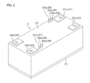
- FIG. 2 is a pictorial perspective view showing the exterior of the U-phase module 3 of FIG. 1 .
- the U-phase module 3 includes a heat dissipation plate 21, a substrate (not shown) that is fixed to the heat dissipation plate 21 and to which the MOSFETs 11 and 12, base ends of the terminals 31 to 39, etc., are fixed, and a case 22 that is fixed to one surface of the heat dissipation plate 21 and that contains the substrate.
- the case 22 is formed in a substantially rectangular shape when viewed planarly.
- the output terminal 33 of the module 3 forks in two directions within the case 22, and has two flat branch portions. Forward ends 33a and 33b of the branch portions pass through the upper surface of the case 22, and are exposed outwardly from the case 22.
- These forward ends 33a and 33b are disposed in a state along the upper surface of the case 22 at both sides of one end of the upper surface of the case 22, respectively.
- the first power supply terminal 31 and the second power supply terminal 32 of the module 3 are flat, and their forward ends 31a and 32a pass through the upper surface of the case 22, and are exposed outwardly from the case 22.
- These forward ends 31a and 32a are disposed in a state along the upper surface of the case 22 at both sides of the other end of the upper surface of the case 22, respectively.
- the gate terminal 34 which is one of the two gate terminals
- the source terminal 35 which is one of the two source terminals
- the source sense terminal 36 which is one of the two source sense terminals, of the module 3 are rod-shaped terminals, and their forward ends 34a, 35a, and 36a pass through the upper surface of the case 22, and protrude outwardly from the case 22.
- These forward ends 34a, 35a, and 36a are disposed adjacently to the forward end 31a of the first power supply terminal 31 in the upper surface of the case 22.
- the other gate terminal 37, the other source terminal 38, and the other source sense terminal 39 of the module 3 are rod-shaped terminals, and their forward ends 37a, 38a, and 39a pass through the upper surface of the case 22, and protrude outwardly from the case 22. These forward ends 37a, 38a, and 39a are disposed adjacently to the forward end 33b, which is one of the two forward ends, of the output terminal 33 in the upper surface of the case 22.
- the V-phase module 4 and the W-phase module 5 have the same exterior and the same structure as those of the U-phase module 3, and therefore a description of these exterior and structure is omitted.
- FIG. 3 is a plan view chiefly showing external electric wires connected to the power supply terminals 31, 32, 41, 42, 51, and 52 of the modules 2, 3, and 4 and showing snubber circuits connected thereto.
- Each of the modules 3, 4, and 5 is attached to a cooling plate 201.
- the output terminal 33 of the U-phase module 3 is connected to the U-phase field winding 8U of the electric motor 8 through the external electric wire 67.
- the output terminal 43 of the V-phase module 4 is connected to the V-phase field winding 8V of the electric motor 8 through the external electric wire 68.
- the output terminal 53 of the W-phase module 5 is connected to the W-phase field winding 8W of the electric motor 8 through the external electric wire 69.
- One end of a bus bar 61a is screwed to the first power supply terminal 31 of the U-phase module 3.
- the other end of the bus bar 61a is connected to the positive terminal of the power source 6 through a connection line 61b.
- the first external electric wire 61 of FIG. 1 consists of the bus bar 61a and the connection line 61b.
- One end of a bus bar 64a is screwed to the second power supply terminal 32 of the U-phase module 3.
- the other end of the bus bar 64a is connected to the negative terminal of the power source 6 through a connection line 64b.
- the fourth external electricwire 64 of FIG. 1 consists of the bus bar 64a and the connection line 64b.
- the smoothing capacitor 7 is connected to the power source 6 in parallel.
- bus bar 62 (corresponding to the second external electric wire 62 of FIG. 1 ) is screwed to the first power supply terminal 41 of the V-phase module 4.
- the other end of the bus bar 62 is connected to an intermediate part of the bus bar 61a.
- One end of a bus bar 65 (corresponding to the fifth external electric wire 65 of FIG. 1 ) is screwed to the second power supply terminal 42 of the V-phase module 4.
- the other end of the bus bar 65 is connected to an intermediate part of the bus bar 64a.
- One end of a bus bar 63 (corresponding to the third external electric wire 63 of FIG. 1 ) is screwed to the first power supply terminal 51 of the W-phase module 5.
- the other end of the bus bar 63 is connected to the intermediate part of the bus bar 61a.
- One end of a bus bar 66 (corresponding to the sixth external electric wire 66 of FIG. 1 ) is screwed to the second power supply terminal 52 of the W-phase module 5.
- the other end of the bus bar 66 is connected to the intermediate part of the bus bar 64a.
- a capacitor 91 is connected between a part of the bus bar 61a closer to the first power supply terminal 31 and a part of the bus bar 64a closer to the second power supply terminal 32.
- a capacitor 92 is connected between a part of the bus bar 62 closer to the first power supply terminal 41 and a part of the bus bar 65 closer to the second power supply terminal 42.
- a capacitor 93 is connected between a part of the bus bar 63 closer to the first power supply terminal 51 and a part of the bus bar 66 closer to the second power supply terminal 52.
- each of the capacitors 91, 92, and 93 is connected (to an A-to-C area S) between one end (position A) of each of the corresponding bus bars 61a, 62, and 63 closer to the first power supply terminals 31, 41, and 51 and a position (position C) located at a predetermined distance x in a direction receding from the first power supply terminals 31, 41, and 51 with respect to a position (position B) of each of the corresponding bus bars 61a, 62, and 63 nearest to an outer end of each of the first power supply terminals 31, 41, and 51.
- each of the capacitors 91, 92, and 93 is connected (to an A-to-C area S) between one end (position A) of each of the corresponding bus bars 64a, 65, and 66 closer to the second power supply terminals 32, 42, and 52 and a position (position C) located at a predetermined distance x in a direction receding from the second power supply terminals 32, 42, and 52 with respect to a position (position B) of each of the corresponding bus bars 64a, 65, and 66 nearest to an outer end of each of the second power supply terminals 32, 42, and 52.
- the predetermined distance x is set so that the inductance of the part from position B to position C in each of the bus bars 61a, 62, 63, 64a, 65, and 66 is 6.25 (nH) or less.
- This predetermination of the distance x makes it possible to reduce both the switching loss caused when a MOSFET is turned off and the surge voltage applied to this MOSFET as described later.
- the two bus bars 61a and 64a connected to the two power supply terminals 31 and 32 of the module 3 are disposed such that their intermediate parts coincide with each other in the up-down direction when viewed planarly so that their inductance components are offset.
- the two bus bars 62 and 65 connected to the two power supply terminals 41 and 42 of the module 4 are disposed such that their intermediate parts coincide with each other in the up-down direction when viewed planarly.
- the two bus bars 63 and 66 connected to the two power supply terminals 51 and 52 of the module 5 are disposed such that their intermediate parts coincide with each other in the up-down direction when viewed planarly.
- a load current flows back through a closed circuit that includes the output terminal 33, the seventh external electric wire 67, the U-phase field winding 8U and the V-phase field winding 8V of the electric motor 8, the eighth external electric wire 68, the output terminal 43, the connection metal member 77, the MOSFET 14, the connection metal member 78, the second power supply terminal 42, the fifth external electric wire 65, the interval part between a connection point with the fifth external electric wire 65 and the second output terminal 32 in the fourth external electric wire 64, the second output terminal 32, the connection metal member 74, the PN junction diode 12a, and the connection metal member 73.
- a surge voltage (Ls ⁇ di/dt) depending on the electric current rate of change (di/dt) of the drain current of the MOSFET 11 and depending on the predetermined parasitic inductance Ls of the circuit wiring is applied to the MOSFET 11.
- the inductance Lst that causes the generation of the surge voltage applied to the MOSFET 11 becomes equal to the sum of an inductance (part of L4a) between the connection point with the fifth wiring line 65 and the negative terminal of the power source 6 in the fourth external electric wire 64, an inductance (L1a + L1b) of the first external electric wire 61, inductances L11 and L12 of the connection metal members 71 and 72, an inductance (sum of L4b and part of L4a) of an interval part between the connection point with the fifth wiring line 65 and the second power supply terminal 32 in the fourth external electric wire 64, and inductances L13 and L14 of the connection metal members 73 and 74.
- the snubber circuits 91 to 93 are provided, and therefore energy stored in the inductance L4a of the interval part between the connection point A4 and the negative terminal of the power source 6 in the fourth external electric wire 64 and stored in the inductance L1a of the interval part between the positive terminal of the power source 6 and the connection point A1 in the first external electric wire 61 is absorbed by the capacitor 91.
- the inductance Lsn that causes the generation of the surge voltage applied to the MOSFET 11 becomes equal to the sum of the inductance L1b of the interval part between the connection point A1 and the first power supply terminal 31 in the first external electric wire 61, the inductances L11, L12, L13, and L14 of the connection metal members 71, 72, 73, and 74, and the inductance L4b of the interval part between the connection point A4 and the second power supply terminal 31 in the fourth external electric wire 64.
- the inductance Lsn that causes the generation of the surge voltage applied to the MOSFET 11 is made much smaller than the inductance Lst caused when the snubber circuits 91 to 93 are not provided. Therefore, the surge voltage applied to the MOSFET 11 is made much smaller than when the snubber circuits 91 to 93 are not provided.
- a load current flows back through a closed circuit that includes the first power supply terminal 31, the connection metal member 71, the MOSFET 11, the connection metal member 72, the output terminal 33, the seventh external electric wire 67, the U-phase field winding 8U and the V-phase field winding 8V of the electric motor 8, the eighth external electric wire 68, the output terminal 43, the connection metal member 76, the PN junction diode 13a, the connection metal member 75, the first power supply terminal 41, the second external electric wire 62, and an interval part between a connection point with the second external electric wire 62 and the first power supply terminal 31 in the first external electric wire 61.
- a surge voltage (Ls ⁇ di/dt) depending on the electric current rate of change (di/dt) of the drain current of the MOSFET 14 and depending on the predetermined parasitic inductance Ls of the circuit wiring is applied to the MOSFET 14.
- the inductance Lst that causes the generation of the surge voltage applied to the MOSFET 14 becomes equal to the sum of an inductance (part of L1a) between the positive terminal of the power source 6 and a connection point with the second wiring line 62 in the first external electric wire 61, inductances L17 and L18 of the connection metal members 77 and 78, an inductance (L5a + L5b) of the fifth external electric wire 65, an inductance of an interval part (part of L4a) between a connection point with the fifth external electric wire 65 and the negative terminal of the power source 6 in the fourth external electric wire 64, an inductance (L2a+L2b) of the second external electric wire member 62, and inductances L15 and L16 of the connection metal members 75 and 76.
- the snubber circuits 91 to 93 are provided, and therefore energy stored in the inductance of an interval part (part of L1a) between the positive terminal of the power source 6 and a connection point with the second wiring line 62 in the first external electric wire 61, the inductance L5a of an interval part between the connection point A5 and a connection point with the fourth external electric wire 64 in the fifth external electric wire 65, the inductance of an interval part (part of L4a) between a connection point with the fifth external electric wire 65 and the negative terminal of the power source 6 in the fourth external electric wire 64, and the inductance L2a of an interval part between a connection point with the first external electric wire 61 and the connection point A2 in the second external electric wire 62 is absorbed by the capacitor 92.
- the inductance Lsn that causes the generation of the surge voltage applied to the MOSFET 14 becomes equal to the sumof the inductance L2b of an interval part between the connection point A2 and the first power supply terminal 41 in the second external electric wire 62, the inductances L15, L16, L17, and L18 of the connection metal members 75, 76, 77, and 78, and the inductance L5b of an interval part between the second power supply terminal 42 and the connection point A5 in the fifth external electric wire 65.
- the inductance Lsn that causes the generation of the surge voltage applied to the MOSFET 14 is made much smaller than the inductance Lst caused when the snubber circuits 91 to 93 are not provided. Therefore, the surge voltage applied to the MOSFET 14 is made much smaller than when the snubber circuits 91 to 93 are not provided.
- a load current flows in a direction from the fourth external electric wire 64 toward the first external electric wire 61 through the fourth external electric wire 64, the second power supply terminal 32, the connection metal member 74, the PN junction diode 12a, the connection metal member 73, the output terminal 33, the seventh external electric wire 67, the U-phase field winding 8U and the V-phase field winding 8V of the electric motor 8, the eighth external electric wire 68, the output terminal 43, the connection metal member 76, the PN junction diode 13a, the connection metal member 75, the first power supply terminal 41, the second external electric wire 62, and an interval part between a connection point with the second external electric wire 62 and the positive terminal of the power source 6 in the first external electric wire 61.
- the inductance Lsn that causes the generation of the surge voltage applied to the MOSFET 11 becomes equal to the sum of the inductance L1b, the inductances L11 to L14 (internal inductances in the U-phase module 3), and the inductance L4b.
- the inductance Lsn that causes the generation of the surge voltage applied to the MOSFET 14 becomes equal to the sum of the inductance L2b, the inductances L15 to L18 (internal inductances in the V-phase module 4), and the inductance L5b.
- the inductance Lsn (hereinafter, referred to as the inductance "Lsn U " when necessary) that causes the generation of the surge voltage applied to this one becomes equal to the sum of the inductance L1b, the inductances L11 to L14 (internal inductances in the U-phase module 3), and the inductance L4b.
- the inductanceLsn (hereinafter, referred to as the inductance "Lsn V " when necessary) that causes the generation of the surge voltage applied to this one becomes equal to the sum of the inductance L2b, the inductances L15 to L18 (internal inductances in the V-phase module 4), and the inductance L5b.
- the inductance Lsn (hereinafter, referred to as the inductance "Lsn W " when necessary) that causes the generation of the surge voltage applied to this one becomes equal to the sum of the inductance L3b, the inductances L19 to L22 (internal inductances in the W-phase module 5), and the inductance L6b.
- the inductances Lsn U , Lsn V , and Lsn W are substantially equal to each other.
- the inductances Lsn U , Lsn V , and Lsn W are 40 (nH) or less as described later.
- the rate of change di/dt of the drain current of the MOSFET becomes greater(i.e., the falling of "di" becomes earlier) in proportion to a reduction of the inductance Lsn that causes the generation of the surge voltage applied to the MOSFET (excluding inductances by which energy stored by the snubber circuits 91 to 93 is absorbed), and therefore the switching loss caused when the MOSFET is turned off becomes smaller. Therefore, the switching loss caused when the MOSFET is turned off can be reduced by reducing the inductance Lsn that causes the generation of a surge voltage, and the surge voltage can be reduced.
- one end of each of the capacitors 91, 92, and 93 is connected to the position of each of the external electric wires 61, 62, and 63 closer to the first power supply terminals 31, 41, and 51, respectively, and therefore the inductances L1b, L2b, and L3b of external electric wire parts between respective ends of the snubber circuits 91, 92, and 93 and the first power supply terminals 31, 41, and 51 can be reduced.
- each of the capacitors 91, 92, and 93 is connected to the position of each of the external electric wires 64, 65, and 66 closer to the second power supply terminals 32, 42, and 52, respectively, and therefore the inductances L4b, L5b, and L6b of external electric wire parts between the respective other ends of the snubber circuits 91, 92, and 93 and the second power supply terminals 32, 42, and 52 can be reduced.
- a plurality of samples "a” to “g” having mutually different inductances Lsn were prepared. More specifically, a plurality of samples a to g having mutually different inductances Lsn were prepared by changing the distance from one end of each of the bus bars 61a, 64a, 62, 65, 63, and 66 closer to the power supply terminals 31, 32, 41, 42, 51, and 52 to the connection positions of the capacitors 91 to 93.
- each of the bus bars 61a, 64a, 62, 65, 63, and 66 closer to the power supply terminals 31, 32, 41, 42, 51, and 52 to the connection positions of the capacitors 91 to 93 is set so as to become longer in order of samples a, b, c, d, e, f, and g, sample "a" having the shortest distance.
- both ends of each of the capacitors 91 to 93 are connected (to an A-to-B area) between one end (position A) of each of the corresponding bus bars 61a, 64a, 62, 65, 63, and 66 closer to the power supply terminals 31, 32, 41, 42, 51, and 52 and the position (position B) corresponding to the outer end of each of the power supply terminals 31, 32, 41, 42, 51, and 52.
- both ends of each of the capacitors 91 to 93 are connected to a position fixed more apart from each of the power supply terminals 31, 32, 41, 42, 51, and 52 than the position (position B) corresponding to the outer end of each of the power supply terminals 31, 32, 41, 42, 51, and 52 in the corresponding bus bars 61a, 64a, 62, 65, 63, and 66.
- the inductances L1b, L4b, L2b, L5b, L3b, and L6b become greater in order of samples a, b, c, d, e, f, and g. Therefore, the inductance Lsn that causes the generation of a surge voltage applied to a MOSFET that has been turned off becomes greater in order of samples a, b, c, d, e, f, and g.
- the gate resistance was adjusted so that the MOSFET 11 is turned off from a state in which the MOSFET 11 and the MOSFET 14 have been turned on and so that the surge voltage (Lsn ⁇ di/dt) applied to the MOSFET 11 reaches a predetermined value when the MOSFET 11 is turned off.
- the MOSFET 11 was turned off from a state in which the MOSFET 11 and the MOSFET 14 have been turned on, and then the switching loss (mJ) at the turn-off time of the MOSFET 11 and the rate of change di/dt (A/ns) of the drain current of the MOSFET 11 were measured.
- the power-supply voltage V was set at 600(V), and the power source electric current I was set at 100(A). Additionally, the gate resistance was adjusted so that the surge voltage reaches 156(V).
- Table 1 and FIG. 4 show measurement results.
- the black triangle ( ⁇ ) represents switching loss
- the white triangle ( ⁇ ) represents di/dt.
- the inductances L1b and L4b are included in the inductance Lsn U , and therefore what is needed is to allow the amount of increase in L1b and in L4b to reach 6.25(nH), which is half of 12.5(nH), or less with respect to sample "a.”
- the inductances L1b and L4b are small in sample “a,” and the inductance (L11+L12+L13+L14) in the module 3 is substantially equal to the inductance Lsn with respect to sample “a.” If so, when the inductance in the module 3 is about 27.5 (nH), what is needed for setting the inductance Lsn U at about 40(nH) or less will be to set x, which determines a preferred connection range (A-to-C area S of FIG. 3 ) of the capacitor 91 with respect to the bus bars 61a and 64a, at 6.25(nH) or less.
- the inductance Lsn V and the inductance Lsn W are set at about 40(nH) or less. Therefore, what is needed is to set both x, which determines a preferred connection range (A-to-C area S of FIG. 3 ) of the capacitor 92 with respect to the bus bars 62 and 65, and x, which determines a preferred connection range (A-to-C area S of FIG. 3 ) of the capacitor 93 with respect to the bus bars 63 and 66, at 6.25(nH) or less.
- each of the MOSFETs 11, 12, 13, and 14 may be a Si device that uses Si (silicon) as a semiconductor material although each is a SiC device in the aforementioned embodiment.
- the present invention can be applied also to electronic circuits other than a three-phase inverter circuit, such as an H bridge circuit although the present invention is applied to the three-phase inverter circuit as described in the aforementioned embodiment.
Landscapes
- Engineering & Computer Science (AREA)
- Power Engineering (AREA)
- Inverter Devices (AREA)
Description
- The present invention relates to an electronic circuit, such as a three-phase inverter circuit or an H bridge circuit.
- A MOSFET (Metal-Oxide-Semiconductor Field Effect Transistor), such as a DMOSFET (Double Diffused MOSFET), or an IGBT (Insulated Gate Bipolar Transistor) is used as a switching element of an electronic circuit, such as a three-phase inverter circuit or an H bridge circuit. A gate drive signal is supplied to a gate terminal of the MOSFET or of the IGBT through a gate resistor.
-
FIG. 5 is a graph showing a relationship among gate resistance, switching loss (DMOS Eoff) caused when a DMOSFET is turned off, and surge voltage and showing a relationship among gate resistance, switching loss (IGBT Eoff) caused when an IGBT is turned off, and surge voltage. - In the IGBT, the gate resistance dependency of switching loss at the turn-off time is low. Additionally, in the IGBT, the amount of increase of the surge voltage is small with respect to an increase of the gate resistance. On the other hand, in the DMOSFET, the switching loss at the turn-off time can be made much smaller by reducing the gate resistance than in the IGBT. However, in the DMOSFET, if the gate resistance is reduced, the rate of change di/dt of a drain current at the turn-off time will become great, and therefore a great surge voltage will be generated.
- As shown in
FIG. 4 ,Patent Literature 1 discloses an arrangement in which, in a three-phase inverter circuit including six IGBTs, a snubber circuit is connected between a single DC input terminal P to which a collector of high-side IGBTs equivalent to three phases is connected and a single DC input terminal N to which an emitter of low-side IGBTs equivalent to three phases is connected, in order to restrain a surge voltage. - PTL 1: Japanese Unexamined Patent Publication No.
H7-122708 - An object of the present invention is to provide an electronic circuit capable of reducing the switching loss and capable of reducing the surge voltage when a MOSFET is turned off.
- The electronic circuit of the present invention is an electronic circuit having a plurality of series circuits each of which has two MOSFETs connected in series in which a first power supply terminal is connected to one end of each of the series circuits and in which a second power supply terminal is connected to an opposite end of each of the series circuits, and the electronic circuit is composed of a first bus bar one end of which is connected to each of the first power supply terminals and that forms a part of an external electric wire to connect the first power supply terminal to one terminal of a power source, a second bus bar one end of which is connected to each of the second power supply terminals and that forms a part of an external electric wire to connect the second power supply terminal to an opposite terminal of the power source, and a snubber circuit that is provided in each of the series circuits and that is connected between the first bus bar connected to the series circuit through the first power supply terminal and the second bus bar connected to the series circuit through the second power supply terminal. In the electronic circuit, one end of each of the snubber circuits is connected to a part of the corresponding first bus bar closer to the first power supply terminal, whereas an opposite end of each of the snubber circuits is connected to a part of the corresponding second bus bar closer to the second power supply terminal.
- The present invention includes a snubber circuit that is provided in each series circuit and that is connected between the first bus bar connected to the series circuit through the first power supply terminal and the second bus bar connected to the series circuit through the second power supply terminal, and therefore the surge voltage applied to a MOSFET when the MOSFET is turned off can be reduced.
- Additionally, one end of each snubber circuit is connected to a part of the corresponding first bus bar closer to the first power supply terminal, and therefore the inductance of an interval part between the connection position of the snubber circuit and the first power supply terminal in the first bus bar can be reduced. Additionally, an opposite end of each snubber circuit is connected to a part of the corresponding second bus bar closer to the second power supply terminal, and therefore the inductance of an interval part between the connection position of the snubber circuit and the second power supply terminal in the second bus bar can be reduced. As a result, when the MOSFET is turned off, an inductance (excluding inductances by which energy stored by the snubber circuits is absorbed) that causes the generation of the surge voltage applied to the MOSFET can be reduced.
- When the connection position of each snubber circuit with respect to a bus bar is changed and when gate resistance is changed so that the surge voltage applied to a MOSFET that has been turned off becomes constant, switching loss caused when the MOSFET is turned off becomes smaller in proportion to a reduction of the inductance that causes the generation of the surge voltage applied to the MOSFET. In the present invention, the inductance can be reduced, and therefore the switching loss at the turn-off time of the MOSFET can be reduced, and the surge voltage can be reduced.
- In one embodiment of the present invention, in a combination of an arbitrary one of the series circuits, the first and second power supply terminals connected to both ends of the arbitrary one, the first and second bus bars connected thereto, and the snubber circuit connected therebetween, a sum of an inductance of an interval part between a connection point with one end of the snubber circuit and the first power supply terminal in the first bus bar, an inductance of an interval part between a connection point with an opposite end of the snubber circuit and the second power supply terminal in the second bus bar, and an inductance of the series circuit between the first power supply terminal and the second power supply terminal is 40 nH or less.
- In this arrangement, when either one of the two MOSFETs included in the series circuit in the combination is turned off, the inductance that causes the generation of the surge voltage applied to the MOSFET that has been turned off can be reduced to be 40 nH or less, and therefore the switching loss at the turn-off time of the MOSFET can be reduced, and the surge voltage can be reduced.
- In one embodiment of the present invention, one end of the snubber circuit is connected between one end of the first bus bar closer to the first power supply terminal and a second position of the first bus bar located at a first predetermined distance with respect to a first position of the first bus bar nearest to an outer end of the first power supply terminal in a direction receding from the first power supply terminal. The first predetermined distance is set so that an inductance of a part of the first bus bar from the first position to the second position becomes equal to 6.25 nH or less. An opposite end of the snubber circuit is connected between one end of the second bus bar closer to the second power supply terminal and a fourth position located at a second predetermined distance with respect to a third position nearest to an outer end of the second power supply terminal in a direction receding from the second power supply terminal. The second predetermined distance is set so that an inductance of a part of the second bus bar from the third position to the fourth position becomes equal to 6.25 nH or less.
- In this arrangement, the inductance that causes the generation of the surge voltage applied to the MOSFET that has been turned off can be reduced, and therefore the switching loss at the turn-off time of the MOSFET can be reduced, and the surge voltage can be reduced.
- In one embodiment of the present invention, each of the MOSFETs is a SiC-MOSFETmade of a semiconductormaterial composed chiefly of SiC.
-
- [
FIG. 1] FIG. 1 is an electric circuit diagram showing a three-phase inverter circuit according to an embodiment of the present invention. - [
FIG. 2] FIG. 2 is a pictorial perspective view showing the exterior of a U-phase module, which is used for a U phase, ofFIG. 1 . - [
FIG. 3] FIG. 3 is a plan view chiefly showing external electric wires connected to power supply terminals of modules and snubber circuits connected thereto. - [
FIG. 4] FIG. 4 is a graph showing measurement results of the switching loss (mJ) with respect to samples "a" to "g" when a MOSFET is turned off and the rate of change di/dt (A/ns) of a drain current. - [
FIG. 5] FIG. 5 is a graph showing a relationship among gate resistance, switching loss caused when a DMOSFET is turned off, and surge voltage and showing a relationship among gate resistance, switching loss caused when an IGBT is turned off, and surge voltage. - An embodiment of the present invention will be hereinafter described in detail with reference to the accompanying drawings.
-
FIG. 1 is an electric circuit diagram showing a three-phase inverter circuit 1 according to an embodiment of the present invention. - This three-
phase inverter circuit 1 is a circuit to drive a three-phase brushless motor 8 (hereinafter, referred to as an "electric motor"). The electric motor 8 is composed of a stator that has aU-phase field coil 8U, a V-phase field coil 8V, and a W-phase field coil 8W and a rotor to which a permanent magnet is fixed. - The three-
phase inverter circuit 1 includes aU-phase module 3 that is used for a U phase, a V-phase module 4 that is used for a V phase, and a W-phase module 5 that is used for a W phase. TheU-phase module 3 is composed of a first power supply terminal (P terminal) 31, a second power supply terminal (N terminal) 32, an output terminal (OUT terminal) 33, twogate terminals source terminals source sense terminals - The V-
phase module 4 is composed of a first power supply terminal (P terminal) 41, a second power supply terminal (N terminal) 42, an output terminal (OUT terminal) 43, twogate terminals source terminals source sense terminals phase module 5 is composed of a first power supply terminal (P terminal) 51, a second power supply terminal (N terminal) 52, an output terminal (OUT terminal) 53, twogate terminals source terminals 55 and 58, and twosource sense terminals - Each of the first
power supply terminals modules power supply terminal 31 of theU-phase module 3 is connected to the positive terminal of thepower source 6 through a first externalelectric wire 61. The firstpower supply terminal 41 of the V-phase module 4 is connected to an intermediate part of the first externalelectric wire 61 through a second externalelectric wire 62. The firstpower supply terminal 51 of the W-phase module 5 is connected to the intermediate part of the first externalelectric wire 61 through a third externalelectric wire 63. - Each of the second
power supply terminals modules power source 6 through an external electric wire. More specifically, the secondpower supply terminal 32 of theU-phase module 3 is connected to the negative terminal of thepower source 6 through a fourth externalelectric wire 64. The secondpower supply terminal 42 of the V-phase module 4 is connected to an intermediate part of the fourth externalelectric wire 64 through a fifth externalelectric wire 65. The secondpower supply terminal 52 of the W-phase module 5 is connected to the intermediate part of the fourth externalelectric wire 64 through a sixth externalelectric wire 66. An inductance parasitizes each of the externalelectric wires 61 to 66. - A
smoothing capacitor 7 is connected to thepower source 6 in parallel. Theoutput terminals modules electric wires gate terminals source sense terminals modules gate terminals modules - The
U-phase module 3 includes a high-side first MOSFET 11 and a low-side second MOSFET 12 connected in series thereto. TheMOSFETs 11 and 12 have a built-in first PN junction diode (body diode) 11a and a built-in secondPN junction diode 12a, respectively. Anodes of thePN junction diodes MOSFETs 11 and 12, respectively, and cathodes thereof are electrically connected to corresponding drains of theMOSFETs 11 and 12, respectively. TheMOSFETs 11 and 12 are provided with current detectingportions - The drain of the first MOSFET 11 is connected to the first
power supply terminal 31 of theU-phase module 3 through aconnection metal member 71. The source of the first MOSFET 11 is connected to theoutput terminal 33 of theU-phase module 3 through aconnection metal member 72. Inductances L11 and L12 parasitize theconnection metal members source terminal 35 of theU-phase module 3. The current detectingportion 11b is connected to thesource sense terminal 36 of theU-phase module 3. The gate of the first MOSFET 11 is connected to thegate terminal 34 of theU-phase module 3. - The drain of the
second MOSFET 12 is connected to theoutput terminal 33 of theU-phase module 3 through aconnection metal member 73. The source of thesecond MOSFET 12 is connected to the secondpower supply terminal 32 of theU-phase module 3 through a connection metal member 74. Inductances L13 and L14 parasitize theconnection metal members 73 and 74, respectively. The source of thesecond MOSFET 12 is further connected to thesource terminal 38 of theU-phase module 3. The current detectingportion 12b is connected to thesource sense terminal 39 of theU-phase module 3. The gate of thesecond MOSFET 12 is connected to thegate terminal 37 of theU-phase module 3. - The V-
phase module 4 includes a high-sidethird MOSFET 13 and a low-sidefourth MOSFET 14 connected in series thereto. TheMOSFETs PN junction diodes MOSFETs MOSFETs MOSFETs portions - The drain of the
third MOSFET 13 is connected to the firstpower supply terminal 41 of the V-phase module 4 through aconnection metal member 75. The source of thethird MOSFET 13 is connected to theoutput terminal 43 of the V-phase module 4 through aconnection metal member 76. Inductances L15 and L16 parasitize theconnection metal members third MOSFET 13 is further connected to thesource terminal 45 of the V-phase module 4. The current detectingportion 13b is connected to thesource sense terminal 46 of the V-phase module 4. The gate of thethird MOSFET 13 is connected to thegate terminal 44 of the V-phase module 4. - The drain of the
fourth MOSFET 14 is connected to theoutput terminal 43 of the V-phase module 4 through aconnection metal member 77. The source of thefourth MOSFET 14 is connected to the secondpower supply terminal 42 of the V-phase module 4 through aconnection metal member 78. Inductances L17 and L18 parasitize theconnection metal members fourth MOSFET 14 is further connected to thesource terminal 48 of the V-phase module 4. The current detectingportion 14b is connected to thesource sense terminal 49 of the V-phase module 4. The gate of thefourth MOSFET 14 is connected to thegate terminal 47 of the V-phase module 4. - The W-
phase module 5 includes a high-sidefifth MOSFET 15 and a low-sidesixth MOSFET 16 connected in series thereto. TheMOSFETs PN junction diodes MOSFETs MOSFETs MOSFETs portions - The drain of the
fifth MOSFET 15 is connected to the firstpower supply terminal 51 of the W-phase module 5 through aconnection metal member 79. The source of thefifth MOSFET 15 is connected to theoutput terminal 53 of the W-phase module 5 through aconnection metal member 80. Inductances L19 and L20 parasitize theconnection metal members fifth MOSFET 15 is further connected to thesource terminal 55 of the W-phase module 5. The current detectingportion 15b is connected to thesource sense terminal 56 of the W-phase module 5. The gate of thefifth MOSFET 15 is connected to thegate terminal 54 of the W-phase module 5. - The drain of the
sixth MOSFET 16 is connected to theoutput terminal 53 of the W-phase module 5 through aconnection metal member 81. The source of thesixth MOSFET 16 is connected to the secondpower supply terminal 52 of the W-phase module 5 through a connection metal member 82. Inductances L21 and L22 parasitize theconnection metal members 81 and 82, respectively. The source of thesixth MOSFET 16 is further connected to the source terminal 58 of the W-phase module 5. The current detectingportion 16b is connected to thesource sense terminal 59 of the W-phase module 5. The gate of thesixth MOSFET 16 is connected to thegate terminal 57 of the W-phase module 5. - For example, each of the first to sixth MOSFETs 11 to 16 is a SiC-MOSFET, such as a SiC-DMOSFET, that uses SiC (silicon carbide) as a semiconductor material, which is one example of a compound semiconductor.
- A snubber circuit composed of a
capacitor 91 is connected between a part of the first externalelectric wire 61 closer to the firstpower supply terminal 31 of theU-phase module 3 and a part of the fourth externalelectric wire 64 closer to the secondpower supply terminal 32 of theU-phase module 3. - Let the connection point between the first external
electric wire 61 and thecapacitor 91 be a connection point A1. An inductance L1a parasitizes an interval part between a positive terminal of thepower source 6 and the connection point A1 in the first externalelectric wire 61, and an inductance L1b parasitizes an interval part between the connection point A1 and the firstpower supply terminal 31 in the first externalelectric wire 61. Let the connection point between the fourth externalelectric wire 64 and thecapacitor 91 be a connection point A4. An inductance L4a parasitizes an interval part between a negative terminal of thepower source 6 and the connection point A4 in the fourth externalelectric wire 64, and an inductance L4b parasitizes an interval part between the connection point A4 and the secondpower supply terminal 32 in the fourth externalelectric wire 64. - A snubber circuit composed of a
capacitor 92 is connected between a part of the second externalelectric wire 62 closer to the firstpower supply terminal 41 of the V-phase module 4 and a part of the fifth externalelectric wire 65 closer to the secondpower supply terminal 42 of the V-phase module 4. - Let the connection point between the second external
electric wire 62 and thecapacitor 92 be a connection point A2. An inductance L2b parasitizes an interval part between the connection point A2 and the firstpower supply terminal 41 in the second externalelectric wire 62, and an inductance L2a parasitizes the remaining part. Let the connection point between the fifth externalelectric wire 65 and thecapacitor 92 be a connection point A5. An inductance L5b parasitizes an interval part between the connection point A5 and the secondpower supply terminal 42 in the fifth externalelectric wire 65, and an inductance L5a parasitizes the remaining part. - A snubber circuit composed of a
capacitor 93 is connected between a part of the third externalelectric wire 63 closer to the firstpower supply terminal 51 of the W-phase module 5 and a part of the sixth externalelectric wire 66 closer to the secondpower supply terminal 52 of the W-phase module 5. - Let the connection point between the third external
electric wire 63 and thecapacitor 93 be a connection point A3. An inductance L3b parasitizes an interval part between the connection point A3 and the firstpower supply terminal 51 in the third externalelectric wire 63, and an inductance L3a parasitizes the remaining part. Let the connection point between the sixth externalelectric wire 66 and thecapacitor 93 be a connection point A6. An inductance L6b parasitizes an interval part between the connection point A6 and the secondpower supply terminal 52 in the sixth externalelectric wire 66, and an inductance L6a parasitizes the remaining part. The capacitors (snubber circuits) 91 to 93 are provided to restrain the surge voltage. -
FIG. 2 is a pictorial perspective view showing the exterior of theU-phase module 3 ofFIG. 1 . - The
U-phase module 3 includes aheat dissipation plate 21, a substrate (not shown) that is fixed to theheat dissipation plate 21 and to which theMOSFETs 11 and 12, base ends of theterminals 31 to 39, etc., are fixed, and acase 22 that is fixed to one surface of theheat dissipation plate 21 and that contains the substrate. Thecase 22 is formed in a substantially rectangular shape when viewed planarly. Theoutput terminal 33 of themodule 3 forks in two directions within thecase 22, and has two flat branch portions. Forward ends 33a and 33b of the branch portions pass through the upper surface of thecase 22, and are exposed outwardly from thecase 22. These forward ends 33a and 33b are disposed in a state along the upper surface of thecase 22 at both sides of one end of the upper surface of thecase 22, respectively. The firstpower supply terminal 31 and the secondpower supply terminal 32 of themodule 3 are flat, and their forward ends 31a and 32a pass through the upper surface of thecase 22, and are exposed outwardly from thecase 22. These forward ends 31a and 32a are disposed in a state along the upper surface of thecase 22 at both sides of the other end of the upper surface of thecase 22, respectively. - The
gate terminal 34, which is one of the two gate terminals, thesource terminal 35, which is one of the two source terminals, and thesource sense terminal 36, which is one of the two source sense terminals, of themodule 3 are rod-shaped terminals, and their forward ends 34a, 35a, and 36a pass through the upper surface of thecase 22, and protrude outwardly from thecase 22. These forward ends 34a, 35a, and 36a are disposed adjacently to theforward end 31a of the firstpower supply terminal 31 in the upper surface of thecase 22. Theother gate terminal 37, theother source terminal 38, and the othersource sense terminal 39 of themodule 3 are rod-shaped terminals, and their forward ends 37a, 38a, and 39a pass through the upper surface of thecase 22, and protrude outwardly from thecase 22. These forward ends 37a, 38a, and 39a are disposed adjacently to theforward end 33b, which is one of the two forward ends, of theoutput terminal 33 in the upper surface of thecase 22. - The V-
phase module 4 and the W-phase module 5 have the same exterior and the same structure as those of theU-phase module 3, and therefore a description of these exterior and structure is omitted. -
FIG. 3 is a plan view chiefly showing external electric wires connected to thepower supply terminals modules - Each of the
modules cooling plate 201. Theoutput terminal 33 of theU-phase module 3 is connected to the U-phase field winding 8U of the electric motor 8 through the externalelectric wire 67. Theoutput terminal 43 of the V-phase module 4 is connected to the V-phase field winding 8V of the electric motor 8 through the externalelectric wire 68. Theoutput terminal 53 of the W-phase module 5 is connected to the W-phase field winding 8W of the electric motor 8 through the externalelectric wire 69. - One end of a
bus bar 61a is screwed to the firstpower supply terminal 31 of theU-phase module 3. The other end of thebus bar 61a is connected to the positive terminal of thepower source 6 through aconnection line 61b. The first externalelectric wire 61 ofFIG. 1 consists of thebus bar 61a and theconnection line 61b. One end of abus bar 64a is screwed to the secondpower supply terminal 32 of theU-phase module 3. The other end of thebus bar 64a is connected to the negative terminal of thepower source 6 through aconnection line 64b. The fourthexternal electricwire 64 ofFIG. 1 consists of thebus bar 64a and theconnection line 64b. The smoothingcapacitor 7 is connected to thepower source 6 in parallel. - One end of a bus bar 62 (corresponding to the second external
electric wire 62 ofFIG. 1 ) is screwed to the firstpower supply terminal 41 of the V-phase module 4. The other end of thebus bar 62 is connected to an intermediate part of thebus bar 61a. One end of a bus bar 65 (corresponding to the fifth externalelectric wire 65 ofFIG. 1 ) is screwed to the secondpower supply terminal 42 of the V-phase module 4. The other end of thebus bar 65 is connected to an intermediate part of thebus bar 64a. - One end of a bus bar 63 (corresponding to the third external
electric wire 63 ofFIG. 1 ) is screwed to the firstpower supply terminal 51 of the W-phase module 5. The other end of thebus bar 63 is connected to the intermediate part of thebus bar 61a. One end of a bus bar 66 (corresponding to the sixth externalelectric wire 66 ofFIG. 1 ) is screwed to the secondpower supply terminal 52 of the W-phase module 5. The other end of thebus bar 66 is connected to the intermediate part of thebus bar 64a. - A
capacitor 91 is connected between a part of thebus bar 61a closer to the firstpower supply terminal 31 and a part of thebus bar 64a closer to the secondpower supply terminal 32. Acapacitor 92 is connected between a part of thebus bar 62 closer to the firstpower supply terminal 41 and a part of thebus bar 65 closer to the secondpower supply terminal 42. Acapacitor 93 is connected between a part of thebus bar 63 closer to the firstpower supply terminal 51 and a part of thebus bar 66 closer to the secondpower supply terminal 52. - Preferably, one end of each of the
capacitors bus bars power supply terminals power supply terminals bus bars power supply terminals - Likewise, preferably, the other end of each of the
capacitors bus bars power supply terminals power supply terminals bus bars power supply terminals - Preferably, the predetermined distance x is set so that the inductance of the part from position B to position C in each of the
bus bars - Preferably, the two
bus bars power supply terminals module 3 are disposed such that their intermediate parts coincide with each other in the up-down direction when viewed planarly so that their inductance components are offset. Likewise, preferably, the twobus bars power supply terminals module 4 are disposed such that their intermediate parts coincide with each other in the up-down direction when viewed planarly. Likewise, preferably, the twobus bars power supply terminals module 5 are disposed such that their intermediate parts coincide with each other in the up-down direction when viewed planarly. - Referring again to
FIG. 1 , for example, when the high-side MOSFET 11 in theU-phase module 3 and the low-side MOSFET 14 in the V-phase module 4 are turned on among the MOSFETs 11 to 16, an electric current flows from the positive terminal of thepower source 6 to the negative terminal of thepower source 6 through the first externalelectric wire 61, the firstpower supply terminal 31, theconnection metal member 71, the MOSFET 11, theconnection metal member 72, theoutput terminal 33, the seventh externalelectric wire 67, the U-phase field winding 8U and the V-phase field winding 8V of the electric motor 8, the eighth externalelectric wire 68, theoutput terminal 43, theconnection metal member 77, theMOSFET 14, theconnection metal member 78, the secondpower supply terminal 42, the fifth externalelectric wire 65, and the fourth externalelectric wire 64. - When the high-side MOSFET 11 in the
U-phase module 3 is turned off from this state, a load current flows back through a closed circuit that includes theoutput terminal 33, the seventh externalelectric wire 67, the U-phase field winding 8U and the V-phase field winding 8V of the electric motor 8, the eighth externalelectric wire 68, theoutput terminal 43, theconnection metal member 77, theMOSFET 14, theconnection metal member 78, the secondpower supply terminal 42, the fifth externalelectric wire 65, the interval part between a connection point with the fifth externalelectric wire 65 and thesecond output terminal 32 in the fourth externalelectric wire 64, thesecond output terminal 32, the connection metal member 74, thePN junction diode 12a, and theconnection metal member 73. - In this example, a surge voltage (Ls·di/dt) depending on the electric current rate of change (di/dt) of the drain current of the MOSFET 11 and depending on the predetermined parasitic inductance Ls of the circuit wiring is applied to the MOSFET 11.
- If the
snubber circuits 91 to 93 are not provided, the inductance Lst that causes the generation of the surge voltage applied to the MOSFET 11 becomes equal to the sum of an inductance (part of L4a) between the connection point with thefifth wiring line 65 and the negative terminal of thepower source 6 in the fourth externalelectric wire 64, an inductance (L1a + L1b) of the first externalelectric wire 61, inductances L11 and L12 of theconnection metal members fifth wiring line 65 and the secondpower supply terminal 32 in the fourth externalelectric wire 64, and inductances L13 and L14 of theconnection metal members 73 and 74. - In the present embodiment, the
snubber circuits 91 to 93 are provided, and therefore energy stored in the inductance L4a of the interval part between the connection point A4 and the negative terminal of thepower source 6 in the fourth externalelectric wire 64 and stored in the inductance L1a of the interval part between the positive terminal of thepower source 6 and the connection point A1 in the first externalelectric wire 61 is absorbed by thecapacitor 91. As a result, the inductance Lsn that causes the generation of the surge voltage applied to the MOSFET 11 becomes equal to the sum of the inductance L1b of the interval part between the connection point A1 and the firstpower supply terminal 31 in the first externalelectric wire 61, the inductances L11, L12, L13, and L14 of theconnection metal members power supply terminal 31 in the fourth externalelectric wire 64. In other words, the inductance Lsn that causes the generation of the surge voltage applied to the MOSFET 11 is made much smaller than the inductance Lst caused when thesnubber circuits 91 to 93 are not provided. Therefore, the surge voltage applied to the MOSFET 11 is made much smaller than when thesnubber circuits 91 to 93 are not provided. - For example, when the low-
side MOSFET 14 in the V-phase module 4 is turned off from a state in which the MOSFET 11 and theMOSFET 14 have been turned on, a load current flows back through a closed circuit that includes the firstpower supply terminal 31, theconnection metal member 71, the MOSFET 11, theconnection metal member 72, theoutput terminal 33, the seventh externalelectric wire 67, the U-phase field winding 8U and the V-phase field winding 8V of the electric motor 8, the eighth externalelectric wire 68, theoutput terminal 43, theconnection metal member 76, thePN junction diode 13a, theconnection metal member 75, the firstpower supply terminal 41, the second externalelectric wire 62, and an interval part between a connection point with the second externalelectric wire 62 and the firstpower supply terminal 31 in the first externalelectric wire 61. - In this example, a surge voltage (Ls·di/dt) depending on the electric current rate of change (di/dt) of the drain current of the
MOSFET 14 and depending on the predetermined parasitic inductance Ls of the circuit wiring is applied to theMOSFET 14. - If the
snubber circuits 91 to 93 are not provided, the inductance Lst that causes the generation of the surge voltage applied to theMOSFET 14 becomes equal to the sum of an inductance (part of L1a) between the positive terminal of thepower source 6 and a connection point with thesecond wiring line 62 in the first externalelectric wire 61, inductances L17 and L18 of theconnection metal members electric wire 65, an inductance of an interval part (part of L4a) between a connection point with the fifth externalelectric wire 65 and the negative terminal of thepower source 6 in the fourth externalelectric wire 64, an inductance (L2a+L2b) of the second externalelectric wire member 62, and inductances L15 and L16 of theconnection metal members - In the present embodiment, the
snubber circuits 91 to 93 are provided, and therefore energy stored in the inductance of an interval part (part of L1a) between the positive terminal of thepower source 6 and a connection point with thesecond wiring line 62 in the first externalelectric wire 61, the inductance L5a of an interval part between the connection point A5 and a connection point with the fourth externalelectric wire 64 in the fifth externalelectric wire 65, the inductance of an interval part (part of L4a) between a connection point with the fifth externalelectric wire 65 and the negative terminal of thepower source 6 in the fourth externalelectric wire 64, and the inductance L2a of an interval part between a connection point with the first externalelectric wire 61 and the connection point A2 in the second externalelectric wire 62 is absorbed by thecapacitor 92. As a result, the inductance Lsn that causes the generation of the surge voltage applied to theMOSFET 14 becomes equal to the sumof the inductance L2b of an interval part between the connection point A2 and the firstpower supply terminal 41 in the second externalelectric wire 62, the inductances L15, L16, L17, and L18 of theconnection metal members power supply terminal 42 and the connection point A5 in the fifth externalelectric wire 65. In other words, the inductance Lsn that causes the generation of the surge voltage applied to theMOSFET 14 is made much smaller than the inductance Lst caused when thesnubber circuits 91 to 93 are not provided. Therefore, the surge voltage applied to theMOSFET 14 is made much smaller than when thesnubber circuits 91 to 93 are not provided. - When both the MOSFET 11 and the
MOSFET 14 are simultaneously turned off from a state in which the MOSFET 11 and theMOSFET 14 have been turned on, a load current flows in a direction from the fourth externalelectric wire 64 toward the first externalelectric wire 61 through the fourth externalelectric wire 64, the secondpower supply terminal 32, the connection metal member 74, thePN junction diode 12a, theconnection metal member 73, theoutput terminal 33, the seventh externalelectric wire 67, the U-phase field winding 8U and the V-phase field winding 8V of the electric motor 8, the eighth externalelectric wire 68, theoutput terminal 43, theconnection metal member 76, thePN junction diode 13a, theconnection metal member 75, the firstpower supply terminal 41, the second externalelectric wire 62, and an interval part between a connection point with the second externalelectric wire 62 and the positive terminal of thepower source 6 in the first externalelectric wire 61. - In this example, most of the energy stored in the inductances parasitizing the external electric wires is absorbed by the
capacitors MOSFET 14 becomes equal to the sum of the inductance L2b, the inductances L15 to L18 (internal inductances in the V-phase module 4), and the inductance L5b. - In other words, when either one of the
MOSFETs 11 and 12 in theU-phase module 3 is turned off, the inductance Lsn (hereinafter, referred to as the inductance "LsnU" when necessary) that causes the generation of the surge voltage applied to this one becomes equal to the sum of the inductance L1b, the inductances L11 to L14 (internal inductances in the U-phase module 3), and the inductance L4b. - When either one of the
MOSFETs phase module 4 is turnedoff, the inductanceLsn (hereinafter, referred to as the inductance "LsnV" when necessary) that causes the generation of the surge voltage applied to this one becomes equal to the sum of the inductance L2b, the inductances L15 to L18 (internal inductances in the V-phase module 4), and the inductance L5b. - When either one of the
MOSFETs phase module 5 is turned off, the inductance Lsn (hereinafter, referred to as the inductance "LsnW" when necessary) that causes the generation of the surge voltage applied to this one becomes equal to the sum of the inductance L3b, the inductances L19 to L22 (internal inductances in the W-phase module 5), and the inductance L6b. In the present embodiment, the inductances LsnU, LsnV, and LsnW are substantially equal to each other. Preferably, the inductances LsnU, LsnV, and LsnW are 40 (nH) or less as described later. - In the three-
phase inverter circuit 1, when the connection positions of thecapacitors 91 to 93 with respect to corresponding bus bars are changed, and when the gate resistance with respect to a MOSFET is changed so that a surge voltage applied to the MOSFET that has been turned off becomes constant, the rate of change di/dt of the drain current of the MOSFET becomes greater(i.e., the falling of "di" becomes earlier) in proportion to a reduction of the inductance Lsn that causes the generation of the surge voltage applied to the MOSFET (excluding inductances by which energy stored by thesnubber circuits 91 to 93 is absorbed), and therefore the switching loss caused when the MOSFET is turned off becomes smaller. Therefore, the switching loss caused when the MOSFET is turned off can be reduced by reducing the inductance Lsn that causes the generation of a surge voltage, and the surge voltage can be reduced. - In the aforementioned embodiment, one end of each of the
capacitors electric wires power supply terminals snubber circuits power supply terminals capacitors electric wires power supply terminals snubber circuits power supply terminals - Therefore, when an arbitrary MOSFET is turned off, the inductance Lsn that causes the generation of a surge voltage appliedto thisMOSFET canbe reduced. As a result, the switching loss at the turn-off time of the MOSFET can be reduced, and the surge voltage can be reduced.
- Next, a description will be given of a relationship among the inductance Lsn that causes the generation of a surge voltage applied to a MOSFET that has been turned off, the switching loss at the turn-off time of the MOSFET, and the rate of change di/dt of a drain current.
- A plurality of samples "a" to "g" having mutually different inductances Lsn were prepared. More specifically, a plurality of samples a to g having mutually different inductances Lsn were prepared by changing the distance from one end of each of the
bus bars power supply terminals capacitors 91 to 93. - The distance from one end of each of the
bus bars power supply terminals capacitors 91 to 93 is set so as to become longer in order of samples a, b, c, d, e, f, and g, sample "a" having the shortest distance. - With regard to sample "a," as shown in
FIG. 3 , both ends of each of thecapacitors 91 to 93 are connected (to an A-to-B area) between one end (position A) of each of the correspondingbus bars power supply terminals power supply terminals capacitors 91 to 93 are connected to a position fixed more apart from each of thepower supply terminals power supply terminals bus bars - Therefore, the inductances L1b, L4b, L2b, L5b, L3b, and L6b become greater in order of samples a, b, c, d, e, f, and g. Therefore, the inductance Lsn that causes the generation of a surge voltage applied to a MOSFET that has been turned off becomes greater in order of samples a, b, c, d, e, f, and g.
- In samples a to g, the gate resistance was adjusted so that the MOSFET 11 is turned off from a state in which the MOSFET 11 and the
MOSFET 14 have been turned on and so that the surge voltage (Lsn·di/dt) applied to the MOSFET 11 reaches a predetermined value when the MOSFET 11 is turned off. After adjusting the gate resistance so that the surge voltage reaches the predetermined value, the MOSFET 11 was turned off from a state in which the MOSFET 11 and theMOSFET 14 have been turned on, and then the switching loss (mJ) at the turn-off time of the MOSFET 11 and the rate of change di/dt (A/ns) of the drain current of the MOSFET 11 were measured. In this example, the inductance Lsn that causes the generation of the surge voltage applied to the MOSFET 11 becomes equal to LsnU (= L1b+L4b+L11+L12+L13+L14). - The power-supply voltage V was set at 600(V), and the power source electric current I was set at 100(A). Additionally, the gate resistance was adjusted so that the surge voltage reaches 156(V).
- Table 1 and
FIG. 4 show measurement results. - [Table 1]
Table 1 Sample Inductance Lsn (nH) Switching loss (mJ) di/dt (A/ns) a 27.5 2.90 4.97 b 33.4 6.03 4.67 c 34.9 6.49 4.51 d 44.3 7.84 3.52 e 55.3 8.85 2.82 f 65.8 9.20 2.37 g 80.7 9.67 1.88 - In
FIG. 4 , the black triangle (▲) represents switching loss, and the white triangle (Δ) represents di/dt. - From Table 1 and
FIG. 4 , it is understood that, when the gate resistance is changed so that a surge voltage applied to a MOSFET that has been turned off becomes constant, the switching loss of the MOSFET at the turn-off time can be restricted to a low level if the inductance Lsn (in this example, LsnU) is about 40(nH) or less. - The inductance Lsn of sample "a" is 27.5(nH), and therefore, what is needed for setting the inductance Lsn at about 40 (nH) or less is to allow the amount of increase in the inductance Lsn to reach (40-27. 5) =12.5 (nH) or less with respect to sample "a." In this example, the inductances L1b and L4b are included in the inductance LsnU, and therefore what is needed is to allow the amount of increase in L1b and in L4b to reach 6.25(nH), which is half of 12.5(nH), or less with respect to sample "a."
- Let it be supposed that, when the
capacitor 91 is connected between one end (position A) of each of the bus bars 61a and 64a closer to thepower supply terminals power supply terminals capacitor 91 in the bus bars 61a and 64a and thepower supply terminals module 3 is substantially equal to the inductance Lsn with respect to sample "a." If so, when the inductance in themodule 3 is about 27.5 (nH), what is needed for setting the inductance LsnU at about 40(nH) or less will be to set x, which determines a preferred connection range (A-to-C area S ofFIG. 3 ) of thecapacitor 91 with respect to the bus bars 61a and 64a, at 6.25(nH) or less. - For the same reason, preferably, when the inductance in the
module 4 and the inductance in themodule 5 are about 27.5 (nH), the inductance LsnV and the inductance LsnW are set at about 40(nH) or less. Therefore, what is needed is to set both x, which determines a preferred connection range (A-to-C area S ofFIG. 3 ) of thecapacitor 92 with respect to the bus bars 62 and 65, and x, which determines a preferred connection range (A-to-C area S ofFIG. 3 ) of thecapacitor 93 with respect to the bus bars 63 and 66, at 6.25(nH) or less. - The present invention can be embodied in other modes although one embodiment of the present invention has been described as above. For example, each of the
MOSFETs - Additionally, the present invention can be applied also to electronic circuits other than a three-phase inverter circuit, such as an H bridge circuit although the present invention is applied to the three-phase inverter circuit as described in the aforementioned embodiment.
- Besides the foregoing, various design changes can be made within the scope of the appended claims.
-
- 1 Inverter circuit
- 3, 4, 5 Module
- 11 to 14 MOSFET
- 11a to 14a PN junction diode
- 31, 41, 51 First power supply terminal
- 32, 42, 52 Second power supply terminal
- 61 to 69 External electric wire
- 61a, 62, 63, 64a, 65, 66 Bus bar
- 91 to 92 Capacitor (Snubber circuit)
Claims (4)
- An electronic circuit having a plurality of series circuits each of which has two MOSFETs connected in series, a first power supply terminal being connected to one end of each of the series circuits, a second power supply terminal being connected to an opposite end of each of the series circuits, the electronic circuit comprising:a first bus bar one end of which is connected to each of the first power supply terminals, the first bus bar forming a part of an external electric wire to connect the first power supply terminal to one terminal of a power source;a second bus bar one end of which is connected to each of the second power supply terminals, the second bus bar forming a part of an external electric wire to connect the second power supply terminal to an opposite terminal of the power source; anda snubber circuit that is provided in each of the series circuits and that is connected between the first bus bar connected to the series circuit through the first power supply terminal and the second bus bar connected to the series circuit through the second power supply terminal,wherein one end of each of the snubber circuits is connected to a part of the corresponding first bus bar closer to the first power supply terminal, whereas an opposite end of each of the snubber circuits is connected to a part of the corresponding second bus bar closer to the second power supply terminal.
- The electronic circuit according to claim 1, wherein, in a combination of an arbitrary one of the series circuits, the first and second power supply terminals connected to both ends of the arbitrary one, the first and second bus bars connected thereto, and the snubber circuit connected therebetween,
a sum of an inductance of an interval part between a connection point with one end of the snubber circuit and the first power supply terminal in the first bus bar, an inductance of an interval part between a connection point with an opposite end of the snubber circuit and the second power supply terminal in the second bus bar, and an inductance of the series circuit between the first power supply terminal and the second power supply terminal is 40 nH or less. - The electronic circuit according to claim 1 or claim 2, wherein one end of the snubber circuit is connected between one end of the first bus bar closer to the first power supply terminal and a second position of the first bus bar located at a first predetermined distance with respect to a first position of the first bus bar nearest to an outer end of the first power supply terminal in a direction receding from the first power supply terminal, and the first predetermined distance is set so that an inductance of a part of the first bus bar from the first position to the second position becomes equal to 6.25 nH or less, and
an opposite end of the snubber circuit is connected between one end of the second bus bar closer to the second power supply terminal and a fourth position located at a second predetermined distance with respect to a third position nearest to an outer end of the second power supply terminal in a direction receding from the second power supply terminal, and the second predetermined distance is set so that an inductance of a part of the second bus bar from the third position to the fourth position becomes equal to 6.25 nH or less. - The electronic circuit according to any one of claim 1 to claim 3, wherein each of the MOSFETs is a SiC-MOSFET made of a semiconductor material composed chiefly of SiC.
Applications Claiming Priority (2)
| Application Number | Priority Date | Filing Date | Title |
|---|---|---|---|
| JP2011204883A JP5999677B2 (en) | 2011-09-20 | 2011-09-20 | Electronic circuit |
| PCT/JP2012/074094 WO2013042741A1 (en) | 2011-09-20 | 2012-09-20 | Electronic circuit |
Publications (3)
| Publication Number | Publication Date |
|---|---|
| EP2760121A1 true EP2760121A1 (en) | 2014-07-30 |
| EP2760121A4 EP2760121A4 (en) | 2016-04-27 |
| EP2760121B1 EP2760121B1 (en) | 2019-04-10 |
Family
ID=47914501
Family Applications (1)
| Application Number | Title | Priority Date | Filing Date |
|---|---|---|---|
| EP12833355.6A Active EP2760121B1 (en) | 2011-09-20 | 2012-09-20 | Electronic circuit |
Country Status (5)
| Country | Link |
|---|---|
| US (1) | US9231466B2 (en) |
| EP (1) | EP2760121B1 (en) |
| JP (1) | JP5999677B2 (en) |
| CN (1) | CN103907280B (en) |
| WO (1) | WO2013042741A1 (en) |
Cited By (1)
| Publication number | Priority date | Publication date | Assignee | Title |
|---|---|---|---|---|
| WO2015128104A1 (en) * | 2014-02-27 | 2015-09-03 | Robert Bosch Gmbh | Electric drive system |
Families Citing this family (10)
| Publication number | Priority date | Publication date | Assignee | Title |
|---|---|---|---|---|
| JP2015006116A (en) * | 2013-06-24 | 2015-01-08 | 株式会社デンソー | Rotating electric machine for vehicles |
| US9893603B2 (en) | 2014-06-06 | 2018-02-13 | Hitachi Automotive Systems, Ltd. | Power converter |
| JP6683621B2 (en) * | 2014-10-30 | 2020-04-22 | ローム株式会社 | Power modules and power circuits |
| US9756755B2 (en) * | 2014-10-31 | 2017-09-05 | Denso Corporation | Electric power converter |
| JP6787690B2 (en) | 2016-05-19 | 2020-11-18 | ローム株式会社 | High-speed diode and its manufacturing method |
| JP2018093636A (en) | 2016-12-05 | 2018-06-14 | ルネサスエレクトロニクス株式会社 | Switching device |
| DE102017110608A1 (en) | 2017-05-16 | 2018-11-22 | Valeo Siemens Eautomotive Germany Gmbh | inverter |
| FR3068545B1 (en) * | 2017-06-28 | 2019-07-19 | Valeo Equipements Electriques Moteur | VOLTAGE CONVERTER, ELECTRICAL SYSTEM, MOTOR VEHICLE, AND MANUFACTURING METHOD THEREOF |
| CN112470390B (en) * | 2018-07-25 | 2024-11-19 | 株式会社电装 | Power module and power conversion device |
| KR102163554B1 (en) | 2018-12-28 | 2020-10-07 | 우리산업 주식회사 | A motor driving system of a 3 phase winding-switching motor including independent electric switching block with water heatsinking circular format |
Family Cites Families (21)
| Publication number | Priority date | Publication date | Assignee | Title |
|---|---|---|---|---|
| US4772994A (en) * | 1987-09-10 | 1988-09-20 | Nishimu Electronics Industries, Co., Ltd. | Power source using high-frequency phase control |
| JP2692765B2 (en) * | 1989-12-22 | 1997-12-17 | 株式会社日立製作所 | Parallel circuit with diode and IGBT, module thereof, and power converter using the same |
| JPH03285570A (en) * | 1990-03-30 | 1991-12-16 | Mitsubishi Electric Corp | Inverter device |
| GB2242580B (en) * | 1990-03-30 | 1994-06-15 | Mitsubishi Electric Corp | Inverter unit with improved bus-plate configuration |
| JPH04210779A (en) * | 1990-12-14 | 1992-07-31 | Mitsubishi Electric Corp | Ground fault detector for inverter unit and detecting method |
| US5202820A (en) * | 1991-12-16 | 1993-04-13 | Ford Motor Company | Saturable inductor protection circuit for inductive load driver |
| JP2979930B2 (en) | 1993-10-28 | 1999-11-22 | 富士電機株式会社 | Power semiconductor device package |
| JPH088394A (en) * | 1994-06-23 | 1996-01-12 | Fuji Electric Co Ltd | Main circuit configuration method for high-speed switching device |
| JP3652934B2 (en) * | 1999-09-06 | 2005-05-25 | 東芝三菱電機産業システム株式会社 | Power converter |
| WO2001059918A1 (en) * | 2000-02-09 | 2001-08-16 | Mitsubishi Denki Kabushiki Kaisha | Inverter device |
| JP3637846B2 (en) * | 2000-06-30 | 2005-04-13 | 日産自動車株式会社 | Wiring structure |
| JP2004152861A (en) | 2002-10-29 | 2004-05-27 | Mitsubishi Electric Corp | Semiconductor device |
| JP4277169B2 (en) * | 2003-01-06 | 2009-06-10 | 富士電機デバイステクノロジー株式会社 | Power semiconductor module |
| JP5020077B2 (en) * | 2005-07-01 | 2012-09-05 | 株式会社日立メディコ | Power supply apparatus and magnetic resonance imaging apparatus using the same |
| JP4975387B2 (en) | 2006-07-18 | 2012-07-11 | 三菱電機株式会社 | Power semiconductor device |
| JP2009219268A (en) | 2008-03-11 | 2009-09-24 | Daikin Ind Ltd | Power conversion apparatus |
| JP4535153B2 (en) * | 2008-03-21 | 2010-09-01 | 株式会社デンソー | Power conversion circuit control device and power conversion system |
| JP5304416B2 (en) * | 2009-04-28 | 2013-10-02 | 富士電機株式会社 | Power conversion circuit |
| JP5444142B2 (en) * | 2010-07-06 | 2014-03-19 | 株式会社日立製作所 | Power converter and motor drive device using the same |
| JP5218541B2 (en) * | 2010-12-14 | 2013-06-26 | 株式会社デンソー | Switching module |
| JP5532062B2 (en) * | 2012-02-13 | 2014-06-25 | 株式会社デンソー | Drive device for reverse conducting switching element |
-
2011
- 2011-09-20 JP JP2011204883A patent/JP5999677B2/en active Active
-
2012
- 2012-09-20 WO PCT/JP2012/074094 patent/WO2013042741A1/en not_active Ceased
- 2012-09-20 CN CN201280045754.8A patent/CN103907280B/en active Active
- 2012-09-20 US US14/346,320 patent/US9231466B2/en active Active
- 2012-09-20 EP EP12833355.6A patent/EP2760121B1/en active Active
Cited By (1)
| Publication number | Priority date | Publication date | Assignee | Title |
|---|---|---|---|---|
| WO2015128104A1 (en) * | 2014-02-27 | 2015-09-03 | Robert Bosch Gmbh | Electric drive system |
Also Published As
| Publication number | Publication date |
|---|---|
| JP5999677B2 (en) | 2016-09-28 |
| CN103907280A (en) | 2014-07-02 |
| US9231466B2 (en) | 2016-01-05 |
| US20140226376A1 (en) | 2014-08-14 |
| CN103907280B (en) | 2017-04-12 |
| WO2013042741A1 (en) | 2013-03-28 |
| JP2013066349A (en) | 2013-04-11 |
| EP2760121B1 (en) | 2019-04-10 |
| EP2760121A4 (en) | 2016-04-27 |
Similar Documents
| Publication | Publication Date | Title |
|---|---|---|
| EP2760121B1 (en) | Electronic circuit | |
| US10749520B2 (en) | Power circuit and power module using MISFET having control circuit disposed between gate and source | |
| CN110235244B (en) | Power semiconductor module and power conversion device | |
| US20180269799A1 (en) | Power conversion apparatus | |
| US8791662B2 (en) | Power semiconductor module, electric-power conversion apparatus, and railway vehicle | |
| JP6509621B2 (en) | Semiconductor device | |
| JP6047423B2 (en) | Semiconductor module | |
| JP6836201B2 (en) | Power converter | |
| US10439605B2 (en) | Circuit arrangement for an electronic device | |
| KR102178107B1 (en) | Rc-igbt with freewheeling sic diode | |
| JP2018520625A (en) | Power converter physical topology | |
| WO2016103324A1 (en) | Power converting apparatus and power semiconductor module | |
| WO2020203001A1 (en) | Semiconductor module | |
| KR101089026B1 (en) | Power semiconductor module with reduced parasitic inductance | |
| CN111865128A (en) | Power modules and power circuits with integrated surge voltage limiting components | |
| JP2015033222A (en) | Drive unit of semiconductor device and power conversion device using the same | |
| JP2004134460A (en) | Semiconductor device | |
| CN105281544A (en) | Inverter | |
| JP5733138B2 (en) | Inverter device | |
| JP6362959B2 (en) | Power conversion circuit, manufacturing method thereof, and power conditioner | |
| US20120224402A1 (en) | Power semiconductor module and power semiconductor circuit configuration | |
| JP2014007189A (en) | Semiconductor power module | |
| JP7559189B1 (en) | Power Conversion Equipment | |
| WO2023233529A1 (en) | Motor drive device | |
| JP2015233375A (en) | Power factor improvement module and power conversion device employing the same |
Legal Events
| Date | Code | Title | Description |
|---|---|---|---|
| PUAI | Public reference made under article 153(3) epc to a published international application that has entered the european phase |
Free format text: ORIGINAL CODE: 0009012 |
|
| 17P | Request for examination filed |
Effective date: 20140327 |
|
| AK | Designated contracting states |
Kind code of ref document: A1 Designated state(s): AL AT BE BG CH CY CZ DE DK EE ES FI FR GB GR HR HU IE IS IT LI LT LU LV MC MK MT NL NO PL PT RO RS SE SI SK SM TR |
|
| DAX | Request for extension of the european patent (deleted) | ||
| RA4 | Supplementary search report drawn up and despatched (corrected) |
Effective date: 20160331 |
|
| RIC1 | Information provided on ipc code assigned before grant |
Ipc: H02M 7/48 20070101AFI20160323BHEP |
|
| STAA | Information on the status of an ep patent application or granted ep patent |
Free format text: STATUS: EXAMINATION IS IN PROGRESS |
|
| 17Q | First examination report despatched |
Effective date: 20170306 |
|
| RIC1 | Information provided on ipc code assigned before grant |
Ipc: H02M 1/34 20070101ALI20180903BHEP Ipc: H02M 7/537 20060101ALI20180903BHEP Ipc: H02M 7/48 20070101AFI20180903BHEP Ipc: H02M 7/5387 20070101ALI20180903BHEP Ipc: H02M 7/00 20060101ALI20180903BHEP |
|
| GRAP | Despatch of communication of intention to grant a patent |
Free format text: ORIGINAL CODE: EPIDOSNIGR1 |
|
| STAA | Information on the status of an ep patent application or granted ep patent |
Free format text: STATUS: GRANT OF PATENT IS INTENDED |
|
| INTG | Intention to grant announced |
Effective date: 20181030 |
|
| GRAS | Grant fee paid |
Free format text: ORIGINAL CODE: EPIDOSNIGR3 |
|
| GRAA | (expected) grant |
Free format text: ORIGINAL CODE: 0009210 |
|
| STAA | Information on the status of an ep patent application or granted ep patent |
Free format text: STATUS: THE PATENT HAS BEEN GRANTED |
|
| AK | Designated contracting states |
Kind code of ref document: B1 Designated state(s): AL AT BE BG CH CY CZ DE DK EE ES FI FR GB GR HR HU IE IS IT LI LT LU LV MC MK MT NL NO PL PT RO RS SE SI SK SM TR |
|
| REG | Reference to a national code |
Ref country code: GB Ref legal event code: FG4D |
|
| REG | Reference to a national code |
Ref country code: CH Ref legal event code: EP Ref country code: AT Ref legal event code: REF Ref document number: 1120032 Country of ref document: AT Kind code of ref document: T Effective date: 20190415 |
|
| REG | Reference to a national code |
Ref country code: IE Ref legal event code: FG4D |
|
| REG | Reference to a national code |
Ref country code: DE Ref legal event code: R096 Ref document number: 602012058926 Country of ref document: DE |
|
| REG | Reference to a national code |
Ref country code: NL Ref legal event code: MP Effective date: 20190410 |
|
| REG | Reference to a national code |
Ref country code: LT Ref legal event code: MG4D |
|
| REG | Reference to a national code |
Ref country code: AT Ref legal event code: MK05 Ref document number: 1120032 Country of ref document: AT Kind code of ref document: T Effective date: 20190410 |
|
| PG25 | Lapsed in a contracting state [announced via postgrant information from national office to epo] |
Ref country code: NL Free format text: LAPSE BECAUSE OF FAILURE TO SUBMIT A TRANSLATION OF THE DESCRIPTION OR TO PAY THE FEE WITHIN THE PRESCRIBED TIME-LIMIT Effective date: 20190410 |
|
| PG25 | Lapsed in a contracting state [announced via postgrant information from national office to epo] |
Ref country code: AL Free format text: LAPSE BECAUSE OF FAILURE TO SUBMIT A TRANSLATION OF THE DESCRIPTION OR TO PAY THE FEE WITHIN THE PRESCRIBED TIME-LIMIT Effective date: 20190410 Ref country code: SE Free format text: LAPSE BECAUSE OF FAILURE TO SUBMIT A TRANSLATION OF THE DESCRIPTION OR TO PAY THE FEE WITHIN THE PRESCRIBED TIME-LIMIT Effective date: 20190410 Ref country code: FI Free format text: LAPSE BECAUSE OF FAILURE TO SUBMIT A TRANSLATION OF THE DESCRIPTION OR TO PAY THE FEE WITHIN THE PRESCRIBED TIME-LIMIT Effective date: 20190410 Ref country code: NO Free format text: LAPSE BECAUSE OF FAILURE TO SUBMIT A TRANSLATION OF THE DESCRIPTION OR TO PAY THE FEE WITHIN THE PRESCRIBED TIME-LIMIT Effective date: 20190710 Ref country code: PT Free format text: LAPSE BECAUSE OF FAILURE TO SUBMIT A TRANSLATION OF THE DESCRIPTION OR TO PAY THE FEE WITHIN THE PRESCRIBED TIME-LIMIT Effective date: 20190910 Ref country code: LT Free format text: LAPSE BECAUSE OF FAILURE TO SUBMIT A TRANSLATION OF THE DESCRIPTION OR TO PAY THE FEE WITHIN THE PRESCRIBED TIME-LIMIT Effective date: 20190410 Ref country code: HR Free format text: LAPSE BECAUSE OF FAILURE TO SUBMIT A TRANSLATION OF THE DESCRIPTION OR TO PAY THE FEE WITHIN THE PRESCRIBED TIME-LIMIT Effective date: 20190410 Ref country code: ES Free format text: LAPSE BECAUSE OF FAILURE TO SUBMIT A TRANSLATION OF THE DESCRIPTION OR TO PAY THE FEE WITHIN THE PRESCRIBED TIME-LIMIT Effective date: 20190410 |
|
| PG25 | Lapsed in a contracting state [announced via postgrant information from national office to epo] |
Ref country code: GR Free format text: LAPSE BECAUSE OF FAILURE TO SUBMIT A TRANSLATION OF THE DESCRIPTION OR TO PAY THE FEE WITHIN THE PRESCRIBED TIME-LIMIT Effective date: 20190711 Ref country code: RS Free format text: LAPSE BECAUSE OF FAILURE TO SUBMIT A TRANSLATION OF THE DESCRIPTION OR TO PAY THE FEE WITHIN THE PRESCRIBED TIME-LIMIT Effective date: 20190410 Ref country code: BG Free format text: LAPSE BECAUSE OF FAILURE TO SUBMIT A TRANSLATION OF THE DESCRIPTION OR TO PAY THE FEE WITHIN THE PRESCRIBED TIME-LIMIT Effective date: 20190710 Ref country code: PL Free format text: LAPSE BECAUSE OF FAILURE TO SUBMIT A TRANSLATION OF THE DESCRIPTION OR TO PAY THE FEE WITHIN THE PRESCRIBED TIME-LIMIT Effective date: 20190410 Ref country code: LV Free format text: LAPSE BECAUSE OF FAILURE TO SUBMIT A TRANSLATION OF THE DESCRIPTION OR TO PAY THE FEE WITHIN THE PRESCRIBED TIME-LIMIT Effective date: 20190410 |
|
| PG25 | Lapsed in a contracting state [announced via postgrant information from national office to epo] |
Ref country code: IS Free format text: LAPSE BECAUSE OF FAILURE TO SUBMIT A TRANSLATION OF THE DESCRIPTION OR TO PAY THE FEE WITHIN THE PRESCRIBED TIME-LIMIT Effective date: 20190810 Ref country code: AT Free format text: LAPSE BECAUSE OF FAILURE TO SUBMIT A TRANSLATION OF THE DESCRIPTION OR TO PAY THE FEE WITHIN THE PRESCRIBED TIME-LIMIT Effective date: 20190410 |
|
| REG | Reference to a national code |
Ref country code: DE Ref legal event code: R097 Ref document number: 602012058926 Country of ref document: DE |
|
| PG25 | Lapsed in a contracting state [announced via postgrant information from national office to epo] |
Ref country code: DK Free format text: LAPSE BECAUSE OF FAILURE TO SUBMIT A TRANSLATION OF THE DESCRIPTION OR TO PAY THE FEE WITHIN THE PRESCRIBED TIME-LIMIT Effective date: 20190410 Ref country code: EE Free format text: LAPSE BECAUSE OF FAILURE TO SUBMIT A TRANSLATION OF THE DESCRIPTION OR TO PAY THE FEE WITHIN THE PRESCRIBED TIME-LIMIT Effective date: 20190410 Ref country code: CZ Free format text: LAPSE BECAUSE OF FAILURE TO SUBMIT A TRANSLATION OF THE DESCRIPTION OR TO PAY THE FEE WITHIN THE PRESCRIBED TIME-LIMIT Effective date: 20190410 Ref country code: RO Free format text: LAPSE BECAUSE OF FAILURE TO SUBMIT A TRANSLATION OF THE DESCRIPTION OR TO PAY THE FEE WITHIN THE PRESCRIBED TIME-LIMIT Effective date: 20190410 Ref country code: SK Free format text: LAPSE BECAUSE OF FAILURE TO SUBMIT A TRANSLATION OF THE DESCRIPTION OR TO PAY THE FEE WITHIN THE PRESCRIBED TIME-LIMIT Effective date: 20190410 |
|
| PLBE | No opposition filed within time limit |
Free format text: ORIGINAL CODE: 0009261 |
|
| STAA | Information on the status of an ep patent application or granted ep patent |
Free format text: STATUS: NO OPPOSITION FILED WITHIN TIME LIMIT |
|
| PG25 | Lapsed in a contracting state [announced via postgrant information from national office to epo] |
Ref country code: SM Free format text: LAPSE BECAUSE OF FAILURE TO SUBMIT A TRANSLATION OF THE DESCRIPTION OR TO PAY THE FEE WITHIN THE PRESCRIBED TIME-LIMIT Effective date: 20190410 Ref country code: IT Free format text: LAPSE BECAUSE OF FAILURE TO SUBMIT A TRANSLATION OF THE DESCRIPTION OR TO PAY THE FEE WITHIN THE PRESCRIBED TIME-LIMIT Effective date: 20190410 |
|
| 26N | No opposition filed |
Effective date: 20200113 |
|
| PG25 | Lapsed in a contracting state [announced via postgrant information from national office to epo] |
Ref country code: TR Free format text: LAPSE BECAUSE OF FAILURE TO SUBMIT A TRANSLATION OF THE DESCRIPTION OR TO PAY THE FEE WITHIN THE PRESCRIBED TIME-LIMIT Effective date: 20190410 |
|
| PG25 | Lapsed in a contracting state [announced via postgrant information from national office to epo] |
Ref country code: MC Free format text: LAPSE BECAUSE OF FAILURE TO SUBMIT A TRANSLATION OF THE DESCRIPTION OR TO PAY THE FEE WITHIN THE PRESCRIBED TIME-LIMIT Effective date: 20190410 Ref country code: SI Free format text: LAPSE BECAUSE OF FAILURE TO SUBMIT A TRANSLATION OF THE DESCRIPTION OR TO PAY THE FEE WITHIN THE PRESCRIBED TIME-LIMIT Effective date: 20190410 |
|
| REG | Reference to a national code |
Ref country code: CH Ref legal event code: PL |
|
| PG25 | Lapsed in a contracting state [announced via postgrant information from national office to epo] |
Ref country code: CH Free format text: LAPSE BECAUSE OF NON-PAYMENT OF DUE FEES Effective date: 20190930 Ref country code: LI Free format text: LAPSE BECAUSE OF NON-PAYMENT OF DUE FEES Effective date: 20190930 Ref country code: LU Free format text: LAPSE BECAUSE OF NON-PAYMENT OF DUE FEES Effective date: 20190920 Ref country code: IE Free format text: LAPSE BECAUSE OF NON-PAYMENT OF DUE FEES Effective date: 20190920 |
|
| REG | Reference to a national code |
Ref country code: BE Ref legal event code: MM Effective date: 20190930 |
|
| PG25 | Lapsed in a contracting state [announced via postgrant information from national office to epo] |
Ref country code: BE Free format text: LAPSE BECAUSE OF NON-PAYMENT OF DUE FEES Effective date: 20190930 |
|
| GBPC | Gb: european patent ceased through non-payment of renewal fee |
Effective date: 20190920 |
|
| PG25 | Lapsed in a contracting state [announced via postgrant information from national office to epo] |
Ref country code: GB Free format text: LAPSE BECAUSE OF NON-PAYMENT OF DUE FEES Effective date: 20190920 Ref country code: FR Free format text: LAPSE BECAUSE OF NON-PAYMENT OF DUE FEES Effective date: 20190930 |
|
| PG25 | Lapsed in a contracting state [announced via postgrant information from national office to epo] |
Ref country code: CY Free format text: LAPSE BECAUSE OF FAILURE TO SUBMIT A TRANSLATION OF THE DESCRIPTION OR TO PAY THE FEE WITHIN THE PRESCRIBED TIME-LIMIT Effective date: 20190410 |
|
| PG25 | Lapsed in a contracting state [announced via postgrant information from national office to epo] |
Ref country code: MT Free format text: LAPSE BECAUSE OF FAILURE TO SUBMIT A TRANSLATION OF THE DESCRIPTION OR TO PAY THE FEE WITHIN THE PRESCRIBED TIME-LIMIT Effective date: 20190410 Ref country code: HU Free format text: LAPSE BECAUSE OF FAILURE TO SUBMIT A TRANSLATION OF THE DESCRIPTION OR TO PAY THE FEE WITHIN THE PRESCRIBED TIME-LIMIT; INVALID AB INITIO Effective date: 20120920 |
|
| PG25 | Lapsed in a contracting state [announced via postgrant information from national office to epo] |
Ref country code: MK Free format text: LAPSE BECAUSE OF FAILURE TO SUBMIT A TRANSLATION OF THE DESCRIPTION OR TO PAY THE FEE WITHIN THE PRESCRIBED TIME-LIMIT Effective date: 20190410 |
|
| P01 | Opt-out of the competence of the unified patent court (upc) registered |
Effective date: 20230512 |
|
| PGFP | Annual fee paid to national office [announced via postgrant information from national office to epo] |
Ref country code: DE Payment date: 20250730 Year of fee payment: 14 |