EP2755456A1 - Anordnung mit einer flexiblen Leiterplatte und einer Wärmesenke - Google Patents
Anordnung mit einer flexiblen Leiterplatte und einer Wärmesenke Download PDFInfo
- Publication number
- EP2755456A1 EP2755456A1 EP13005404.2A EP13005404A EP2755456A1 EP 2755456 A1 EP2755456 A1 EP 2755456A1 EP 13005404 A EP13005404 A EP 13005404A EP 2755456 A1 EP2755456 A1 EP 2755456A1
- Authority
- EP
- European Patent Office
- Prior art keywords
- circuit board
- support body
- electrical line
- electrical
- heat
- Prior art date
- Legal status (The legal status is an assumption and is not a legal conclusion. Google has not performed a legal analysis and makes no representation as to the accuracy of the status listed.)
- Ceased
Links
Images
Classifications
-
- H—ELECTRICITY
- H05—ELECTRIC TECHNIQUES NOT OTHERWISE PROVIDED FOR
- H05K—PRINTED CIRCUITS; CASINGS OR CONSTRUCTIONAL DETAILS OF ELECTRIC APPARATUS; MANUFACTURE OF ASSEMBLAGES OF ELECTRICAL COMPONENTS
- H05K3/00—Apparatus or processes for manufacturing printed circuits
- H05K3/40—Forming printed elements for providing electric connections to or between printed circuits
- H05K3/4038—Through-connections; Vertical interconnect access [VIA] connections
- H05K3/4084—Through-connections; Vertical interconnect access [VIA] connections by deforming at least one of the conductive layers
-
- H—ELECTRICITY
- H05—ELECTRIC TECHNIQUES NOT OTHERWISE PROVIDED FOR
- H05K—PRINTED CIRCUITS; CASINGS OR CONSTRUCTIONAL DETAILS OF ELECTRIC APPARATUS; MANUFACTURE OF ASSEMBLAGES OF ELECTRICAL COMPONENTS
- H05K1/00—Printed circuits
- H05K1/02—Details
- H05K1/0201—Thermal arrangements, e.g. for cooling, heating or preventing overheating
- H05K1/0203—Cooling of mounted components
- H05K1/0204—Cooling of mounted components using means for thermal conduction connection in the thickness direction of the substrate
-
- H—ELECTRICITY
- H05—ELECTRIC TECHNIQUES NOT OTHERWISE PROVIDED FOR
- H05K—PRINTED CIRCUITS; CASINGS OR CONSTRUCTIONAL DETAILS OF ELECTRIC APPARATUS; MANUFACTURE OF ASSEMBLAGES OF ELECTRICAL COMPONENTS
- H05K1/00—Printed circuits
- H05K1/02—Details
- H05K1/11—Printed elements for providing electric connections to or between printed circuits
- H05K1/118—Printed elements for providing electric connections to or between printed circuits specially for flexible printed circuits, e.g. using folded portions
-
- H—ELECTRICITY
- H05—ELECTRIC TECHNIQUES NOT OTHERWISE PROVIDED FOR
- H05K—PRINTED CIRCUITS; CASINGS OR CONSTRUCTIONAL DETAILS OF ELECTRIC APPARATUS; MANUFACTURE OF ASSEMBLAGES OF ELECTRICAL COMPONENTS
- H05K2201/00—Indexing scheme relating to printed circuits covered by H05K1/00
- H05K2201/03—Conductive materials
- H05K2201/0332—Structure of the conductor
- H05K2201/0364—Conductor shape
- H05K2201/0382—Continuously deformed conductors
-
- H—ELECTRICITY
- H05—ELECTRIC TECHNIQUES NOT OTHERWISE PROVIDED FOR
- H05K—PRINTED CIRCUITS; CASINGS OR CONSTRUCTIONAL DETAILS OF ELECTRIC APPARATUS; MANUFACTURE OF ASSEMBLAGES OF ELECTRICAL COMPONENTS
- H05K2201/00—Indexing scheme relating to printed circuits covered by H05K1/00
- H05K2201/03—Conductive materials
- H05K2201/0332—Structure of the conductor
- H05K2201/0388—Other aspects of conductors
- H05K2201/0394—Conductor crossing over a hole in the substrate or a gap between two separate substrate parts
-
- H—ELECTRICITY
- H05—ELECTRIC TECHNIQUES NOT OTHERWISE PROVIDED FOR
- H05K—PRINTED CIRCUITS; CASINGS OR CONSTRUCTIONAL DETAILS OF ELECTRIC APPARATUS; MANUFACTURE OF ASSEMBLAGES OF ELECTRICAL COMPONENTS
- H05K2201/00—Indexing scheme relating to printed circuits covered by H05K1/00
- H05K2201/10—Details of components or other objects attached to or integrated in a printed circuit board
- H05K2201/10007—Types of components
- H05K2201/10106—Light emitting diode [LED]
-
- H—ELECTRICITY
- H05—ELECTRIC TECHNIQUES NOT OTHERWISE PROVIDED FOR
- H05K—PRINTED CIRCUITS; CASINGS OR CONSTRUCTIONAL DETAILS OF ELECTRIC APPARATUS; MANUFACTURE OF ASSEMBLAGES OF ELECTRICAL COMPONENTS
- H05K2203/00—Indexing scheme relating to apparatus or processes for manufacturing printed circuits covered by H05K3/00
- H05K2203/04—Soldering or other types of metallurgic bonding
- H05K2203/0495—Cold welding
-
- H—ELECTRICITY
- H05—ELECTRIC TECHNIQUES NOT OTHERWISE PROVIDED FOR
- H05K—PRINTED CIRCUITS; CASINGS OR CONSTRUCTIONAL DETAILS OF ELECTRIC APPARATUS; MANUFACTURE OF ASSEMBLAGES OF ELECTRICAL COMPONENTS
- H05K2203/00—Indexing scheme relating to apparatus or processes for manufacturing printed circuits covered by H05K3/00
- H05K2203/06—Lamination
- H05K2203/063—Lamination of preperforated insulating layer
-
- H—ELECTRICITY
- H05—ELECTRIC TECHNIQUES NOT OTHERWISE PROVIDED FOR
- H05K—PRINTED CIRCUITS; CASINGS OR CONSTRUCTIONAL DETAILS OF ELECTRIC APPARATUS; MANUFACTURE OF ASSEMBLAGES OF ELECTRICAL COMPONENTS
- H05K3/00—Apparatus or processes for manufacturing printed circuits
- H05K3/0058—Laminating printed circuit boards onto other substrates, e.g. metallic substrates
- H05K3/0061—Laminating printed circuit boards onto other substrates, e.g. metallic substrates onto a metallic substrate, e.g. a heat sink
Definitions
- the invention relates to an arrangement according to the preamble of patent claim 1.
- a flexible printed circuit board usually has a carrier layer of polyethylene naphthalate or polyimide. On this carrier layer electrical lines or a network of electrical lines are applied.
- electrical components such as LEDs
- Such electrical components can be designed as so-called “surface mounted devices” (SMD). These components are surface mounted components.
- SMD surface mounted devices
- the invention is therefore based on the object, an arrangement of the type mentioned in such a way and further, that a reliable dissipation of heat is ensured, which is generated by electrical components.
- the present invention solves the aforementioned object by an arrangement having the features of patent claim 1.
- the plastic of a carrier layer of a flexible printed circuit board conducts heat poorly. It has also been recognized that a support body can absorb a considerable amount of heat. Due to its mass, the carrier body acts as a heat sink in this respect.
- the electrical line of the flexible printed circuit board is therefore thermally conductive and / or electrically conductive connected to the support body, wherein heat and / or electrical current of the electrical line to the support body can be discharged. This allows a very good heat dissipation of heat from heat-generating components.
- the electrical line could at least partially rest directly on the support body. As a result, an electrical contact of low resistance and a highly effective thermal contact with the support body is possible. There is a direct coupling of the electrical lines of a flexible circuit board to a stiffening support body.
- the electrical line could be connected by welding material fit with the support body.
- the connection can be made by ultrasonic welding.
- a welding process is cost effective. It can be carried out quickly and without chemical additives. In that regard, a sorted structure of the arrangement is possible, making it easily disposable.
- the electrical line could be at least partially connected by an adhesive to the support body, wherein the adhesive is applied directly to the support body and to the electrical line.
- an adhesive is used, which is designed as a conductive adhesive.
- the support body could be rigid. As a result, a stiffening of the arrangement is possible.
- the support body could have aluminum.
- the support body is made of die-cast aluminum.
- Aluminum has proven to be a particularly effective and lightweight heat sink for dissipating heat.
- the electrical line could be made of copper. Copper is particularly well electrically conductive and enters with aluminum a good electrical line connection and a good heat conduction connection.
- the flexible circuit board could be equipped with electrical components.
- Such a component could be an LED to generate light.
- An arrangement of the type described here could be used as an LED module in the low beam of a motor vehicle.
- LED modules in automotive front light applications.
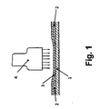
- Fig. 1 shows an arrangement comprising a support body 1, on which a flexible circuit board 2, 3 is arranged, wherein the flexible circuit board 2, 3 has a carrier layer 2, on which at least one electrical line 3 is arranged.
- the electrical line 3 of the flexible printed circuit board 2, 3 is thermally conductive and electrically conductively connected to the support body 1, wherein heat and electric current of the electrical line 3 to the support body 1 can be discharged.
- the electrical line 3 is at least partially directly on the support body 1. For this purpose, a part of the carrier layer 2 is removed, which lies between the electrical line 3 and the support body 1.
- the electrical line 3 is connected by welding material fit with the support body 1.
- the welding is carried out with a sonotrode 4. Specifically, ultrasound is used to connect the electrical wire 3 made of copper with the rigid and stiffening support body 1 made of aluminum.
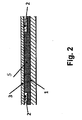
- Fig. 2 shows an arrangement in which the electrical line 3 is at least partially connected by an adhesive 5 to the support body 1, wherein the adhesive 5 is applied directly to the support body 1 and to the electrical line 3.
- adhesive 5 a conductive adhesive is used.
- the support body 1 is rigid and serves as a stiffening of the flexible printed circuit board 2, 3.
- the support body 1 has aluminum.
- the electrical line 3 is made of copper.
- the flexible printed circuit board 2, 3 can be processed by laser or punching. In particular, a part of the carrier layer 2 can be removed by punching or lasing. Thus, an electrical line 3 can be exposed and connected to the support body 1 thermally conductive and / or electrically conductive.
- the flexible printed circuit board 2, 3 has a carrier layer 2, which is preferably made of polyethylene naphthalate or polyimide.
- the electrical line 3 of the flexible printed circuit board 2, 3 is made of copper.
- the electrical line 3 can also have wider areas and be part of a network of electrical lines 3, which rests on the carrier layer 2.
- the electrical components are designed as so-called “surface mounted devices” (SMD). Such components are surface mounted components. In contrast to the conventional assembly of electrical circuit boards these components are not plugged with their connecting wires in a circuit board and soldered on the other side. In an SMD technique, the soldering takes place on the same side on which the assembly takes place.
- SMD surface mounted devices
Landscapes
- Engineering & Computer Science (AREA)
- Microelectronics & Electronic Packaging (AREA)
- Manufacturing & Machinery (AREA)
- Structure Of Printed Boards (AREA)
Abstract
Description
- Die Erfindung betrifft eine Anordnung gemäß dem Oberbegriff des Patentanspruchs 1.
- Aus dem Stand der Technik sind flexible Leiterplatten, so genannte "Flexible Printed Circuits" (FPC), bekannt. Eine flexible Leiterplatte weist üblicherweise eine Trägerschicht aus Polyethylennaphthalat oder Polyimid auf. Auf dieser Trägerschicht sind elektrische Leitungen oder ein Netzwerk aus elektrischen Leitungen aufgebracht.
- Auf einer flexiblen Leiterplatte können elektrische Bauteile, wie beispielsweise LEDs, angeordnet sein. Solche elektrischen Bauteile können als sogenannte "Surface Mounted Devices" (SMD) ausgestaltet sein. Diese Bauteile sind oberflächerlmontierte Bauteile.
- Vor diesem Hintergrund besteht das Bedürfnis nach einer Anordnung, bei welcher die Wärme zuverlässig abgeführt wird, die von wärmeerzeugenden SMD-Bauteilen, wie beispielsweise LEDs, erzeugt wird.
- Der Erfindung liegt daher die Aufgabe zugrunde, eine Anordnung der eingangs genannten Art derart auszugestalten und weiterzubilden, dass eine zuverlässige Abführung von Wärme sichergestellt ist, welche durch elektrische Bauteile erzeugt wird.
- Die vorliegende Erfindung löst die zuvor genannte Aufgabe durch eine Anordnung mit den Merkmalen des Patentanspruchs 1.
- Erfindungsgemäß ist zunächst erkannt worden, dass der Kunststoff einer Trägerschicht einer flexiblen Leiterplatte schlecht Wärme leitet. Weiter ist erkannt worden, dass ein Tragkörper eine erhebliche Wärmemenge aufnehmen kann. Der Tragkörper fungiert aufgrund seiner Masse insoweit als Kühlkörper. Erfindungsgemäß ist die elektrische Leitung der flexiblen Leiterplatte daher wärmeleitend und/ oder elektrisch leitend mit dem Tragkörper verbunden, wobei Wärme und/ oder elektrischer Strom der elektrischen Leitung an den Tragkörper abführbar ist. Hierdurch ist eine sehr gute Wärmeableitung der Wärme von wärmeerzeugenden Bauteilen ermöglicht.
- Folglich ist die eingangs genannte Aufgabe gelöst.
- Die elektrische Leitung könnte zumindest bereichsweise unmittelbar am Tragkörper anliegen. Hierdurch ist ein elektrischer Kontakt geringen Widerstands und ein hocheffektiver Wärmekontakt mit dem Tragkörper möglich. Es erfolgt eine direkte Ankopplung der elektrischen Leitungen einer flexiblen Leiterplatte an einen versteifenden Tragkörper.
- Vor diesem Hintergrund könnte die elektrische Leitung durch Verschweißen stoffschlüssig mit dem Tragkörper verbunden sein. Bevorzugt kann die Verbindung durch Ultraschalischweißen erfolgen. Ein Schweißprozess ist kostengünstig. Er kann rasch und ohne chemische Hilfsstoffe durchgeführt werden. Insoweit ist ein sortenreiner Aufbau der Anordnung möglich, wodurch diese leicht entsorgbar ist.
- Die elektrische Leitung könnte zumindest bereichsweise durch einen Klebstoff mit dem Tragkörper verbunden sein, wobei der Klebstoff unmittelbar am Tragkörper und an der elektrischen Leitung anliegt. Bevorzugt wird ein Klebstoff eingesetzt, der als Leitkleber ausgestaltet ist.
- Der Tragkörper könnte starr sein. Hierdurch ist eine Versteifung der Anordnung möglich.
- Der Tragkörper könnte Aluminium aufweisen. Bevorzugt ist der Tragkörper aus Aluminiumdruckguss gefertigt. Aluminium hat sich als besonders effektiver und leichter Kühlkörper zur Abführung von Wärme erwiesen.
- Die elektrische Leitung könnte aus Kupfer gefertigt sein. Kupfer ist besonders gut elektrisch leitfähig und geht mit Aluminium eine gute elektrische Leitungsverbindung und eine gute Wärmeleitungsverbindung ein.
- Die flexible Leiterplatte könnte mit elektrischen Bauteilen bestückt sein. Ein solches Bauteil könnte eine LED sein, um Licht zu erzeugen.
- Eine Anordnung der hier beschriebenen Art könnte als LED-Modul im Abblendlicht eines Kraftfahrzeugs verwendet werden.
- Konkret ist denkbar, LED-Module in automotiven Frontlichtapplikationen einzusetzen.
- Weiter ist denkbar, ein statisches Kurvenlicht, Fernlicht, Abblendlicht und Tagfahrlicht zu realisieren.
- In der Zeichnung zeigen
- Fig. 1
- eine schematische Darstellung der Durchführung eines Verfahrens zur Herstellung einer Anordnung, bei welcher die elektrischen Leitungen aus Kupfer durch Ultraschall mit einer Trägerplatte aus Aluminium verbunden sind, und
- Fig. 2
- eine schematische Darstellung einer Anordnung, bei welcher die elektrischen Leitungen aus Kupfer durch einen Klebstoff mit einer Trägerplatte aus Aluminium verbunden sind.
-
Fig. 1 zeigt eine Anordnung, umfassend einen Tragkörper 1, auf welchem eine flexible Leiterplatte 2, 3 angeordnet ist, wobei die flexible Leiterplatte 2, 3 eine Trägerschicht 2 aufweist, auf welcher mindestens eine elektrische Leitung 3 angeordnet ist. - Die elektrische Leitung 3 der flexiblen Leiterplatte 2, 3 ist wärmeleitend und elektrisch leitend mit dem Tragkörper 1 verbunden, wobei Wärme und elektrischer Strom der elektrischen Leitung 3 an den Tragkörper 1 abführbar ist. Die elektrische Leitung 3 liegt zumindest bereichsweise unmittelbar am Tragkörper 1 an. Hierzu ist ein Teil der Trägerschicht 2 entfernt, welche zwischen der elektrischen Leitung 3 und dem Tragkörper 1 liegt.
- Die elektrische Leitung 3 ist durch Verschweißen stoffschlüssig mit dem Tragkörper 1 verbunden. Das Verschweißen erfolgt mit einer Sonotrode 4. Konkret wird Ultraschall eingesetzt, um die elektrische Leitung 3 aus Kupfer mit dem starren und versteifenden Tragkörper 1 aus Aluminium zu verbinden.
-
Fig. 2 zeigt eine Anordnung, bei welcher die elektrische Leitung 3 zumindest bereichsweise durch einen Klebstoff 5 mit dem Tragkörper 1 verbunden ist, wobei der Klebstoff 5 unmittelbar am Tragkörper 1 und an der elektrischen Leitung 3 anliegt. Als Klebstoff 5 wird ein Leitkleber eingesetzt. - Der Tragkörper 1 ist starr und dient als Versteifung der flexiblen Leiterplatte 2, 3. Der Tragkörper 1 weist Aluminium auf. Die elektrische Leitung 3 ist aus Kupfer gefertigt.
- Die flexible Leiterplatte 2, 3 kann durch Lasern oder Stanzen bearbeitet werden. Insbesondere kann ein Teil der Trägerschicht 2 durch Stanzen oder Lasern entfernt werden. So kann eine elektrische Leitung 3 freigelegt und an den Tragkörper 1 wärmeleitend und/ oder elektrisch leitend angebunden werden.
- Die flexible Leiterplatte 2, 3 weist eine Trägerschicht 2 auf, welche bevorzugt aus Polyethylennaphthalat oder Polyimid gefertigt ist. Die elektrische Leitung 3 der flexiblen Leiterplatte 2, 3 ist aus Kupfer gefertigt. Die elektrische Leitung 3 kann auch breitere Flächen aufweisen und ein Teil eines Netzwerks aus elektrischen Leitungen 3 sein, welches auf der Trägerschicht 2 aufliegt.
- Auf der flexiblen Leiterplatte 2, 3 können elektrische Bauteile angeordnet sein. Die elektrischen Bauteile sind als sogenannte "Surface Mounted Devices" (SMD) ausgestaltet. Solche Bauteile sind oberflächenmontierte Bauteile. Im Gegensatz zur konventionellen Bestückung von elektrischen Leiterplatten werden diese Bauteile mit ihren Anschlussdrähten nicht in eine Platine gesteckt und auf der anderen Seite verlötet. Bei einer SMD-Technik erfolgt das Verlöten auf der gleichen Seite, auf der die Bestückung erfolgt.
Claims (8)
- Anordnung, umfassend einen Tragkörper (1), auf welchem eine flexible Leiterplatte (2, 3) angeordnet ist, wobei die flexible Leiterplatte (2, 3) eine Trägerschicht (2) aufweist, auf welcher mindestens eine elektrische Leitung (3) angeordnet ist,
dadurch gekennzeichnet, dass die elektrische Leitung (3) der flexiblen Leiterplatte (2, 3) wärmeleitend und/ oder elektrisch leitend mit dem Tragkörper (1) verbunden ist, wobei Wärme und/ oder elektrischer Strom der elektrischen Leitung (3) an den Tragkörper (1) abführbar ist. - Anordnung nach Anspruch 1, dadurch gekennzeichnet, dass die elektrische Leitung (3) zumindest bereichsweise unmittelbar am Tragkörper (1) anliegt.
- Anordnung nach Anspruch 1 oder 2, dadurch gekennzeichnet, dass die elektrische Leitung (3) durch Verschweißen stoffschlüssig mit dem Tragkörper (1) verbunden ist.
- Anordnung nach einem der voranstehenden Ansprüche, dadurch gekennzeichnet, dass die elektrische Leitung (3) zumindest bereichsweise durch einen Klebstoff (5) mit dem Tragkörper (1) verbunden ist, wobei der Klebstoff (5) unmittelbar am Tragkörper (1) und an der elektrischen Leitung (3) anliegt.
- Anordnung nach einem der voranstehenden Ansprüche, dadurch gekennzeichnet, dass der Tragkörper (1) starr ist.
- Anordnung nach einem der voranstehenden Ansprüche, dadurch gekennzeichnet, dass der Tragkörper (1) Aluminium aufweist.
- Anordnung nach einem der voranstehenden Ansprüche, dadurch gekennzeichnet, dass die elektrische Leitung (3) aus Kupfer gefertigt ist.
- Anordnung nach einem der voranstehenden Ansprüche, dadurch gekennzeichnet, dass die flexible Leiterplatte (2, 3) mit elektrischen Bauteilen bestückt ist.
Applications Claiming Priority (1)
| Application Number | Priority Date | Filing Date | Title |
|---|---|---|---|
| DE102013000169.2A DE102013000169A1 (de) | 2013-01-09 | 2013-01-09 | Anordnung mit einer flexiblen Leiterplatte |
Publications (1)
| Publication Number | Publication Date |
|---|---|
| EP2755456A1 true EP2755456A1 (de) | 2014-07-16 |
Family
ID=49619782
Family Applications (1)
| Application Number | Title | Priority Date | Filing Date |
|---|---|---|---|
| EP13005404.2A Ceased EP2755456A1 (de) | 2013-01-09 | 2013-11-18 | Anordnung mit einer flexiblen Leiterplatte und einer Wärmesenke |
Country Status (2)
| Country | Link |
|---|---|
| EP (1) | EP2755456A1 (de) |
| DE (1) | DE102013000169A1 (de) |
Cited By (1)
| Publication number | Priority date | Publication date | Assignee | Title |
|---|---|---|---|---|
| EP4380324A4 (de) * | 2021-10-12 | 2024-12-04 | LG Energy Solution, Ltd. | Leiterplatte, herstellungsverfahren dafür und batteriepack damit |
Citations (5)
| Publication number | Priority date | Publication date | Assignee | Title |
|---|---|---|---|---|
| USH650H (en) * | 1988-04-14 | 1989-07-04 | The United States Of America As Represented By The United States Department Of Energy | Double sided circuit board and a method for its manufacture |
| US5025348A (en) * | 1987-11-20 | 1991-06-18 | Casio Computer Co., Ltd. | Bonding structure of an electronic device and a method for manufacturing the same |
| EP0667736A1 (de) * | 1994-01-12 | 1995-08-16 | MAGNETEK S.p.A. | Laminare Platte für die Herstellung von gedruckten Schaltungen, daraus hergestellte gedruckte Schaltung und Verfahren zu ihrer Herstellung |
| US5896271A (en) * | 1997-07-21 | 1999-04-20 | Packard Hughes Interconnect Company | Integrated circuit with a chip on dot and a heat sink |
| DE10340705A1 (de) * | 2003-09-04 | 2005-04-21 | Fela Hilzinger Gmbh Leiterplat | Verfahren zum Herstellen einer Leiterplatte und Leiterplatte mit einem Metallträger als Leiterplattenkern |
Family Cites Families (2)
| Publication number | Priority date | Publication date | Assignee | Title |
|---|---|---|---|---|
| WO2005088711A1 (ja) * | 2004-03-16 | 2005-09-22 | Matsushita Electric Industrial Co., Ltd. | ドライバモジュール構造 |
| TWM315956U (en) * | 2006-12-29 | 2007-07-21 | Bothhand Entpr Inc | Improved structure of composite circuit substrate |
-
2013
- 2013-01-09 DE DE102013000169.2A patent/DE102013000169A1/de not_active Withdrawn
- 2013-11-18 EP EP13005404.2A patent/EP2755456A1/de not_active Ceased
Patent Citations (5)
| Publication number | Priority date | Publication date | Assignee | Title |
|---|---|---|---|---|
| US5025348A (en) * | 1987-11-20 | 1991-06-18 | Casio Computer Co., Ltd. | Bonding structure of an electronic device and a method for manufacturing the same |
| USH650H (en) * | 1988-04-14 | 1989-07-04 | The United States Of America As Represented By The United States Department Of Energy | Double sided circuit board and a method for its manufacture |
| EP0667736A1 (de) * | 1994-01-12 | 1995-08-16 | MAGNETEK S.p.A. | Laminare Platte für die Herstellung von gedruckten Schaltungen, daraus hergestellte gedruckte Schaltung und Verfahren zu ihrer Herstellung |
| US5896271A (en) * | 1997-07-21 | 1999-04-20 | Packard Hughes Interconnect Company | Integrated circuit with a chip on dot and a heat sink |
| DE10340705A1 (de) * | 2003-09-04 | 2005-04-21 | Fela Hilzinger Gmbh Leiterplat | Verfahren zum Herstellen einer Leiterplatte und Leiterplatte mit einem Metallträger als Leiterplattenkern |
Non-Patent Citations (2)
| Title |
|---|
| ANONYMOUS: "Timeline DE | TELSONIC Ultrasonics", 12 March 2018 (2018-03-12), XP055458742, Retrieved from the Internet <URL:https://www.telsonic.com/de/timeline-de/> [retrieved on 20180313] * |
| ANONYMOUS: "Ultraschall verbindet selbst Metall und Keramik In Bruchteilen von Sekunden ist alles erledigt", 21 February 2000 (2000-02-21), XP055458727, Retrieved from the Internet <URL:https://industrieanzeiger.industrie.de/allgemein/in-bruchteilen-von-sekunden-ist-alles-erledigt/> [retrieved on 20180313] * |
Cited By (1)
| Publication number | Priority date | Publication date | Assignee | Title |
|---|---|---|---|---|
| EP4380324A4 (de) * | 2021-10-12 | 2024-12-04 | LG Energy Solution, Ltd. | Leiterplatte, herstellungsverfahren dafür und batteriepack damit |
Also Published As
| Publication number | Publication date |
|---|---|
| DE102013000169A1 (de) | 2014-07-10 |
Similar Documents
| Publication | Publication Date | Title |
|---|---|---|
| EP1719189B1 (de) | Leuchtdioden-anordnung für eine hochleistungs-leuchtdiode und verfahren zur herstellung einer leuchtdioden-anordnung | |
| DE10063876B4 (de) | Aus einer Vielzahl von Leuchtdioden bestehende Lichtquelle | |
| DE102009019285A1 (de) | Beleuchtungssystem mit mindestens einem Leuchtband | |
| DE102020106492A1 (de) | Chip -package, verfahren zum bilden eines chip -packages, halbleitervorrichtung, halbleiteranordnung, dreiphasensystem, verfahren zum bilden einer halbleitervorrichtung und verfahren zum bilden einer halbleiteranordnung | |
| EP1445799A2 (de) | Kühleinrichtung für Halbleiter auf Leiterplatte | |
| DE102014002415B4 (de) | Servoverstärker mit Kühlstruktur, die eine Wärmesenke umfasst | |
| DE102011005251A1 (de) | Optoelektronische Transistorkontur (Transistor Outline, TO)-Hülsensockelbaugruppe, welche eine Konfiguration aufweist, die die Wärmedissipation verbessert und einen thermischen Widerstand reduziert | |
| DE102017208973A1 (de) | Elektronische baugruppe für beleuchtungsanwendungen, beleuchtungseinrichtung sowie verfahren zur herstellung einer elektronischen baugruppe | |
| DE102008019797A1 (de) | Kühlanordnung und Umrichter | |
| EP2141406A2 (de) | Leuchte | |
| WO2012130548A1 (de) | Elektronikmodul | |
| WO2012136579A1 (de) | Keramische leiterplatte mit al-kühlkörper | |
| WO2014056834A1 (de) | Verfahren zur herstellung einer lichterzeugungseinheit | |
| DE20120770U1 (de) | Oberflächenmontierte LED-Mehrfachanordnung und Beleuchtungseinrichtung damit | |
| DE102013000169A1 (de) | Anordnung mit einer flexiblen Leiterplatte | |
| EP4211996A1 (de) | Verfahren und gussteilherstellungsanlage zum herstellen eines elektromotor-gehäuses und elektromotor | |
| DE102012000907B4 (de) | Elektrogerät | |
| DE102012202562A1 (de) | Mehrschichtige leiterplatte | |
| DE102012211143A1 (de) | Träger für elektrisches bauelement mit wärmeleitkörper | |
| DE102019116021B4 (de) | Flexible Leiterplatte mit thermisch leitender Verbindung zu einer Wärmesenke | |
| DE10349775B4 (de) | Schaltungsträger für Leuchtdioden | |
| DE112007002337T5 (de) | Elektrische Schaltungsbaugruppe für Hochleistungselektronik | |
| DE10250697A1 (de) | Leiterplatte | |
| EP3123841A1 (de) | Transluzente mit led bestückte platinen und/oder kühlkörper | |
| EP2845235B1 (de) | Led-anordnung |
Legal Events
| Date | Code | Title | Description |
|---|---|---|---|
| PUAI | Public reference made under article 153(3) epc to a published international application that has entered the european phase |
Free format text: ORIGINAL CODE: 0009012 |
|
| 17P | Request for examination filed |
Effective date: 20131118 |
|
| AK | Designated contracting states |
Kind code of ref document: A1 Designated state(s): AL AT BE BG CH CY CZ DE DK EE ES FI FR GB GR HR HU IE IS IT LI LT LU LV MC MK MT NL NO PL PT RO RS SE SI SK SM TR |
|
| AX | Request for extension of the european patent |
Extension state: BA ME |
|
| R17P | Request for examination filed (corrected) |
Effective date: 20150113 |
|
| RBV | Designated contracting states (corrected) |
Designated state(s): AL AT BE BG CH CY CZ DE DK EE ES FI FR GB GR HR HU IE IS IT LI LT LU LV MC MK MT NL NO PL PT RO RS SE SI SK SM TR |
|
| RAP1 | Party data changed (applicant data changed or rights of an application transferred) |
Owner name: MEKTEC EUROPE GMBH |
|
| STAA | Information on the status of an ep patent application or granted ep patent |
Free format text: STATUS: EXAMINATION IS IN PROGRESS |
|
| 17Q | First examination report despatched |
Effective date: 20171031 |
|
| STAA | Information on the status of an ep patent application or granted ep patent |
Free format text: STATUS: THE APPLICATION HAS BEEN REFUSED |
|
| 18R | Application refused |
Effective date: 20180506 |