EP2755231A1 - Method for controlling concentration of donor in ga2o3-based single crystal - Google Patents
Method for controlling concentration of donor in ga2o3-based single crystal Download PDFInfo
- Publication number
- EP2755231A1 EP2755231A1 EP12829259.6A EP12829259A EP2755231A1 EP 2755231 A1 EP2755231 A1 EP 2755231A1 EP 12829259 A EP12829259 A EP 12829259A EP 2755231 A1 EP2755231 A1 EP 2755231A1
- Authority
- EP
- European Patent Office
- Prior art keywords
- single crystal
- donor
- based single
- concentration
- region
- Prior art date
- Legal status (The legal status is an assumption and is not a legal conclusion. Google has not performed a legal analysis and makes no representation as to the accuracy of the status listed.)
- Granted
Links
Images


Classifications
-
- H—ELECTRICITY
- H10—SEMICONDUCTOR DEVICES; ELECTRIC SOLID-STATE DEVICES NOT OTHERWISE PROVIDED FOR
- H10D—INORGANIC ELECTRIC SEMICONDUCTOR DEVICES
- H10D62/00—Semiconductor bodies, or regions thereof, of devices having potential barriers
- H10D62/80—Semiconductor bodies, or regions thereof, of devices having potential barriers characterised by the materials
-
- H—ELECTRICITY
- H10—SEMICONDUCTOR DEVICES; ELECTRIC SOLID-STATE DEVICES NOT OTHERWISE PROVIDED FOR
- H10D—INORGANIC ELECTRIC SEMICONDUCTOR DEVICES
- H10D62/00—Semiconductor bodies, or regions thereof, of devices having potential barriers
- H10D62/10—Shapes, relative sizes or dispositions of the regions of the semiconductor bodies; Shapes of the semiconductor bodies
- H10D62/124—Shapes, relative sizes or dispositions of the regions of semiconductor bodies or of junctions between the regions
- H10D62/126—Top-view geometrical layouts of the regions or the junctions
-
- H—ELECTRICITY
- H10—SEMICONDUCTOR DEVICES; ELECTRIC SOLID-STATE DEVICES NOT OTHERWISE PROVIDED FOR
- H10D—INORGANIC ELECTRIC SEMICONDUCTOR DEVICES
- H10D62/00—Semiconductor bodies, or regions thereof, of devices having potential barriers
- H10D62/60—Impurity distributions or concentrations
-
- H—ELECTRICITY
- H10—SEMICONDUCTOR DEVICES; ELECTRIC SOLID-STATE DEVICES NOT OTHERWISE PROVIDED FOR
- H10D—INORGANIC ELECTRIC SEMICONDUCTOR DEVICES
- H10D62/00—Semiconductor bodies, or regions thereof, of devices having potential barriers
- H10D62/80—Semiconductor bodies, or regions thereof, of devices having potential barriers characterised by the materials
- H10D62/82—Heterojunctions
-
- H—ELECTRICITY
- H10—SEMICONDUCTOR DEVICES; ELECTRIC SOLID-STATE DEVICES NOT OTHERWISE PROVIDED FOR
- H10P—GENERIC PROCESSES OR APPARATUS FOR THE MANUFACTURE OR TREATMENT OF DEVICES COVERED BY CLASS H10
- H10P30/00—Ion implantation into wafers, substrates or parts of devices
- H10P30/20—Ion implantation into wafers, substrates or parts of devices into semiconductor materials, e.g. for doping
- H10P30/202—Ion implantation into wafers, substrates or parts of devices into semiconductor materials, e.g. for doping characterised by the semiconductor materials
-
- H—ELECTRICITY
- H10—SEMICONDUCTOR DEVICES; ELECTRIC SOLID-STATE DEVICES NOT OTHERWISE PROVIDED FOR
- H10P—GENERIC PROCESSES OR APPARATUS FOR THE MANUFACTURE OR TREATMENT OF DEVICES COVERED BY CLASS H10
- H10P30/00—Ion implantation into wafers, substrates or parts of devices
- H10P30/20—Ion implantation into wafers, substrates or parts of devices into semiconductor materials, e.g. for doping
- H10P30/21—Ion implantation into wafers, substrates or parts of devices into semiconductor materials, e.g. for doping of electrically active species
-
- H—ELECTRICITY
- H10—SEMICONDUCTOR DEVICES; ELECTRIC SOLID-STATE DEVICES NOT OTHERWISE PROVIDED FOR
- H10P—GENERIC PROCESSES OR APPARATUS FOR THE MANUFACTURE OR TREATMENT OF DEVICES COVERED BY CLASS H10
- H10P30/00—Ion implantation into wafers, substrates or parts of devices
- H10P30/20—Ion implantation into wafers, substrates or parts of devices into semiconductor materials, e.g. for doping
- H10P30/22—Ion implantation into wafers, substrates or parts of devices into semiconductor materials, e.g. for doping using masks
-
- H—ELECTRICITY
- H10—SEMICONDUCTOR DEVICES; ELECTRIC SOLID-STATE DEVICES NOT OTHERWISE PROVIDED FOR
- H10P—GENERIC PROCESSES OR APPARATUS FOR THE MANUFACTURE OR TREATMENT OF DEVICES COVERED BY CLASS H10
- H10P30/00—Ion implantation into wafers, substrates or parts of devices
- H10P30/20—Ion implantation into wafers, substrates or parts of devices into semiconductor materials, e.g. for doping
- H10P30/222—Ion implantation into wafers, substrates or parts of devices into semiconductor materials, e.g. for doping characterised by the angle between the ion beam and the crystal planes or the main crystal surface
-
- H—ELECTRICITY
- H10—SEMICONDUCTOR DEVICES; ELECTRIC SOLID-STATE DEVICES NOT OTHERWISE PROVIDED FOR
- H10P—GENERIC PROCESSES OR APPARATUS FOR THE MANUFACTURE OR TREATMENT OF DEVICES COVERED BY CLASS H10
- H10P30/00—Ion implantation into wafers, substrates or parts of devices
- H10P30/20—Ion implantation into wafers, substrates or parts of devices into semiconductor materials, e.g. for doping
- H10P30/28—Ion implantation into wafers, substrates or parts of devices into semiconductor materials, e.g. for doping characterised by an annealing step, e.g. for activation of dopants
Definitions
- the invention relates to a method for controlling a concentration of a donor in a Ga 2 O 3 -based single crystal and, in particular, to a method for controlling the concentration of a donor in a Ga 2 O 3 -based single crystal using ion implantation process.
- a method is known in which a Group IV element such as Si or Sn is added while growing a Ga 2 O 3 sin crystal to impart conductivity to the Ga 2 O 3 single crystal (see, e.g., PTL 1).
- a method is known in which a ⁇ -Ga 2 O 3 crystal is heteroepitaxially grown on a sapphire substrate while adding an impurity such as Sn to form a ⁇ -Ga 2 O 3 crystal film having conductivity (see, e.g., PTL 2 ).
- a method in which an impurity ion is introduced into a SiC crystal by ion implantation process is also known (see, e.g., PTL 3 ).
- the ion implantation process is advantageous in that, e.g., an impurity concentration can be controlled after forming a base crystal or it is possible to locally introduce an impurity relatively easily.
- a method for controlling a concentration of a donor in a Ga 2 O 3 -based single crystal as defined in [1] to [5] below is provided so as to achieve the above object.
- a method for controlling the concentration of a donor in a Ga 2 O 3 -based single crystal using ion implantation process can be provided that allows the formation of a highly electrically conductive region in a Ga 2 O 3 -based single crystal.
- introduction of a donor impurity into a Ga 2 O 3 -based single crystal using the ion implantation process and subsequent annealing treatment performed under predetermined conditions allow a high-donor-concentration region having superior electrical conductivity to be formed in the Ga 2 O 3 based crystal.
- a method for controlling the concentration of a donor in a ⁇ -Ga 2 O 3 -based single crystal will be described in detail as an example.
- the Ga 2 O 3 -based single crystal in the present embodiment is not limited to a ⁇ -Ga 2 O 3 -based single crystal and may be a Ga 2 O 3 -based single crystal having another structure such as ⁇ -Ga 2 O 3 -based single crystal.
- FIGS. 1A to 1D are cross sectional views of a ⁇ -Ga 2 O 3 -based crystal, showing an example of ion implantation process.
- a mask 2 is formed on a ⁇ -Ga 2 O 3 -based single crystal 1 , as shown in FIG.1A .
- the mask 2 is formed using a photolithography technique, etc.
- a donor impurity is implanted into the ⁇ -Ga 2 O 3 -based single crystal 1 by ion implantation and a donor impurity implantation region 3 is thereby formed on a surface of the ⁇ -Ga 2 O 3 -based single crystal 1 .
- the donor impurity implantation region 3 is formed in a partial region of the surface of the ⁇ -Ga 2 O 3 -based single crystal 1 .
- the donor impurity concentration in the donor impurity implantation region 3 is higher than that of the ⁇ -Ga 2 O 3 -based single crystal 1 in the region with no impurity implanted.
- the donor impurity implantation region 3 may be formed on the entire surface of the ⁇ -Ga 2 O 3 -based single crystal 1 by ion implantation without using the mask 2 .
- the mask 2 is removed, as shown in FIG 1C .
- the donor impurity in the donor impurity implantation region 3 is activated by performing annealing treatment at not less than 800 °C, thereby forming a high-donor-concentration region 4 having a high donor concentration, as shown in FIG.1D .
- damage on the ⁇ -Ga 2 O 3 -based single crystal 1 caused by the ion implantation can be repaired by this annealing treatment.
- the annealing treatment conditions are, e.g., not less than 800 °C in an inert atmosphere such as nitrogen atmosphere or argon atmosphere, or not less than 800 °C and not more than 950 °C in an oxygen atmosphere.
- the ⁇ -Ga 2 O 3 -based single crystal 1 is constructed from a ⁇ -Ga 2 O 3 single crystal or a ⁇ -Ga 2 O 3 single crystal doped with elements such as Al and In. It may be, e.g., a (Ga x Al y In (1-x-y ) 2 O 3 ( 0 ⁇ x ⁇ 1 , 0 ⁇ y ⁇ 1 , 0 ⁇ x+y ⁇ 1 ) crystal which is a ⁇ -Ga 2 O 3 crystal doped with Al and In.
- the band gap is widened by adding Al and is narrowed by adding In.
- the ⁇ -Ga 2 O 3 -based single crystal 1 is a ⁇ -Ga 2 O 3 -based single crystal substrate or a ⁇ -Ga 2 O 3 -based crystal film formed on a supporting substrate.
- Group IV elements such as Si, Sn and Ge are used as a donor impurity to be introduced into the ⁇ -Ga 2 O 3 -based single crystal 1 by the ion implantation process.
- FIG. 2 is a graph showing a relation between annealing treatment temperature in a nitrogen atmosphere after ion implantation and conductivity of the ⁇ -Ga 2 O 3 single crystal substrate as the ⁇ -Ga 2 O 3 based single crystal.
- the vertical axis in FIG. 2 indicates a difference between donor density and acceptor density (Nd-Na) per unit cubic centimeter in the high-donor-concentration region of the ⁇ -Ga 2 O 3 single crystal substrate, i.e., indicates a conductivity level of the high-donor-concentration region of the ⁇ -Ga 2 O 3 single crystal substrate which is an n-type semiconductor.
- the horizontal axis in FIG.2 indicates annealing treatment temperature in a nitrogen atmosphere. The annealing treatment is performed for 30 minutes each.
- the high-donor-concentration region is a box-shaped region having a depth of 200 nm and is formed by ion-implanting Si or Sn with a concentration of 1 x 10 19 /cm 3 into a ⁇ -Ga 2 O 3 single crystal substrate having a donor concentration of 3 x 10 17 /cm 3 .
- the high-donor-concentration region is formed by vertically implanting a donor impurity on a (010) plane, as a main surface, of the ⁇ -Ga 2 O 3 single crystal substrate.
- the filled square and the filled triangle in FIG.2 indicate Nd-Na values when respectively implanting Si and Sn as a donor impurity. Meanwhile, the open circle indicates Nd-Na values when the donor impurity is not implanted.
- the Nd-Na value is increased by annealing treatment at not less than 800 °C in case of implanting Si as well as in case of implanting Sn. That is, the annealing treatment at not less than 800 °C in a nitrogen atmosphere after the ion implantation allows high conductivity to be imparted to the ⁇ -Ga 2 O 3 single crystal substrate. It should be noted that, when the donor impurity is not implanted, the Nd-Na value is not greatly increased even if the annealing treatment temperature is raised.
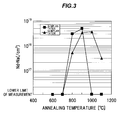
- FIG.3 is a graph showing a relation between annealing treatment temperature in an oxygen atmosphere after ion implantation and conductivity of the ⁇ -Ga 2 O 3 single crystal substrate as the ⁇ -Ga 2 O 3 -based single crystal.
- the vertical axis in FIG. 3 indicates a difference between donor density and acceptor density (Nd-Na) per unit cubic centimeter in the high-donor-concentration region of the ⁇ -Ga 2 O 3 single crystal substrate, i.e., indicates a conductivity level of the high-donor-concentration region of the ⁇ -Ga 2 O 3 single crystal substrate which is an n-type semiconductor.
- the horizontal axis in FIG.3 indicates annealing treatment temperature in an oxygen atmosphere. The annealing treatment is performed for 30 minutes each.
- the filled square and the filled triangle in FIG.3 indicate the Nd-Na values when respectively implanting Si and Sn as a donor impurity.
- the Nd-Na value is increased by annealing treatment at not less than 800 °C and not more than 950 °C when Si is implanted. Also, the Nd-Na value is increased by annealing treatment at not less than 800 °C and not more than 1100 °C when Sn is implanted. That is, the annealing treatment at not less than 800 °C and not more than 950 °C in an oxygen atmosphere after the ion implantation allows high conductivity to be imparted to the ⁇ -Ga 2 O 3 single crystal substrate.
- introduction of a donor impurity into a ⁇ -Ga 2 O 3 -based crystal using the ion implantation process and subsequent annealing treatment performed under predetermined conditions allow a high-donor-concentration region having superior electrical conductivity to be formed in the ⁇ -Ga 2 O 3 -based crystal. Since the high-donor-concentration region is formed using the ion implantation process, it is possible to control the donor concentration in the high-donor-concentration region after forming the ⁇ -Ga 2 O 3 -based crystal and thereby to impart a desired conductivity. In addition, use of a mask, etc., allows the high-donor-concentration region to be locally formed in the ⁇ -Ga 2 O 3- based crystal.
- a method for controlling the concentration of a donor in a Ga 2 O 3 -based single crystal using ion implantation process, which allows a highly electrically conductive region to be formed in a Ga 2 O 3 -based single crystal, is provided.
Landscapes
- Crystals, And After-Treatments Of Crystals (AREA)
- Element Separation (AREA)
- Physical Vapour Deposition (AREA)
Abstract
Description
- The invention relates to a method for controlling a concentration of a donor in a Ga2O3-based single crystal and, in particular, to a method for controlling the concentration of a donor in a Ga2O3-based single crystal using ion implantation process.
- As a conventional method of forming a Ga2O3 single crystal, a method is known in which a Group IV element such as Si or Sn is added while growing a Ga2O3 sin crystal to impart conductivity to the Ga2O3 single crystal (see, e.g., PTL 1).
- Meanwhile, as another conventional method of forming a Ga2O3 single crystal, a method is known in which a β-Ga2O3 crystal is heteroepitaxially grown on a sapphire substrate while adding an impurity such as Sn to form a β-Ga2O3 crystal film having conductivity (see, e.g., PTL 2).
- A method in which an impurity ion is introduced into a SiC crystal by ion implantation process is also known (see, e.g., PTL 3).
-
- [PTL 1]
JP-A2405-235961 - [PTL 2]
Japanese Patent No.4083396 - [PTL 3]
Japanese Patent No.4581270 - In the meantime, it is difficult to use the ion implantation process to introduce an impurity into an oxide single crystal such as Ga2O3 single crystal for the purpose of imparting conductivity. This is because the oxide is likely to be damaged by ion implantation and such damage is difficult to be sufficiently repaired even if annealing treatment is performed after the ion implantation. It is believed that, in the oxide single crystal, oxygen deficiency during the ion implantation increases damage on the crystal.
- However, the ion implantation process is advantageous in that, e.g., an impurity concentration can be controlled after forming a base crystal or it is possible to locally introduce an impurity relatively easily.
- It is an object of the invention to provide a method for controlling the concentration of a donor in a Ga2O3-based single crystal using ion implantation process that allows the formation of a highly electrically conductive region in a Ga2O3-base single crystal.
- According to one embodiment of the invention, a method for controlling a concentration of a donor in a Ga2O3-based single crystal as defined in [1] to [5] below is provided so as to achieve the above object.
-
- [1] A method for controlling a concentration of a donor in a Ga2O3-based single crystal, comprising:
- a step of introducing a Group IV element as a donor impurity into a Ga2O3-based single crystal by ion implantation process so as to form a donor impurity implantation region having a higher concentration of the Group IV element than the region without implanting the Group IV element in the Ga2O3-based single crystal; and
- a step of activating the Group IV element present in the donor impurity implantation region by annealing treatment at a temperature not less than 800°C to form a high-donor-concentration region.
- [2] The method for controlling a concentration of a donor in a Ga2O3-based single crystal according to [1], wherein the annealing treatment is conducted under a condition of not less than 800°C in a nitrogen atmosphere.
- [3] The method for controlling a concentration of a donor in a Ga2O3-based single crystal according to [1], wherein the annealing treatment is conducted under a condition of not less than 800°C and not more than 950°C in an oxygen atmosphere.
- [4] The method for controlling a concentration of a donor in a Ga2O3-based single crystal according to one of [1] to [3], wherein the Group IV element is introduced into a partial region of a surface of the Ga2O3-based single crystal using a mask formed on the Ga2O3-based single crystal so as to form the donor impurity implantation region in the partial region of the surface of the Ga2O3-based single crystal.
- [5] The method for controlling a concentration of a donor in a Ga2O3-based single crystal according to [1], wherein the Ga2O3-based single crystal comprises a Ga2O3-based single crystal substrate or a Ga2O3-based crystal film formed on a supporting substrate.
- According to an embodiment of the invention, a method for controlling the concentration of a donor in a Ga2O3-based single crystal using ion implantation process can be provided that allows the formation of a highly electrically conductive region in a Ga2O3-based single crystal.
-
- [
FIG. 1A ]
FIG. 1A is a cross sectional view of a β-Ga2O3-based crystal, showing an example of ion implantation process. - [
FIG. 1B ]
FIG. 1B is a cross sectional view of the β-Ga2O3-based crystal, showing the example of ion implantation process. - [
FIG.1C ]
FIG. 1C is a cross sectional view of the β-Ga2O3-based crystal, showing the example of ion implantation process. - [
FIG. 1D ]
FIG. 1D is a cross sectional view of the β-Ga2O3-based crystal, showing the example of ion implantation process. -
FIG.2 ]
FIG.2 is a graph showing a relation between annealing treatment temperature in a nitrogen atmosphere after ion implantation and conductivity of a β-Ga2O3 crystal film. - [
FIG.3 ]
FIG.3 is a graph showing a relation between annealing treatment temperature in an oxygen atmosphere after ion implantation and conductivity of a β-Ga2O3 crystal film. - According to the present embodiment, introduction of a donor impurity into a Ga2O3-based single crystal using the ion implantation process and subsequent annealing treatment performed under predetermined conditions allow a high-donor-concentration region having superior electrical conductivity to be formed in the Ga2O3 based crystal. Following is an embodiment thereof and a method for controlling the concentration of a donor in a β-Ga2O3-based single crystal will be described in detail as an example. It should be noted that the Ga2O3-based single crystal in the present embodiment is not limited to a β-Ga2O3-based single crystal and may be a Ga2O3-based single crystal having another structure such as α-Ga2O3-based single crystal.
-
FIGS. 1A to 1D are cross sectional views of a β-Ga2O3-based crystal, showing an example of ion implantation process. - Firstly, a
mask 2 is formed on a β-Ga2O3-basedsingle crystal 1, as shown inFIG.1A . Themask 2 is formed using a photolithography technique, etc. - Next, as shown in
FIG.1B , a donor impurity is implanted into the β-Ga2O3-basedsingle crystal 1 by ion implantation and a donorimpurity implantation region 3 is thereby formed on a surface of the β-Ga2O3-basedsingle crystal 1. At this point, since the donor impurity is not implanted into a region of the β-Ga2O3-basedsingle crystal 1 covered with themask 2, the donorimpurity implantation region 3 is formed in a partial region of the surface of the β-Ga2O3-basedsingle crystal 1. The donor impurity concentration in the donorimpurity implantation region 3 is higher than that of the β-Ga2O3-basedsingle crystal 1 in the region with no impurity implanted. - Alternatively, the donor
impurity implantation region 3 may be formed on the entire surface of the β-Ga2O3-basedsingle crystal 1 by ion implantation without using themask 2. In addition, it is possible to control depth or concentration distribution of the donorimpurity implantation region 3 by adjusting the ion implantation conditions. - Next, the
mask 2 is removed, as shown inFIG 1C . - After that, the donor impurity in the donor
impurity implantation region 3 is activated by performing annealing treatment at not less than 800°C, thereby forming a high-donor-concentration region 4 having a high donor concentration, as shown inFIG.1D . In addition, damage on the β-Ga2O3-basedsingle crystal 1 caused by the ion implantation can be repaired by this annealing treatment. In detail, the annealing treatment conditions are, e.g., not less than 800°C in an inert atmosphere such as nitrogen atmosphere or argon atmosphere, or not less than 800°C and not more than 950°C in an oxygen atmosphere. - The β-Ga2O3-based
single crystal 1 is constructed from a β-Ga2O3 single crystal or a β-Ga2O3 single crystal doped with elements such as Al and In. It may be, e.g., a (GaxAlyIn(1-x-y)2O3 (0<x<1, 0≤y≤1, 0≤x+y≤1) crystal which is a β-Ga2O3 crystal doped with Al and In. The band gap is widened by adding Al and is narrowed by adding In. - The β-Ga2O3-based
single crystal 1 is a β-Ga2O3-based single crystal substrate or a β-Ga2O3-based crystal film formed on a supporting substrate. - Group IV elements such as Si, Sn and Ge are used as a donor impurity to be introduced into the β-Ga2O3-based
single crystal 1 by the ion implantation process. -
FIG. 2 is a graph showing a relation between annealing treatment temperature in a nitrogen atmosphere after ion implantation and conductivity of the β-Ga2O3 single crystal substrate as the β-Ga2O3 based single crystal. The vertical axis inFIG. 2 indicates a difference between donor density and acceptor density (Nd-Na) per unit cubic centimeter in the high-donor-concentration region of the β-Ga2O3 single crystal substrate, i.e., indicates a conductivity level of the high-donor-concentration region of the β-Ga2O3 single crystal substrate which is an n-type semiconductor. The horizontal axis inFIG.2 indicates annealing treatment temperature in a nitrogen atmosphere. The annealing treatment is performed for 30 minutes each. - The high-donor-concentration region is a box-shaped region having a depth of 200 nm and is formed by ion-implanting Si or Sn with a concentration of 1x10 19/cm3 into a β-Ga2O3 single crystal substrate having a donor concentration of 3x10 17/cm3. In addition, the high-donor-concentration region is formed by vertically implanting a donor impurity on a (010) plane, as a main surface, of the β-Ga2O3 single crystal substrate.
- The filled square and the filled triangle in
FIG.2 indicate Nd-Na values when respectively implanting Si and Sn as a donor impurity. Meanwhile, the open circle indicates Nd-Na values when the donor impurity is not implanted. - As shown in
FIG.2 , the Nd-Na value is increased by annealing treatment at not less than 800°C in case of implanting Si as well as in case of implanting Sn. That is, the annealing treatment at not less than 800°C in a nitrogen atmosphere after the ion implantation allows high conductivity to be imparted to the β-Ga2O3 single crystal substrate. It should be noted that, when the donor impurity is not implanted, the Nd-Na value is not greatly increased even if the annealing treatment temperature is raised. -
FIG.3 is a graph showing a relation between annealing treatment temperature in an oxygen atmosphere after ion implantation and conductivity of the β-Ga2O3 single crystal substrate as the β-Ga2O3-based single crystal. The vertical axis inFIG. 3 indicates a difference between donor density and acceptor density (Nd-Na) per unit cubic centimeter in the high-donor-concentration region of the β-Ga2O3 single crystal substrate, i.e., indicates a conductivity level of the high-donor-concentration region of the β-Ga2O3 single crystal substrate which is an n-type semiconductor. The horizontal axis inFIG.3 indicates annealing treatment temperature in an oxygen atmosphere. The annealing treatment is performed for 30 minutes each. - The filled square and the filled triangle in
FIG.3 indicate the Nd-Na values when respectively implanting Si and Sn as a donor impurity. - As shown in
FIG.3 , the Nd-Na value is increased by annealing treatment at not less than 800°C and not more than 950°C when Si is implanted. Also, the Nd-Na value is increased by annealing treatment at not less than 800°C and not more than 1100°C when Sn is implanted. That is, the annealing treatment at not less than 800°C and not more than 950°C in an oxygen atmosphere after the ion implantation allows high conductivity to be imparted to the β-Ga2O3 single crystal substrate. - According to the present embodiment, introduction of a donor impurity into a β-Ga2O3-based crystal using the ion implantation process and subsequent annealing treatment performed under predetermined conditions allow a high-donor-concentration region having superior electrical conductivity to be formed in the β-Ga2O3-based crystal. Since the high-donor-concentration region is formed using the ion implantation process, it is possible to control the donor concentration in the high-donor-concentration region after forming the β-Ga2O3-based crystal and thereby to impart a desired conductivity. In addition, use of a mask, etc., allows the high-donor-concentration region to be locally formed in the β-Ga2O3-based crystal.
- Although the embodiment the invention has been described above, the invention according to claims is not to be limited to the above-mentioned embodiment. Further, it should be noted that all combinations of the features described in the embodiment are not necessary to solve the problem of the invention.
- A method for controlling the concentration of a donor in a Ga2O3-based single crystal using ion implantation process, which allows a highly electrically conductive region to be formed in a Ga2O3-based single crystal, is provided.
-
- 1: β-Ga2O3-based single crystal
- 2: mask
- 3: donor impurity implantation region
- 4: high-donor-concentration region
Claims (5)
- A method for controlling a concentration of a donor in a Ga2O3-based single crystal, comprising:a step of introducing a Group IV element as a donor impurity into a Ga2O3-based single crystal by ion implantation process so as to form a donor impurity implantation region having a higher concentration of the Group IV element than a region without implanting the Group IV element in the Ga2O3-based single crystal; anda step of activating the Group IV element present in the donor impurity implantation region by annealing treatment at a temperature not less than 800°C to form a high-donor-concentration region.
- The method for controlling a concentration of a donor in a Ga2O3-based single crystal according to claim 1, wherein the annealing treatment is conducted under a condition of not less than 800°C in a nitrogen atmosphere.
- The method for controlling a concentration of a donor in a Ga2O3-based single crystal according to claim 1, wherein the annealing treatment is conducted under a condition of not less than 800°C and not more than 950°C in an oxygen atmosphere.
- The method for controlling a concentration of a donor in a Ga2O3-based single crystal according to one of claims 1 to 3, wherein the Group IV element is introduced into a partial region of a surface of the Ga2O3-based single crystal using a mask formed on the Ga2O3-based single crystal so as to form the donor impurity implantation region in the partial region of the surface of the Ga2O3-based single crystal.
- The method for controlling a concentration of a donor in a Ga2O3-based single crystal according to claim 1, wherein the Ga2O3-based single crystal comprises a Ga2O3-based single crystal substrate or a Ga2O3-based crystal film formed on a supporting substrate.
Priority Applications (1)
| Application Number | Priority Date | Filing Date | Title |
|---|---|---|---|
| EP19152461.0A EP3493245B1 (en) | 2011-09-08 | 2012-08-02 | Ga2o3-based single crystal having a region with higher donor concentration than a surrounding region |
Applications Claiming Priority (2)
| Application Number | Priority Date | Filing Date | Title |
|---|---|---|---|
| JP2011196434 | 2011-09-08 | ||
| PCT/JP2012/069710 WO2013035465A1 (en) | 2011-09-08 | 2012-08-02 | Method for controlling concentration of donor in ga2o3-based single crystal |
Related Child Applications (2)
| Application Number | Title | Priority Date | Filing Date |
|---|---|---|---|
| EP19152461.0A Division EP3493245B1 (en) | 2011-09-08 | 2012-08-02 | Ga2o3-based single crystal having a region with higher donor concentration than a surrounding region |
| EP19152461.0A Division-Into EP3493245B1 (en) | 2011-09-08 | 2012-08-02 | Ga2o3-based single crystal having a region with higher donor concentration than a surrounding region |
Publications (3)
| Publication Number | Publication Date |
|---|---|
| EP2755231A1 true EP2755231A1 (en) | 2014-07-16 |
| EP2755231A4 EP2755231A4 (en) | 2015-04-08 |
| EP2755231B1 EP2755231B1 (en) | 2019-05-22 |
Family
ID=47831917
Family Applications (2)
| Application Number | Title | Priority Date | Filing Date |
|---|---|---|---|
| EP19152461.0A Active EP3493245B1 (en) | 2011-09-08 | 2012-08-02 | Ga2o3-based single crystal having a region with higher donor concentration than a surrounding region |
| EP12829259.6A Active EP2755231B1 (en) | 2011-09-08 | 2012-08-02 | Method for controlling the concentration of donors in ga2o3-based single crystal |
Family Applications Before (1)
| Application Number | Title | Priority Date | Filing Date |
|---|---|---|---|
| EP19152461.0A Active EP3493245B1 (en) | 2011-09-08 | 2012-08-02 | Ga2o3-based single crystal having a region with higher donor concentration than a surrounding region |
Country Status (5)
| Country | Link |
|---|---|
| US (2) | US8951897B2 (en) |
| EP (2) | EP3493245B1 (en) |
| JP (2) | JP5745073B2 (en) |
| CN (2) | CN106098756B (en) |
| WO (1) | WO2013035465A1 (en) |
Cited By (1)
| Publication number | Priority date | Publication date | Assignee | Title |
|---|---|---|---|---|
| EP3493245A1 (en) | 2011-09-08 | 2019-06-05 | Tamura Corporation | Ga2o3-based single crystal having a region with higher donor concentration than a surrounding region |
Families Citing this family (10)
| Publication number | Priority date | Publication date | Assignee | Title |
|---|---|---|---|---|
| WO2013035842A1 (en) * | 2011-09-08 | 2013-03-14 | 株式会社タムラ製作所 | Ga2O3 SEMICONDUCTOR ELEMENT |
| JP6142357B2 (en) * | 2013-03-01 | 2017-06-07 | 株式会社タムラ製作所 | Method for controlling donor concentration of Ga2O3-based single crystal and method for forming ohmic contact |
| JP2016031953A (en) * | 2014-07-25 | 2016-03-07 | 株式会社タムラ製作所 | Semiconductor device and method for manufacturing the same, semiconductor substrate, and crystal laminate structure |
| JP5828568B1 (en) * | 2014-08-29 | 2015-12-09 | 株式会社タムラ製作所 | Semiconductor device and manufacturing method thereof |
| JP2017041593A (en) * | 2015-08-21 | 2017-02-23 | 株式会社タムラ製作所 | Method for forming Ga2O3-based crystal film |
| CN106868593B (en) * | 2017-01-06 | 2019-04-19 | 中国科学院上海光学精密机械研究所 | High conductivity co-doped gallium oxide crystal and preparation method thereof |
| CN109671612B (en) * | 2018-11-15 | 2020-07-03 | 中国科学院上海微系统与信息技术研究所 | A kind of gallium oxide semiconductor structure and preparation method thereof |
| JP2022109466A (en) * | 2021-01-15 | 2022-07-28 | 株式会社デンソー | Method for manufacturing semiconductor device |
| US12532530B2 (en) | 2021-09-09 | 2026-01-20 | The Regents Of The University Of Michigan | Doped aluminum-alloyed gallium oxide and ohmic contacts |
| JP2024050122A (en) * | 2022-09-29 | 2024-04-10 | 株式会社ノベルクリスタルテクノロジー | Method for growing single crystal, method for manufacturing semiconductor substrate, and semiconductor substrate |
Family Cites Families (21)
| Publication number | Priority date | Publication date | Assignee | Title |
|---|---|---|---|---|
| JPH01286308A (en) * | 1988-05-12 | 1989-11-17 | Nec Corp | Manufacture of gallium arsenide field effect transistor |
| US5518938A (en) * | 1995-05-08 | 1996-05-21 | United Microelectronics Corporation | Process for fabricating a CMOS transistor having high-voltage metal-gate |
| JP2001110746A (en) * | 1999-10-12 | 2001-04-20 | Matsushita Electric Ind Co Ltd | Method for forming electrode on silicon carbide and semiconductor element |
| JP4083396B2 (en) * | 2000-07-10 | 2008-04-30 | 独立行政法人科学技術振興機構 | Ultraviolet transparent conductive film and manufacturing method thereof |
| JP4581270B2 (en) | 2001-03-05 | 2010-11-17 | 住友電気工業株式会社 | SiC semiconductor ion-implanted layer and method of manufacturing the same |
| JP3679097B2 (en) | 2002-05-31 | 2005-08-03 | 株式会社光波 | Light emitting element |
| JP4565062B2 (en) * | 2003-03-12 | 2010-10-20 | 学校法人早稲田大学 | Thin film single crystal growth method |
| CA2517024C (en) * | 2003-02-24 | 2009-12-01 | Waseda University | .beta.-ga2o3 single crystal growing method, thin-film single crystal growing method, ga2o3 light-emitting device, and its manufacturing method |
| JP4250998B2 (en) * | 2003-04-07 | 2009-04-08 | 株式会社デンソー | Method for manufacturing silicon carbide semiconductor device |
| CN100345314C (en) * | 2004-01-18 | 2007-10-24 | 泰谷光电科技股份有限公司 | Method for manufacturing gallium nitride transparent conductive oxide film ohmic electrode |
| JP2005235961A (en) * | 2004-02-18 | 2005-09-02 | Univ Waseda | Method for controlling conductivity of Ga2O3-based single crystal |
| JP2007254174A (en) * | 2006-03-20 | 2007-10-04 | Nippon Light Metal Co Ltd | Gallium oxide single crystal and manufacturing method thereof, nitride semiconductor substrate and manufacturing method thereof |
| JP2007317794A (en) * | 2006-05-24 | 2007-12-06 | Mitsubishi Electric Corp | Semiconductor device and manufacturing method thereof |
| JP2008156141A (en) * | 2006-12-21 | 2008-07-10 | Koha Co Ltd | Semiconductor substrate and method for manufacturing the same |
| JP2008303119A (en) * | 2007-06-08 | 2008-12-18 | Nippon Light Metal Co Ltd | High-functional Ga2O3 single crystal film and manufacturing method thereof |
| JP5339698B2 (en) * | 2007-08-20 | 2013-11-13 | 新日本無線株式会社 | Manufacturing method of semiconductor device |
| JP2009070950A (en) * | 2007-09-12 | 2009-04-02 | Koha Co Ltd | UV sensor |
| JP2009302257A (en) * | 2008-06-12 | 2009-12-24 | Nippon Light Metal Co Ltd | Ohmic electrode for gallium oxide single crystal substrate, and method of manufacturing the same |
| WO2013035845A1 (en) * | 2011-09-08 | 2013-03-14 | 株式会社タムラ製作所 | Ga2o3 semiconductor element |
| WO2013035842A1 (en) * | 2011-09-08 | 2013-03-14 | 株式会社タムラ製作所 | Ga2O3 SEMICONDUCTOR ELEMENT |
| EP3493245B1 (en) | 2011-09-08 | 2023-05-03 | Tamura Corporation | Ga2o3-based single crystal having a region with higher donor concentration than a surrounding region |
-
2012
- 2012-08-02 EP EP19152461.0A patent/EP3493245B1/en active Active
- 2012-08-02 JP JP2013532499A patent/JP5745073B2/en active Active
- 2012-08-02 CN CN201610438834.XA patent/CN106098756B/en active Active
- 2012-08-02 CN CN201280043331.2A patent/CN103782376B/en active Active
- 2012-08-02 US US14/343,363 patent/US8951897B2/en active Active
- 2012-08-02 EP EP12829259.6A patent/EP2755231B1/en active Active
- 2012-08-02 WO PCT/JP2012/069710 patent/WO2013035465A1/en not_active Ceased
-
2015
- 2015-01-05 US US14/589,763 patent/US9202876B2/en active Active
- 2015-04-30 JP JP2015092979A patent/JP6248060B2/en active Active
Cited By (1)
| Publication number | Priority date | Publication date | Assignee | Title |
|---|---|---|---|---|
| EP3493245A1 (en) | 2011-09-08 | 2019-06-05 | Tamura Corporation | Ga2o3-based single crystal having a region with higher donor concentration than a surrounding region |
Also Published As
| Publication number | Publication date |
|---|---|
| EP3493245A1 (en) | 2019-06-05 |
| US20150115279A1 (en) | 2015-04-30 |
| CN106098756A (en) | 2016-11-09 |
| JP6248060B2 (en) | 2017-12-13 |
| CN103782376A (en) | 2014-05-07 |
| EP2755231A4 (en) | 2015-04-08 |
| EP3493245B1 (en) | 2023-05-03 |
| WO2013035465A1 (en) | 2013-03-14 |
| JP2015179850A (en) | 2015-10-08 |
| JP5745073B2 (en) | 2015-07-08 |
| JPWO2013035465A1 (en) | 2015-03-23 |
| CN103782376B (en) | 2016-08-17 |
| EP2755231B1 (en) | 2019-05-22 |
| US20140220734A1 (en) | 2014-08-07 |
| US9202876B2 (en) | 2015-12-01 |
| CN106098756B (en) | 2019-12-17 |
| US8951897B2 (en) | 2015-02-10 |
Similar Documents
| Publication | Publication Date | Title |
|---|---|---|
| EP3493245B1 (en) | Ga2o3-based single crystal having a region with higher donor concentration than a surrounding region | |
| USRE49657E1 (en) | Epitaxial wafer manufacturing method and epitaxial wafer | |
| KR101882389B1 (en) | Method for producing semiconductor epitaxial wafer, semiconductor epitaxial wafer, and method for manufacturing solid-state imaging element | |
| EP1883102A3 (en) | Method for improving the quality of an SiC crystal and SiC semiconductor device | |
| KR20100029778A (en) | Diffusion control in heavily doped substrates | |
| KR101856039B1 (en) | Method for producing semiconductor epitaxial wafer and method for manufacturing solid-state imaging element | |
| JP2015026796A (en) | Method for controlling donor concentration of gallium oxide based monocrystalline material, and method for forming ohmic contact | |
| US20190221481A1 (en) | Methods for Splitting Semiconductor Devices and Semiconductor Device | |
| JP2010027959A (en) | Method for manufacturing high-resistance simox wafer | |
| JP6303321B2 (en) | Bonded wafer manufacturing method and bonded wafer | |
| US20100052093A1 (en) | Semiconductor substrate and method of manufacturing the same | |
| JP6176593B2 (en) | Silicon wafer manufacturing method | |
| WO2019082536A1 (en) | Method for heat-treating substrate | |
| KR20200074964A (en) | Method for manufacturing semiconductor epitaxial wafer and method for manufacturing semiconductor device | |
| KR20090060499A (en) | Manufacturing method of high resistance silicon wafer using heat treatment | |
| JP2010062219A (en) | Production process of silicon carbide | |
| US20150243506A1 (en) | Method for forming germanium-based layer | |
| JP2005286282A (en) | Method of manufacturing simox substrate and simox substrate resulting from same |
Legal Events
| Date | Code | Title | Description |
|---|---|---|---|
| PUAI | Public reference made under article 153(3) epc to a published international application that has entered the european phase |
Free format text: ORIGINAL CODE: 0009012 |
|
| 17P | Request for examination filed |
Effective date: 20140310 |
|
| AK | Designated contracting states |
Kind code of ref document: A1 Designated state(s): AL AT BE BG CH CY CZ DE DK EE ES FI FR GB GR HR HU IE IS IT LI LT LU LV MC MK MT NL NO PL PT RO RS SE SI SK SM TR |
|
| DAX | Request for extension of the european patent (deleted) | ||
| RA4 | Supplementary search report drawn up and despatched (corrected) |
Effective date: 20150310 |
|
| RIC1 | Information provided on ipc code assigned before grant |
Ipc: H01L 21/425 20060101AFI20150304BHEP Ipc: H01L 29/24 20060101ALI20150304BHEP |
|
| STAA | Information on the status of an ep patent application or granted ep patent |
Free format text: STATUS: EXAMINATION IS IN PROGRESS |
|
| 17Q | First examination report despatched |
Effective date: 20161116 |
|
| GRAP | Despatch of communication of intention to grant a patent |
Free format text: ORIGINAL CODE: EPIDOSNIGR1 |
|
| STAA | Information on the status of an ep patent application or granted ep patent |
Free format text: STATUS: GRANT OF PATENT IS INTENDED |
|
| INTG | Intention to grant announced |
Effective date: 20181204 |
|
| GRAS | Grant fee paid |
Free format text: ORIGINAL CODE: EPIDOSNIGR3 |
|
| GRAA | (expected) grant |
Free format text: ORIGINAL CODE: 0009210 |
|
| STAA | Information on the status of an ep patent application or granted ep patent |
Free format text: STATUS: THE PATENT HAS BEEN GRANTED |
|
| AK | Designated contracting states |
Kind code of ref document: B1 Designated state(s): AL AT BE BG CH CY CZ DE DK EE ES FI FR GB GR HR HU IE IS IT LI LT LU LV MC MK MT NL NO PL PT RO RS SE SI SK SM TR |
|
| REG | Reference to a national code |
Ref country code: GB Ref legal event code: FG4D |
|
| REG | Reference to a national code |
Ref country code: CH Ref legal event code: EP |
|
| REG | Reference to a national code |
Ref country code: IE Ref legal event code: FG4D |
|
| REG | Reference to a national code |
Ref country code: DE Ref legal event code: R096 Ref document number: 602012060450 Country of ref document: DE |
|
| REG | Reference to a national code |
Ref country code: AT Ref legal event code: REF Ref document number: 1137119 Country of ref document: AT Kind code of ref document: T Effective date: 20190615 |
|
| REG | Reference to a national code |
Ref country code: NL Ref legal event code: MP Effective date: 20190522 |
|
| REG | Reference to a national code |
Ref country code: LT Ref legal event code: MG4D |
|
| PG25 | Lapsed in a contracting state [announced via postgrant information from national office to epo] |
Ref country code: ES Free format text: LAPSE BECAUSE OF FAILURE TO SUBMIT A TRANSLATION OF THE DESCRIPTION OR TO PAY THE FEE WITHIN THE PRESCRIBED TIME-LIMIT Effective date: 20190522 Ref country code: NL Free format text: LAPSE BECAUSE OF FAILURE TO SUBMIT A TRANSLATION OF THE DESCRIPTION OR TO PAY THE FEE WITHIN THE PRESCRIBED TIME-LIMIT Effective date: 20190522 Ref country code: LT Free format text: LAPSE BECAUSE OF FAILURE TO SUBMIT A TRANSLATION OF THE DESCRIPTION OR TO PAY THE FEE WITHIN THE PRESCRIBED TIME-LIMIT Effective date: 20190522 Ref country code: HR Free format text: LAPSE BECAUSE OF FAILURE TO SUBMIT A TRANSLATION OF THE DESCRIPTION OR TO PAY THE FEE WITHIN THE PRESCRIBED TIME-LIMIT Effective date: 20190522 Ref country code: FI Free format text: LAPSE BECAUSE OF FAILURE TO SUBMIT A TRANSLATION OF THE DESCRIPTION OR TO PAY THE FEE WITHIN THE PRESCRIBED TIME-LIMIT Effective date: 20190522 Ref country code: AL Free format text: LAPSE BECAUSE OF FAILURE TO SUBMIT A TRANSLATION OF THE DESCRIPTION OR TO PAY THE FEE WITHIN THE PRESCRIBED TIME-LIMIT Effective date: 20190522 Ref country code: PT Free format text: LAPSE BECAUSE OF FAILURE TO SUBMIT A TRANSLATION OF THE DESCRIPTION OR TO PAY THE FEE WITHIN THE PRESCRIBED TIME-LIMIT Effective date: 20190922 Ref country code: SE Free format text: LAPSE BECAUSE OF FAILURE TO SUBMIT A TRANSLATION OF THE DESCRIPTION OR TO PAY THE FEE WITHIN THE PRESCRIBED TIME-LIMIT Effective date: 20190522 Ref country code: NO Free format text: LAPSE BECAUSE OF FAILURE TO SUBMIT A TRANSLATION OF THE DESCRIPTION OR TO PAY THE FEE WITHIN THE PRESCRIBED TIME-LIMIT Effective date: 20190822 |
|
| PG25 | Lapsed in a contracting state [announced via postgrant information from national office to epo] |
Ref country code: LV Free format text: LAPSE BECAUSE OF FAILURE TO SUBMIT A TRANSLATION OF THE DESCRIPTION OR TO PAY THE FEE WITHIN THE PRESCRIBED TIME-LIMIT Effective date: 20190522 Ref country code: GR Free format text: LAPSE BECAUSE OF FAILURE TO SUBMIT A TRANSLATION OF THE DESCRIPTION OR TO PAY THE FEE WITHIN THE PRESCRIBED TIME-LIMIT Effective date: 20190823 Ref country code: RS Free format text: LAPSE BECAUSE OF FAILURE TO SUBMIT A TRANSLATION OF THE DESCRIPTION OR TO PAY THE FEE WITHIN THE PRESCRIBED TIME-LIMIT Effective date: 20190522 Ref country code: BG Free format text: LAPSE BECAUSE OF FAILURE TO SUBMIT A TRANSLATION OF THE DESCRIPTION OR TO PAY THE FEE WITHIN THE PRESCRIBED TIME-LIMIT Effective date: 20190822 |
|
| REG | Reference to a national code |
Ref country code: AT Ref legal event code: MK05 Ref document number: 1137119 Country of ref document: AT Kind code of ref document: T Effective date: 20190522 |
|
| PG25 | Lapsed in a contracting state [announced via postgrant information from national office to epo] |
Ref country code: RO Free format text: LAPSE BECAUSE OF FAILURE TO SUBMIT A TRANSLATION OF THE DESCRIPTION OR TO PAY THE FEE WITHIN THE PRESCRIBED TIME-LIMIT Effective date: 20190522 Ref country code: CZ Free format text: LAPSE BECAUSE OF FAILURE TO SUBMIT A TRANSLATION OF THE DESCRIPTION OR TO PAY THE FEE WITHIN THE PRESCRIBED TIME-LIMIT Effective date: 20190522 Ref country code: EE Free format text: LAPSE BECAUSE OF FAILURE TO SUBMIT A TRANSLATION OF THE DESCRIPTION OR TO PAY THE FEE WITHIN THE PRESCRIBED TIME-LIMIT Effective date: 20190522 Ref country code: AT Free format text: LAPSE BECAUSE OF FAILURE TO SUBMIT A TRANSLATION OF THE DESCRIPTION OR TO PAY THE FEE WITHIN THE PRESCRIBED TIME-LIMIT Effective date: 20190522 Ref country code: DK Free format text: LAPSE BECAUSE OF FAILURE TO SUBMIT A TRANSLATION OF THE DESCRIPTION OR TO PAY THE FEE WITHIN THE PRESCRIBED TIME-LIMIT Effective date: 20190522 Ref country code: SK Free format text: LAPSE BECAUSE OF FAILURE TO SUBMIT A TRANSLATION OF THE DESCRIPTION OR TO PAY THE FEE WITHIN THE PRESCRIBED TIME-LIMIT Effective date: 20190522 |
|
| REG | Reference to a national code |
Ref country code: DE Ref legal event code: R097 Ref document number: 602012060450 Country of ref document: DE |
|
| PG25 | Lapsed in a contracting state [announced via postgrant information from national office to epo] |
Ref country code: SM Free format text: LAPSE BECAUSE OF FAILURE TO SUBMIT A TRANSLATION OF THE DESCRIPTION OR TO PAY THE FEE WITHIN THE PRESCRIBED TIME-LIMIT Effective date: 20190522 |
|
| PLBE | No opposition filed within time limit |
Free format text: ORIGINAL CODE: 0009261 |
|
| STAA | Information on the status of an ep patent application or granted ep patent |
Free format text: STATUS: NO OPPOSITION FILED WITHIN TIME LIMIT |
|
| PG25 | Lapsed in a contracting state [announced via postgrant information from national office to epo] |
Ref country code: TR Free format text: LAPSE BECAUSE OF FAILURE TO SUBMIT A TRANSLATION OF THE DESCRIPTION OR TO PAY THE FEE WITHIN THE PRESCRIBED TIME-LIMIT Effective date: 20190522 |
|
| 26N | No opposition filed |
Effective date: 20200225 |
|
| GBPC | Gb: european patent ceased through non-payment of renewal fee |
Effective date: 20190822 |
|
| PG25 | Lapsed in a contracting state [announced via postgrant information from national office to epo] |
Ref country code: PL Free format text: LAPSE BECAUSE OF FAILURE TO SUBMIT A TRANSLATION OF THE DESCRIPTION OR TO PAY THE FEE WITHIN THE PRESCRIBED TIME-LIMIT Effective date: 20190522 |
|
| PG25 | Lapsed in a contracting state [announced via postgrant information from national office to epo] |
Ref country code: LI Free format text: LAPSE BECAUSE OF NON-PAYMENT OF DUE FEES Effective date: 20190831 Ref country code: SI Free format text: LAPSE BECAUSE OF FAILURE TO SUBMIT A TRANSLATION OF THE DESCRIPTION OR TO PAY THE FEE WITHIN THE PRESCRIBED TIME-LIMIT Effective date: 20190522 Ref country code: LU Free format text: LAPSE BECAUSE OF NON-PAYMENT OF DUE FEES Effective date: 20190802 Ref country code: MC Free format text: LAPSE BECAUSE OF FAILURE TO SUBMIT A TRANSLATION OF THE DESCRIPTION OR TO PAY THE FEE WITHIN THE PRESCRIBED TIME-LIMIT Effective date: 20190522 Ref country code: CH Free format text: LAPSE BECAUSE OF NON-PAYMENT OF DUE FEES Effective date: 20190831 |
|
| REG | Reference to a national code |
Ref country code: BE Ref legal event code: MM Effective date: 20190831 |
|
| PG25 | Lapsed in a contracting state [announced via postgrant information from national office to epo] |
Ref country code: IE Free format text: LAPSE BECAUSE OF NON-PAYMENT OF DUE FEES Effective date: 20190802 |
|
| PG25 | Lapsed in a contracting state [announced via postgrant information from national office to epo] |
Ref country code: GB Free format text: LAPSE BECAUSE OF NON-PAYMENT OF DUE FEES Effective date: 20190822 Ref country code: BE Free format text: LAPSE BECAUSE OF NON-PAYMENT OF DUE FEES Effective date: 20190831 |
|
| PG25 | Lapsed in a contracting state [announced via postgrant information from national office to epo] |
Ref country code: CY Free format text: LAPSE BECAUSE OF FAILURE TO SUBMIT A TRANSLATION OF THE DESCRIPTION OR TO PAY THE FEE WITHIN THE PRESCRIBED TIME-LIMIT Effective date: 20190522 |
|
| PG25 | Lapsed in a contracting state [announced via postgrant information from national office to epo] |
Ref country code: IS Free format text: LAPSE BECAUSE OF FAILURE TO SUBMIT A TRANSLATION OF THE DESCRIPTION OR TO PAY THE FEE WITHIN THE PRESCRIBED TIME-LIMIT Effective date: 20190922 |
|
| PG25 | Lapsed in a contracting state [announced via postgrant information from national office to epo] |
Ref country code: HU Free format text: LAPSE BECAUSE OF FAILURE TO SUBMIT A TRANSLATION OF THE DESCRIPTION OR TO PAY THE FEE WITHIN THE PRESCRIBED TIME-LIMIT; INVALID AB INITIO Effective date: 20120802 Ref country code: MT Free format text: LAPSE BECAUSE OF FAILURE TO SUBMIT A TRANSLATION OF THE DESCRIPTION OR TO PAY THE FEE WITHIN THE PRESCRIBED TIME-LIMIT Effective date: 20190522 |
|
| PG25 | Lapsed in a contracting state [announced via postgrant information from national office to epo] |
Ref country code: MK Free format text: LAPSE BECAUSE OF FAILURE TO SUBMIT A TRANSLATION OF THE DESCRIPTION OR TO PAY THE FEE WITHIN THE PRESCRIBED TIME-LIMIT Effective date: 20190522 |
|
| PGFP | Annual fee paid to national office [announced via postgrant information from national office to epo] |
Ref country code: DE Payment date: 20250820 Year of fee payment: 14 |
|
| PGFP | Annual fee paid to national office [announced via postgrant information from national office to epo] |
Ref country code: IT Payment date: 20250825 Year of fee payment: 14 |
|
| PGFP | Annual fee paid to national office [announced via postgrant information from national office to epo] |
Ref country code: FR Payment date: 20250829 Year of fee payment: 14 |
|
| REG | Reference to a national code |
Ref country code: DE Ref legal event code: R079 Ref document number: 602012060450 Country of ref document: DE Free format text: PREVIOUS MAIN CLASS: H01L0021425000 Ipc: H10P0030200000 |