EP2752713B1 - Techniques for marking product housings - Google Patents
Techniques for marking product housings Download PDFInfo
- Publication number
- EP2752713B1 EP2752713B1 EP14162918.8A EP14162918A EP2752713B1 EP 2752713 B1 EP2752713 B1 EP 2752713B1 EP 14162918 A EP14162918 A EP 14162918A EP 2752713 B1 EP2752713 B1 EP 2752713B1
- Authority
- EP
- European Patent Office
- Prior art keywords
- layer
- housing surface
- housing
- recited
- product
- Prior art date
- Legal status (The legal status is an assumption and is not a legal conclusion. Google has not performed a legal analysis and makes no representation as to the accuracy of the status listed.)
- Not-in-force
Links
Images





Classifications
-
- H—ELECTRICITY
- H05—ELECTRIC TECHNIQUES NOT OTHERWISE PROVIDED FOR
- H05K—PRINTED CIRCUITS; CASINGS OR CONSTRUCTIONAL DETAILS OF ELECTRIC APPARATUS; MANUFACTURE OF ASSEMBLAGES OF ELECTRICAL COMPONENTS
- H05K13/00—Apparatus or processes specially adapted for manufacturing or adjusting assemblages of electric components
-
- G—PHYSICS
- G03—PHOTOGRAPHY; CINEMATOGRAPHY; ANALOGOUS TECHNIQUES USING WAVES OTHER THAN OPTICAL WAVES; ELECTROGRAPHY; HOLOGRAPHY
- G03F—PHOTOMECHANICAL PRODUCTION OF TEXTURED OR PATTERNED SURFACES, e.g. FOR PRINTING, FOR PROCESSING OF SEMICONDUCTOR DEVICES; MATERIALS THEREFOR; ORIGINALS THEREFOR; APPARATUS SPECIALLY ADAPTED THEREFOR
- G03F7/00—Photomechanical, e.g. photolithographic, production of textured or patterned surfaces, e.g. printing surfaces; Materials therefor, e.g. comprising photoresists; Apparatus specially adapted therefor
- G03F7/20—Exposure; Apparatus therefor
- G03F7/2002—Exposure; Apparatus therefor with visible light or UV light, through an original having an opaque pattern on a transparent support, e.g. film printing, projection printing; by reflection of visible or UV light from an original such as a printed image
- G03F7/2014—Contact or film exposure of light sensitive plates such as lithographic plates or circuit boards, e.g. in a vacuum frame
-
- G—PHYSICS
- G03—PHOTOGRAPHY; CINEMATOGRAPHY; ANALOGOUS TECHNIQUES USING WAVES OTHER THAN OPTICAL WAVES; ELECTROGRAPHY; HOLOGRAPHY
- G03F—PHOTOMECHANICAL PRODUCTION OF TEXTURED OR PATTERNED SURFACES, e.g. FOR PRINTING, FOR PROCESSING OF SEMICONDUCTOR DEVICES; MATERIALS THEREFOR; ORIGINALS THEREFOR; APPARATUS SPECIALLY ADAPTED THEREFOR
- G03F7/00—Photomechanical, e.g. photolithographic, production of textured or patterned surfaces, e.g. printing surfaces; Materials therefor, e.g. comprising photoresists; Apparatus specially adapted therefor
- G03F7/20—Exposure; Apparatus therefor
-
- B—PERFORMING OPERATIONS; TRANSPORTING
- B41—PRINTING; LINING MACHINES; TYPEWRITERS; STAMPS
- B41M—PRINTING, DUPLICATING, MARKING, OR COPYING PROCESSES; COLOUR PRINTING
- B41M5/00—Duplicating or marking methods; Sheet materials for use therein
- B41M5/24—Ablative recording, e.g. by burning marks; Spark recording
-
- G—PHYSICS
- G03—PHOTOGRAPHY; CINEMATOGRAPHY; ANALOGOUS TECHNIQUES USING WAVES OTHER THAN OPTICAL WAVES; ELECTROGRAPHY; HOLOGRAPHY
- G03F—PHOTOMECHANICAL PRODUCTION OF TEXTURED OR PATTERNED SURFACES, e.g. FOR PRINTING, FOR PROCESSING OF SEMICONDUCTOR DEVICES; MATERIALS THEREFOR; ORIGINALS THEREFOR; APPARATUS SPECIALLY ADAPTED THEREFOR
- G03F7/00—Photomechanical, e.g. photolithographic, production of textured or patterned surfaces, e.g. printing surfaces; Materials therefor, e.g. comprising photoresists; Apparatus specially adapted therefor
- G03F7/20—Exposure; Apparatus therefor
- G03F7/2002—Exposure; Apparatus therefor with visible light or UV light, through an original having an opaque pattern on a transparent support, e.g. film printing, projection printing; by reflection of visible or UV light from an original such as a printed image
- G03F7/2014—Contact or film exposure of light sensitive plates such as lithographic plates or circuit boards, e.g. in a vacuum frame
- G03F7/2016—Contact mask being integral part of the photosensitive element and subject to destructive removal during post-exposure processing
-
- G—PHYSICS
- G03—PHOTOGRAPHY; CINEMATOGRAPHY; ANALOGOUS TECHNIQUES USING WAVES OTHER THAN OPTICAL WAVES; ELECTROGRAPHY; HOLOGRAPHY
- G03F—PHOTOMECHANICAL PRODUCTION OF TEXTURED OR PATTERNED SURFACES, e.g. FOR PRINTING, FOR PROCESSING OF SEMICONDUCTOR DEVICES; MATERIALS THEREFOR; ORIGINALS THEREFOR; APPARATUS SPECIALLY ADAPTED THEREFOR
- G03F7/00—Photomechanical, e.g. photolithographic, production of textured or patterned surfaces, e.g. printing surfaces; Materials therefor, e.g. comprising photoresists; Apparatus specially adapted therefor
- G03F7/20—Exposure; Apparatus therefor
- G03F7/2002—Exposure; Apparatus therefor with visible light or UV light, through an original having an opaque pattern on a transparent support, e.g. film printing, projection printing; by reflection of visible or UV light from an original such as a printed image
- G03F7/2014—Contact or film exposure of light sensitive plates such as lithographic plates or circuit boards, e.g. in a vacuum frame
- G03F7/2016—Contact mask being integral part of the photosensitive element and subject to destructive removal during post-exposure processing
- G03F7/202—Masking pattern being obtained by thermal means, e.g. laser ablation
-
- Y—GENERAL TAGGING OF NEW TECHNOLOGICAL DEVELOPMENTS; GENERAL TAGGING OF CROSS-SECTIONAL TECHNOLOGIES SPANNING OVER SEVERAL SECTIONS OF THE IPC; TECHNICAL SUBJECTS COVERED BY FORMER USPC CROSS-REFERENCE ART COLLECTIONS [XRACs] AND DIGESTS
- Y10—TECHNICAL SUBJECTS COVERED BY FORMER USPC
- Y10T—TECHNICAL SUBJECTS COVERED BY FORMER US CLASSIFICATION
- Y10T428/00—Stock material or miscellaneous articles
- Y10T428/24—Structurally defined web or sheet [e.g., overall dimension, etc.]
- Y10T428/24479—Structurally defined web or sheet [e.g., overall dimension, etc.] including variation in thickness
- Y10T428/24612—Composite web or sheet
- Y10T428/2462—Composite web or sheet with partial filling of valleys on outer surface
Definitions
- the present invention relates to marking products and, more particularly, marking outer housing surfaces of electronic devices.
- EP 0031463 discloses a process for depositing a pattern of material on a semiconductor substrate.
- a multi-layer lift-off mask is prepared using a polymer underlayer from a resist having a photo-active compound content.
- EP 0234121 discloses a method of printing a number of superimposed or otherwise geometrically related layers on a substrate with exact registration. The method involves printing the layers over one or more areas on the substrate so as to overlap the boundary of the areas, then removing the layers outside the areas.
- WO 2006/124279 discloses methods of making an article bearing a relief image using a removable film.
- An imageable film that contains at least a mask substrate and an imageable material is imagewise exposed to imaging radiation to form an imaged film.
- the imaged film is then transferred to an imageable article, such as a flexographic printing plate precursor.
- the resulting assembly is exposed to curing radiation resulting in exposed and unexposed areas of photosensitive material on the imageable article.
- US 2002/0097440 discloses a high definition photographic engraving procedure.
- the invention pertains to a method for depositing material to selected regions of an electronic device housing according to claim 1 to provide markings on said housing.
- the markings provided on products can be textual and/or graphic.
- the method of the present invention can provide high resolution markings on surfaces that are flat or curved.
- the housing for a particular product can include an outer housing surface and the markings can be provided on the outer housing surface.
- the markings, or annotations, provided on products according to the invention can be textual and/or graphic.
- the markings can be used to provide a product (e.g., a product's housing) with certain information.
- the marking can, for example, be use to label the product with various information.
- the text can provide information concerning the product (e.g., electronic device).
- the text can include one or more of: name of product, trademark or copyright information, design location, assembly location, model number, serial number, license number, agency approvals, standards compliance, electronic codes, memory of device, and the like).
- the graphic can pertain to a logo, a certification mark, standards mark or an approval mark that is often associated with the product.
- the marking can be used for advertisements to be provided on products.
- the markings can also be used for customization (e.g., user customization) of a housing of a product.
- intermediate material can be adhered to a product surface, then patterned, and then material that is to be used for marking can deposited onto the product surface. Subsequently, any remaining intermediate material can be removed (along with any intermediate material) such that the product thereafter includes the text and/or graphics for the product marketing
- Another aspect of the method according to the invention provides product marking using laser ablation.
- material that is to be used for marking is deposited onto a product surface and then ablated to yield the text and/or graphics for the product marketing.
- the method for depositing material to selected regions of an electronic device housing includes forming a mask layer having at least one predetermined pattern; adhering the mask layer to a housing surface of the electronic device housing; depositing a layer of material onto the housing surface, the layer of material being provided on the housing surface at least within the predetermined opening of the mask layer; subsequently removing the mask layer from the housing surface, thereby retaining the layer of material on the housing surface in accordance with the predetermined pattern; and removing select portions of the layer of material that are not desired to remain on the housing surface, wherein said removing of the select portions of the layer of material comprises performing laser ablation of select portions of the layer of material on the housing surface to thereby remove the select portions of the of the layer of material that are not desired to remain on the outer surface housing.
- the invention pertains to a method for providing markings on electronic device housing products.
- the markings provided on products can be textual and/or graphic.
- the method can provide high resolution markings on surfaces that are flat or curved.
- the products have housings and the markings are to be provided on the housings.
- the housing for a particular product can include an outer housing surface and the markings can be provided on the outer housing surface.
- the markings, or annotations, provided on products according to the invention can be textual and/or graphic.
- the markings can be used to provide a product (e.g., a product's housing) with certain information.
- the marking can, for example, be use to label the product with various information.
- the text can provide information concerning the product (e.g., electronic device).
- the text can include one or more of: name of product, trademark or copyright information, design location, assembly location, model number, serial number, license number, agency approvals, standards compliance, electronic codes, memory of device, and the like).
- the graphic can pertain to a logo, a certification mark, standards mark or an approval mark that is often associated with the product.
- the marking can be used for advertisements to be provided on products.
- the markings can also be used for customization (e.g., user customization) of a housing of a product.
- One aspect described herein provides product marking using photolithography.
- an intermediate material can be adhered to a product surface, then patterned, and then material that is to be used for marking can deposited onto the product surface. Subsequently, any remaining intermediate material can be removed (along with any of the material used for marking that is provided therein) such that the product thereafter includes the text and/or graphics for the product marketing in accordance with the patterned intermediate material.
- FIG. 1 is a process flow diagram for product marking process 100 according to an aspect of the invention.
- the product marking process 100 is, for example, suitable for applying text or graphics to a housing surface (e.g., an outer housing surface) of an electronic device.
- the product marking process 100 is, in one embodiment, particularly well-suited for applying text and/or graphics to an outer housing surface of a handheld electronic device.
- handheld electronic devices include mobile telephones (e.g., cell phones), Personal Digital Assistants (PDAs), portable media players, remote controllers, pointing devices (e.g., computer mouse), game controllers, etc.
- the product marking process 100 operates to mark an outer housing surface of an electronic device.
- the product marking process 100 is a multi-step process to form high resolution text or graphics onto the outer housing surface.
- the outer housing surface can be flat or curved.
- the product marking process 100 adheres 102 a photoresist layer to an outer housing surface.
- the photoresist layer is laminated against the outer housing surface (since the outer housing surface is to carry the marking).
- one or more heated, conformable rollers can be used to apply heat and pressure. The conformable nature of the one or more roller is advantageous when the outer housing surface is curved.
- the masking film can be a dry film photoresist.
- the masking film can be a wet film photoresist, which can be positioned 104 on the photoresist layer using spin-coating.
- a masking film can be positioned 104 over the photoresist layer on the outer housing surface.
- the masking film and the photoresist later can then be exposed 106 to radiation.
- the radiation can be ultraviolet (UV) radiation that is used to activate portions of the photoresist layer.
- the masking film has a predetermined pattern for the text or graphics to be applied to the outer housing surface.
- the masking film allows the radiation to pass through to activate the photoresist layer in only the selected portions which pertain to the predetermined pattern.
- the predetermined pattern of the masking film can be considered an inverse stencil in that is serves to block the radiation in regions where marking is not to be provided.
- the masking film can be a silver-halide thin film.
- the masking film can be removed 108. Further, an exposed (i.e., activated) portion of the photoresist layer can be removed 110.
- the removal of the photoresist layer by performed by a chemical washing operation.
- the chemical washing can use a potassium carbonate or sodium carbonate solution.
- a layer of material can be deposited 112 onto the outer housing surface.
- the layer of material can be deposited 112 by a deposition process, such as sputtering.
- a deposition process such as sputtering.
- One suitable process for the deposition of the layer of material is a Physical Vapor Deposition (PVD) process.
- PVD Physical Vapor Deposition
- the layer of material being deposited can very depending upon application.
- one suitable layer of material is a layer of metal, such as silver.
- the layer of material can be a layer of tin or other material that can be applied with a deposition process.
- any remaining photoresist can be removed 114 from the outer housing surface.
- the layer of material that is deposited on the remaining photoresist is also removed as the underlying photoresist is removed.
- the removal of the photoresist layer by performed by a chemical washing operation.
- the chemical washing can use a relatively weak solution of sodium hydroxide (NaOH).
- a translucent protective layer can be applied 116 to the outer housing surface so as to cover and protect the remaining layer of material that provides the graphical elements and/or textual elements on the outer housing surface that serve to mark the product.
- the translucent protective layer can be a layer of acrylic.
- At least a portion of product housing can be formed of a plastic or resin, such as polycarbonate.
- the marking can use a material that is metal (e.g., silver), which can be reflective. The resulting marking on the product housing is thus able to be provided in high resolution on a product's housing.
- processing parameters for one suitable implementation can, for example, be as follows:
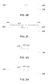
- FIGs. 2A-2H are diagrams detailing a product marking process according to an aspect of the invention.
- the product marking process shown in FIGs. 2A-2H pertains to one embodiment of the product marking process 100 illustrated in FIG. 1 .
- FIG. 2A is a diagram illustrating a housing portion 200.
- the housing portion 200 can represent a portion of a product housing, such as an outer housing of an electronic device.
- FIG. 2B is a diagram illustrating the housing portion 200 having a photoresist layer 202 applied thereon.
- FIG. 2C is a diagram illustrating a masking film 204 applied over the photoresist layer 202 on the housing portion 200.
- the masking film 204 includes opaque sections 206 and translucent sections 208.
- the translucent sections 208 can provide a predetermined pattern for marking of the product housing.
- FIG. 2D is a diagram illustrating the housing portion 200 after having been exposed to radiation.
- ultraviolet (UV) radiation can be directed at the photoresist layer 202 on the housing portion 200 through the masking film 204.
- the exposed photoresist layer 202' includes exposed photoresist regions 210 below the translucent sections 208 in the masking film 204.
- FIG. 2E is a diagram illustrating the housing portion 200 having the remaining photoresist layer 202".
- the remaining photoresist layer 202" results from removal of the masking film 204 and those regions 211 of the photoresist layer 202' that were activated by the exposure to radiation.
- FIG. 2F is a diagram illustrating the housing portion 200 after a layer of material 212 is applied over the remaining photoresist layer 202".
- the layer of material 212 is applied not only over the remaining portion of the photoresist layer 202" but also directly over the outer surface of the housing portion 200 where the photoresist layer 202 has been removed.
- the layer of material 212 can, for example, be applied through a sputtering technique, such as through Physical Vapor Deposition (PVD). Also, as an example, the layer of material can be a metal.
- FIG. 2G is a diagram illustrating the housing portion 200 after the remaining photoresist layer 202" is removed.
- the layer of material 212 applied over the remaining portion of the photoresist layer 202" is also removed.
- the portion of the layer of material 212' that remains is that portion that has been provided directly over the outer surface of the housing portion 200.
- FIG. 2H is a diagram illustrating the housing portion 200 after a protective coating 216 is applied on the outer surface of the housing portion 200 over the remaining portion of the layer of material 212'.
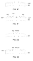
- FIGs. 3A-3H are diagrams detailing a product marking process according to another aspect of the invention.
- the product marking process shown in FIGs. 3A-3H pertains to one embodiment of the product marking process 100 illustrated in FIG. 1 .
- FIG. 3A is a diagram illustrating a housing portion 300.
- the housing portion 300 can represent a portion of a product housing, such as an outer housing of an electronic device.
- the housing portion 300 is curved. Marking is rendered more complicated when the surface to be marked has curvature.
- the product marking process according to the invention is suitable for use on flat, curved or complex surfaces.
- FIG. 3B is a diagram illustrating the housing portion 300 having a photoresist layer 302 applied thereon.
- FIG. 3C is a diagram illustrating a masking film 304 applied over the photoresist layer 302 on the housing portion 300.
- the masking film 304 includes opaque sections 306 and translucent sections 308.
- the translucent sections 308 can provide a predetermined pattern for marking of the product housing.
- FIG. 3D is a diagram illustrating the housing portion 300 after having been exposed to radiation.
- ultraviolet (UV) radiation can be directed at the photoresist layer 302 on the housing portion 300 through the masking film 304.
- the exposed photoresist layer 302' includes exposed photoresist regions 310 below the translucent sections 308 in the masking film 304.
- FIG. 3E is a diagram illustrating the housing portion 300 having the remaining photoresist layer 302".
- the remaining photoresist layer 302" results from removal of the masking film 304 and those regions 311 of the photoresist layer 302' that were activated by the exposure to radiation.
- FIG. 3F is a diagram illustrating the housing portion 300 after a layer of material 312 is applied over the remaining photoresist layer 302".
- the layer of material 312 is applied not only over the remaining portion of the photoresist layer 302" but also directly over the outer surface of the housing portion 300 where the photoresist layer 302 has been removed.
- the layer of material 312 can, for example, be applied through a sputtering technique, such as through Physical Vapor Deposition (PVD). Also, as an example, the layer of material can be a metal.
- FIG. 3G is a diagram illustrating the housing portion 300 after the remaining photoresist layer 302" is removed.
- the layer of material 312 applied over the remaining portion of the photoresist layer 302" is also removed.
- the portion of the layer of material 312' that remains is that portion that has been provided directly over the outer surface of the housing portion 300.
- FIG. 3H is a diagram illustrating the housing portion 300 after a protective coating 316 is applied on the outer surface of the housing portion 300 over the remaining portion of the layer of material 312'.
- a photolithographic mask is used, where a photoresist layer is adhered to an outer surface housing.
- a mask that performs a similar function can be formed from different techniques.
- a mask can be pad printed on the outer surface housing.
- a mask can be silk screened onto the outer surface housing.
- a mask can be printed, such as with an ink jet printing device, onto the outer surface housing.
- the method of the present invention described herein provides product marking using ablation.
- material that is to be used for marking is deposited onto a product surface and then selectively ablated to yield the text and/or graphics for the product marketing.
- FIG. 4 is a process flow diagram for a product marking process 400 according to the invention.
- the product marking process 400 can mark a housing of an electrical device.
- the product marking process 400 can be used to form text and/or graphics onto a housing surface, such as an outer housing surface, of an electrical device.
- the product marking process 410 initially forms 402 a physical mask layer having at least one predetermined opening.
- the predetermined opening is, for example, an opening that surrounds a region were text or graphics is to be applied to the outer housing surface. In other words, the predetermined opening is oversized as compared to the region where text or graphic is to be applied on the outer housing surface.
- the physical mask layer can be implemented by a film having at die cut for the predetermined opening. In the event that the physical mask layer has more than one predetermined opening, the physical mask layer can have a die cut for each of the predetermined openings.
- the physical mask layer can be adhered 404 to the outer housing surface.
- the physical mask layer can be adhered 404 to the outer housing surface through use of an adhesive.
- the physical mask can have an adhesive backing.
- a layer of material can be deposited 406 onto the outer housing surface.
- a deposition technique such as sputtering, can be used to deposit 406 a layer of material onto the outer housing surface.
- the deposition technique uses a Physical Vapor Deposition (PVD) process.
- the layer of material being deposited 406 is the material that is to form the marking.
- the layer of material can be a layer of metal, such as aluminum.
- the physical mask layer can be removed 408 from the outer housing surface.
- the product marking process 400 can ablate 410 away portions of the layer of material that are not desired.
- the ablation 410 can utilize a laser to precisely remove portions of the layer of material that has been deposited 406 onto the outer housing surface.
- the ablation 410 can thus form specific graphical elements and/or text elements into the layer of material by ablation 410 of those portions of the layer of material that are not needed to represent the desired graphical elements and/or textual elements that are to remain on the outer housing surface.
- the laser performing the ablation 410 is a YV04 laser (e.g., 1064 nanometer (NM)). Through proper control of the laser, the ablation 410 of undesired portion of the layer of material can be removed without damaging the surface of the outer surface housing.
- a translucent protective layer can be applied 412 to the outer housing surface.
- the translucent protective layer can serve to protect the remaining portion of the layer of material that is used to represent the one or more desired graphical elements and/or textual elements on the outer housing surface.
- the translucent protective layer can be a layer of acrylic.
- the use of a physical mask in the product marking process 400 is optional.
- the physical mask serves to confine the area(s) where ablation is to be performed.
- the product marking can be performed with simply operations 406 and 410 of the product marking process 400, though this entails additional ablation.
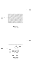
- FIGs. 5A-5E are diagrams detailing the product marking process according to the invention.
- the product marking process shown in FIGs. 5A-5D pertains to an embodiment of the product marking process 400 illustrated in FIG. 4 .
- FIG. 5A is a diagram illustrating a housing portion 500.
- the housing portion 500 can represent a portion of a product housing, such as an outer housing of an electronic device.
- a mask layer 502 is attached to the housing portion 500.
- the mask layer has at least one predetermined opening 503 that defines a region where marking of the outer housing is to be performed.
- FIG. 5B is a diagram illustrating the housing portion 500 having the mask layer 502 as well as a layer of material 504.
- the layer of material 504 is applied over the predetermined opening 503 in the mask layer 502 and may also be applied over some or all of the mask layer 502.
- FIG. 5C is a diagram illustrating the housing portion 500 having a remaining portion of the layer of material 504 that results after the mask layer 502 is removed from the housing portion 500.
- the remaining portion of the layer of material 504 corresponds to the predetermined pattern.
- FIG. 5D is a diagram illustrating the housing portion 500 after the remaining portion of the layer of material 504 is abated to remove unwanted areas. As shown in FIG. 5D , after the ablation, the layer of material 504 is now converted to specific marking elements 504'.
- the specific marking elements 504' can pertain to text and/or graphic elements that are formed from the layer of material 504 using laser ablation.
- FIG. 5E is a diagram illustrating the housing portion 500 after a protective coating 506 is applied on the outer surface of the housing portion 500 over the specific marking elements 504' that have been formed in the layer of material 504.
- FIGs. 6A and 6B are diagrams illustrating exemplary marking of a product in accordance with a product marking process, such as the product marking process shown in FIGs. 5A-5E or the product marking process 400 illustrated in FIG. 4 .
- FIG. 6A illustrates a product housing 600 according to one embodiment.
- the product housing 600 being illustrated can represent one surface, such as back surface, of a handheld electronic device.
- a predetermined region 602 of the illustrated surface can be coated or covered with a layer of material to be used for marking.
- a masking layer can be used to confine the layer of material to the predetermined region 602.
- FIG. 6B illustrates the product housing 600 after the layer of material in the predetermined region 602 has been ablated away to yield the desired labeling.
- the labeling includes a logo graphic 604, serial number 606, model number 608, and certification/approval marks 610 and 612.
- the product marking techniques discussed herein can be used to provide markings on a portable electronic device.
- the portable electronic device can further be a hand-held electronic device.
- the term hand-held generally means that the electronic device has a form factor that is small enough to be comfortably held in one hand.
- a hand-held electronic device may be directed at one-handed operation or two-handed operation. In one-handed operation, a single hand is used to both support the device as well as to perform operations with the user interface during use. In two-handed operation, one hand is used to support the device while the other hand performs operations with a user interface during use or alternatively both hands support the device as well as perform operations during use.
- the hand-held electronic device is sized for placement into a pocket of the user. By being pocket-sized, the user does not have to directly carry the device and therefore the device can be taken almost anywhere the user travels (e.g., the user is not limited by carrying a large, bulky and often heavy device).
- markings can be provided to product housings.
- the marking being provided can have a resolution whereby thirty (30) micron line widths can be achieved.
- the marking techniques are effective for surfaces that are flat or curved.
- the marking techniques have good adhesion characteristics to product housings, such as plastic housings.
- markings can be formed that are metallic and reflective for superior visual appearance.
- one or several markings can be provided to one or more distinct areas of a product's housing. The various markings can be efficiently provided in a sequential or concurrent manner.
Landscapes
- Engineering & Computer Science (AREA)
- Physics & Mathematics (AREA)
- General Physics & Mathematics (AREA)
- Manufacturing & Machinery (AREA)
- Microelectronics & Electronic Packaging (AREA)
- Casings For Electric Apparatus (AREA)
Description
- The present invention relates to marking products and, more particularly, marking outer housing surfaces of electronic devices.
- Consumer products, such as electronic devices, have been marked with different information for many years. For example, it is common for electronic devices to be marked with a serial number, model number, copyright information and the like. Conventionally, such marking is done with an ink printing or stamping process. Although conventional ink printing and stamping is useful for many situations, such techniques can be inadequate in the case of handheld electronic devices. The small form factor of handheld electronic devices, such as mobile phones, portable media players and Personal Digital Assistants (PDAs), requires that the marking be very small. In order for such small marking to be legible, the marking must be accurately and precisely formed. Unfortunately, however, conventional techniques are not able to offer sufficient accuracy and precision. Thus, there is a need for improved techniques to mark products.
-
EP 0031463 discloses a process for depositing a pattern of material on a semiconductor substrate. In this process a multi-layer lift-off mask is prepared using a polymer underlayer from a resist having a photo-active compound content. -
EP 0234121 discloses a method of printing a number of superimposed or otherwise geometrically related layers on a substrate with exact registration. The method involves printing the layers over one or more areas on the substrate so as to overlap the boundary of the areas, then removing the layers outside the areas. -
WO 2006/124279 discloses methods of making an article bearing a relief image using a removable film. An imageable film that contains at least a mask substrate and an imageable material is imagewise exposed to imaging radiation to form an imaged film. The imaged film is then transferred to an imageable article, such as a flexographic printing plate precursor. The resulting assembly is exposed to curing radiation resulting in exposed and unexposed areas of photosensitive material on the imageable article. -
US 2002/0097440 discloses a high definition photographic engraving procedure. - The invention pertains to a method for depositing material to selected regions of an electronic device housing according to claim 1 to provide markings on said housing. The markings provided on products can be textual and/or graphic. The method of the present invention can provide high resolution markings on surfaces that are flat or curved.
- The housing for a particular product can include an outer housing surface and the markings can be provided on the outer housing surface.
- In general, the markings, or annotations, provided on products according to the invention can be textual and/or graphic. The markings can be used to provide a product (e.g., a product's housing) with certain information. The marking can, for example, be use to label the product with various information. When a marking includes text, the text can provide information concerning the product (e.g., electronic device). For example, the text can include one or more of: name of product, trademark or copyright information, design location, assembly location, model number, serial number, license number, agency approvals, standards compliance, electronic codes, memory of device, and the like). When a marking includes a graphic, the graphic can pertain to a logo, a certification mark, standards mark or an approval mark that is often associated with the product. The marking can be used for advertisements to be provided on products. The markings can also be used for customization (e.g., user customization) of a housing of a product.
- One aspect described herein provides product marking using photolithography. Here, intermediate material can be adhered to a product surface, then patterned, and then material that is to be used for marking can deposited onto the product surface. Subsequently, any remaining intermediate material can be removed (along with any intermediate material) such that the product thereafter includes the text and/or graphics for the product marketing
- Another aspect of the method according to the invention provides product marking using laser ablation. Here, material that is to be used for marking is deposited onto a product surface and then ablated to yield the text and/or graphics for the product marketing.
- The method for depositing material to selected regions of an electronic device housing according to the invention the invention includes forming a mask layer having at least one predetermined pattern; adhering the mask layer to a housing surface of the electronic device housing; depositing a layer of material onto the housing surface, the layer of material being provided on the housing surface at least within the predetermined opening of the mask layer; subsequently removing the mask layer from the housing surface, thereby retaining the layer of material on the housing surface in accordance with the predetermined pattern; and removing select portions of the layer of material that are not desired to remain on the housing surface, wherein said removing of the select portions of the layer of material comprises performing laser ablation of select portions of the layer of material on the housing surface to thereby remove the select portions of the of the layer of material that are not desired to remain on the outer surface housing.
- Other aspects and advantages of the invention will become apparent from the following detailed description taken in conjunction with the accompanying drawings which illustrate, by way of example, the principles of the invention.
- The invention will be readily understood by the following detailed description in conjunction with the accompanying drawings, wherein like reference numerals designate like structural elements, and in which:
-
FIG. 1 is a process flow diagram for product marking process according to an embodiment of the invention. -
FIGs. 2A-2H are diagrams detailing a product marking process according to an embodiment of the invention. -
FIGs. 3A-3H are diagrams detailing a product marking process according to an embodiment of the invention. -
FIG. 4 is a process flow diagram for a product marking process according the invention. -
FIGs. 5A-5E are diagrams detailing a product marking process according to an embodiment of the invention. -
FIGs. 6A and 6B are diagrams illustrating exemplary marking of a product in accordance with the product marking process of the invention. - The invention pertains to a method for providing markings on electronic device housing products. The markings provided on products can be textual and/or graphic. The method can provide high resolution markings on surfaces that are flat or curved. In one embodiment, the products have housings and the markings are to be provided on the housings. For example, the housing for a particular product can include an outer housing surface and the markings can be provided on the outer housing surface.
- In general, the markings, or annotations, provided on products according to the invention can be textual and/or graphic. The markings can be used to provide a product (e.g., a product's housing) with certain information. The marking can, for example, be use to label the product with various information. When a marking includes text, the text can provide information concerning the product (e.g., electronic device). For example, the text can include one or more of: name of product, trademark or copyright information, design location, assembly location, model number, serial number, license number, agency approvals, standards compliance, electronic codes, memory of device, and the like). When a marking includes a graphic, the graphic can pertain to a logo, a certification mark, standards mark or an approval mark that is often associated with the product. The marking can be used for advertisements to be provided on products. The markings can also be used for customization (e.g., user customization) of a housing of a product.
- Embodiments of the invention are discussed below with reference to
FIGs. 1 - 6B . However, those skilled in the art will readily appreciate that the detailed description given herein with respect to these figures is for explanatory purposes as the invention extends beyond these limited embodiments. - One aspect described herein provides product marking using photolithography. Here, an intermediate material can be adhered to a product surface, then patterned, and then material that is to be used for marking can deposited onto the product surface. Subsequently, any remaining intermediate material can be removed (along with any of the material used for marking that is provided therein) such that the product thereafter includes the text and/or graphics for the product marketing in accordance with the patterned intermediate material.
-
FIG. 1 is a process flow diagram forproduct marking process 100 according to an aspect of the invention. Theproduct marking process 100 is, for example, suitable for applying text or graphics to a housing surface (e.g., an outer housing surface) of an electronic device. Theproduct marking process 100 is, in one embodiment, particularly well-suited for applying text and/or graphics to an outer housing surface of a handheld electronic device. Examples of handheld electronic devices include mobile telephones (e.g., cell phones), Personal Digital Assistants (PDAs), portable media players, remote controllers, pointing devices (e.g., computer mouse), game controllers, etc. - The
product marking process 100 operates to mark an outer housing surface of an electronic device. Theproduct marking process 100 is a multi-step process to form high resolution text or graphics onto the outer housing surface. The outer housing surface can be flat or curved. - Initially, the
product marking process 100 adheres 102 a photoresist layer to an outer housing surface. In effect, the photoresist layer is laminated against the outer housing surface (since the outer housing surface is to carry the marking). In one implementation, to ensure that the photoresist layer is tightly sealed against the outer housing surface (at least in the area being processed), one or more heated, conformable rollers can be used to apply heat and pressure. The conformable nature of the one or more roller is advantageous when the outer housing surface is curved. In this embodiment, the masking film can be a dry film photoresist. In an alternative embodiment, the masking film can be a wet film photoresist, which can be positioned 104 on the photoresist layer using spin-coating. - Next, a masking film can be positioned 104 over the photoresist layer on the outer housing surface. The masking film and the photoresist later can then be exposed 106 to radiation. For example, the radiation can be ultraviolet (UV) radiation that is used to activate portions of the photoresist layer. More particularly, the masking film has a predetermined pattern for the text or graphics to be applied to the outer housing surface. Hence, by applying the masking film over at the photoresist layer, only selected portions of the photoresist layer are activated by the radiation. In other words, the masking film allows the radiation to pass through to activate the photoresist layer in only the selected portions which pertain to the predetermined pattern. For example, the predetermined pattern of the masking film can be considered an inverse stencil in that is serves to block the radiation in regions where marking is not to be provided. In one implementation, the masking film can be a silver-halide thin film.
- Next, the masking film can be removed 108. Further, an exposed (i.e., activated) portion of the photoresist layer can be removed 110. The removal of the photoresist layer by performed by a chemical washing operation. In one implementation, the chemical washing can use a potassium carbonate or sodium carbonate solution.
- Thereafter, a layer of material can be deposited 112 onto the outer housing surface. For example, the layer of material can be deposited 112 by a deposition process, such as sputtering. One suitable process for the deposition of the layer of material is a Physical Vapor Deposition (PVD) process. The layer of material being deposited can very depending upon application. However, one suitable layer of material is a layer of metal, such as silver. Alternatively, the layer of material can be a layer of tin or other material that can be applied with a deposition process.
- Next, any remaining photoresist can be removed 114 from the outer housing surface. The layer of material that is deposited on the remaining photoresist is also removed as the underlying photoresist is removed. The removal of the photoresist layer by performed by a chemical washing operation. In one implementation, the chemical washing can use a relatively weak solution of sodium hydroxide (NaOH).
- Thereafter, if desired, a translucent protective layer can be applied 116 to the outer housing surface so as to cover and protect the remaining layer of material that provides the graphical elements and/or textual elements on the outer housing surface that serve to mark the product. For example, the translucent protective layer can be a layer of acrylic. Following the
block 116, theproduct marking process 100 can end. - In one embodiment, at least a portion of product housing can be formed of a plastic or resin, such as polycarbonate. The marking can use a material that is metal (e.g., silver), which can be reflective. The resulting marking on the product housing is thus able to be provided in high resolution on a product's housing.
- In one particular embodiment, the processing parameters for one suitable implementation can, for example, be as follows:
-
- Lamination speed: 53 rpm
- Laminating temp: 100 degrees Celsius
- Lamination pressure: 5 Kg/cm2
- Roller hardness: ≤ 68
- Pressure uniformity
- Roller cleaning (with Isopropyl Alcohol), e.g., to prevent press in dents
-
- Exposure Energy: 78 mj/cm2
- Resist: 1 (e.g., in case of a white housing)
- Main vacuum: <-700 KPa
- Phototool Dmax: > 4.5
- Phototool: No Emulsion Protective Layer
- Exposure vacuum foil: Using clear film Polyethylene Teraphthalate (PET)
- Change white light to yellow light
- Avoid scratch and cleaning tray
- Avoid paint and protect rustiness using tape
- Cleaning and stick roller
-
- Sodium carbonate: 0.8%~0.9%
- Break point: 50%-60%
- Pressure: 1.8 Kg/cm2
- Speed: 4.7 m/min (3 dev chamber)
- Hard Water rinse: 200-250 ppm
- Rinse (e.g., de-ionized water rinse
-
- Sodium hydroxide: 1.5%
- Solution temperature: 50 degrees Celsius
- Stripping time: 5'40"~6'
- Stripping time can be reduced with other solutions
-
FIGs. 2A-2H are diagrams detailing a product marking process according to an aspect of the invention. The product marking process shown inFIGs. 2A-2H pertains to one embodiment of theproduct marking process 100 illustrated inFIG. 1 . -
FIG. 2A is a diagram illustrating ahousing portion 200. Thehousing portion 200 can represent a portion of a product housing, such as an outer housing of an electronic device. -
FIG. 2B is a diagram illustrating thehousing portion 200 having aphotoresist layer 202 applied thereon. -
FIG. 2C is a diagram illustrating amasking film 204 applied over thephotoresist layer 202 on thehousing portion 200. Themasking film 204 includesopaque sections 206 andtranslucent sections 208. Thetranslucent sections 208 can provide a predetermined pattern for marking of the product housing. -
FIG. 2D is a diagram illustrating thehousing portion 200 after having been exposed to radiation. For example, ultraviolet (UV) radiation can be directed at thephotoresist layer 202 on thehousing portion 200 through themasking film 204. As a result, the exposed photoresist layer 202' includes exposedphotoresist regions 210 below thetranslucent sections 208 in themasking film 204. -
FIG. 2E is a diagram illustrating thehousing portion 200 having the remainingphotoresist layer 202". Here, the remainingphotoresist layer 202" results from removal of themasking film 204 and those regions 211 of the photoresist layer 202' that were activated by the exposure to radiation. -
FIG. 2F is a diagram illustrating thehousing portion 200 after a layer ofmaterial 212 is applied over the remainingphotoresist layer 202". The layer ofmaterial 212 is applied not only over the remaining portion of thephotoresist layer 202" but also directly over the outer surface of thehousing portion 200 where thephotoresist layer 202 has been removed. The layer ofmaterial 212 can, for example, be applied through a sputtering technique, such as through Physical Vapor Deposition (PVD). Also, as an example, the layer of material can be a metal. -
FIG. 2G is a diagram illustrating thehousing portion 200 after the remainingphotoresist layer 202" is removed. Here, the layer ofmaterial 212 applied over the remaining portion of thephotoresist layer 202" is also removed. However, the portion of the layer ofmaterial 212' that remains is that portion that has been provided directly over the outer surface of thehousing portion 200. -
FIG. 2H is a diagram illustrating thehousing portion 200 after aprotective coating 216 is applied on the outer surface of thehousing portion 200 over the remaining portion of the layer ofmaterial 212'. -
FIGs. 3A-3H are diagrams detailing a product marking process according to another aspect of the invention. The product marking process shown inFIGs. 3A-3H pertains to one embodiment of theproduct marking process 100 illustrated inFIG. 1 . -
FIG. 3A is a diagram illustrating ahousing portion 300. Thehousing portion 300 can represent a portion of a product housing, such as an outer housing of an electronic device. In this embodiment, thehousing portion 300 is curved. Marking is rendered more complicated when the surface to be marked has curvature. However, the product marking process according to the invention is suitable for use on flat, curved or complex surfaces. -
FIG. 3B is a diagram illustrating thehousing portion 300 having aphotoresist layer 302 applied thereon. -
FIG. 3C is a diagram illustrating amasking film 304 applied over thephotoresist layer 302 on thehousing portion 300. Themasking film 304 includesopaque sections 306 andtranslucent sections 308. Thetranslucent sections 308 can provide a predetermined pattern for marking of the product housing. -
FIG. 3D is a diagram illustrating thehousing portion 300 after having been exposed to radiation. For example, ultraviolet (UV) radiation can be directed at thephotoresist layer 302 on thehousing portion 300 through themasking film 304. As a result, the exposed photoresist layer 302' includes exposedphotoresist regions 310 below thetranslucent sections 308 in themasking film 304. -
FIG. 3E is a diagram illustrating thehousing portion 300 having the remainingphotoresist layer 302". Here, the remainingphotoresist layer 302" results from removal of themasking film 304 and those regions 311 of the photoresist layer 302' that were activated by the exposure to radiation. -
FIG. 3F is a diagram illustrating thehousing portion 300 after a layer ofmaterial 312 is applied over the remainingphotoresist layer 302". The layer ofmaterial 312 is applied not only over the remaining portion of thephotoresist layer 302" but also directly over the outer surface of thehousing portion 300 where thephotoresist layer 302 has been removed. The layer ofmaterial 312 can, for example, be applied through a sputtering technique, such as through Physical Vapor Deposition (PVD). Also, as an example, the layer of material can be a metal. -
FIG. 3G is a diagram illustrating thehousing portion 300 after the remainingphotoresist layer 302" is removed. Here, the layer ofmaterial 312 applied over the remaining portion of thephotoresist layer 302" is also removed. However, the portion of the layer of material 312' that remains is that portion that has been provided directly over the outer surface of thehousing portion 300. -
FIG. 3H is a diagram illustrating thehousing portion 300 after aprotective coating 316 is applied on the outer surface of thehousing portion 300 over the remaining portion of the layer of material 312'. - In the
product marking process 100 illustrated inFIG. 1 , a photolithographic mask is used, where a photoresist layer is adhered to an outer surface housing. However, in other embodiment, a mask that performs a similar function can be formed from different techniques. As one example, a mask can be pad printed on the outer surface housing. As another example, a mask can be silk screened onto the outer surface housing. As still another example, a mask can be printed, such as with an ink jet printing device, onto the outer surface housing. - The method of the present invention described herein provides product marking using ablation. Here, material that is to be used for marking is deposited onto a product surface and then selectively ablated to yield the text and/or graphics for the product marketing.
-
FIG. 4 is a process flow diagram for aproduct marking process 400 according to the invention. In this embodiment, theproduct marking process 400 can mark a housing of an electrical device. For example, theproduct marking process 400 can be used to form text and/or graphics onto a housing surface, such as an outer housing surface, of an electrical device. - The
product marking process 410 initially forms 402 a physical mask layer having at least one predetermined opening. The predetermined opening is, for example, an opening that surrounds a region were text or graphics is to be applied to the outer housing surface. In other words, the predetermined opening is oversized as compared to the region where text or graphic is to be applied on the outer housing surface. The physical mask layer can be implemented by a film having at die cut for the predetermined opening. In the event that the physical mask layer has more than one predetermined opening, the physical mask layer can have a die cut for each of the predetermined openings. - After the physical mask has been formed 402, the physical mask layer can be adhered 404 to the outer housing surface. In one implementation, the physical mask layer can be adhered 404 to the outer housing surface through use of an adhesive. For example, the physical mask can have an adhesive backing.
- Next, a layer of material can be deposited 406 onto the outer housing surface. For example, a deposition technique, such as sputtering, can be used to deposit 406 a layer of material onto the outer housing surface. In one implementation, the deposition technique uses a Physical Vapor Deposition (PVD) process. The layer of material being deposited 406 is the material that is to form the marking. For example, the layer of material can be a layer of metal, such as aluminum. Thereafter, the physical mask layer can be removed 408 from the outer housing surface.
- After the physical mask layer has been removed 408, the
product marking process 400 can ablate 410 away portions of the layer of material that are not desired. Theablation 410 can utilize a laser to precisely remove portions of the layer of material that has been deposited 406 onto the outer housing surface. Theablation 410 can thus form specific graphical elements and/or text elements into the layer of material byablation 410 of those portions of the layer of material that are not needed to represent the desired graphical elements and/or textual elements that are to remain on the outer housing surface. In one implementation, the laser performing theablation 410 is a YV04 laser (e.g., 1064 nanometer (NM)). Through proper control of the laser, theablation 410 of undesired portion of the layer of material can be removed without damaging the surface of the outer surface housing. - Subsequently, a translucent protective layer can be applied 412 to the outer housing surface. Although the translucent protective layer is not required, the translucent protective layer can serve to protect the remaining portion of the layer of material that is used to represent the one or more desired graphical elements and/or textual elements on the outer housing surface. For example, the translucent protective layer can be a layer of acrylic. Following the
block 412, theproduct marking process 400 can end. - It should be noted that the use of a physical mask in the
product marking process 400 is optional. The physical mask serves to confine the area(s) where ablation is to be performed. Hence, in one embodiment, the product marking can be performed with simplyoperations product marking process 400, though this entails additional ablation. -
FIGs. 5A-5E are diagrams detailing the product marking process according to the invention. The product marking process shown inFIGs. 5A-5D pertains to an embodiment of theproduct marking process 400 illustrated inFIG. 4 . -
FIG. 5A is a diagram illustrating ahousing portion 500. Thehousing portion 500 can represent a portion of a product housing, such as an outer housing of an electronic device. Amask layer 502 is attached to thehousing portion 500. The mask layer has at least onepredetermined opening 503 that defines a region where marking of the outer housing is to be performed. -
FIG. 5B is a diagram illustrating thehousing portion 500 having themask layer 502 as well as a layer ofmaterial 504. The layer ofmaterial 504 is applied over thepredetermined opening 503 in themask layer 502 and may also be applied over some or all of themask layer 502. -
FIG. 5C is a diagram illustrating thehousing portion 500 having a remaining portion of the layer ofmaterial 504 that results after themask layer 502 is removed from thehousing portion 500. The remaining portion of the layer ofmaterial 504 corresponds to the predetermined pattern. -
FIG. 5D is a diagram illustrating thehousing portion 500 after the remaining portion of the layer ofmaterial 504 is abated to remove unwanted areas. As shown inFIG. 5D , after the ablation, the layer ofmaterial 504 is now converted tospecific marking elements 504'. Thespecific marking elements 504' can pertain to text and/or graphic elements that are formed from the layer ofmaterial 504 using laser ablation. -
FIG. 5E is a diagram illustrating thehousing portion 500 after aprotective coating 506 is applied on the outer surface of thehousing portion 500 over thespecific marking elements 504' that have been formed in the layer ofmaterial 504. -
FIGs. 6A and 6B are diagrams illustrating exemplary marking of a product in accordance with a product marking process, such as the product marking process shown inFIGs. 5A-5E or theproduct marking process 400 illustrated inFIG. 4 . -
FIG. 6A illustrates aproduct housing 600 according to one embodiment. Theproduct housing 600 being illustrated can represent one surface, such as back surface, of a handheld electronic device. Apredetermined region 602 of the illustrated surface can be coated or covered with a layer of material to be used for marking. As noted above, a masking layer can be used to confine the layer of material to thepredetermined region 602. -
FIG. 6B illustrates theproduct housing 600 after the layer of material in thepredetermined region 602 has been ablated away to yield the desired labeling. In this example, the labeling includes a logo graphic 604,serial number 606,model number 608, and certification/approval marks 610 and 612. - In one embodiment, the product marking techniques discussed herein can be used to provide markings on a portable electronic device. The portable electronic device can further be a hand-held electronic device. The term hand-held generally means that the electronic device has a form factor that is small enough to be comfortably held in one hand. A hand-held electronic device may be directed at one-handed operation or two-handed operation. In one-handed operation, a single hand is used to both support the device as well as to perform operations with the user interface during use. In two-handed operation, one hand is used to support the device while the other hand performs operations with a user interface during use or alternatively both hands support the device as well as perform operations during use. In some cases, the hand-held electronic device is sized for placement into a pocket of the user. By being pocket-sized, the user does not have to directly carry the device and therefore the device can be taken almost anywhere the user travels (e.g., the user is not limited by carrying a large, bulky and often heavy device).
- Additional information on product marking as well as other manufacturing techniques and systems for electronic devices are contained in
U.S. Provisional Patent Application No. 61/059,789, filed June 8, 2008 - The various aspects, features, embodiments or implementations of the invention described above can be used alone or in various combinations.
- Different aspects, embodiments or implementations may, but need not, yield one or more of the following advantages. One advantage is that high precision markings can be provided to product housings. As an example, the marking being provided can have a resolution whereby thirty (30) micron line widths can be achieved. Another advantage is that the marking techniques are effective for surfaces that are flat or curved. Another advantage is that the marking techniques have good adhesion characteristics to product housings, such as plastic housings. Still another advantage is that markings can be formed that are metallic and reflective for superior visual appearance. Yet still another advantage is that one or several markings can be provided to one or more distinct areas of a product's housing. The various markings can be efficiently provided in a sequential or concurrent manner.
- The many features and advantages of the present invention are apparent from the written description. Further, since numerous modifications and changes will readily occur to those skilled in the art, the invention should not be limited to the exact construction and operation as illustrated and described. Hence, all suitable modifications and equivalents may be resorted to as falling within the scope of the invention.
Claims (13)
- A method for depositing material to selected regions of an electronic device housing, said method comprising:forming a mask layer having at least one predetermined opening in a predetermined pattern;adhering the mask layer to a housing surface of the electronic device housing;depositing a layer of material onto the housing surface, the layer of material being provided on the housing surface at least within the or each predetermined opening of the mask layer; andsubsequently removing the mask layer from the housing surface, thereby retaining the layer of material on the housing surface in accordance with the predetermined pattern; andremoving select portions of the layer of material that are not desired to remain on the housing surface, wherein said removing of the select portions of the layer of material comprises performing laser ablation of the select portions of the layer of material on the housing surface to thereby remove the select portions of the layer of material that are not desired to remain on the housing surface.
- A method as recited in claim 1, wherein said method further comprises:subsequently applying a translucent protective layer to the housing surface so as to cover at least the remaining portions of the layer of material that remain on the housing surface.
- A method as recited in claim 1 or claim 2, wherein the remaining portions of the layer of material retained on the housing surface include text and graphics.
- A method as recited in claim 1 or claim 2, wherein the remaining portions of the layer of material retained on the housing surface include at least one graphic, the at least one graphic being a logo, a certification mark or an approval mark.
- A method as recited in claim 1 or claim 2, wherein the or each predetermined opening is oversized as compared to an area for the remaining portions of the layer of materials that remain on the housing surface.
- A method as recited in any of the preceding claims, wherein the layer of material is a layer of metal.
- A method as recited in claim 6, wherein the layer of metal is a layer of aluminum.
- A method as recited in any of the preceding claims, wherein the electronic device housing is for a handheld, portable electronic device.
- A method as recited in any of the preceding claims, wherein the housing surface is an outer housing surface.
- A method as recited in any of the preceding claims, wherein the mask layer is formed of photoresist.
- A method as recited in any of the preceding claims, wherein said forming of the mask layer comprises ink jet printing the mask layer onto the housing surface.
- A method as recited in any of claims 1 to 10, wherein said forming of the mask layer comprises pad printing the mask layer onto the housing surface.
- A method as recited in any of claims 1 to 10, wherein said forming of the mask layer comprises silk screening the mask layer onto the housing surface.
Applications Claiming Priority (3)
| Application Number | Priority Date | Filing Date | Title |
|---|---|---|---|
| US12149108P | 2008-12-10 | 2008-12-10 | |
| US12/475,597 US8367304B2 (en) | 2008-06-08 | 2009-05-31 | Techniques for marking product housings |
| EP09802048.0A EP2356520B1 (en) | 2008-12-10 | 2009-10-23 | Technique for marking product housings |
Related Parent Applications (2)
| Application Number | Title | Priority Date | Filing Date |
|---|---|---|---|
| EP09802048.0A Division EP2356520B1 (en) | 2008-12-10 | 2009-10-23 | Technique for marking product housings |
| EP09802048.0A Division-Into EP2356520B1 (en) | 2008-12-10 | 2009-10-23 | Technique for marking product housings |
Publications (2)
| Publication Number | Publication Date |
|---|---|
| EP2752713A1 EP2752713A1 (en) | 2014-07-09 |
| EP2752713B1 true EP2752713B1 (en) | 2016-10-05 |
Family
ID=41785629
Family Applications (2)
| Application Number | Title | Priority Date | Filing Date |
|---|---|---|---|
| EP14162918.8A Not-in-force EP2752713B1 (en) | 2008-12-10 | 2009-10-23 | Techniques for marking product housings |
| EP09802048.0A Not-in-force EP2356520B1 (en) | 2008-12-10 | 2009-10-23 | Technique for marking product housings |
Family Applications After (1)
| Application Number | Title | Priority Date | Filing Date |
|---|---|---|---|
| EP09802048.0A Not-in-force EP2356520B1 (en) | 2008-12-10 | 2009-10-23 | Technique for marking product housings |
Country Status (4)
| Country | Link |
|---|---|
| US (2) | US8367304B2 (en) |
| EP (2) | EP2752713B1 (en) |
| CN (2) | CN102246097B (en) |
| WO (1) | WO2010068340A2 (en) |
Families Citing this family (29)
| Publication number | Priority date | Publication date | Assignee | Title |
|---|---|---|---|---|
| US8192815B2 (en) | 2007-07-13 | 2012-06-05 | Apple Inc. | Methods and systems for forming a dual layer housing |
| US8315043B2 (en) * | 2008-01-24 | 2012-11-20 | Apple Inc. | Methods and systems for forming housings from multi-layer materials |
| US8646637B2 (en) * | 2008-04-18 | 2014-02-11 | Apple Inc. | Perforated substrates for forming housings |
| US8367304B2 (en) | 2008-06-08 | 2013-02-05 | Apple Inc. | Techniques for marking product housings |
| US20100159273A1 (en) | 2008-12-24 | 2010-06-24 | John Benjamin Filson | Method and Apparatus for Forming a Layered Metal Structure with an Anodized Surface |
| US9173336B2 (en) | 2009-05-19 | 2015-10-27 | Apple Inc. | Techniques for marking product housings |
| US9884342B2 (en) | 2009-05-19 | 2018-02-06 | Apple Inc. | Techniques for marking product housings |
| US8663806B2 (en) * | 2009-08-25 | 2014-03-04 | Apple Inc. | Techniques for marking a substrate using a physical vapor deposition material |
| US8809733B2 (en) | 2009-10-16 | 2014-08-19 | Apple Inc. | Sub-surface marking of product housings |
| US20110089039A1 (en) * | 2009-10-16 | 2011-04-21 | Michael Nashner | Sub-Surface Marking of Product Housings |
| US9845546B2 (en) | 2009-10-16 | 2017-12-19 | Apple Inc. | Sub-surface marking of product housings |
| US10071583B2 (en) | 2009-10-16 | 2018-09-11 | Apple Inc. | Marking of product housings |
| US8628836B2 (en) | 2010-03-02 | 2014-01-14 | Apple Inc. | Method and apparatus for bonding metals and composites |
| US8489158B2 (en) | 2010-04-19 | 2013-07-16 | Apple Inc. | Techniques for marking translucent product housings |
| EP2563600B2 (en) * | 2010-04-30 | 2018-07-25 | Becton Dickinson France | Method for marking a transparent container |
| US8724285B2 (en) | 2010-09-30 | 2014-05-13 | Apple Inc. | Cosmetic conductive laser etching |
| CN102724840B (en) * | 2011-03-29 | 2015-03-04 | 富准精密工业(深圳)有限公司 | Shell and method for manufacturing the same |
| US20120248001A1 (en) | 2011-03-29 | 2012-10-04 | Nashner Michael S | Marking of Fabric Carrying Case for Portable Electronic Device |
| US9280183B2 (en) | 2011-04-01 | 2016-03-08 | Apple Inc. | Advanced techniques for bonding metal to plastic |
| US20130075126A1 (en) * | 2011-09-27 | 2013-03-28 | Michael S. Nashner | Laser Bleached Marking of Dyed Anodization |
| US8879266B2 (en) | 2012-05-24 | 2014-11-04 | Apple Inc. | Thin multi-layered structures providing rigidity and conductivity |
| US10071584B2 (en) | 2012-07-09 | 2018-09-11 | Apple Inc. | Process for creating sub-surface marking on plastic parts |
| US9477152B2 (en) * | 2012-09-27 | 2016-10-25 | E I Du Pont De Nemours And Company | Printing form precursor having indicia and a method for preparing a printing form from the precursor |
| US9314871B2 (en) | 2013-06-18 | 2016-04-19 | Apple Inc. | Method for laser engraved reflective surface structures |
| US9434197B2 (en) | 2013-06-18 | 2016-09-06 | Apple Inc. | Laser engraved reflective surface structures |
| KR20180050452A (en) * | 2016-11-04 | 2018-05-15 | 코닝 인코포레이티드 | Masking and fixturing of a glass-based article during a coating process and articles produced thereby |
| IL288650B2 (en) * | 2018-06-02 | 2025-09-01 | Scarselli Bruno | Asset identification, registration, tracking and commercialization apparatuses and methods |
| US10999917B2 (en) | 2018-09-20 | 2021-05-04 | Apple Inc. | Sparse laser etch anodized surface for cosmetic grounding |
| US12324114B2 (en) | 2021-09-24 | 2025-06-03 | Apple Inc. | Laser-marked electronic device housings |
Family Cites Families (169)
| Publication number | Priority date | Publication date | Assignee | Title |
|---|---|---|---|---|
| US2647079A (en) * | 1948-06-03 | 1953-07-28 | Sprague Electric Co | Production of insulated condenser electrodes |
| FR1127323A (en) | 1954-07-13 | 1956-12-13 | Daimler Benz Ag | Fixing device for construction elements made of artificial materials |
| US2812295A (en) | 1955-03-22 | 1957-11-05 | Gen Motors Corp | Method of finishing metal surfaces |
| US2990304A (en) | 1957-07-10 | 1961-06-27 | Reynolds Metals Co | Method of coloring aluminum surface |
| US3216866A (en) | 1961-03-06 | 1965-11-09 | Allied Decals Inc | Treatment of anodized aluminum |
| US3526694A (en) * | 1968-02-06 | 1970-09-01 | Jerome H Lemelson | Molding techniques |
| USRE28225E (en) | 1968-10-09 | 1974-11-05 | Photobleachable dye compositions | |
| US3615432A (en) | 1968-10-09 | 1971-10-26 | Eastman Kodak Co | Energy-sensitive systems |
| US3645777A (en) | 1970-09-04 | 1972-02-29 | Brudenell Corp The | Process of coating glass with durable coatings and resulting products |
| US4269947A (en) * | 1977-07-05 | 1981-05-26 | Teijin Limited | Cured or uncured aromatic polyester composition and process for its production |
| US4247600A (en) | 1978-07-28 | 1981-01-27 | Minolta Camera Kabushiki Kaisha | Metallized plastic camera housing and method |
| US4347428A (en) | 1979-08-27 | 1982-08-31 | Rowenta-Werke Gmbh | Handle and supporting structure for an electric pressing iron having electronic temperature control |
| EP0031463B1 (en) * | 1979-12-26 | 1984-06-13 | International Business Machines Corporation | Process for depositing a pattern of material on a substrate and use of this process for forming a patterned mask structure on a semiconductor substrate |
| JPS595678B2 (en) | 1981-03-09 | 1984-02-06 | 立山アルミニウム工業株式会社 | Pattern coloring method for aluminum or aluminum alloy |
| EP0114565A1 (en) | 1983-01-25 | 1984-08-01 | W. Bloesch Ag | Method of making a decoration on a glass, case or dial of a measuring instrument |
| US4547649A (en) * | 1983-03-04 | 1985-10-15 | The Babcock & Wilcox Company | Method for superficial marking of zirconium and certain other metals |
| DE3311882A1 (en) | 1983-03-31 | 1985-02-07 | Carl Baasel Lasertechnik GmbH, 8000 München | MATERIAL PIECE OF ALUMINUM, PREFERABLY ALUMINUM SHIELD AND METHOD FOR PRODUCING THE SAME |
| JPS6046213A (en) * | 1983-04-22 | 1985-03-13 | Takeo Nakagawa | Mold for vacuum molding and manufacture thereof |
| JPS603693U (en) * | 1983-06-20 | 1985-01-11 | 株式会社日本アルミ | Pot for induction cooker |
| US4686352B1 (en) | 1984-04-27 | 1993-12-14 | Sunbeam Corporation | Electronic pressing iron |
| DE3500079A1 (en) | 1985-01-03 | 1986-07-10 | Henkel KGaA, 4000 Düsseldorf | AGENT AND METHOD FOR PRODUCING COLORLESS COMPRESSION LAYERS ON ANODIZED ALUMINUM SURFACES |
| US4651453A (en) | 1985-11-18 | 1987-03-24 | Conair Corporation | Travel iron having controlled heat and compact storage |
| GB8531804D0 (en) * | 1985-12-24 | 1986-02-05 | Campbell P L | Printing |
| US4993148A (en) * | 1987-05-19 | 1991-02-19 | Mitsubishi Denki Kabushiki Kaisha | Method of manufacturing a circuit board |
| US4931366A (en) | 1988-07-14 | 1990-06-05 | The Stanley Works | Coated article with metallic appearance |
| JP2768509B2 (en) | 1989-10-24 | 1998-06-25 | 日本特許管理株式会社 | Manufacturing method of packaging material |
| JP2925121B2 (en) | 1989-12-29 | 1999-07-28 | ティーディーケイ株式会社 | Optical recording medium and optical recording method |
| US5417905A (en) * | 1989-05-26 | 1995-05-23 | Esec (Far East) Limited | Method of making a card having decorations on both faces |
| JPH0313331A (en) | 1989-06-10 | 1991-01-22 | Sumitomo Special Metals Co Ltd | Composite material variable in coefficient of thermal expansion and heat conductivity |
| US5224197A (en) | 1990-09-06 | 1993-06-29 | The United States Of America As Represented By The Secretary Of The Air Force | Integrated optics using photodarkened polystyrene |
| US5215864A (en) | 1990-09-28 | 1993-06-01 | Laser Color Marking, Incorporated | Method and apparatus for multi-color laser engraving |
| JPH06126192A (en) | 1991-02-04 | 1994-05-10 | Nippon Yakin Kogyo Co Ltd | Method for producing metal foil coated with oxide |
| US5196376A (en) * | 1991-03-01 | 1993-03-23 | Polycon Corporation | Laser lithography for integrated circuit and integrated circuit interconnect manufacture |
| JPH06212451A (en) | 1993-01-11 | 1994-08-02 | Osaka Prefecture | Metal surface decoration processing method |
| US5288344A (en) | 1993-04-07 | 1994-02-22 | California Institute Of Technology | Berylllium bearing amorphous metallic alloys formed by low cooling rates |
| JPH06320104A (en) | 1993-05-14 | 1994-11-22 | Shiyuunan Chiiki Jiba Sangyo Shinko Center | Method of manufacturing crafts with different color patterns |
| EP0633585B1 (en) | 1993-07-08 | 1997-11-05 | Philips Patentverwaltung GmbH | Housing for electric communication apparatus |
| US5645964A (en) | 1993-08-05 | 1997-07-08 | Kimberly-Clark Corporation | Digital information recording media and method of using same |
| JPH07204871A (en) | 1994-01-20 | 1995-08-08 | Fuji Electric Co Ltd | Marking method |
| US5560845A (en) | 1994-02-28 | 1996-10-01 | E. I. Du Pont De Nemours And Company | Laser marking of fluoropolymer composition |
| SE504039C2 (en) * | 1994-06-14 | 1996-10-21 | Ericsson Telefon Ab L M | Way to injection mold plastic |
| TW358215B (en) * | 1994-08-08 | 1999-05-11 | Thomson Consumer Electronics | Coded marking on an interior surface of a CRT faceplate panel and method of marking same |
| BE1008961A3 (en) | 1994-11-14 | 1996-10-01 | Philips Electronics Nv | IRON WITH SLIDE LAYER. |
| US5874133A (en) | 1995-06-07 | 1999-02-23 | Randemo, Inc. | Process for making a polyurethane composite |
| DE19523112C2 (en) | 1995-06-26 | 2003-09-18 | Daimler Chrysler Ag | Body component, in particular vehicle door or hood, and a method for producing the same |
| JPH0944269A (en) * | 1995-07-25 | 1997-02-14 | Fujitsu Ltd | Electronic device, housing for electronic device, and method for manufacturing housing |
| GB9521978D0 (en) | 1995-10-26 | 1996-01-03 | Sgs Thomson Microelectronics | Computer instruction supply |
| US5808268A (en) | 1996-07-23 | 1998-09-15 | International Business Machines Corporation | Method for marking substrates |
| US5719379A (en) | 1996-08-29 | 1998-02-17 | Ever Splendor Enterprise Co., Ltd. | Power control device for a pressing iron using optical sensing and control |
| DE19652253C2 (en) * | 1996-12-16 | 1999-04-29 | Kloeckner Moeller Gmbh | Laser labeling process for labeling labeling plates |
| US6007929A (en) | 1997-02-20 | 1999-12-28 | Infosight Corporation | Dual paint coat laser-marking labeling system, method and product |
| US6331239B1 (en) * | 1997-04-07 | 2001-12-18 | Okuno Chemical Industries Co., Ltd. | Method of electroplating non-conductive plastic molded products |
| US6746724B1 (en) | 1997-04-11 | 2004-06-08 | Infosight Corporation | Dual paint coat laser-marking labeling system, method, and product |
| US6127050A (en) | 1997-05-22 | 2000-10-03 | Fromson; Howard A. | Archival imaging medium and method therefor |
| JP4237834B2 (en) * | 1997-06-03 | 2009-03-11 | 富士通株式会社 | Mobile phone |
| US5971617A (en) | 1997-07-24 | 1999-10-26 | Norton Pampus Gmbh | Self-lubricated bearing |
| CN1168361C (en) * | 1998-02-26 | 2004-09-22 | 揖斐电株式会社 | Multilayer printed wiring board having filled conductive hole structure |
| US6169266B1 (en) | 1998-03-25 | 2001-01-02 | Xirom, Inc. | Etching of multi-layered coated surfaces to add graphic and text elements to an article |
| JP2000000167A (en) | 1998-06-15 | 2000-01-07 | Masayuki Umehara | Cooking container |
| MY144574A (en) * | 1998-09-14 | 2011-10-14 | Ibiden Co Ltd | Printed circuit board and method for its production |
| FI982344L (en) | 1998-10-28 | 2000-04-29 | Nokia Mobile Phones Ltd | Space-saving mobile device |
| JP2002536211A (en) | 1999-02-04 | 2002-10-29 | テキストロン オートモーティヴ カンパニー インコーポレーテッド | Method of forming pattern on laminated panel using laser |
| CN1156525C (en) | 1999-02-15 | 2004-07-07 | Dsm有限公司 | Resin composition and cured product |
| JP4536866B2 (en) * | 1999-04-27 | 2010-09-01 | キヤノン株式会社 | Nanostructure and manufacturing method thereof |
| US6462629B1 (en) * | 1999-06-15 | 2002-10-08 | Cts Corporation | Ablative RF ceramic block filters |
| WO2001015916A1 (en) | 1999-08-31 | 2001-03-08 | Xircom, Inc. | Etching of multi-layered coated surfaces to add graphic and text elements to an article |
| EP1147020B1 (en) | 1999-11-11 | 2007-08-22 | Koninklijke Philips Electronics N.V. | Marking of an anodized layer of an aluminium object |
| SG83780A1 (en) | 2000-03-07 | 2001-10-16 | Gintic Inst Of Mfg Technology | Process for laser marking metal surfaces |
| TW569424B (en) * | 2000-03-17 | 2004-01-01 | Matsushita Electric Industrial Co Ltd | Module with embedded electric elements and the manufacturing method thereof |
| US6325868B1 (en) | 2000-04-19 | 2001-12-04 | Yonsei University | Nickel-based amorphous alloy compositions |
| US6574096B1 (en) * | 2000-09-29 | 2003-06-03 | Apple Computer, Inc. | Use of titanium in a notebook computer |
| JP3456473B2 (en) * | 2000-11-16 | 2003-10-14 | 日本電気株式会社 | Mobile phone case |
| US6852266B2 (en) * | 2001-01-19 | 2005-02-08 | Korry Electronics Co. | Ultrasonic assisted deposition of anti-stick films on metal oxides |
| ES2199624B1 (en) * | 2001-01-22 | 2005-02-01 | Fernando Marin Paricio | HIGH DEFINITION PHOTOGRAPHIC ENGRAVING PROCEDURE ON METAL. |
| SG91330A1 (en) * | 2001-02-17 | 2002-09-17 | Gintic Inst Of Mfg Technology | Iron and sole plate for an iron |
| US20020160145A1 (en) * | 2001-02-28 | 2002-10-31 | Bauhoff Michael J. | Integral structures of metal and plastic with fastening means |
| US7012189B2 (en) * | 2001-03-28 | 2006-03-14 | Apple Computer, Inc. | Computer enclosure |
| GB0112234D0 (en) * | 2001-05-18 | 2001-07-11 | Welding Inst | Surface modification |
| JP4032216B2 (en) * | 2001-07-12 | 2008-01-16 | ソニー株式会社 | OPTICAL MULTILAYER STRUCTURE, ITS MANUFACTURING METHOD, OPTICAL SWITCHING DEVICE, AND IMAGE DISPLAY DEVICE |
| TW549792U (en) * | 2001-07-27 | 2003-08-21 | Hon Hai Prec Ind Co Ltd | Enclosure for a portable electronic device |
| KR100490575B1 (en) | 2001-08-03 | 2005-05-17 | 야마하 가부시키가이샤 | Method of forming noble metal thin film pattern |
| JP2003055794A (en) | 2001-08-10 | 2003-02-26 | Nagoya Alumite Kk | Dyed anodized aluminum coating material |
| US7569132B2 (en) * | 2001-10-02 | 2009-08-04 | Henkel Kgaa | Process for anodically coating an aluminum substrate with ceramic oxides prior to polytetrafluoroethylene or silicone coating |
| TWI230747B (en) | 2001-11-15 | 2005-04-11 | Hon Hai Prec Ind Co Ltd | Anodized method for metal substrate |
| TWI253315B (en) | 2002-06-28 | 2006-04-11 | Fih Co Ltd | Forming pattern on the anodized surface of an object and a portable electronic device cover with the pattern |
| US7906221B2 (en) * | 2002-06-28 | 2011-03-15 | All-Clad Metalcrafters Llc | Bonded metal components having uniform thermal conductivity characteristics |
| US7181172B2 (en) * | 2002-09-19 | 2007-02-20 | Centurion Wireless Technologies, Inc. | Methods and apparatuses for an integrated wireless device |
| US7841577B2 (en) * | 2002-12-16 | 2010-11-30 | Corona International Corporation | Composite of aluminum material and synthetic resin molding and process for producing the same |
| ES1053702Y (en) | 2002-12-23 | 2003-08-16 | Cortes Pedro Bastus | PROTECTIVE CASE OF DELICATE OBJECTS. |
| US7530491B2 (en) | 2003-01-03 | 2009-05-12 | American Express Travel Related Services Company, Inc. | Metal-containing transaction card and method of making the same |
| US6821305B2 (en) | 2003-04-01 | 2004-11-23 | Jas. D. Easton, Inc. | Process of producing a colored area of desired depth in an anodized layer of metal article |
| US20050211680A1 (en) | 2003-05-23 | 2005-09-29 | Mingwei Li | Systems and methods for laser texturing of surfaces of a substrate |
| DE602004024531D1 (en) * | 2003-05-30 | 2010-01-21 | Koninkl Philips Electronics Nv | LUGGAGE PIECE FOR INTERCONNECTION WITH DIFFERENT PORTABLE EQUIPMENT |
| US7065820B2 (en) | 2003-06-30 | 2006-06-27 | Nike, Inc. | Article and method for laser-etching stratified materials |
| US7225529B2 (en) * | 2003-08-11 | 2007-06-05 | Inventec Appliances Corporation | Bonding device |
| JP2005118769A (en) * | 2003-10-15 | 2005-05-12 | Rohm & Haas Electronic Materials Llc | Pattern formation |
| US20080045093A1 (en) * | 2003-10-31 | 2008-02-21 | Richard Terrence Tamba | De-Coupling Clutch, Particularly for Marine Use |
| TW200522660A (en) * | 2003-10-31 | 2005-07-01 | Matsushita Electric Industrial Co Ltd | Connection device, small-sized electronic apparatus with the same and folding portable terminal device |
| US20050127123A1 (en) | 2003-12-15 | 2005-06-16 | Smithers Matthew C. | Carrier for a portable electronic device |
| US7353981B2 (en) * | 2004-01-15 | 2008-04-08 | All-Clad Metalcrafters Llc | Method of making a composite metal sheet |
| GB0408569D0 (en) * | 2004-04-16 | 2004-05-19 | Exitech Ltd | Method of patterning a functional material on to a substrate |
| US7508644B2 (en) | 2004-06-30 | 2009-03-24 | Research In Motion Limited | Spark gap apparatus and method for electrostatic discharge protection |
| CN1981291B (en) * | 2004-06-30 | 2011-06-15 | 通明国际科技有限公司 | Laser-based method for treating target surface materials |
| JP4622430B2 (en) * | 2004-09-30 | 2011-02-02 | セイコーエプソン株式会社 | Liquid crystal display device |
| TWI389334B (en) * | 2004-11-15 | 2013-03-11 | 維帝克股份有限公司 | Method of manufacturing and separating semiconductor devices |
| DE102004055416C5 (en) | 2004-11-17 | 2008-08-21 | Faurecia Innenraum Systeme Gmbh | Motor vehicle interior trim part and method for marking |
| US7284396B2 (en) | 2005-03-01 | 2007-10-23 | International Gemstone Registry Inc. | Method and system for laser marking in the volume of gemstones such as diamonds |
| JP5001542B2 (en) | 2005-03-17 | 2012-08-15 | 日立電線株式会社 | Electronic device substrate, method for manufacturing the same, and method for manufacturing the electronic device |
| US8377246B2 (en) | 2005-05-03 | 2013-02-19 | Paul Weedlun | Appliqué, having dual color effect by laser engraving |
| US7279254B2 (en) | 2005-05-16 | 2007-10-09 | Eastman Kodak Company | Method of making an article bearing a relief image using a removable film |
| JP2007013113A (en) * | 2005-05-30 | 2007-01-18 | Hitachi Chem Co Ltd | Multilayer wiring board |
| DE112005003629T5 (en) | 2005-07-06 | 2008-06-05 | Infineon Technologies Ag | IC package and method of manufacturing an IC package |
| US20070045893A1 (en) * | 2005-08-26 | 2007-03-01 | Himanshu Asthana | Multilayer thermoplastic films and methods of making |
| DE102005048870A1 (en) | 2005-10-12 | 2007-04-19 | Daimlerchrysler Ag | Production of multicolored inscriptions or marks on label material e.g. for sign or label involves laser ablation downwards from top of material having substrate and 2 or more layers of different color, preferably plastics film laminate |
| ES2278539B1 (en) | 2006-01-31 | 2008-07-16 | Celaya, Emparanza Y Galdos, Internacional, S.A. | SOLE OF IRON AND IRON THAT CONTAINS IT. |
| US20080299408A1 (en) | 2006-09-29 | 2008-12-04 | University Of Rochester | Femtosecond Laser Pulse Surface Structuring Methods and Materials Resulting Therefrom |
| US20080216926A1 (en) | 2006-09-29 | 2008-09-11 | Chunlei Guo | Ultra-short duration laser methods for the nanostructuring of materials |
| JP2008087409A (en) | 2006-10-04 | 2008-04-17 | Fore Shot Industrial Corp | Aluminum alloy casing structure and manufacturing method thereof |
| WO2008070267A2 (en) * | 2006-10-09 | 2008-06-12 | Helios Coatings Inc. | Method for applying a decorative layer and protective coating |
| US20090194444A1 (en) | 2006-10-24 | 2009-08-06 | Darren Jones | Electronics Device Case |
| CN201044438Y (en) | 2006-11-30 | 2008-04-02 | 东莞市茶山华盛橡塑胶厂 | Mobile phone protective sleeve |
| CN101557791B (en) | 2006-12-13 | 2013-05-22 | 3M创新有限公司 | Methods of using a dental composition having an acidic component and a photobleachable dye |
| JP2008155471A (en) * | 2006-12-22 | 2008-07-10 | Sony Corp | MARKED COATED PRODUCT, PRODUCTION METHOD OF MARKED COATED PRODUCT, AND ELECTRONIC DEVICE CASE |
| US7688574B2 (en) | 2007-01-05 | 2010-03-30 | Apple Inc. | Cold worked metal housing for a portable electronic device |
| US8712071B2 (en) | 2007-01-05 | 2014-04-29 | Apple Inc. | Headset electronics |
| ITMI20070168A1 (en) | 2007-02-01 | 2008-08-02 | Emanuele Acatti | PROCEDURE FOR THE PRODUCTION OF THERMO-ADHESIVE LABELS WITH LASER TECHNOLOGY AND LABELS SO OBTAINED |
| US8529775B2 (en) | 2007-02-20 | 2013-09-10 | Revolaze, LLC | Decorative products created by lazing graphics and patterns directly on substrates with painted surfaces |
| US20080274375A1 (en) | 2007-05-04 | 2008-11-06 | Duracouche International Limited | Anodizing Aluminum and Alloys Thereof |
| CN100581314C (en) * | 2007-06-01 | 2010-01-13 | 欣兴电子股份有限公司 | Three-dimensional patterning structure of circuit board and process thereof |
| JP5101179B2 (en) | 2007-06-13 | 2012-12-19 | 日東電工株式会社 | Double-sided adhesive sheet for decoration |
| US8192815B2 (en) * | 2007-07-13 | 2012-06-05 | Apple Inc. | Methods and systems for forming a dual layer housing |
| US8220142B2 (en) | 2007-10-03 | 2012-07-17 | Apple Inc. | Method of forming a housing component |
| US8524369B2 (en) | 2007-10-18 | 2013-09-03 | Ulvac, Inc. | Method for lamination of decorative metal film on resin base material, and resin base material having decorative metal film thereon |
| CN101458450A (en) * | 2007-12-14 | 2009-06-17 | 联想(北京)有限公司 | Method for making metallic surface pattern |
| US8315043B2 (en) * | 2008-01-24 | 2012-11-20 | Apple Inc. | Methods and systems for forming housings from multi-layer materials |
| CN101497250A (en) | 2008-02-01 | 2009-08-05 | 深圳富泰宏精密工业有限公司 | Housing |
| JP2009231596A (en) * | 2008-03-24 | 2009-10-08 | Fujitsu Ltd | Multilayer wiring board, multilayer wiring board unit, and electronic device |
| US8646637B2 (en) * | 2008-04-18 | 2014-02-11 | Apple Inc. | Perforated substrates for forming housings |
| JP3143605U (en) | 2008-05-01 | 2008-07-31 | 株式会社浜野メッキ | Surface decoration structure of articles |
| US8367304B2 (en) | 2008-06-08 | 2013-02-05 | Apple Inc. | Techniques for marking product housings |
| US8023261B2 (en) | 2008-09-05 | 2011-09-20 | Apple Inc. | Electronic device assembly |
| US20100061030A1 (en) | 2008-09-09 | 2010-03-11 | Norman Werbner | Anti-shock device |
| US20100159273A1 (en) | 2008-12-24 | 2010-06-24 | John Benjamin Filson | Method and Apparatus for Forming a Layered Metal Structure with an Anodized Surface |
| US8349462B2 (en) | 2009-01-16 | 2013-01-08 | Alcoa Inc. | Aluminum alloys, aluminum alloy products and methods for making the same |
| US20120164419A1 (en) | 2009-02-23 | 2012-06-28 | Japan Coloring Co., Ltd. | Multilayer laser-markable sheet for electronic passport and electronic passport |
| PL2414130T5 (en) | 2009-03-30 | 2019-10-31 | Boegli Gravures Sa | Method and device for structuring a solid body surface with a hard coating with a first laser with pulses in the nanosecond field and a second laser with pulses in the pico- or femtosecond field ; packaging foil |
| MY156933A (en) | 2009-05-19 | 2016-04-15 | California Inst Of Techn | Tough iron-based bulk metallic glass alloys |
| US9884342B2 (en) * | 2009-05-19 | 2018-02-06 | Apple Inc. | Techniques for marking product housings |
| US8359078B2 (en) | 2009-05-29 | 2013-01-22 | Belkin International, Inc. | Mobile media device enclosure, method of use of mobile media device enclosure, and method of providing mobile media device enclosure |
| US8663806B2 (en) | 2009-08-25 | 2014-03-04 | Apple Inc. | Techniques for marking a substrate using a physical vapor deposition material |
| CN101998785A (en) | 2009-08-26 | 2011-03-30 | 深圳富泰宏精密工业有限公司 | Housing of electronic device and manufacturing method thereof |
| US10071583B2 (en) | 2009-10-16 | 2018-09-11 | Apple Inc. | Marking of product housings |
| US20110089039A1 (en) | 2009-10-16 | 2011-04-21 | Michael Nashner | Sub-Surface Marking of Product Housings |
| US8809733B2 (en) | 2009-10-16 | 2014-08-19 | Apple Inc. | Sub-surface marking of product housings |
| CN102763295B (en) | 2009-12-22 | 2015-12-16 | 弗莱克斯电子有限责任公司 | There is shell and the manufacture method of the anodization multiple layer metal housing of moulded plastic bracing frame |
| US8379679B2 (en) | 2010-02-11 | 2013-02-19 | Electro Scientific Industries, Inc. | Method and apparatus for reliably laser marking articles |
| US8379678B2 (en) | 2010-02-11 | 2013-02-19 | Electro Scientific Industries, Inc. | Method and apparatus for reliably laser marking articles |
| US8451873B2 (en) | 2010-02-11 | 2013-05-28 | Electro Scientific Industries, Inc. | Method and apparatus for reliably laser marking articles |
| US8489158B2 (en) * | 2010-04-19 | 2013-07-16 | Apple Inc. | Techniques for marking translucent product housings |
| US8389895B2 (en) | 2010-06-25 | 2013-03-05 | Electro Scientifix Industries, Inc. | Method and apparatus for reliably laser marking articles |
| US8604380B2 (en) | 2010-08-19 | 2013-12-10 | Electro Scientific Industries, Inc. | Method and apparatus for optimally laser marking articles |
| US8724285B2 (en) | 2010-09-30 | 2014-05-13 | Apple Inc. | Cosmetic conductive laser etching |
| US9023461B2 (en) | 2010-10-21 | 2015-05-05 | Electro Scientific Industries, Inc. | Apparatus for optically laser marking articles |
| US20120248001A1 (en) | 2011-03-29 | 2012-10-04 | Nashner Michael S | Marking of Fabric Carrying Case for Portable Electronic Device |
| TW201243546A (en) | 2011-04-27 | 2012-11-01 | Hon Hai Prec Ind Co Ltd | Electronic device housing and method of manufacturing the same |
| US20130075126A1 (en) | 2011-09-27 | 2013-03-28 | Michael S. Nashner | Laser Bleached Marking of Dyed Anodization |
| US20130083500A1 (en) | 2011-09-30 | 2013-04-04 | Christopher D. Prest | Interferometric color marking |
| US8879266B2 (en) | 2012-05-24 | 2014-11-04 | Apple Inc. | Thin multi-layered structures providing rigidity and conductivity |
| US10071584B2 (en) | 2012-07-09 | 2018-09-11 | Apple Inc. | Process for creating sub-surface marking on plastic parts |
-
2009
- 2009-05-31 US US12/475,597 patent/US8367304B2/en not_active Expired - Fee Related
- 2009-10-23 CN CN200980149217.6A patent/CN102246097B/en not_active Expired - Fee Related
- 2009-10-23 EP EP14162918.8A patent/EP2752713B1/en not_active Not-in-force
- 2009-10-23 CN CN201510314368.XA patent/CN104898380B/en not_active Expired - Fee Related
- 2009-10-23 WO PCT/US2009/061883 patent/WO2010068340A2/en not_active Ceased
- 2009-10-23 EP EP09802048.0A patent/EP2356520B1/en not_active Not-in-force
-
2013
- 2013-01-22 US US13/746,603 patent/US9185835B2/en not_active Expired - Fee Related
Also Published As
| Publication number | Publication date |
|---|---|
| WO2010068340A3 (en) | 2010-09-16 |
| CN104898380A (en) | 2015-09-09 |
| CN102246097B (en) | 2015-05-20 |
| US8367304B2 (en) | 2013-02-05 |
| US20090305168A1 (en) | 2009-12-10 |
| US20130129986A1 (en) | 2013-05-23 |
| EP2752713A1 (en) | 2014-07-09 |
| US9185835B2 (en) | 2015-11-10 |
| EP2356520A2 (en) | 2011-08-17 |
| CN104898380B (en) | 2018-10-12 |
| WO2010068340A2 (en) | 2010-06-17 |
| EP2356520B1 (en) | 2014-11-26 |
| CN102246097A (en) | 2011-11-16 |
Similar Documents
| Publication | Publication Date | Title |
|---|---|---|
| US8367304B2 (en) | Techniques for marking product housings | |
| US9884342B2 (en) | Techniques for marking product housings | |
| US20110253411A1 (en) | Techniques for Marking Translucent Product Housings | |
| CA2542360C (en) | Structuring of electrical functional layers by means of a transfer film and structuring the adhesive | |
| US7156945B2 (en) | Process for forming a patterned thin film structure for in-mold decoration | |
| US9173336B2 (en) | Techniques for marking product housings | |
| CN105259733B (en) | One kind being used for the patterned flexible mask plate preparation method of curved surface | |
| EP2643731B1 (en) | Photoimaging | |
| CN103811333A (en) | Manufacturing method of circuit | |
| US20080131590A1 (en) | Method for printing electrically conductive circuits | |
| US7972472B2 (en) | Process for forming a patterned thin film structure for in-mold decoration | |
| JP2007202144A (en) | Method of manufacturing thin film antenna | |
| US20120034379A1 (en) | Coating method | |
| JP4588041B2 (en) | Printing plate manufacturing method using resin mold | |
| TW201328458A (en) | Photo-patterning using a translucent cylindrical master to form microscopic conductive lines on a flexible substrate | |
| CN117862703A (en) | Opening device, display module, and display device | |
| CN105829970B (en) | Substrate comprising a circuit pattern, method and system for providing a substrate comprising a circuit pattern | |
| KR102133032B1 (en) | Method of forming recess on substrate | |
| JP3168091B2 (en) | Three-dimensional circuit formation method | |
| JP2005141041A (en) | Label and its manufacturing method | |
| JP2003181797A (en) | Manufacturing method for die-cut | |
| JPS5817262B2 (en) | Corrosion painting method | |
| JPH09123385A (en) | Offset printing plate and manufacture thereof | |
| JP2008087424A (en) | Printing plate unit | |
| JP2004186053A (en) | Manufacturing method of sheet heating element |
Legal Events
| Date | Code | Title | Description |
|---|---|---|---|
| 17P | Request for examination filed |
Effective date: 20140331 |
|
| AC | Divisional application: reference to earlier application |
Ref document number: 2356520 Country of ref document: EP Kind code of ref document: P |
|
| AK | Designated contracting states |
Kind code of ref document: A1 Designated state(s): AT BE BG CH CY CZ DE DK EE ES FI FR GB GR HR HU IE IS IT LI LT LU LV MC MK MT NL NO PL PT RO SE SI SK SM TR |
|
| PUAI | Public reference made under article 153(3) epc to a published international application that has entered the european phase |
Free format text: ORIGINAL CODE: 0009012 |
|
| RIN1 | Information on inventor provided before grant (corrected) |
Inventor name: MITTLEMAN, ADAM Inventor name: LUO, ERMING Inventor name: HELEY, WALTER RICHARD |
|
| 17Q | First examination report despatched |
Effective date: 20151104 |
|
| GRAP | Despatch of communication of intention to grant a patent |
Free format text: ORIGINAL CODE: EPIDOSNIGR1 |
|
| GRAJ | Information related to disapproval of communication of intention to grant by the applicant or resumption of examination proceedings by the epo deleted |
Free format text: ORIGINAL CODE: EPIDOSDIGR1 |
|
| GRAP | Despatch of communication of intention to grant a patent |
Free format text: ORIGINAL CODE: EPIDOSNIGR1 |
|
| INTG | Intention to grant announced |
Effective date: 20160421 |
|
| INTG | Intention to grant announced |
Effective date: 20160428 |
|
| RIN1 | Information on inventor provided before grant (corrected) |
Inventor name: LUO, ERMING Inventor name: MITTLEMAN, ADAM Inventor name: TAN, TANG YEW Inventor name: PAYNE, JOHN Inventor name: WANG, ERIK Inventor name: HELEY, WALTER RICHARD |
|
| GRAS | Grant fee paid |
Free format text: ORIGINAL CODE: EPIDOSNIGR3 |
|
| GRAA | (expected) grant |
Free format text: ORIGINAL CODE: 0009210 |
|
| AC | Divisional application: reference to earlier application |
Ref document number: 2356520 Country of ref document: EP Kind code of ref document: P |
|
| AK | Designated contracting states |
Kind code of ref document: B1 Designated state(s): AT BE BG CH CY CZ DE DK EE ES FI FR GB GR HR HU IE IS IT LI LT LU LV MC MK MT NL NO PL PT RO SE SI SK SM TR |
|
| REG | Reference to a national code |
Ref country code: GB Ref legal event code: FG4D |
|
| REG | Reference to a national code |
Ref country code: CH Ref legal event code: EP |
|
| REG | Reference to a national code |
Ref country code: AT Ref legal event code: REF Ref document number: 835127 Country of ref document: AT Kind code of ref document: T Effective date: 20161015 |
|
| REG | Reference to a national code |
Ref country code: IE Ref legal event code: FG4D |
|
| REG | Reference to a national code |
Ref country code: DE Ref legal event code: R096 Ref document number: 602009041628 Country of ref document: DE |
|
| REG | Reference to a national code |
Ref country code: NL Ref legal event code: MP Effective date: 20161005 |
|
| REG | Reference to a national code |
Ref country code: LT Ref legal event code: MG4D |
|
| PG25 | Lapsed in a contracting state [announced via postgrant information from national office to epo] |
Ref country code: LV Free format text: LAPSE BECAUSE OF FAILURE TO SUBMIT A TRANSLATION OF THE DESCRIPTION OR TO PAY THE FEE WITHIN THE PRESCRIBED TIME-LIMIT Effective date: 20161005 Ref country code: BE Free format text: LAPSE BECAUSE OF NON-PAYMENT OF DUE FEES Effective date: 20161031 |
|
| REG | Reference to a national code |
Ref country code: AT Ref legal event code: MK05 Ref document number: 835127 Country of ref document: AT Kind code of ref document: T Effective date: 20161005 |
|
| PG25 | Lapsed in a contracting state [announced via postgrant information from national office to epo] |
Ref country code: LT Free format text: LAPSE BECAUSE OF FAILURE TO SUBMIT A TRANSLATION OF THE DESCRIPTION OR TO PAY THE FEE WITHIN THE PRESCRIBED TIME-LIMIT Effective date: 20161005 Ref country code: NO Free format text: LAPSE BECAUSE OF FAILURE TO SUBMIT A TRANSLATION OF THE DESCRIPTION OR TO PAY THE FEE WITHIN THE PRESCRIBED TIME-LIMIT Effective date: 20170105 Ref country code: SE Free format text: LAPSE BECAUSE OF FAILURE TO SUBMIT A TRANSLATION OF THE DESCRIPTION OR TO PAY THE FEE WITHIN THE PRESCRIBED TIME-LIMIT Effective date: 20161005 Ref country code: GR Free format text: LAPSE BECAUSE OF FAILURE TO SUBMIT A TRANSLATION OF THE DESCRIPTION OR TO PAY THE FEE WITHIN THE PRESCRIBED TIME-LIMIT Effective date: 20170106 |
|
| PG25 | Lapsed in a contracting state [announced via postgrant information from national office to epo] |
Ref country code: IS Free format text: LAPSE BECAUSE OF FAILURE TO SUBMIT A TRANSLATION OF THE DESCRIPTION OR TO PAY THE FEE WITHIN THE PRESCRIBED TIME-LIMIT Effective date: 20170205 Ref country code: HR Free format text: LAPSE BECAUSE OF FAILURE TO SUBMIT A TRANSLATION OF THE DESCRIPTION OR TO PAY THE FEE WITHIN THE PRESCRIBED TIME-LIMIT Effective date: 20161005 Ref country code: BE Free format text: LAPSE BECAUSE OF FAILURE TO SUBMIT A TRANSLATION OF THE DESCRIPTION OR TO PAY THE FEE WITHIN THE PRESCRIBED TIME-LIMIT Effective date: 20161005 Ref country code: PT Free format text: LAPSE BECAUSE OF FAILURE TO SUBMIT A TRANSLATION OF THE DESCRIPTION OR TO PAY THE FEE WITHIN THE PRESCRIBED TIME-LIMIT Effective date: 20170206 Ref country code: AT Free format text: LAPSE BECAUSE OF FAILURE TO SUBMIT A TRANSLATION OF THE DESCRIPTION OR TO PAY THE FEE WITHIN THE PRESCRIBED TIME-LIMIT Effective date: 20161005 Ref country code: PL Free format text: LAPSE BECAUSE OF FAILURE TO SUBMIT A TRANSLATION OF THE DESCRIPTION OR TO PAY THE FEE WITHIN THE PRESCRIBED TIME-LIMIT Effective date: 20161005 Ref country code: ES Free format text: LAPSE BECAUSE OF FAILURE TO SUBMIT A TRANSLATION OF THE DESCRIPTION OR TO PAY THE FEE WITHIN THE PRESCRIBED TIME-LIMIT Effective date: 20161005 Ref country code: FI Free format text: LAPSE BECAUSE OF FAILURE TO SUBMIT A TRANSLATION OF THE DESCRIPTION OR TO PAY THE FEE WITHIN THE PRESCRIBED TIME-LIMIT Effective date: 20161005 Ref country code: NL Free format text: LAPSE BECAUSE OF FAILURE TO SUBMIT A TRANSLATION OF THE DESCRIPTION OR TO PAY THE FEE WITHIN THE PRESCRIBED TIME-LIMIT Effective date: 20161005 |
|
| REG | Reference to a national code |
Ref country code: CH Ref legal event code: PL |
|
| REG | Reference to a national code |
Ref country code: DE Ref legal event code: R097 Ref document number: 602009041628 Country of ref document: DE |
|
| REG | Reference to a national code |
Ref country code: IE Ref legal event code: MM4A |
|
| PG25 | Lapsed in a contracting state [announced via postgrant information from national office to epo] |
Ref country code: SK Free format text: LAPSE BECAUSE OF FAILURE TO SUBMIT A TRANSLATION OF THE DESCRIPTION OR TO PAY THE FEE WITHIN THE PRESCRIBED TIME-LIMIT Effective date: 20161005 Ref country code: EE Free format text: LAPSE BECAUSE OF FAILURE TO SUBMIT A TRANSLATION OF THE DESCRIPTION OR TO PAY THE FEE WITHIN THE PRESCRIBED TIME-LIMIT Effective date: 20161005 Ref country code: MC Free format text: LAPSE BECAUSE OF FAILURE TO SUBMIT A TRANSLATION OF THE DESCRIPTION OR TO PAY THE FEE WITHIN THE PRESCRIBED TIME-LIMIT Effective date: 20161005 Ref country code: CH Free format text: LAPSE BECAUSE OF NON-PAYMENT OF DUE FEES Effective date: 20161031 Ref country code: LI Free format text: LAPSE BECAUSE OF NON-PAYMENT OF DUE FEES Effective date: 20161031 Ref country code: CZ Free format text: LAPSE BECAUSE OF FAILURE TO SUBMIT A TRANSLATION OF THE DESCRIPTION OR TO PAY THE FEE WITHIN THE PRESCRIBED TIME-LIMIT Effective date: 20161005 Ref country code: DK Free format text: LAPSE BECAUSE OF FAILURE TO SUBMIT A TRANSLATION OF THE DESCRIPTION OR TO PAY THE FEE WITHIN THE PRESCRIBED TIME-LIMIT Effective date: 20161005 Ref country code: RO Free format text: LAPSE BECAUSE OF FAILURE TO SUBMIT A TRANSLATION OF THE DESCRIPTION OR TO PAY THE FEE WITHIN THE PRESCRIBED TIME-LIMIT Effective date: 20161005 |
|
| PLBE | No opposition filed within time limit |
Free format text: ORIGINAL CODE: 0009261 |
|
| STAA | Information on the status of an ep patent application or granted ep patent |
Free format text: STATUS: NO OPPOSITION FILED WITHIN TIME LIMIT |
|
| PG25 | Lapsed in a contracting state [announced via postgrant information from national office to epo] |
Ref country code: IT Free format text: LAPSE BECAUSE OF FAILURE TO SUBMIT A TRANSLATION OF THE DESCRIPTION OR TO PAY THE FEE WITHIN THE PRESCRIBED TIME-LIMIT Effective date: 20161005 Ref country code: SM Free format text: LAPSE BECAUSE OF FAILURE TO SUBMIT A TRANSLATION OF THE DESCRIPTION OR TO PAY THE FEE WITHIN THE PRESCRIBED TIME-LIMIT Effective date: 20161005 Ref country code: LU Free format text: LAPSE BECAUSE OF NON-PAYMENT OF DUE FEES Effective date: 20161023 Ref country code: BG Free format text: LAPSE BECAUSE OF FAILURE TO SUBMIT A TRANSLATION OF THE DESCRIPTION OR TO PAY THE FEE WITHIN THE PRESCRIBED TIME-LIMIT Effective date: 20170105 |
|
| REG | Reference to a national code |
Ref country code: FR Ref legal event code: ST Effective date: 20170802 |
|
| 26N | No opposition filed |
Effective date: 20170706 |
|
| GBPC | Gb: european patent ceased through non-payment of renewal fee |
Effective date: 20170105 |
|
| PG25 | Lapsed in a contracting state [announced via postgrant information from national office to epo] |
Ref country code: FR Free format text: LAPSE BECAUSE OF NON-PAYMENT OF DUE FEES Effective date: 20161205 |
|
| PG25 | Lapsed in a contracting state [announced via postgrant information from national office to epo] |
Ref country code: SI Free format text: LAPSE BECAUSE OF FAILURE TO SUBMIT A TRANSLATION OF THE DESCRIPTION OR TO PAY THE FEE WITHIN THE PRESCRIBED TIME-LIMIT Effective date: 20161005 Ref country code: GB Free format text: LAPSE BECAUSE OF NON-PAYMENT OF DUE FEES Effective date: 20170105 Ref country code: IE Free format text: LAPSE BECAUSE OF NON-PAYMENT OF DUE FEES Effective date: 20161023 |
|
| PG25 | Lapsed in a contracting state [announced via postgrant information from national office to epo] |
Ref country code: HU Free format text: LAPSE BECAUSE OF FAILURE TO SUBMIT A TRANSLATION OF THE DESCRIPTION OR TO PAY THE FEE WITHIN THE PRESCRIBED TIME-LIMIT; INVALID AB INITIO Effective date: 20091023 |
|
| PG25 | Lapsed in a contracting state [announced via postgrant information from national office to epo] |
Ref country code: CY Free format text: LAPSE BECAUSE OF FAILURE TO SUBMIT A TRANSLATION OF THE DESCRIPTION OR TO PAY THE FEE WITHIN THE PRESCRIBED TIME-LIMIT Effective date: 20161005 Ref country code: MK Free format text: LAPSE BECAUSE OF FAILURE TO SUBMIT A TRANSLATION OF THE DESCRIPTION OR TO PAY THE FEE WITHIN THE PRESCRIBED TIME-LIMIT Effective date: 20161005 Ref country code: MT Free format text: LAPSE BECAUSE OF NON-PAYMENT OF DUE FEES Effective date: 20161031 |
|
| PG25 | Lapsed in a contracting state [announced via postgrant information from national office to epo] |
Ref country code: TR Free format text: LAPSE BECAUSE OF FAILURE TO SUBMIT A TRANSLATION OF THE DESCRIPTION OR TO PAY THE FEE WITHIN THE PRESCRIBED TIME-LIMIT Effective date: 20161005 |
|
| PGFP | Annual fee paid to national office [announced via postgrant information from national office to epo] |
Ref country code: DE Payment date: 20230830 Year of fee payment: 15 |
|
| REG | Reference to a national code |
Ref country code: DE Ref legal event code: R119 Ref document number: 602009041628 Country of ref document: DE |
|
| PG25 | Lapsed in a contracting state [announced via postgrant information from national office to epo] |
Ref country code: DE Free format text: LAPSE BECAUSE OF NON-PAYMENT OF DUE FEES Effective date: 20250501 |