EP2745330B1 - Photovoltaic device - Google Patents
Photovoltaic device Download PDFInfo
- Publication number
- EP2745330B1 EP2745330B1 EP12753571.4A EP12753571A EP2745330B1 EP 2745330 B1 EP2745330 B1 EP 2745330B1 EP 12753571 A EP12753571 A EP 12753571A EP 2745330 B1 EP2745330 B1 EP 2745330B1
- Authority
- EP
- European Patent Office
- Prior art keywords
- group
- layer
- semiconductor
- iii
- atoms
- Prior art date
- Legal status (The legal status is an assumption and is not a legal conclusion. Google has not performed a legal analysis and makes no representation as to the accuracy of the status listed.)
- Active
Links
Images



Classifications
-
- H—ELECTRICITY
- H10—SEMICONDUCTOR DEVICES; ELECTRIC SOLID-STATE DEVICES NOT OTHERWISE PROVIDED FOR
- H10F—INORGANIC SEMICONDUCTOR DEVICES SENSITIVE TO INFRARED RADIATION, LIGHT, ELECTROMAGNETIC RADIATION OF SHORTER WAVELENGTH OR CORPUSCULAR RADIATION
- H10F77/00—Constructional details of devices covered by this subclass
- H10F77/10—Semiconductor bodies
- H10F77/12—Active materials
-
- H—ELECTRICITY
- H10—SEMICONDUCTOR DEVICES; ELECTRIC SOLID-STATE DEVICES NOT OTHERWISE PROVIDED FOR
- H10D—INORGANIC ELECTRIC SEMICONDUCTOR DEVICES
- H10D62/00—Semiconductor bodies, or regions thereof, of devices having potential barriers
- H10D62/80—Semiconductor bodies, or regions thereof, of devices having potential barriers characterised by the materials
- H10D62/82—Heterojunctions
-
- H—ELECTRICITY
- H10—SEMICONDUCTOR DEVICES; ELECTRIC SOLID-STATE DEVICES NOT OTHERWISE PROVIDED FOR
- H10D—INORGANIC ELECTRIC SEMICONDUCTOR DEVICES
- H10D62/00—Semiconductor bodies, or regions thereof, of devices having potential barriers
- H10D62/80—Semiconductor bodies, or regions thereof, of devices having potential barriers characterised by the materials
- H10D62/83—Semiconductor bodies, or regions thereof, of devices having potential barriers characterised by the materials being Group IV materials, e.g. B-doped Si or undoped Ge
-
- H—ELECTRICITY
- H10—SEMICONDUCTOR DEVICES; ELECTRIC SOLID-STATE DEVICES NOT OTHERWISE PROVIDED FOR
- H10D—INORGANIC ELECTRIC SEMICONDUCTOR DEVICES
- H10D62/00—Semiconductor bodies, or regions thereof, of devices having potential barriers
- H10D62/80—Semiconductor bodies, or regions thereof, of devices having potential barriers characterised by the materials
- H10D62/85—Semiconductor bodies, or regions thereof, of devices having potential barriers characterised by the materials being Group III-V materials, e.g. GaAs
-
- H—ELECTRICITY
- H10—SEMICONDUCTOR DEVICES; ELECTRIC SOLID-STATE DEVICES NOT OTHERWISE PROVIDED FOR
- H10F—INORGANIC SEMICONDUCTOR DEVICES SENSITIVE TO INFRARED RADIATION, LIGHT, ELECTROMAGNETIC RADIATION OF SHORTER WAVELENGTH OR CORPUSCULAR RADIATION
- H10F10/00—Individual photovoltaic cells, e.g. solar cells
- H10F10/10—Individual photovoltaic cells, e.g. solar cells having potential barriers
- H10F10/14—Photovoltaic cells having only PN homojunction potential barriers
-
- H—ELECTRICITY
- H10—SEMICONDUCTOR DEVICES; ELECTRIC SOLID-STATE DEVICES NOT OTHERWISE PROVIDED FOR
- H10F—INORGANIC SEMICONDUCTOR DEVICES SENSITIVE TO INFRARED RADIATION, LIGHT, ELECTROMAGNETIC RADIATION OF SHORTER WAVELENGTH OR CORPUSCULAR RADIATION
- H10F10/00—Individual photovoltaic cells, e.g. solar cells
- H10F10/10—Individual photovoltaic cells, e.g. solar cells having potential barriers
- H10F10/14—Photovoltaic cells having only PN homojunction potential barriers
- H10F10/142—Photovoltaic cells having only PN homojunction potential barriers comprising multiple PN homojunctions, e.g. tandem cells
-
- H—ELECTRICITY
- H10—SEMICONDUCTOR DEVICES; ELECTRIC SOLID-STATE DEVICES NOT OTHERWISE PROVIDED FOR
- H10F—INORGANIC SEMICONDUCTOR DEVICES SENSITIVE TO INFRARED RADIATION, LIGHT, ELECTROMAGNETIC RADIATION OF SHORTER WAVELENGTH OR CORPUSCULAR RADIATION
- H10F10/00—Individual photovoltaic cells, e.g. solar cells
- H10F10/10—Individual photovoltaic cells, e.g. solar cells having potential barriers
- H10F10/14—Photovoltaic cells having only PN homojunction potential barriers
- H10F10/142—Photovoltaic cells having only PN homojunction potential barriers comprising multiple PN homojunctions, e.g. tandem cells
- H10F10/1425—Inverted metamorphic multi-junction [IMM] photovoltaic cells
-
- H—ELECTRICITY
- H10—SEMICONDUCTOR DEVICES; ELECTRIC SOLID-STATE DEVICES NOT OTHERWISE PROVIDED FOR
- H10F—INORGANIC SEMICONDUCTOR DEVICES SENSITIVE TO INFRARED RADIATION, LIGHT, ELECTROMAGNETIC RADIATION OF SHORTER WAVELENGTH OR CORPUSCULAR RADIATION
- H10F10/00—Individual photovoltaic cells, e.g. solar cells
- H10F10/10—Individual photovoltaic cells, e.g. solar cells having potential barriers
- H10F10/16—Photovoltaic cells having only PN heterojunction potential barriers
- H10F10/161—Photovoltaic cells having only PN heterojunction potential barriers comprising multiple PN heterojunctions, e.g. tandem cells
-
- H—ELECTRICITY
- H10—SEMICONDUCTOR DEVICES; ELECTRIC SOLID-STATE DEVICES NOT OTHERWISE PROVIDED FOR
- H10F—INORGANIC SEMICONDUCTOR DEVICES SENSITIVE TO INFRARED RADIATION, LIGHT, ELECTROMAGNETIC RADIATION OF SHORTER WAVELENGTH OR CORPUSCULAR RADIATION
- H10F10/00—Individual photovoltaic cells, e.g. solar cells
- H10F10/10—Individual photovoltaic cells, e.g. solar cells having potential barriers
- H10F10/16—Photovoltaic cells having only PN heterojunction potential barriers
- H10F10/163—Photovoltaic cells having only PN heterojunction potential barriers comprising only Group III-V materials, e.g. GaAs/AlGaAs or InP/GaInAs photovoltaic cells
-
- H—ELECTRICITY
- H10—SEMICONDUCTOR DEVICES; ELECTRIC SOLID-STATE DEVICES NOT OTHERWISE PROVIDED FOR
- H10F—INORGANIC SEMICONDUCTOR DEVICES SENSITIVE TO INFRARED RADIATION, LIGHT, ELECTROMAGNETIC RADIATION OF SHORTER WAVELENGTH OR CORPUSCULAR RADIATION
- H10F10/00—Individual photovoltaic cells, e.g. solar cells
- H10F10/10—Individual photovoltaic cells, e.g. solar cells having potential barriers
- H10F10/16—Photovoltaic cells having only PN heterojunction potential barriers
- H10F10/164—Photovoltaic cells having only PN heterojunction potential barriers comprising heterojunctions with Group IV materials, e.g. ITO/Si or GaAs/SiGe photovoltaic cells
-
- H—ELECTRICITY
- H10—SEMICONDUCTOR DEVICES; ELECTRIC SOLID-STATE DEVICES NOT OTHERWISE PROVIDED FOR
- H10F—INORGANIC SEMICONDUCTOR DEVICES SENSITIVE TO INFRARED RADIATION, LIGHT, ELECTROMAGNETIC RADIATION OF SHORTER WAVELENGTH OR CORPUSCULAR RADIATION
- H10F71/00—Manufacture or treatment of devices covered by this subclass
- H10F71/121—The active layers comprising only Group IV materials
- H10F71/1215—The active layers comprising only Group IV materials comprising at least two Group IV elements, e.g. SiGe
-
- H—ELECTRICITY
- H10—SEMICONDUCTOR DEVICES; ELECTRIC SOLID-STATE DEVICES NOT OTHERWISE PROVIDED FOR
- H10F—INORGANIC SEMICONDUCTOR DEVICES SENSITIVE TO INFRARED RADIATION, LIGHT, ELECTROMAGNETIC RADIATION OF SHORTER WAVELENGTH OR CORPUSCULAR RADIATION
- H10F71/00—Manufacture or treatment of devices covered by this subclass
- H10F71/127—The active layers comprising only Group III-V materials, e.g. GaAs or InP
- H10F71/1272—The active layers comprising only Group III-V materials, e.g. GaAs or InP comprising at least three elements, e.g. GaAlAs or InGaAsP
-
- H—ELECTRICITY
- H10—SEMICONDUCTOR DEVICES; ELECTRIC SOLID-STATE DEVICES NOT OTHERWISE PROVIDED FOR
- H10F—INORGANIC SEMICONDUCTOR DEVICES SENSITIVE TO INFRARED RADIATION, LIGHT, ELECTROMAGNETIC RADIATION OF SHORTER WAVELENGTH OR CORPUSCULAR RADIATION
- H10F77/00—Constructional details of devices covered by this subclass
- H10F77/10—Semiconductor bodies
- H10F77/12—Active materials
- H10F77/124—Active materials comprising only Group III-V materials, e.g. GaAs
- H10F77/1246—III-V nitrides, e.g. GaN
-
- H—ELECTRICITY
- H10—SEMICONDUCTOR DEVICES; ELECTRIC SOLID-STATE DEVICES NOT OTHERWISE PROVIDED FOR
- H10F—INORGANIC SEMICONDUCTOR DEVICES SENSITIVE TO INFRARED RADIATION, LIGHT, ELECTROMAGNETIC RADIATION OF SHORTER WAVELENGTH OR CORPUSCULAR RADIATION
- H10F77/00—Constructional details of devices covered by this subclass
- H10F77/30—Coatings
- H10F77/306—Coatings for devices having potential barriers
- H10F77/311—Coatings for devices having potential barriers for photovoltaic cells
-
- Y—GENERAL TAGGING OF NEW TECHNOLOGICAL DEVELOPMENTS; GENERAL TAGGING OF CROSS-SECTIONAL TECHNOLOGIES SPANNING OVER SEVERAL SECTIONS OF THE IPC; TECHNICAL SUBJECTS COVERED BY FORMER USPC CROSS-REFERENCE ART COLLECTIONS [XRACs] AND DIGESTS
- Y02—TECHNOLOGIES OR APPLICATIONS FOR MITIGATION OR ADAPTATION AGAINST CLIMATE CHANGE
- Y02E—REDUCTION OF GREENHOUSE GAS [GHG] EMISSIONS, RELATED TO ENERGY GENERATION, TRANSMISSION OR DISTRIBUTION
- Y02E10/00—Energy generation through renewable energy sources
- Y02E10/50—Photovoltaic [PV] energy
- Y02E10/544—Solar cells from Group III-V materials
-
- Y—GENERAL TAGGING OF NEW TECHNOLOGICAL DEVELOPMENTS; GENERAL TAGGING OF CROSS-SECTIONAL TECHNOLOGIES SPANNING OVER SEVERAL SECTIONS OF THE IPC; TECHNICAL SUBJECTS COVERED BY FORMER USPC CROSS-REFERENCE ART COLLECTIONS [XRACs] AND DIGESTS
- Y02—TECHNOLOGIES OR APPLICATIONS FOR MITIGATION OR ADAPTATION AGAINST CLIMATE CHANGE
- Y02E—REDUCTION OF GREENHOUSE GAS [GHG] EMISSIONS, RELATED TO ENERGY GENERATION, TRANSMISSION OR DISTRIBUTION
- Y02E10/00—Energy generation through renewable energy sources
- Y02E10/50—Photovoltaic [PV] energy
- Y02E10/547—Monocrystalline silicon PV cells
-
- Y—GENERAL TAGGING OF NEW TECHNOLOGICAL DEVELOPMENTS; GENERAL TAGGING OF CROSS-SECTIONAL TECHNOLOGIES SPANNING OVER SEVERAL SECTIONS OF THE IPC; TECHNICAL SUBJECTS COVERED BY FORMER USPC CROSS-REFERENCE ART COLLECTIONS [XRACs] AND DIGESTS
- Y02—TECHNOLOGIES OR APPLICATIONS FOR MITIGATION OR ADAPTATION AGAINST CLIMATE CHANGE
- Y02P—CLIMATE CHANGE MITIGATION TECHNOLOGIES IN THE PRODUCTION OR PROCESSING OF GOODS
- Y02P70/00—Climate change mitigation technologies in the production process for final industrial or consumer products
- Y02P70/50—Manufacturing or production processes characterised by the final manufactured product
Definitions
- WO 2010/102345 discloses a multijunction device having on an inactive substrate, a silicon germanium subcell, a transition later, a second silicon germanium subcell, a transition layer, a diffusion barrier and Group III-V subcells.
- US2008/0257405 discloses a multijunction device having a germanium substrate overlaid by an indium gallium arsenide subcell. An emitter layer is formed in the substrate by diffusion of deposits into the germanium substrate thereby forming an n-type germanium layer.
- the Group IV semiconductor layer may comprise a substrate layer and an epitaxial layer grown on the substrate layer.
- the doping concentration of the Group IV layer not doped by the Group V atoms may be less than 4 x 10 18 atoms per cm 3 , or may be between 5 x 10 16 and 2 x 10 18 atoms per cm 3 , or may be between 1 x 10 17 and 1 x 10 18 atoms per cm 3 .
- the Group III-V layer may be grown directly on the Group IV layer or on the silicon layer.
- III-V epitaxial layer e.g. the examples of Figures 6 and 7 have epitaxial layers 3 and 9
- these layers of have the same composition in terms both the Group III and V atoms making up the basic material but also in doping provided during deposition.
- doping provided during deposition.
- differences are possible and that may be useful to control the doping profile in the Group IV region. Indeed differences within a layer are also not excluded.
- doping concentrations that may be used, or a are preferred, are as follows.
- the doping concentration would normally be greater than 1 x 10 17 atoms per cm 3 ; more preferably it would be greater than 1 x 10 18 atoms per cm 3 , and still more preferably it would be between 1 x 10 18 atoms per cm 3 and 5 x 10 18 atoms per cm 3 .
- the number of diffused Group V atoms forming the doping in the Group IV material would normally be greater than 1 x 10 17 atoms per cm 3 ; it would preferably be greater than 1 x 10 18 atoms per cm 3 and may be greater than 6 x 10 18 atoms per cm 3 .
- FIG. 9 shows another example of a multi-junction solar cell, which makes use of the invention, this time illustrating all the cells.
- the Figure shows the tandem arrangement of the cells of the device (each of which is made up of various semiconductor layers, but these are not shown in detail).
- This device starts with a GaAs substrate 91 on which is grown a SiGe cell 92 in accordance with the invention (so comprising a SiGe layer having the p-n junction, a Si diffusion barrier layer and a III-V layer above (for example GaInP) that providing the doping, none of which are shown in detail in the Figure within the cell 92).
- a GaAs cell 94 and a InGaP cell 96 are provided.
- the cleave plane 12 may be formed using ion beam implant techniques to deposit hydrogen or helium atoms at a precise depth determined by the beam particle energy, for example at depths of up to about 1.5 ⁇ m, making the technique practical in the present context if the thickness of the layer of SiGe is of approximately this thickness.
Landscapes
- Photovoltaic Devices (AREA)
- Life Sciences & Earth Sciences (AREA)
- Engineering & Computer Science (AREA)
- Sustainable Energy (AREA)
- Sustainable Development (AREA)
- Chemical & Material Sciences (AREA)
- Crystallography & Structural Chemistry (AREA)
- Recrystallisation Techniques (AREA)
Description
- The present invention relates to photovoltaic devices, including solar cells.
- One well-known kind of photovoltaic device has two or more cells connected in series formed from a vertical layer structure of semiconductor materials, each cell containing a p-n junction of a different bandgap, which junctions are used to absorb different parts of the spectrum of the light falling on the device (Tandem Cell). The majority of multi-junction photovoltaic devices that are currently in use are manufactured on a germanium substrate.
-
Figure 1 shows the typical structure of the lower cell in such a device. A p-type germanium (Ge)substrate 1 is provided and thefirst p-n junction 2 of the device is fabricated by growing alayer 3 of a III-V semiconductor material onto the germanium substrate, the two meeting atinterface 8. Thislayer 3 is termed, in the art, a nucleation layer. At the elevated temperatures used during processing, Group V atoms from thenucleation layer 3 diffuse across the interface into the germanium substrate creating thep-n junction 2 at a point below the surface of the germanium. The junction forms because the Group V atoms act as an n-type dopant in the germanium and so when they have diffused in sufficient concentration an n-type region 4 is formed. (The other border of the n-type region 4 is of course theinterface 8 between the III-V and the Group IV materials.) The Group III-Vlayer 3 is provided n-type so that there is low resistance contact between that and the Group IV n-type region 4. Control of the depth of the diffusion of the Group V atoms is important in defining the quality of the p-n junction, with a shallower junction being preferable. Diffusion is controlled by the temperature and duration of the growth and annealing (and any other processing) of both thenucleation layer 3 of anyfurther semiconductor layers 5. Thefurther layers 5 of semiconductor are provided to form one or more further p-n junctions for absorbing different parts of the spectrum. Examples of multi-junction solar cells having a bottom cell similar toFigure 1 are given byUS 6,380,601 andUS 2002/0040727 .
A paper Si as a diffusion barrier in Ge/GaAs heterojunctions by S. Strite, M.S. Unlu, K. Adomi, and H. Morkoç (Appl. Phys Lett. 56(17)) was published in 1990. The authors of this paper were interested in phototransistors and hole based modulation doped structures, and the paper itself discussed their investigation of a diode formed of a gallium arsenide epitaxial layer overgrown with germanium. This basic diode was said to suffer from microplasma assisted breakdown caused by poor sample uniformity caused, they suggest, by vacancies in the GaAs (caused in turn by Ga and As outdiffusion into the Ge). An interlayer of pseudomorphic silicon of 10Å in thickness was provided to prevent this. (The germanium was p-type, being doped with Ga to a concentration of 5 x 1018 cm-3. The GaAs at the junction was more lightly doped, to a concentration of 5 x 1016 cm-3, with silicon.) In particular it may be controlled to a predetermined depth. -
WO 2010/102345 discloses a multijunction device having on an inactive substrate, a silicon germanium subcell, a transition later, a second silicon germanium subcell, a transition layer, a diffusion barrier and Group III-V subcells.US2008/0257405 discloses a multijunction device having a germanium substrate overlaid by an indium gallium arsenide subcell. An emitter layer is formed in the substrate by diffusion of deposits into the germanium substrate thereby forming an n-type germanium layer. -
WO87/02183
Solar cells are used to generate electrical power, preferably from sunlight. They may be used directly irradiated by the sun or with concentrators that gather sunlight onto the cell in a higher concentration, which improves their efficiency. - According to the present invention, there is provided a semiconductor material comprising:
- a Group IV semiconductor material layer, the material not being silicon,
- a layer of Group III-V semiconductor material formed of at least one kind of Group III atoms and at least one kind of Group V atoms, and having an interface with the Group IV semiconductor layer, the group IV semiconductor material layer being lattice matched to the Group III-V semiconductor material layer,
- a silicon layer either at the interface between the III-V semiconductor layer and the Group IV semiconductor layer, or in either the Group IV semiconductor layer, or the III-V semiconductor layer, spaced from the interface to control the diffusion of the Group V atoms into the Group IV semiconductor layer,
- an n-type Group V doped region in the Group IV semiconductor layer that has a border with the interface and that is doped by Group V atoms which have diffused from the layer of Group III-V semiconductor material through the silicon layer.
- At least some of the Group V atoms doping that part of the Group IV semiconductor layer that is to a particular side of the silicon layer may be from that part of the Group III-V layer that is on the opposite side of the silicon layer.
- The n-type Group V doped region in the Group IV semiconductor layer may be doped by Group V atoms of at least one of the kinds of those forming a region of the Group III-V semiconductor layer that borders the interface.
- The Group V doped region in the semiconductor layer may provide a p-n junction with a p-type region in the Group IV layer.
- The Group III-V material at the interface may be n-type.
- The Group III-V material layer may be n-type.
- Alternatively, the Group V doped region in the Group IV layer and the Group III-V layer may form a tunnel diode at the interface. The Group III-V material at the interface may be p-doped.
- The Group IV semiconductor material layer may be germanium, or may be silicon-germanium, or may be silicon-germanium-tin.
- The Group III-V material may comprise Group III atoms that are one or more of Al, Ga, In and may comprise Group V atoms that are one or more or P, As, Sb, Bi. The Group III-V material may comprise a material selected from the group consisting of InGaAsP, AlGaAs, AlGaAsP, GaAs, GaAsP, AlAs, InGaP, InGaAs, AlInGaAs, AlInGaP.
- The Group IV layer may comprise an epitaxial Group IV semiconductor layer between the silicon layer and the III-V semiconductor layer.
- The Group III-V semiconductor layer may comprise an epitaxial Group III-V semiconductor layer between the silicon layer and the Group IV semiconductor layer.
- The Group IV semiconductor layer may comprise a substrate layer and an epitaxial layer grown on the substrate layer.
- Preferably, the silicon layer has a thickness of less than or equal to 7.5 Å or may have less than or equal to 3 atomic layers. The silicon may have less than or equal to 1 atomic layer, or may have less than 1 atomic layer.
- The concentration of the doping of the Group III-V semiconductor layer bordering the interface may be greater than 1 x 10¹⁷ atoms per cm3, or may be greater than 1 x 10¹⁸ atoms per cm3, or may be between than 1 x 10¹⁸ and 5 x 10¹⁸ atoms per cm3.
- The concentration of the Group V atoms of the doping of the n-type Group V doped region in the Group IV semiconductor layer may be greater than 1 x 10¹⁷ atoms per cm3, or may be greater than 1 x 10¹⁸ atoms per cm3, or may be greater than 6 x 10¹⁸ atoms per cm3.
- The doping concentration of the Group IV layer not doped by the Group V atoms may be less than 4 x 10¹⁸ atoms per cm3, or may be between 5 x 10¹⁶ and 2 x 10¹⁸ atoms per cm3, or may be between 1 x 10¹⁷ and 1 x 10¹⁸ atoms per cm3.
- The semiconductor material may comprise a second layer of Group III-V semiconductor material having an interface with the Group IV semiconductor layer at the opposite side of the Group IV layer to the interface with the first Group III-V layer and may comprise a second silicon layer at the interface between the second III-V semiconductor layer and the Group IV layer.
- The present invention also provides a photovoltaic device comprising a light absorbing cell comprising the semiconductor material of the invention.
- The photovoltaic device may comprise a plurality of light absorbing cells, one or more of which comprises a semiconductor material of the invention. One of the plurality of cells may have a different bandgap from another one of the cells of the plurality. The light absorbing cell(s) may be a light absorbing p-n diode. The photovoltaic device may be a solar cell.
- The present invention further provides a method of making a semiconductor material comprising:
- providing a Group IV semiconductor material layer, the material not being silicon,
- providing a layer of Group III-V semiconductor material formed of at least one kind of Group III atoms and at least one kind of Group V atoms, and having an interface with the Group IV semiconductor layer, the group IV semiconductor material layer being lattice matched to the Group III-V semiconductor material layer,
- providing a silicon layer either at the interface between the III-V semiconductor layer, or in either the Group IV semiconductor layer or the III-V semiconductor layer, spaced from the interface,
- diffusing Group V atoms from the Group III-V material layer through the silicon layer to dope the Group IV material to form an n-type Group V doped region in the Group IV semiconductor layer that has a border with the interface.
- The diffusing of the Group V atoms may form a p-n junction in the Group IV layer.
- The diffusing of the Group V atoms may be into a region of the Group IV layer that was already n-type to form a region of n-type doping having a higher concentration on n-type dopants.
- The Group III-V layer may be grown directly on the Group IV layer or on the silicon layer.
- Materials in accordance with the invention or made by the method of the invention may be used to generate power from sunlight by:
- providing a solar cell formed of those materials, and
- irradiating the solar cell with sunlight. That may comprise the step of concentrating the sunlight that irradiates the solar cell.
- Examples of the invention will now be described with reference to the accompanying drawings, of which:
- Figure 1
- is a cross-section of the semiconductor layers of the lower cell of a known multi-junction photovoltaic cell,
- Figure 2
- is a cross-section of the semiconductor layers of the lower cell of a first example of a multi-junction photovoltaic device in accordance with the invention,
- Figure 3
- is a cross-section of the semiconductor layers of the lower cell of a second example of a multi-junction photovoltaic device in accordance with the invention,
- Figure 4
- is a cross-section of the semiconductor layers of the lower cell of a third example of a multi-junction photovoltaic device in accordance with the invention,
- Figure 5
- is a cross-section of the semiconductor layers of the lower cell of a fourth example of a multi-junction photovoltaic device in accordance with the invention,
- Figure 6
- is a cross-section of the semiconductor layers of the lower cell of a fifth example of a multi-junction photovoltaic device in accordance with the invention,
- Figure 7
- is a cross-section of the semiconductor layers of the lower cell of a sixth example of a multi-junction photovoltaic device in accordance with the invention,
- Figure 8
- is a secondary ion mass spectrometer plot comparing semiconductor layer structures with and without the silicon layer of the invention,
- Figure 9
- is another example of a device using the invention,
- Figures 9A
- and 9B show examples of the use of the invention in a cell of the device of
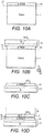
Figure 9 , - Figures 10A to 10D
- illustrate a method of forming an example of the invention involving the transfer of a SiGe layer between substrates,
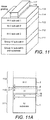
- Figure 11
- is a further example of a device using the invention,
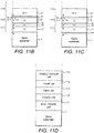
- Figures 11A to 11D
- show examples of the use of the invention, and
- Figure 12
- is an example of a tunnel diode using the invention,
- Figure 13
- is a graph showing the bandgap and lattice parameter of the alloy SiGeSn, showing that it can be lattice matched to GaAs and Ge and the resultant bandgaps.
- A first example of a photovoltaic device in accordance with the invention is illustrated by
Figure 2 . This shows a cross-section of the layers of the lower cell with, if present,further semiconductor layers 5 forming one or more further p-n junctions being indicated by dashed lines. Generally, the structure is similar to that shown inFigure 1 . A p-type GroupIV semiconductor substrate 1, for example germanium, is provided, together with alayer 3 of n-type III-V semiconductor grown on it, the two again meeting atinterface 8. Also again Group V atoms from the III-V layer 3 diffuse into the Group IV layer forming an n-type region 4 adjacent to theinterface 8, which provides ap-n junction 2 where that region meets the remaining p-type part of the Group IV material. However, a thin layer ofsilicon 6 is first provided between thelayer 3 and theGroup IV substrate 1. (Possibilities for the particular Group IV semiconductor material are discussed later below, but the material is not silicon itself. Possibilities for the Group III-V material are also discussed later.) -
Figure 3 shows a second example, which is similar to the first except alayer 7 of epitaxial Group IV semiconductor (other than silicon itself) is first grown on theSi layer 6 before thenucleation layer 3 of III-V material is grown on that. In general, thislayer 7 could be doped initially, as it is grown, either p- or n-type. - In both these examples, the
silicon layer 6 acts to control the diffusion of the Group V atoms from thelayer 3 into the Group IV material. The silicon acts as a barrier to the Group V diffusion and so under the same set of processing conditions used to form the device thep-n junction 2 is shallower, i.e. the position of the p-n junction is closer to theinterface 8 between the Group IV semiconductor and the nucleation layer. The barrier is not total; it reduces, rather than eliminates entirely, the Group V diffusion into the Group IV material that is on the opposite side of the Si barrier from the III-V material that is the source of the Group V atoms. Setting the barrier thickness can be used to control the depth of thep-n junction 2. - In both those examples, the preferred thickness of the
barrier 6 is 3 mono layers (7.5 Å) of silicon or less. Indeed, it may be less than a single complete mono layer. The 3 mono layers is the preferred maximum thickness for the silicon layer because the silicon layer is strained (because it is trying to match the lattice parameter of the Group IV semiconductor). Above that critical thickness, dislocations form in the silicon to relieve the strain, and those dislocations would be disadvantageous to device performance. The range up to 3 monolayers also produces the depths of junction preferred in photovoltaic devices. - In the second example (
Figure 3 ) the thickness of theGroup IV epilayer 7 should preferably not exceed the distance over which the Group V atoms diffuse through the material of that Group IV semiconductor material during the processing of the device, since beyond that distance the amount of Group V atoms traversing the Si barrier will be minimal. Typically, that distance is up to a 1µm, depending on the Group V species being used and the temperatures of the steps of the processing of the device. - (A point to note about the example of
Figure 3 is while generally thep-n junction 2 is on the other side ofsilicon barrier 6 from the III-V layer, the invention generally includes the case where thebarrier 6 limits the diffusion of the Group V atoms but not enough pass through the barrier to convert the Group IV material to n-type, the p-n junction being at, or around*, the barrier (*a p-n junction of course having an extent larger than the few mono layers of the barrier).) -
Figures 4 and5 show third and fourth examples having the same layers respectively as the first and second examples (Figures 2 and3 ), but anepitaxial layer 10 of p-type Group IV semiconductor is first provided before thesilicon layer 6 and the III-V layer 3 are grown. In this particular example the epi-layer 10 is grown on thesubstrate 1, but having intermediate layers is possible. Having thelayer 10 as an epi-layer also helps to accurately control the thickness and doping profile of the junction in the Group IV semiconductor material. Preferablylayer 10 is thick enough that thep-n junction 2 forms in thisGroup IV epilayer 10, as shown, rather than in the substrate 1 (or in an intermediate layer of Group IV material), but the latter are not excluded. Note also however that thatsubstrate 1 need not be Group IV material since the Group IV epi-layer 10 can be grown on other materials. -
Figures 6 and7 show fifth and sixth examples having the same layers respectively as the first and third examples (Figures 2 and4 ), but anepitaxial layer 9 of n-type III-V semiconductor material is first provided on the Group IV layer(s) before thesilicon layer 6 and the main III-V layer 3 are grown. Again, the silicon layer acts as a barrier to control the diffusion of Group V atoms from thelayer 3 into the Group IV material on the other side of thebarrier 6. The Group IV material is also doped by Group V atoms diffusing fromlayer 9. For the presence of the Si barrier to make a significant difference to the level of doping in the Group IV layer from the group III-V layer on the other side of the barrier this III-V epilayer 9 should be thinner than the distance the Group V atoms from thelayer 3 will diffuse throughlayer 9 under the processing conditions of the device. - An example of the Group IV semiconductor material used to be the material in which the p-n junction is formed is germanium. Also germanium substrates are readily available. The preferred orientations for germanium as the substrate are slightly misaligned from (100) and (111). (Substrates misaligned from exact crystal planes are known generally in the art.)
- Group IV semiconductors other than germanium can also be used, such as silicon-germanium and silicon-germanium-tin. SiGe, and SiGeSn, are not available as a basic substrate but can be grown lattice matched on GaAs. Such SiGe or SiGeSn can also be removed from its original GaAs substrate and attached to a cheaper substrate before use in the invention. Examples of this process are described later below. SixGe1-x with a composition with x of up to at least 0.04, and perhaps x = 0.06 or more, may be used, but preferably x is in the range 0.01 <= x <= 0.03. The corresponding lattice mismatch of the SixGe1-x with GaAs will be about 0.04% for every change of 0.01 in x away from the lattice matched condition at about x = 0.018.
Figure 13 is a graph showing the bandgap and lattice parameter of the alloy SiGeSn, showing that it can be lattice matched to GaAs with a bandgap range for the SiGeSn of 0.66-1.1eV. It also shows that SiGeSn can be lattice matched to Ge and since the lattice parameter of Ge is fairly close to that of GaAs the range of bandgaps over which SiGeSn can be lattice matched to Ge is similar to that given above for SiGeSn lattice matched to GaAs. SiGeSn is lattice matched to GaAs where the ratio of Si to Sn is approximately 4:1. Where for example the proportion of Si is 2% and that of Sn is 0.5% this provides a larger bandgap than SiGe lattice matched to GaAs, where the proportion of Si is 8% and that of Sn is 2% the bandgap is wider, and where the proportions are much larger the bandgap can extend further - for example at the limit of 80% Si and 20% Sn the bandgap of that material is around 1.1eV. - As is known in the art, the
nucleation layer 3 can be made from various III-V materials, such as InGaAs, InGaP. Other materials are InGaAsP, AlGaAs, AlGaAsP, GaAs, GaAsP, AlAs, InGaP, InGaAs, AlInGaAs, AlInGaP, etc.. They also include those including Sb (or possibly Bi) as the, or a one of, the Group V atom(s) of the material. As is known in the art most of these materials can be grown lattice matched, or nearly so, to at least one of germanium, silicon, or silicon-germanium, silicon-germanium-tin. - Many of these materials contain As and/or P for the Group V atoms. It is noted here that both As and P diffuse from the Group III-V material into the Group IV material, with, for Ge at least for the Group IV material, As diffusing further and faster than P.
- Where there is more than one III-V epitaxial layer (e.g. the examples of
Figures 6 and7 haveepitaxial layers 3 and 9) it is preferred that these layers of have the same composition in terms both the Group III and V atoms making up the basic material but also in doping provided during deposition. However differences are possible and that may be useful to control the doping profile in the Group IV region. Indeed differences within a layer are also not excluded. - Similarly where there is more than one Group IV epitaxial layer (e.g. the example of 5) it is preferred that these layers have the same composition in terms of both the Group IV atoms making up the basic material but also in doping provided before the Group V diffusion discussed above, e.g. during deposition of the Group IV material. However differences are possible. Indeed differences in composition and/or doping within a layer are also not excluded.
- However, as is frequently done in the art for epitaxial layers, even when the epi-layer and the substrate are the same basic material, it is preferred for group IV epilayer and the substrate (
Figures 4 ,5 and7 ) to have different doping. - As foreshadowed above with the examples of SiGe and SiGeSn grown on GaAs, materials for the
Group IV layer 10 can be grown on substrates of non-Group IV materials. - Some doping concentrations that may be used, or a are preferred, are as follows. For the III-V layer at the interface with the Group IV layer the doping concentration would normally be greater than 1 x 10¹⁷ atoms per cm3; more preferably it would be greater than 1 x 10¹⁸ atoms per cm3, and still more preferably it would be between 1 x 10¹⁸ atoms per cm3 and 5 x 10¹⁸ atoms per cm3. The number of diffused Group V atoms forming the doping in the Group IV material would normally be greater than 1 x 10¹⁷ atoms per cm3; it would preferably be greater than 1 x 10¹⁸ atoms per cm3 and may be greater than 6 x 10¹⁸ atoms per cm3. For the remainder of the Group IV layer (not diffused significantly by the Group V atoms) the doping concentration would normally be less than 4 x 10¹⁸ atoms per cm3; preferably it would be between 5 x 10¹⁶ atoms per cm3 and 2 x 10¹⁸ atoms per cm3 and more preferably it would be between 1 x 10¹⁷ atoms per cm3 and 1 x 10¹⁸ atoms per cm3.
- The
silicon layer 6 and other layers can be grown using conventional techniques. Some possible methods are as follows. - The silicon layer can, for example, be grown in a conventional MOCVD reactor that is also used to provide the epitaxy of the III-V layers (such a tool is conventionally used for III-V epitaxy of multi-junction photovoltaic devices). This is particularly suited to, but not limited to, the first example (
Figure 2 ) since the germanium substrate (taking that as an example of the Group IV semiconductor material) can be placed straight in the MOCVD reactor, which is then used to grow both the silicon and III-V layers in turn. Silicon is used as a dopant source in such reactors and is therefore available to be used to deposit the silicon directly onto the germanium substrate prior to III-V nucleation layer. - The
silicon layer 6 can also be grown epitaxially in a CVD deposition tool used for the growth of germanium, silicon and silicon-germanium or silicon-germanium-tin. This particularly suited to, but is not limited to, the second example (Figure 3 ) since the germanium etc. substrate can first be placed in the tool and then the silicon and Ge epitaxial layers 6 and 7 grown in turn. The work piece can then be transferred to a MOCVD rector (preferably using a cluster tool arrangement so thatgermanium epitaxial layer 7 remains clean) for deposition of the III-V layer 3. - MBE may also be used for the deposition of III-V materials or of silicon.
-
Figure 8 is a plot from a secondary ion mass spectrometer comparing samples of multi-junction tandem cell device having a InGaAs/Ge junction for the bottom cell (a) with and (b) without the silicon layer of the invention directly at the interface. The vertical axis is the concentration of As atoms in the Ge in atoms / cm3 and the horizontal axis is the depth into the Ge layer in microns. The graph clearly shows that with the silicon layer the As dopant diffused into the InGaAs layer is confined to a depth of 1 µm into the Ge layer ((a)), while in the control without a Si layer, but otherwise with same process conditions, the As atoms have penetrated to about 4 µm((b)). Further the concentration of As atoms is lower in the sample with the Si layer. These observations demonstrate that the Si layer acts as a barrier to diffusion of the As. Similar results are obtained with III-V semiconductor materials having different Group V atoms. - Triple junction photovoltaic structure samples having a silicon layer in accordance with the invention have also been measured to provide a useful increase in the maximum power output when irradiated by 1-sun compared to those without, and also in the open circuit voltage (Voc).
-
Figure 9 shows another example of a multi-junction solar cell, which makes use of the invention, this time illustrating all the cells. The Figure shows the tandem arrangement of the cells of the device (each of which is made up of various semiconductor layers, but these are not shown in detail). This device starts with aGaAs substrate 91 on which is grown aSiGe cell 92 in accordance with the invention (so comprising a SiGe layer having the p-n junction, a Si diffusion barrier layer and a III-V layer above (for example GaInP) that providing the doping, none of which are shown in detail in the Figure within the cell 92). Above that are provided aGaAs cell 94 and aInGaP cell 96.Tunnel diodes window layer 97 protects the device but allows the light in andmetal contact lines 99 thereon collect the current produced by the device. Finally ananti-reflective coating 98 covers the window. -
Figure 9A shows an example of thebottom cell 92 andsubstrate 91 ofFigure 9 in more detail (although of course use of this example is not limited to the particular example ofFigure 9 ). This has the structure of the example ofFigure 4 with thesubstrate 1 being GaAs. On that is grown an epi-layer 10 of p-type SiGe largely (or exactly) lattice matched to the GaAs. On that is grown theSi diffusion 6 barrier and on that a III-V nucleation layer 3, again largely (or exactly) lattice matched to the SiGe. The Group V atoms diffuse fromlayer 3, under the conditions of the deposition oflayer 3 and of subsequent processing steps, controlled by thebarrier 6, into the SiGe, doping it to form n-type region 4 next to theinterface 8 and hence thep-n junction 2 in theSiGe layer 10. In a similar example to this theSiGe layer 10 is made instead from SiGeSn.
In this device doping of the SiGe (or SiGeSn) with Group V atoms from theGaAs substrate 1 is a potential problem: overdoping of the SiGe from p-type to n-type by As atoms to form another p-n junction in the SiGe near the interface between theSiGe 10 and thesubstrate 1.
This can be addressed in two ways. First, anotherSi barrier 14 can be provided at that interface to reduce the diffusion to a level where the SiGe remains p-type. (A thickness of 7.5Å, or 3 atomic layers, is for theSi barrier
Another way is to avoid the problem by transferring the SiGe onto a different substrate before subsequent processing steps are carried out. This transfer is described below and in our International patent application published asWO2010094919 published on 26 August 2010 . - For this the
SiGe layer 10 can be grown (Figure 10A ) on theGaAs substrate 1 using an epitaxy process, lattice matched, using a gas mixture of a germanium containing precursor (e.g. GeH4, GeCl4, etc) and a silicon containing precursor (e.g. SiH4, SiH2Cl2, SiHCl3, disilane, etc) with a carrier gas (e.g. H2). The SiGe layers 10 can be in-situ doped with p-type dopants, using gaseous or solid doping sources including, but not limited to, diborane. Thelayer 10 can be grown, for example, at atmospheric pressure or reduced pressure in therange 1∼1000 Torr, and temperature 350°C∼800°C. A range of GaAs substrates may be used including p- type, n-type and semi-insulating, and the wafers may be cleaned ex-situ or in the process chamber prior to epitaxy. Crystallinity properties of theSiGe layer 10 may be measured using X-ray diffraction techniques, for example to check lattice matching, and the thicknesses of the layers may typically be monitored using variable angle spectroscopic ellipsometry, although other techniques are available. - In this process, the change of material composition between the GaAs substrate and the
SiGe layer 10 provides a hetero-interface which acts as a good etch-stop, enabling the GaAs substrate to be removed conveniently and accurately to leave a smooth surface of theSiGe layer 10. Some of the GaAs substrate may be removed by mechanical means if this provides more rapid or otherwise convenient or cost-effective manufacture process. For example, if the GaAs substrate is 500 µm thick, about 400 µm may be removed by grinding from which the GaAs material can be more easily recovered and reused, and the final 100 µm may be removed by selective wet etching. - The photovoltaic cell structure resulting from use of this method can be of lighter weight because the substrate thickness has been removed, which may be important particularly in space-based applications. An alternative base which has favourable flexibility, thermal behaviour, or other desirable mechanical or electrical properties may be advantageously provided. Replacement of the substrate with a heatsink can result in more efficient thermal conduction away from the device because the substrate no longer acts to reduce the flow of heat. The heatsink or another metallic base layer can act directly as a conductive electrode to the bottom of the device.
- A particular technique is illustrated in
Figures 10A - 10D . Starting with aGaAs substrate 1, alayer 10 of SiGe is grown epitaxially as previously described, and as shown inFigure 10A . A layer transfer technique is then used to remove all but a thin layer of the GaAs substrate. The layer transfer may be achieved using a proprietary exfoliation technique such as Smart Cut (RTM) or similar, in which acleave plane 12 is formed in the GaAs substrate just beneath thelayer 10 of SiGe. Thecleave plane 12 may be formed using ion beam implant techniques to deposit hydrogen or helium atoms at a precise depth determined by the beam particle energy, for example at depths of up to about 1.5 µm, making the technique practical in the present context if the thickness of the layer of SiGe is of approximately this thickness. - An
alternative base 13 is then bonded to theSiGe layer 10. As shown inFigure 10B the alternative base may be an oxidised silicon wafer such that the SiGe layer is bonded to a layer of SiO2, although other bases may be used such as the metallic heat sink layer discussed above. Some other bases which can be used are metallic, glass and semiconductor bases, which may themselves already comprise two or more layers selected from metal, semiconductor and insulator materials, and may include active elements such as one or more photovoltaic junctions. The bulk of the GaAs substrate is then separated from the structure, and the fine remaining layer of GaAs is removed, for example by selective wet etching, to leave thelayer 10 of SiGe on an alternative base such as the oxidised silicon wafer discussed, and as shown inFigure 10C . Subsequent layers of the device are then formed as shown inFigure 10D , for example theSi barrier 6 and the III-V layer 3 andsubsequent layers 5. - One variation of the described technique is to form the cleave plane just above the interface with the substrate, within the lower SiGe layer. Following layer transfer the transferred SiGe is already exposed for any necessary further preparation. The residual SiGe remaining on the GaAs substrate can be removed, at least partially using a wet etch selective for SiGe and ineffective on GaAs, to leave a reuseable GaAs substrate wafer.
- A wide variety of different alternative bases may be contemplated for the structure of
Figure 10D , including metallic, glass, and semiconductor bases, which may themselves already comprise two or more layers selected from metal, semiconductor, and insulator materials, and may include active elements such as one or more photovoltaic junctions. The initial formation of the SiGe layer on a GaAs substrate provides an ideal etchstop for accurate removal of the remaining GaAs following cleaving or exfoliation. -
Figure 11 shows a further example of a multi-junction solar cell, which makes use of the invention. This shows a five cell solar cell device, again with all the cells connected in tandem. These are, in order from the substrate, aGe cell 111, anotherGe cell 112, aGaInAs cell 113, anAlGaInAs cell 114 and a AlGaInP cell 115 (covered by a heavily n-type contact layer 116 and metal lines 117). In this device the invention is used to form theGe cell 112; this has an interface with the III-V material of thecell 113 above, which provides the Group V dopant so theSi diffusion barrier 6 is provided at the interface betweencells -
Figure 11A shows an example of thebottom cells Figure 11 in more detail, although of course its use is not limited to the particular example ofFigure 11 . - The
lowest cell 111 has a p-type Group IV substrate 1 (for example Ge) on which is grown n-type Group IV (for example Ge) epilayer to form the first p-n junction. In order to provide a low resistance contact to thenext cell 112 thelayers 16 of a tunnel diode are deposited next. On top of that are formed epilayer 10 of p-type Group IV material (for example Ge) followed by asilicon diffusion barrier 6 and a Group III-V epilayer 3 to form in the manner of the examples above ap-n junction 2 between the n-type material 4 of theepilayer 10 doped by Group V atoms diffused through thebarrier 6 from theepilayer 3 and the remainder of theGroup IV layer 10, thereby formingcell 112. -
Figure 11B shows another example that is similar to that ofFigure 11A . However in this example first cell does not include the substrate but is made of an additional Group IV epi-layer 17 that is p-type grown on the substrate 1 (generally lattice matched to the substrate) with the n-typeGroup IV layer 15 grown on top of that to form the p-n junction of the first cell. - In a particular example of the example of
Figure 11B the material of the substrate is GaAs (as marked inFigure 11B (and inFigure 11C )). The Group IV layers are then preferably ones that can be grown generally lattice matched to that, examples of which are SiGe and SiGeSn. SiGe provides a bandgap of 0.66eV when lattice matched to GaAs and SiGeSn provides a bandgap of greater than that, up to ∼1.1eV. If two bandgaps of greater than 0.66eV are desired, while remaining lattice matched to GaAs, then thelowest cell 111 and thenext cell 112 can both be made of SiGeSn but with different compositions to each other to provide the desired bandgaps. -
Figure 11C shows a further example that is similar to that ofFigure 11B but in this example an additionalSi diffusion barrier 14 is provided (like that of example ofFigure 9B ) to prevent the formation of an unwanted p-n junction in the GroupIV material layer 17 when the substrate is a III-V material (for example GaAs). -
Figure 11D shows another example of a multi-junction solar cell. As with the examples ofFigures 11B and IIC a first cell of SiGe or SiGeSn is provided on a GaAs substrate and above that is provided a second cell of SiGeSn. In this example a further three cells are provided, also in tandem: a third cell of GaAs above the second cell, a fourth cell of InGaP above the third cell and a fifth cell of AlGaAs or AlInGaP above the fourth cell. All the cells are all lattice matched to the GaAs substrate. (Although AlGaAs does not have exactly the same lattice parameter as GaAs, it is nearly equal enough so to still be lattice matched, only with a small strain where the AlGaAs layer is below the critical thickness where strain relieving dislocations would occur. This applies throughout its compositional range of the proportion of aluminium to gallium. In this example, the other materials have compositions that are exactly lattice matched to GaAs, which compositions are used for preference.) An example of the bandgaps of the cells are in order from the first cell to the last: 0.7eV, 1.0eV, 1.4eV, 1.8eV 2.0eV. - Each cell therefore absorbs a different part of the spectrum of the light falling on the device. The device may be provided, if desired, with the Si barriers, tunnel diodes, window layers etc. mentioned in the other examples. Also the substrate may be removed as described with reference to
Figure 10A to 10D . Further the materials of the cells may be grown not on GaAs itself but on another substrate that is lattice matched to GaAs. Other layers may be used between the light absorbing cells, for example, tunnel diodes, and these are preferably lattice matched to the cells and also preferably to the substrate. -
Figure 12 shows the layers of an example of another aspect of the invention. Here theSi diffusion barrier 6 between Group IV 10' and Group III-V layers 3' controls the diffusion of Group V atoms through the barrier into Group IV material that is already n-type, the diffused region 4' produced therefore being highly n-doped. In this example, layers 3' and 4' form atunnel diode 16. - The example shown in
Figure 12 shows the tunnel diode in combination with a Group IV photocell (and so this example will be of use in tandem photovoltaic devices). A p-typeGroup IV substrate 1 is provided on which is grown an n-type Group IV epilayer 10', which junction provides the photovoltaic cell. Above that is provided a thinSi diffusion barrier 6 and on top of that a highly doped layer 3' of Group III-V material the Group V atoms of which diffuse through the barrier to form the highly doped n++ region 4'. Above that may be grownother layers 5 for example other photovoltaic cells, for example in III-V materials. The highly doped n++ Group IV region 4' and the highly doped p++ III-V layer 3' form a low resistance tunnel diode. 16, which allows photo current produced by the p-n junction betweenlayers 1 and 10' to be conducted to the layers above without excessive resistive loss. - As with the earlier examples above the silicon barrier need not be exactly at the interface between the Group IV and Group III-V materials but may be at a distance to one side where it can still influence the diffusion of the Group V atoms.
- In the above examples, the subcells may alternatively be grown in reverse order on a GaAs substrate (or a substrate lattice matched to GaAs, or other substrate appropriate to the lattice parameter of the structure) starting with the wider bandgap cells and then followed by in order smaller bandgap cells ending for example with the SiGe / SiGeSn cell. A sacrificial layer is provided between the widest gap cell and the substrate allowing the cells to be removed and transferred to a suitable handle or heat sink, inverted so that the narrowest bandgap cell is next to the substrate and the widest bandgap cell receives the incident light first.
- Devices using these materials, typically solar cells, are usually manufactured by first providing a semiconductor material having the necessary layers, or at least some of those. Usually the material is made uniformly over a whole semiconductor wafer. The material is then processed with lithographic techniques to form individual devices and connections. The manufacture of the material is often carried out by a different manufacturer from that performing the lithographic and packaging steps.
That part of the n-type Group V doped region in the Group IV semiconductor layer that is to a particular side of the silicon layer may be doped by Group V atoms of at least one of the kinds of those forming that part the Group III-V semiconductor that is on the opposite side of the silicon layer.
Claims (14)
- A semiconductor material comprising:a Group IV semiconductor material layer (1,4,7,10), the material not being silicon,a layer of Group III-V semiconductor material (3,9) formed of at least one kind of Group III atoms and at least one kind of Group V atoms, and having an interface (8) with the Group IV semiconductor layer, the group IV semiconductor material layer being lattice matched to the Group III-V semiconductor material layer;a silicon layer (6) either at the interface between the III-V semiconductor layer and the Group IV semiconductor layer, or in either the Group IV semiconductor layer, or the III-V semiconductor layer, spaced from the interface to control the diffusion of the Group V atoms into the Group IV semiconductor layer,an n-type Group V doped region (4) in the Group IV semiconductor layer that has a border with the interface and that is doped by Group V atoms which have diffused from the layer of Group III-V semiconductor material through the silicon layer.
- A semiconductor material as claimed in claim 1 wherein the Group V doped region in the Group IV semiconductor layer provides a p-n junction (2) with a p-type region in the Group IV layer.
- A semiconductor material as claimed in claim 1, wherein the Group V doped region in the Group IV layer and the Group III-V layer form a tunnel diode at the interface.
- A semiconductor material as claimed in any preceding claim wherein the Group IV semiconductor material layer is germanium.
- A semiconductor material as claimed in any one of claims 1 to 3 wherein the Group IV semiconductor material layer is silicon-germanium, or is silicon-germanium-tin.
- A semiconductor material as claimed in any preceding claim wherein the Group III-V material comprises Group III atoms that are one or more of Al, Ga, In and comprises Group V atoms that are one or more of P, As, Sb, Bi.
- A semiconductor material as claimed in any preceding claim wherein the Group IV layer (10) comprises an epitaxial Group IV semiconductor layer (7) between the silicon layer (6) and the III-V semiconductor layer (3).
- A semiconductor material as claimed in any preceding claim wherein the Group IV semiconductor layer comprises a substrate layer (1) and an epitaxial layer (10) grown on the substrate layer.
- A semiconductor material as claimed in any preceding claim wherein the silicon layer (6) has a thickness of less than or equal to 7.5 Å.
- A semiconductor material as claimed in any preceding claim comprising a second layer of Group III-V semiconductor material (1) having an interface with the Group IV semiconductor layer (10) at the opposite side of the Group IV layer to the interface (8) with the first Group III-V layer (3) and comprising a second silicon layer (14) at the interface between the second III-V semiconductor layer and the Group IV layer.
- A photovoltaic device comprising a light absorbing cell comprising a semiconductor material as claimed in any preceding claim.
- A method of making a semiconductor material comprising:providing a Group IV semiconductor material layer (1,4,7,10), the material not being silicon,providing a layer of Group III-V semiconductor material (3,9) formed of at least one kind of Group III atoms and at least one kind of Group V atoms, and having an interface (8) with the Group IV semiconductor layer, the group IV semiconductor material layer being lattice matched to the Group III-V semiconductor material layer,providing a silicon layer (6) either at the interface between the III-V semiconductor layer, or in either the Group IV semiconductor layer or the III-V semiconductor layer, spaced from the interface,diffusing Group V atoms from the Group III-V material layer through the silicon layer to dope the Group IV material to form an n-type Group V doped region in the Group IV semiconductor layer that has a border with the interface.
- A method as claimed in claim 12 wherein the diffusing of the Group V atoms forms a p-n junction (2) in the Group IV layer.
- A method as claimed in claim 12 wherein the diffusing of the Group V atoms is into a region of the Group IV layer that was already n-type to form a region of n-type doping having a higher concentration on n-type dopants.
Applications Claiming Priority (2)
| Application Number | Priority Date | Filing Date | Title |
|---|---|---|---|
| US201161528650P | 2011-08-29 | 2011-08-29 | |
| PCT/GB2012/051982 WO2013030531A1 (en) | 2011-08-29 | 2012-08-14 | Photovoltaic device |
Publications (2)
| Publication Number | Publication Date |
|---|---|
| EP2745330A1 EP2745330A1 (en) | 2014-06-25 |
| EP2745330B1 true EP2745330B1 (en) | 2020-06-03 |
Family
ID=46727255
Family Applications (3)
| Application Number | Title | Priority Date | Filing Date |
|---|---|---|---|
| EP12750800.0A Ceased EP2745328A1 (en) | 2011-08-29 | 2012-08-14 | Photovoltaic device |
| EP12750801.8A Not-in-force EP2745329B1 (en) | 2011-08-29 | 2012-08-14 | Photovoltaic device |
| EP12753571.4A Active EP2745330B1 (en) | 2011-08-29 | 2012-08-14 | Photovoltaic device |
Family Applications Before (2)
| Application Number | Title | Priority Date | Filing Date |
|---|---|---|---|
| EP12750800.0A Ceased EP2745328A1 (en) | 2011-08-29 | 2012-08-14 | Photovoltaic device |
| EP12750801.8A Not-in-force EP2745329B1 (en) | 2011-08-29 | 2012-08-14 | Photovoltaic device |
Country Status (7)
| Country | Link |
|---|---|
| US (4) | US10263129B2 (en) |
| EP (3) | EP2745328A1 (en) |
| JP (3) | JP6228119B2 (en) |
| CN (2) | CN107845690B (en) |
| AU (2) | AU2012300694C1 (en) |
| ES (1) | ES2813938T3 (en) |
| WO (3) | WO2013030530A1 (en) |
Families Citing this family (35)
| Publication number | Priority date | Publication date | Assignee | Title |
|---|---|---|---|---|
| US20170141256A1 (en) * | 2009-10-23 | 2017-05-18 | Alta Devices, Inc. | Multi-junction optoelectronic device with group iv semiconductor as a bottom junction |
| US11646388B2 (en) | 2012-09-14 | 2023-05-09 | The Boeing Company | Group-IV solar cell structure using group-IV or III-V heterostructures |
| US9985160B2 (en) * | 2012-09-14 | 2018-05-29 | The Boeing Company | Group-IV solar cell structure using group-IV or III-V heterostructures |
| US11495705B2 (en) | 2012-09-14 | 2022-11-08 | The Boeing Company | Group-IV solar cell structure using group-IV or III-V heterostructures |
| US9099595B2 (en) | 2012-09-14 | 2015-08-04 | The Boeing Company | Group-IV solar cell structure using group-IV or III-V heterostructures |
| US9997659B2 (en) | 2012-09-14 | 2018-06-12 | The Boeing Company | Group-IV solar cell structure using group-IV or III-V heterostructures |
| US10903383B2 (en) | 2012-09-14 | 2021-01-26 | The Boeing Company | Group-IV solar cell structure using group-IV or III-V heterostructures |
| KR20140095738A (en) * | 2013-01-25 | 2014-08-04 | 삼성전자주식회사 | Transistors and methods of manufacturing the same |
| CN103199130B (en) * | 2013-03-15 | 2016-03-09 | 中国科学院苏州纳米技术与纳米仿生研究所 | Formal dress four-junction solar battery and preparation method thereof |
| CN103199141A (en) * | 2013-03-15 | 2013-07-10 | 中国科学院苏州纳米技术与纳米仿生研究所 | Four-junction cascading solar battery and preparation method thereof |
| CN103137766B (en) * | 2013-03-15 | 2015-09-09 | 中国科学院苏州纳米技术与纳米仿生研究所 | Triple-junction monolithic solar cell and preparation method thereof |
| EP2782145A1 (en) * | 2013-03-21 | 2014-09-24 | Alcatel Lucent | Method for manufacturing a multijunction photovoltaic device and resulting multijunction photovoltaic device |
| CN103151414B (en) * | 2013-04-03 | 2016-04-27 | 中国科学院苏州纳米技术与纳米仿生研究所 | Formal dress triple-junction monolithic solar cell and preparation method thereof |
| CN103219412B (en) * | 2013-04-03 | 2016-03-09 | 中国科学院苏州纳米技术与纳米仿生研究所 | Triple-junction monolithic solar cell and preparation method thereof |
| CN103259193B (en) * | 2013-05-14 | 2016-03-09 | 中国科学院苏州纳米技术与纳米仿生研究所 | A kind of 1300nm ~ 1550nm is containing the preparation method of the semiconductor laser of bismuthide |
| CN103311353B (en) * | 2013-05-29 | 2016-09-07 | 中国科学院苏州纳米技术与纳米仿生研究所 | three-junction cascade solar cell and preparation method thereof |
| GB2515322A (en) * | 2013-06-19 | 2014-12-24 | Univ Surrey | Light Receiving Device |
| US20140373906A1 (en) * | 2013-06-25 | 2014-12-25 | Solar Junction Corporation | Anti-reflection coatings for multijunction solar cells |
| CN103426965B (en) * | 2013-08-16 | 2016-12-28 | 中国科学院苏州纳米技术与纳米仿生研究所 | Solaode and preparation method thereof |
| CN104638060B (en) * | 2013-11-13 | 2018-03-06 | 中国电子科技集团公司第十八研究所 | The preparation method of hetero-junctions thermophotovoltaic |
| CN104638046B (en) * | 2013-11-13 | 2017-05-03 | 中国电子科技集团公司第十八研究所 | Heterojunction thermophotovoltaic cell with Ge (germanium) substrate |
| CN103839774A (en) * | 2014-02-25 | 2014-06-04 | 清华大学 | SiGeSn layer and forming method thereof |
| US9548408B2 (en) * | 2014-04-15 | 2017-01-17 | L-3 Communications Cincinnati Electronics Corporation | Tunneling barrier infrared detector devices |
| JP2016082041A (en) * | 2014-10-15 | 2016-05-16 | 株式会社リコー | Compound semiconductor solar cell and method of manufacturing compound semiconductor solar cell |
| KR20180107174A (en) * | 2016-01-29 | 2018-10-01 | 알타 디바이씨즈, 인크. | Multi-junction optoelectronic devices with IV junction semiconductors in bottom junction |
| CN105720126B (en) * | 2016-04-27 | 2017-07-28 | 天津三安光电有限公司 | A flip-chip four-junction solar cell structure and preparation method thereof |
| US20170365732A1 (en) | 2016-06-15 | 2017-12-21 | Solar Junction Corporation | Dilute nitride bismide semiconductor alloys |
| CN106531836A (en) * | 2016-11-25 | 2017-03-22 | 罗雷 | Four-junction solar energy cell |
| US10593818B2 (en) * | 2016-12-09 | 2020-03-17 | The Boeing Company | Multijunction solar cell having patterned emitter and method of making the solar cell |
| CN108807284B (en) * | 2017-04-28 | 2020-06-26 | 环球晶圆股份有限公司 | A kind of epitaxial bonding substrate and its manufacturing method |
| US11342498B2 (en) * | 2018-01-08 | 2022-05-24 | Integrated Silicon Solution (cayman) Inc. | High density 3D magnetic random access memory (MRAM) cell integration using wafer cut and transfer |
| CN111477677B (en) * | 2020-05-27 | 2024-12-06 | 北京时代全芯存储技术股份有限公司 | Diode structure and method for manufacturing the same |
| CN113066907B (en) * | 2021-06-03 | 2021-08-27 | 南昌凯迅光电有限公司 | Preparation method of three-junction gallium arsenide solar cell with nano-mesh surface electrode |
| EP4459682A1 (en) | 2023-05-03 | 2024-11-06 | Valstybinis moksliniu tyrimu institutas Fiziniu ir technologijos mokslu centras | Method for making multijunction photovoltaic device comprising a gaasbi subcell |
| CN118658918B (en) * | 2024-07-19 | 2025-11-04 | 江苏仲磊芯半导体有限公司 | A four-junction solar cell and its fabrication method |
Family Cites Families (32)
| Publication number | Priority date | Publication date | Assignee | Title |
|---|---|---|---|---|
| JPS63503103A (en) * | 1985-09-30 | 1988-11-10 | 鐘淵化学工業株式会社 | Multi-junction semiconductor device |
| JPS6437060A (en) * | 1987-08-03 | 1989-02-07 | Nippon Telegraph & Telephone | Semiconductor element |
| US6281426B1 (en) * | 1997-10-01 | 2001-08-28 | Midwest Research Institute | Multi-junction, monolithic solar cell using low-band-gap materials lattice matched to GaAs or Ge |
| US5944913A (en) * | 1997-11-26 | 1999-08-31 | Sandia Corporation | High-efficiency solar cell and method for fabrication |
| US6380601B1 (en) * | 1999-03-29 | 2002-04-30 | Hughes Electronics Corporation | Multilayer semiconductor structure with phosphide-passivated germanium substrate |
| JP3657143B2 (en) * | 1999-04-27 | 2005-06-08 | シャープ株式会社 | Solar cell and manufacturing method thereof |
| US6252287B1 (en) * | 1999-05-19 | 2001-06-26 | Sandia Corporation | InGaAsN/GaAs heterojunction for multi-junction solar cells |
| US6340788B1 (en) * | 1999-12-02 | 2002-01-22 | Hughes Electronics Corporation | Multijunction photovoltaic cells and panels using a silicon or silicon-germanium active substrate cell for space and terrestrial applications |
| US7339109B2 (en) | 2000-06-20 | 2008-03-04 | Emcore Corporation | Apparatus and method for optimizing the efficiency of germanium junctions in multi-junction solar cells |
| JP2002222989A (en) * | 2001-01-26 | 2002-08-09 | Toshiba Corp | Semiconductor light emitting device |
| US6815736B2 (en) | 2001-02-09 | 2004-11-09 | Midwest Research Institute | Isoelectronic co-doping |
| US20030015728A1 (en) * | 2001-07-17 | 2003-01-23 | Motorola, Inc. | Photonic biasing and integrated solar charging networks for integrated circuits |
| US20060162768A1 (en) * | 2002-05-21 | 2006-07-27 | Wanlass Mark W | Low bandgap, monolithic, multi-bandgap, optoelectronic devices |
| US7126052B2 (en) * | 2002-10-02 | 2006-10-24 | The Boeing Company | Isoelectronic surfactant induced sublattice disordering in optoelectronic devices |
| JP5248782B2 (en) * | 2004-01-20 | 2013-07-31 | シリアム・テクノロジーズ・インコーポレーテッド | Solar cell with epitaxially grown quantum dot material |
| US10069026B2 (en) | 2005-12-19 | 2018-09-04 | The Boeing Company | Reduced band gap absorber for solar cells |
| US7872252B2 (en) * | 2006-08-11 | 2011-01-18 | Cyrium Technologies Incorporated | Method of fabricating semiconductor devices on a group IV substrate with controlled interface properties and diffusion tails |
| US20080257405A1 (en) * | 2007-04-18 | 2008-10-23 | Emcore Corp. | Multijunction solar cell with strained-balanced quantum well middle cell |
| US20090014061A1 (en) | 2007-07-10 | 2009-01-15 | The Board Of Trustees Of The Leland Stanford Junior University | GaInNAsSb solar cells grown by molecular beam epitaxy |
| US8202788B2 (en) | 2008-06-26 | 2012-06-19 | Nanyang Technological University | Method for fabricating GaNAsSb semiconductor |
| CN101431117A (en) * | 2008-11-24 | 2009-05-13 | 北京索拉安吉清洁能源科技有限公司 | Multi-junction solar cell with doping blocking layer |
| US20100147366A1 (en) * | 2008-12-17 | 2010-06-17 | Emcore Solar Power, Inc. | Inverted Metamorphic Multijunction Solar Cells with Distributed Bragg Reflector |
| GB2467935B (en) | 2009-02-19 | 2013-10-30 | Iqe Silicon Compounds Ltd | Formation of thin layers of GaAs and germanium materials |
| GB2467934B (en) * | 2009-02-19 | 2013-10-30 | Iqe Silicon Compounds Ltd | Photovoltaic cell |
| WO2010102345A1 (en) * | 2009-03-12 | 2010-09-16 | Shaun Joseph Cunningham | Improved photo-voltaic device and system |
| US20100282305A1 (en) * | 2009-05-08 | 2010-11-11 | Emcore Solar Power, Inc. | Inverted Multijunction Solar Cells with Group IV/III-V Hybrid Alloys |
| US20100282307A1 (en) * | 2009-05-08 | 2010-11-11 | Emcore Solar Power, Inc. | Multijunction Solar Cells with Group IV/III-V Hybrid Alloys for Terrestrial Applications |
| US20100282306A1 (en) * | 2009-05-08 | 2010-11-11 | Emcore Solar Power, Inc. | Multijunction Solar Cells with Group IV/III-V Hybrid Alloys |
| TW201114043A (en) | 2009-10-02 | 2011-04-16 | Epistar Corp | A high efficiency solar cell |
| US20110232730A1 (en) | 2010-03-29 | 2011-09-29 | Solar Junction Corp. | Lattice matchable alloy for solar cells |
| US9214580B2 (en) | 2010-10-28 | 2015-12-15 | Solar Junction Corporation | Multi-junction solar cell with dilute nitride sub-cell having graded doping |
| WO2013074530A2 (en) * | 2011-11-15 | 2013-05-23 | Solar Junction Corporation | High efficiency multijunction solar cells |
-
2012
- 2012-08-14 WO PCT/GB2012/051981 patent/WO2013030530A1/en not_active Ceased
- 2012-08-14 CN CN201711071248.7A patent/CN107845690B/en not_active Expired - Fee Related
- 2012-08-14 ES ES12753571T patent/ES2813938T3/en active Active
- 2012-08-14 US US14/342,061 patent/US10263129B2/en active Active
- 2012-08-14 JP JP2014527730A patent/JP6228119B2/en not_active Expired - Fee Related
- 2012-08-14 US US14/342,016 patent/US20140345679A1/en not_active Abandoned
- 2012-08-14 AU AU2012300694A patent/AU2012300694C1/en not_active Ceased
- 2012-08-14 CN CN201280049676.9A patent/CN103875079B/en not_active Expired - Fee Related
- 2012-08-14 EP EP12750800.0A patent/EP2745328A1/en not_active Ceased
- 2012-08-14 WO PCT/GB2012/051980 patent/WO2013030529A1/en not_active Ceased
- 2012-08-14 EP EP12750801.8A patent/EP2745329B1/en not_active Not-in-force
- 2012-08-14 EP EP12753571.4A patent/EP2745330B1/en active Active
- 2012-08-14 WO PCT/GB2012/051982 patent/WO2013030531A1/en not_active Ceased
- 2012-08-14 US US14/241,987 patent/US20150041863A1/en not_active Abandoned
-
2016
- 2016-01-19 AU AU2016200282A patent/AU2016200282B2/en not_active Ceased
- 2016-12-16 US US15/382,181 patent/US10367107B2/en active Active
-
2017
- 2017-10-12 JP JP2017198245A patent/JP2018026580A/en active Pending
-
2019
- 2019-07-26 JP JP2019137470A patent/JP2019216249A/en active Pending
Non-Patent Citations (1)
| Title |
|---|
| None * |
Also Published As
| Publication number | Publication date |
|---|---|
| US20150041863A1 (en) | 2015-02-12 |
| EP2745329B1 (en) | 2018-09-19 |
| WO2013030529A1 (en) | 2013-03-07 |
| WO2013030530A1 (en) | 2013-03-07 |
| EP2745330A1 (en) | 2014-06-25 |
| JP2014527725A (en) | 2014-10-16 |
| AU2012300694B2 (en) | 2015-10-22 |
| ES2813938T3 (en) | 2021-03-25 |
| AU2016200282B2 (en) | 2017-08-31 |
| AU2016200282A1 (en) | 2016-02-11 |
| EP2745328A1 (en) | 2014-06-25 |
| JP2019216249A (en) | 2019-12-19 |
| CN107845690B (en) | 2020-09-08 |
| US20140326301A1 (en) | 2014-11-06 |
| JP6228119B2 (en) | 2017-11-08 |
| CN103875079B (en) | 2017-12-12 |
| AU2012300694A1 (en) | 2014-03-20 |
| CN103875079A (en) | 2014-06-18 |
| AU2012300694C1 (en) | 2016-04-21 |
| AU2012300694A8 (en) | 2014-04-03 |
| US20170117429A1 (en) | 2017-04-27 |
| WO2013030531A1 (en) | 2013-03-07 |
| JP2018026580A (en) | 2018-02-15 |
| CN107845690A (en) | 2018-03-27 |
| EP2745329A1 (en) | 2014-06-25 |
| US20140345679A1 (en) | 2014-11-27 |
| US10367107B2 (en) | 2019-07-30 |
| US10263129B2 (en) | 2019-04-16 |
Similar Documents
| Publication | Publication Date | Title |
|---|---|---|
| US10367107B2 (en) | Multijunction photovoltaic device having an Si barrier between cells | |
| EP2399300B1 (en) | Method for forming a photovoltaic cell | |
| US10680126B2 (en) | Photovoltaics on silicon | |
| US8344242B2 (en) | Multi-junction solar cells | |
| US9716201B2 (en) | Silicon heterojunction photovoltaic device with wide band gap emitter | |
| US20090288703A1 (en) | Wide Band Gap Window Layers In Inverted Metamorphic Multijunction Solar Cells | |
| US20140196774A1 (en) | Multi-junction iii-v solar cell | |
| GB2501432A (en) | Germanium Based Photovoltaic Cell With GaAs Substrate Removed | |
| US20170365732A1 (en) | Dilute nitride bismide semiconductor alloys |
Legal Events
| Date | Code | Title | Description |
|---|---|---|---|
| PUAI | Public reference made under article 153(3) epc to a published international application that has entered the european phase |
Free format text: ORIGINAL CODE: 0009012 |
|
| 17P | Request for examination filed |
Effective date: 20140321 |
|
| AK | Designated contracting states |
Kind code of ref document: A1 Designated state(s): AL AT BE BG CH CY CZ DE DK EE ES FI FR GB GR HR HU IE IS IT LI LT LU LV MC MK MT NL NO PL PT RO RS SE SI SK SM TR |
|
| DAX | Request for extension of the european patent (deleted) | ||
| STAA | Information on the status of an ep patent application or granted ep patent |
Free format text: STATUS: EXAMINATION IS IN PROGRESS |
|
| 17Q | First examination report despatched |
Effective date: 20170919 |
|
| GRAP | Despatch of communication of intention to grant a patent |
Free format text: ORIGINAL CODE: EPIDOSNIGR1 |
|
| STAA | Information on the status of an ep patent application or granted ep patent |
Free format text: STATUS: GRANT OF PATENT IS INTENDED |
|
| INTG | Intention to grant announced |
Effective date: 20191213 |
|
| GRAS | Grant fee paid |
Free format text: ORIGINAL CODE: EPIDOSNIGR3 |
|
| GRAA | (expected) grant |
Free format text: ORIGINAL CODE: 0009210 |
|
| STAA | Information on the status of an ep patent application or granted ep patent |
Free format text: STATUS: THE PATENT HAS BEEN GRANTED |
|
| AK | Designated contracting states |
Kind code of ref document: B1 Designated state(s): AL AT BE BG CH CY CZ DE DK EE ES FI FR GB GR HR HU IE IS IT LI LT LU LV MC MK MT NL NO PL PT RO RS SE SI SK SM TR |
|
| REG | Reference to a national code |
Ref country code: GB Ref legal event code: FG4D |
|
| REG | Reference to a national code |
Ref country code: AT Ref legal event code: REF Ref document number: 1277931 Country of ref document: AT Kind code of ref document: T Effective date: 20200615 Ref country code: CH Ref legal event code: EP |
|
| REG | Reference to a national code |
Ref country code: DE Ref legal event code: R096 Ref document number: 602012070475 Country of ref document: DE |
|
| REG | Reference to a national code |
Ref country code: NL Ref legal event code: FP |
|
| REG | Reference to a national code |
Ref country code: FI Ref legal event code: FGE |
|
| REG | Reference to a national code |
Ref country code: LT Ref legal event code: MG4D |
|
| PG25 | Lapsed in a contracting state [announced via postgrant information from national office to epo] |
Ref country code: GR Free format text: LAPSE BECAUSE OF FAILURE TO SUBMIT A TRANSLATION OF THE DESCRIPTION OR TO PAY THE FEE WITHIN THE PRESCRIBED TIME-LIMIT Effective date: 20200904 Ref country code: NO Free format text: LAPSE BECAUSE OF FAILURE TO SUBMIT A TRANSLATION OF THE DESCRIPTION OR TO PAY THE FEE WITHIN THE PRESCRIBED TIME-LIMIT Effective date: 20200903 Ref country code: SE Free format text: LAPSE BECAUSE OF FAILURE TO SUBMIT A TRANSLATION OF THE DESCRIPTION OR TO PAY THE FEE WITHIN THE PRESCRIBED TIME-LIMIT Effective date: 20200603 Ref country code: LT Free format text: LAPSE BECAUSE OF FAILURE TO SUBMIT A TRANSLATION OF THE DESCRIPTION OR TO PAY THE FEE WITHIN THE PRESCRIBED TIME-LIMIT Effective date: 20200603 |
|
| PG25 | Lapsed in a contracting state [announced via postgrant information from national office to epo] |
Ref country code: RS Free format text: LAPSE BECAUSE OF FAILURE TO SUBMIT A TRANSLATION OF THE DESCRIPTION OR TO PAY THE FEE WITHIN THE PRESCRIBED TIME-LIMIT Effective date: 20200603 Ref country code: BG Free format text: LAPSE BECAUSE OF FAILURE TO SUBMIT A TRANSLATION OF THE DESCRIPTION OR TO PAY THE FEE WITHIN THE PRESCRIBED TIME-LIMIT Effective date: 20200903 Ref country code: LV Free format text: LAPSE BECAUSE OF FAILURE TO SUBMIT A TRANSLATION OF THE DESCRIPTION OR TO PAY THE FEE WITHIN THE PRESCRIBED TIME-LIMIT Effective date: 20200603 Ref country code: HR Free format text: LAPSE BECAUSE OF FAILURE TO SUBMIT A TRANSLATION OF THE DESCRIPTION OR TO PAY THE FEE WITHIN THE PRESCRIBED TIME-LIMIT Effective date: 20200603 |
|
| REG | Reference to a national code |
Ref country code: AT Ref legal event code: MK05 Ref document number: 1277931 Country of ref document: AT Kind code of ref document: T Effective date: 20200603 |
|
| PG25 | Lapsed in a contracting state [announced via postgrant information from national office to epo] |
Ref country code: AL Free format text: LAPSE BECAUSE OF FAILURE TO SUBMIT A TRANSLATION OF THE DESCRIPTION OR TO PAY THE FEE WITHIN THE PRESCRIBED TIME-LIMIT Effective date: 20200603 |
|
| PG25 | Lapsed in a contracting state [announced via postgrant information from national office to epo] |
Ref country code: EE Free format text: LAPSE BECAUSE OF FAILURE TO SUBMIT A TRANSLATION OF THE DESCRIPTION OR TO PAY THE FEE WITHIN THE PRESCRIBED TIME-LIMIT Effective date: 20200603 Ref country code: SM Free format text: LAPSE BECAUSE OF FAILURE TO SUBMIT A TRANSLATION OF THE DESCRIPTION OR TO PAY THE FEE WITHIN THE PRESCRIBED TIME-LIMIT Effective date: 20200603 Ref country code: AT Free format text: LAPSE BECAUSE OF FAILURE TO SUBMIT A TRANSLATION OF THE DESCRIPTION OR TO PAY THE FEE WITHIN THE PRESCRIBED TIME-LIMIT Effective date: 20200603 Ref country code: PT Free format text: LAPSE BECAUSE OF FAILURE TO SUBMIT A TRANSLATION OF THE DESCRIPTION OR TO PAY THE FEE WITHIN THE PRESCRIBED TIME-LIMIT Effective date: 20201006 Ref country code: RO Free format text: LAPSE BECAUSE OF FAILURE TO SUBMIT A TRANSLATION OF THE DESCRIPTION OR TO PAY THE FEE WITHIN THE PRESCRIBED TIME-LIMIT Effective date: 20200603 Ref country code: CZ Free format text: LAPSE BECAUSE OF FAILURE TO SUBMIT A TRANSLATION OF THE DESCRIPTION OR TO PAY THE FEE WITHIN THE PRESCRIBED TIME-LIMIT Effective date: 20200603 |
|
| PG25 | Lapsed in a contracting state [announced via postgrant information from national office to epo] |
Ref country code: IS Free format text: LAPSE BECAUSE OF FAILURE TO SUBMIT A TRANSLATION OF THE DESCRIPTION OR TO PAY THE FEE WITHIN THE PRESCRIBED TIME-LIMIT Effective date: 20201003 Ref country code: PL Free format text: LAPSE BECAUSE OF FAILURE TO SUBMIT A TRANSLATION OF THE DESCRIPTION OR TO PAY THE FEE WITHIN THE PRESCRIBED TIME-LIMIT Effective date: 20200603 Ref country code: SK Free format text: LAPSE BECAUSE OF FAILURE TO SUBMIT A TRANSLATION OF THE DESCRIPTION OR TO PAY THE FEE WITHIN THE PRESCRIBED TIME-LIMIT Effective date: 20200603 |
|
| REG | Reference to a national code |
Ref country code: DE Ref legal event code: R097 Ref document number: 602012070475 Country of ref document: DE |
|
| REG | Reference to a national code |
Ref country code: ES Ref legal event code: FG2A Ref document number: 2813938 Country of ref document: ES Kind code of ref document: T3 Effective date: 20210325 |
|
| PG25 | Lapsed in a contracting state [announced via postgrant information from national office to epo] |
Ref country code: MC Free format text: LAPSE BECAUSE OF FAILURE TO SUBMIT A TRANSLATION OF THE DESCRIPTION OR TO PAY THE FEE WITHIN THE PRESCRIBED TIME-LIMIT Effective date: 20200603 |
|
| REG | Reference to a national code |
Ref country code: CH Ref legal event code: PL |
|
| PLBE | No opposition filed within time limit |
Free format text: ORIGINAL CODE: 0009261 |
|
| STAA | Information on the status of an ep patent application or granted ep patent |
Free format text: STATUS: NO OPPOSITION FILED WITHIN TIME LIMIT |
|
| PG25 | Lapsed in a contracting state [announced via postgrant information from national office to epo] |
Ref country code: CH Free format text: LAPSE BECAUSE OF NON-PAYMENT OF DUE FEES Effective date: 20200831 Ref country code: DK Free format text: LAPSE BECAUSE OF FAILURE TO SUBMIT A TRANSLATION OF THE DESCRIPTION OR TO PAY THE FEE WITHIN THE PRESCRIBED TIME-LIMIT Effective date: 20200603 Ref country code: LI Free format text: LAPSE BECAUSE OF NON-PAYMENT OF DUE FEES Effective date: 20200831 Ref country code: LU Free format text: LAPSE BECAUSE OF NON-PAYMENT OF DUE FEES Effective date: 20200814 |
|
| 26N | No opposition filed |
Effective date: 20210304 |
|
| PG25 | Lapsed in a contracting state [announced via postgrant information from national office to epo] |
Ref country code: SI Free format text: LAPSE BECAUSE OF FAILURE TO SUBMIT A TRANSLATION OF THE DESCRIPTION OR TO PAY THE FEE WITHIN THE PRESCRIBED TIME-LIMIT Effective date: 20200603 |
|
| PG25 | Lapsed in a contracting state [announced via postgrant information from national office to epo] |
Ref country code: IE Free format text: LAPSE BECAUSE OF NON-PAYMENT OF DUE FEES Effective date: 20200814 |
|
| PGFP | Annual fee paid to national office [announced via postgrant information from national office to epo] |
Ref country code: NL Payment date: 20210813 Year of fee payment: 10 |
|
| PG25 | Lapsed in a contracting state [announced via postgrant information from national office to epo] |
Ref country code: TR Free format text: LAPSE BECAUSE OF FAILURE TO SUBMIT A TRANSLATION OF THE DESCRIPTION OR TO PAY THE FEE WITHIN THE PRESCRIBED TIME-LIMIT Effective date: 20200603 Ref country code: MT Free format text: LAPSE BECAUSE OF FAILURE TO SUBMIT A TRANSLATION OF THE DESCRIPTION OR TO PAY THE FEE WITHIN THE PRESCRIBED TIME-LIMIT Effective date: 20200603 Ref country code: CY Free format text: LAPSE BECAUSE OF FAILURE TO SUBMIT A TRANSLATION OF THE DESCRIPTION OR TO PAY THE FEE WITHIN THE PRESCRIBED TIME-LIMIT Effective date: 20200603 |
|
| PG25 | Lapsed in a contracting state [announced via postgrant information from national office to epo] |
Ref country code: MK Free format text: LAPSE BECAUSE OF FAILURE TO SUBMIT A TRANSLATION OF THE DESCRIPTION OR TO PAY THE FEE WITHIN THE PRESCRIBED TIME-LIMIT Effective date: 20200603 |
|
| PGFP | Annual fee paid to national office [announced via postgrant information from national office to epo] |
Ref country code: FI Payment date: 20220928 Year of fee payment: 11 |
|
| REG | Reference to a national code |
Ref country code: NL Ref legal event code: MM Effective date: 20220901 |
|
| P01 | Opt-out of the competence of the unified patent court (upc) registered |
Effective date: 20230321 |
|
| PG25 | Lapsed in a contracting state [announced via postgrant information from national office to epo] |
Ref country code: NL Free format text: LAPSE BECAUSE OF NON-PAYMENT OF DUE FEES Effective date: 20220901 |
|
| PGFP | Annual fee paid to national office [announced via postgrant information from national office to epo] |
Ref country code: IT Payment date: 20230822 Year of fee payment: 12 Ref country code: GB Payment date: 20230828 Year of fee payment: 12 Ref country code: ES Payment date: 20230901 Year of fee payment: 12 |
|
| PGFP | Annual fee paid to national office [announced via postgrant information from national office to epo] |
Ref country code: FR Payment date: 20230825 Year of fee payment: 12 Ref country code: DE Payment date: 20230829 Year of fee payment: 12 Ref country code: BE Payment date: 20230828 Year of fee payment: 12 |
|
| PG25 | Lapsed in a contracting state [announced via postgrant information from national office to epo] |
Ref country code: FI Free format text: LAPSE BECAUSE OF NON-PAYMENT OF DUE FEES Effective date: 20230814 |
|
| REG | Reference to a national code |
Ref country code: DE Ref legal event code: R079 Ref document number: 602012070475 Country of ref document: DE Free format text: PREVIOUS MAIN CLASS: H01L0031032800 Ipc: H10F0077120000 |
|
| REG | Reference to a national code |
Ref country code: DE Ref legal event code: R119 Ref document number: 602012070475 Country of ref document: DE |
|
| GBPC | Gb: european patent ceased through non-payment of renewal fee |
Effective date: 20240814 |
|
| REG | Reference to a national code |
Ref country code: BE Ref legal event code: MM Effective date: 20240831 |
|
| PG25 | Lapsed in a contracting state [announced via postgrant information from national office to epo] |
Ref country code: DE Free format text: LAPSE BECAUSE OF NON-PAYMENT OF DUE FEES Effective date: 20250301 |
|
| PG25 | Lapsed in a contracting state [announced via postgrant information from national office to epo] |
Ref country code: GB Free format text: LAPSE BECAUSE OF NON-PAYMENT OF DUE FEES Effective date: 20240814 |
|
| PG25 | Lapsed in a contracting state [announced via postgrant information from national office to epo] |
Ref country code: IT Free format text: LAPSE BECAUSE OF NON-PAYMENT OF DUE FEES Effective date: 20240814 Ref country code: BE Free format text: LAPSE BECAUSE OF NON-PAYMENT OF DUE FEES Effective date: 20240831 |
|
| PG25 | Lapsed in a contracting state [announced via postgrant information from national office to epo] |
Ref country code: FR Free format text: LAPSE BECAUSE OF NON-PAYMENT OF DUE FEES Effective date: 20240831 |
|
| REG | Reference to a national code |
Ref country code: ES Ref legal event code: FD2A Effective date: 20250926 |
|
| PG25 | Lapsed in a contracting state [announced via postgrant information from national office to epo] |
Ref country code: ES Free format text: LAPSE BECAUSE OF NON-PAYMENT OF DUE FEES Effective date: 20240815 |