EP2743985A2 - Multi-substrate image sensor having a dual detection function - Google Patents
Multi-substrate image sensor having a dual detection function Download PDFInfo
- Publication number
- EP2743985A2 EP2743985A2 EP12822070.4A EP12822070A EP2743985A2 EP 2743985 A2 EP2743985 A2 EP 2743985A2 EP 12822070 A EP12822070 A EP 12822070A EP 2743985 A2 EP2743985 A2 EP 2743985A2
- Authority
- EP
- European Patent Office
- Prior art keywords
- photodiode
- substrate
- image sensor
- transfer transistor
- light
- Prior art date
- Legal status (The legal status is an assumption and is not a legal conclusion. Google has not performed a legal analysis and makes no representation as to the accuracy of the status listed.)
- Withdrawn
Links
Images


Classifications
-
- H—ELECTRICITY
- H04—ELECTRIC COMMUNICATION TECHNIQUE
- H04N—PICTORIAL COMMUNICATION, e.g. TELEVISION
- H04N25/00—Circuitry of solid-state image sensors [SSIS]; Control thereof
-
- H—ELECTRICITY
- H04—ELECTRIC COMMUNICATION TECHNIQUE
- H04N—PICTORIAL COMMUNICATION, e.g. TELEVISION
- H04N25/00—Circuitry of solid-state image sensors [SSIS]; Control thereof
- H04N25/70—SSIS architectures; Circuits associated therewith
- H04N25/76—Addressed sensors, e.g. MOS or CMOS sensors
- H04N25/77—Pixel circuitry, e.g. memories, A/D converters, pixel amplifiers, shared circuits or shared components
- H04N25/778—Pixel circuitry, e.g. memories, A/D converters, pixel amplifiers, shared circuits or shared components comprising amplifiers shared between a plurality of pixels, i.e. at least one part of the amplifier must be on the sensor array itself
-
- H—ELECTRICITY
- H04—ELECTRIC COMMUNICATION TECHNIQUE
- H04N—PICTORIAL COMMUNICATION, e.g. TELEVISION
- H04N13/00—Stereoscopic video systems; Multi-view video systems; Details thereof
- H04N13/20—Image signal generators
- H04N13/204—Image signal generators using stereoscopic image cameras
- H04N13/239—Image signal generators using stereoscopic image cameras using two two-dimensional [2D] image sensors having a relative position equal to or related to the interocular distance
-
- H—ELECTRICITY
- H04—ELECTRIC COMMUNICATION TECHNIQUE
- H04N—PICTORIAL COMMUNICATION, e.g. TELEVISION
- H04N25/00—Circuitry of solid-state image sensors [SSIS]; Control thereof
- H04N25/70—SSIS architectures; Circuits associated therewith
-
- H—ELECTRICITY
- H04—ELECTRIC COMMUNICATION TECHNIQUE
- H04N—PICTORIAL COMMUNICATION, e.g. TELEVISION
- H04N25/00—Circuitry of solid-state image sensors [SSIS]; Control thereof
- H04N25/70—SSIS architectures; Circuits associated therewith
- H04N25/76—Addressed sensors, e.g. MOS or CMOS sensors
- H04N25/77—Pixel circuitry, e.g. memories, A/D converters, pixel amplifiers, shared circuits or shared components
-
- H—ELECTRICITY
- H10—SEMICONDUCTOR DEVICES; ELECTRIC SOLID-STATE DEVICES NOT OTHERWISE PROVIDED FOR
- H10F—INORGANIC SEMICONDUCTOR DEVICES SENSITIVE TO INFRARED RADIATION, LIGHT, ELECTROMAGNETIC RADIATION OF SHORTER WAVELENGTH OR CORPUSCULAR RADIATION
- H10F39/00—Integrated devices, or assemblies of multiple devices, comprising at least one element covered by group H10F30/00, e.g. radiation detectors comprising photodiode arrays
- H10F39/10—Integrated devices
- H10F39/12—Image sensors
-
- H—ELECTRICITY
- H10—SEMICONDUCTOR DEVICES; ELECTRIC SOLID-STATE DEVICES NOT OTHERWISE PROVIDED FOR
- H10F—INORGANIC SEMICONDUCTOR DEVICES SENSITIVE TO INFRARED RADIATION, LIGHT, ELECTROMAGNETIC RADIATION OF SHORTER WAVELENGTH OR CORPUSCULAR RADIATION
- H10F39/00—Integrated devices, or assemblies of multiple devices, comprising at least one element covered by group H10F30/00, e.g. radiation detectors comprising photodiode arrays
- H10F39/10—Integrated devices
- H10F39/12—Image sensors
- H10F39/199—Back-illuminated image sensors
-
- H—ELECTRICITY
- H10—SEMICONDUCTOR DEVICES; ELECTRIC SOLID-STATE DEVICES NOT OTHERWISE PROVIDED FOR
- H10F—INORGANIC SEMICONDUCTOR DEVICES SENSITIVE TO INFRARED RADIATION, LIGHT, ELECTROMAGNETIC RADIATION OF SHORTER WAVELENGTH OR CORPUSCULAR RADIATION
- H10F39/00—Integrated devices, or assemblies of multiple devices, comprising at least one element covered by group H10F30/00, e.g. radiation detectors comprising photodiode arrays
- H10F39/80—Constructional details of image sensors
- H10F39/809—Constructional details of image sensors of hybrid image sensors
-
- H—ELECTRICITY
- H10—SEMICONDUCTOR DEVICES; ELECTRIC SOLID-STATE DEVICES NOT OTHERWISE PROVIDED FOR
- H10F—INORGANIC SEMICONDUCTOR DEVICES SENSITIVE TO INFRARED RADIATION, LIGHT, ELECTROMAGNETIC RADIATION OF SHORTER WAVELENGTH OR CORPUSCULAR RADIATION
- H10F39/00—Integrated devices, or assemblies of multiple devices, comprising at least one element covered by group H10F30/00, e.g. radiation detectors comprising photodiode arrays
- H10F39/80—Constructional details of image sensors
- H10F39/812—Arrangements for transferring the charges in the image sensor perpendicular to the imaging plane, e.g. buried regions used to transfer generated charges to circuitry under the photosensitive region
-
- H—ELECTRICITY
- H10—SEMICONDUCTOR DEVICES; ELECTRIC SOLID-STATE DEVICES NOT OTHERWISE PROVIDED FOR
- H10F—INORGANIC SEMICONDUCTOR DEVICES SENSITIVE TO INFRARED RADIATION, LIGHT, ELECTROMAGNETIC RADIATION OF SHORTER WAVELENGTH OR CORPUSCULAR RADIATION
- H10F39/00—Integrated devices, or assemblies of multiple devices, comprising at least one element covered by group H10F30/00, e.g. radiation detectors comprising photodiode arrays
- H10F39/10—Integrated devices
- H10F39/12—Image sensors
- H10F39/18—Complementary metal-oxide-semiconductor [CMOS] image sensors; Photodiode array image sensors
-
- H—ELECTRICITY
- H10—SEMICONDUCTOR DEVICES; ELECTRIC SOLID-STATE DEVICES NOT OTHERWISE PROVIDED FOR
- H10F—INORGANIC SEMICONDUCTOR DEVICES SENSITIVE TO INFRARED RADIATION, LIGHT, ELECTROMAGNETIC RADIATION OF SHORTER WAVELENGTH OR CORPUSCULAR RADIATION
- H10F39/00—Integrated devices, or assemblies of multiple devices, comprising at least one element covered by group H10F30/00, e.g. radiation detectors comprising photodiode arrays
- H10F39/80—Constructional details of image sensors
- H10F39/805—Coatings
- H10F39/8053—Colour filters
-
- H—ELECTRICITY
- H10—SEMICONDUCTOR DEVICES; ELECTRIC SOLID-STATE DEVICES NOT OTHERWISE PROVIDED FOR
- H10F—INORGANIC SEMICONDUCTOR DEVICES SENSITIVE TO INFRARED RADIATION, LIGHT, ELECTROMAGNETIC RADIATION OF SHORTER WAVELENGTH OR CORPUSCULAR RADIATION
- H10F39/00—Integrated devices, or assemblies of multiple devices, comprising at least one element covered by group H10F30/00, e.g. radiation detectors comprising photodiode arrays
- H10F39/80—Constructional details of image sensors
- H10F39/806—Optical elements or arrangements associated with the image sensors
- H10F39/8063—Microlenses
-
- H—ELECTRICITY
- H10—SEMICONDUCTOR DEVICES; ELECTRIC SOLID-STATE DEVICES NOT OTHERWISE PROVIDED FOR
- H10F—INORGANIC SEMICONDUCTOR DEVICES SENSITIVE TO INFRARED RADIATION, LIGHT, ELECTROMAGNETIC RADIATION OF SHORTER WAVELENGTH OR CORPUSCULAR RADIATION
- H10F39/00—Integrated devices, or assemblies of multiple devices, comprising at least one element covered by group H10F30/00, e.g. radiation detectors comprising photodiode arrays
- H10F39/80—Constructional details of image sensors
- H10F39/811—Interconnections
Definitions
- the present invention relates to a substrate stacked image sensor wherein a pixel is completed by forming partial configurations of an image sensor pixel on mutually different substrates, respectively, and three-dimensionally stacking and bonding the substrates; and more particularly, to a substrate-stacked image sensor having a dual detection function wherein a first photodiode is disposed on a first substrate, a second photodiode is disposed on a second substrate, and the first photodiode and the second photodiode are coupled to form a complete photodiode as a configuration element of one pixel when the substrates are stacked and coupled to each other, and wherein the substrate-stacked image sensor can be controlled to selectively read or aggregately read signals individually detected by the respective photodiodes, as necessary.
- Background art may be described from two points of view. One is from the viewpoint of stacking of a semiconductor integrated circuit, and the other is from the viewpoint of miniaturization of an image sensor.
- a three-dimensional (3D) structure element using such substrate stacking is manufactured in such a manner that, after substrates are stacked, the stacked substrates are subjected to a thinning process of grinding the rear surface thereof to reduce the thickness thereof, are subjected to the following processes, are subjected to a sawing process, and then are packaged.
- pixels have been able to be manufactured to have a size of approximately 1.4 ⁇ m x 1.4 ⁇ m which approximates to the wavelength band of visible light. Accordingly, in the case of the conventional front side illumination (FSI) scheme, a phenomenon in which light incidented from an exterior is not sufficiently concentrated to a photodiode due to obstacle of metal wirings disposed on the pixels significantly occurs.
- FSI front side illumination
- BSI back side illumination
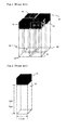
- FIG. 1 is a view schematically illustrating an image sensor using the BSI scheme described above, wherein four unit pixels constituted by red, green, and blue color filters 11, 21, 31 and 41, and by photodiodes 12, 22, 32 and 42 are shown in three dimensions.
- FIG. 2 is a view separating and illustrating only a red pixel from among the pixels. It should be noted that FIGs. 1 to 3 show an embodiment for only a color filter part of pixels included in an image sensor and only a photodiode part formed on a semiconductor substrate.
- the pixels in an image sensor using a BSI scheme have been smaller to a degree that the width thereof is 1.1 ⁇ m while the depth thereof is 3 to 5 ⁇ m, as shown in FIG. 2 , which makes it possible to integrate more pixels per unit area.
- a signal disturbance phenomenon which was not serious before, is raised as a new problem.
- FIG. 3 is a cross-sectional view of two pixels which are successively disposed.
- light incidented through a green color filter 21 generates photoelectrons in a corresponding photodiode 22.
- Most of the photoelectrons are normally captured in the depletion region (a portion shown as a dotted line in FIG. 3 ) of the photodiode 22 connected to the green color filter 21, and become useful current components.
- a part of the photoelectrons cross over into a photodiode 12 of an adjacent pixel, wherein as the width of the photodiodes 12 and 22 are narrower, the amount of photoelectrons crossing over into the photodiode 12 increases.
- Such photoelectrons are signal losses from the viewpoint of the photodiode 22 connected to the green color filter 21, and are unnecessary signals, i.e. color noise, from the viewpoint of the photodiode 12 connected to the red color filter 11.
- This is called a cross-talk phenomenon. Consequently, in pixels that the width thereof is as narrow as 1.1 ⁇ m while the depth thereof reaches 3 to 5 ⁇ m, the cross-talk phenomenon becomes serious, so that the advantage of the BSI scheme does not appear any more.
- a substrate may be manufactured to be thin to a thickness of a half or less (e.g. from 4 ⁇ m to 2 ⁇ m) in order to reduce the cross-talk phenomenon.
- incident light is not sufficiently absorbed by a silicon photodiode, and a transmittance of passing through the photodiode increases. That is to say, the quantum efficiency (QE) decreases to reduce the amplitude of an electric signal.
- the quantum efficiency (QE) means a ratio between incident light, i.e. incident photons, and electric charges generated/captured therefrom, and is an index representing how much efficiently light signals are converted into electric signals by an image sensor.
- the thickness thereof may be reduced in order to reduce the cross-talk phenomenon.
- green light is partially absorbed by the photodiode of a first substrate although blue light is mostly absorbed by the photodiode; and red light is absorbed by a smaller amount than the green light although the red light also is partially absorbed.
- infrared light shows a tendency to be absorbed by a smaller amount than the red light.
- an object of the present invention is to provide a substrate-stacked image sensor having a dual detection function which does not cause a cross talk while having a high quantum efficiency.
- Another object of the present invention is to provide a substrate-stacked image sensor having a function of doubly detecting incident light by: disposing a first photodiode on a first substrate; disposing a second photodiode on a second substrate; and coupling the first photodiode and the second photodiode to each other at the same time as the substrates are coupled to each other so as to be a complete photodiode as a component of one pixel.
- a substrate-stacked image sensor having a dual detection function, the senor comprising: a first photodiode formed on a first substrate; and a second photodiode formed on a second substrate, wherein the first photodiode and the second photodiode are in electric contact with each other.
- a substrate-stacked image sensor having a dual detection function, the senor comprising: a first photodiode and a first pad formed on a first substrate; and a second photodiode and a second pad formed on a second substrate, wherein the first photodiode and the second photodiode are electrically coupled to each other by contact of the first pad and the second pad.
- a substrate-stacked image sensor having a dual detection function, the senor comprising: a first photodiode and a first transfer transistor formed on a first substrate; and a second photodiode and a second transfer transistor formed on a second substrate, wherein the first photodiode, the second photodiode, the first transfer transistor, and the second transfer transistor are in electric contact with each other.
- a substrate-stacked image sensor having a dual detection function, the senor comprising: a first photodiode and a first transfer transistor formed on a first substrate; and a second photodiode formed on a second substrate, wherein the first photodiode and the second photodiode are in electric contact with each other.
- a substrate-stacked image sensor having a dual detection function, the senor comprising: a first photodiode formed on a first substrate; and a second photodiode and a second transfer transistor formed on a second substrate, wherein the first photodiode and the second photodiode are in electric contact with each other.
- the substrate-stacked image sensors in accordance with the embodiments of the present invention, most of blue light, a part of green light and a part of red light are absorbed by a first photodiode of a first substrate; and an extremely small part of the blue light, the residual part of the green light, the residual part of the red light, and infrared light are absorbed by a second photodiode of a second substrate for the second time, so that the quantum efficiency increases, and waste of incident light is minimized.
- a relative distance of a subject finally captured as an image can be measured through: the chromatism of the respective three colors (i.e. green, blue and red) which the external lens has; the analysis of frequency components of a captured image on the respective three colors of the upper substrate; and the analysis of frequency components of a captured image on the respective three colors of the lower substrate, so that basic image data to restore a three-dimensional image can be produced.
- an external optical system i.e. an external lens
- the present invention can be utilized to generate a three-dimensional image in a scheme which is entirely different from that used in the conventional stereo camera to generate a three-dimensional image.
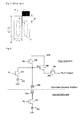
- FIG. 4 is a circuit diagram illustrating the technical idea of the present invention according to an embodiment of the present invention.
- one pixel includes one photodiode and four transistors. According to circumstances, one pixel may be constituted by one diode and three transistors. However, the number of transistors has no connection with the main idea of the present invention. Although a pixel includes several transistors, the characteristics of the present invention can be identically implemented.
- a second substrate has a second photodiode 212, a second transfer transistor 222, and a second pad 270.
- a first substrate has a first photodiode 211, a first transfer transistor 221, a reset transistor 230, a following transistor 240, a selection transistor 250, and a second pad 260.
- the first transfer transistor 221, the second transfer transistor 222, the reset transistor 230, the following transistor 240, and the selection transistor 250 function to output an electric signal converted by photodiodes as an output of a pixel, so that the transistors will be inclusively designated as "access transistors".
- Elements formed on the first substrate and elements formed on the second substrate are respectively manufactured by a well-known semiconductor manufacturing process, and then the two substrates are bonded with one of the two substrates turned over. In this case, the first pad and the second pad must be accurately aligned so as not to be out of line with each other.
- the main feature of the present invention is to form the first photodiode on the first substrate, to form the second photodiode on the second substrate, and then to electrically combine the first photodiode and second photodiode into one when bonding the substrates.
- the first transfer transistor 221 and the second transfer transistor 222 are also arranged on the two substrates, and are electrically combined into one when the substrates are bonded.
- the combination of transistors means that the gate node and drain node of one transistor are short-circuited to the gate node and drain node of the other transistor, respectively.
- a gate node signal TG for the respective transistors is applied in common.
- the current driving capability also increases by a width/length (W/L) ratio of each transistor.
- a circuit designer may preset the width/length (W/L) ratio of each transistor in consideration of the fact that the driving capability thereof increases by combination.
- gate node signals TG may be individually separated and controlled.
- the area which the first photodiode 211 occupies in the first substrate may be different from the area which the second photodiode 212 occupies in the second substrate. This is because not only the second photodiode 212 but also the other access transistors must be disposed on the same plane within a limited pixel area of the second substrate. Therefore, a pitch between some elements of a unit pixel formed on the first substrate is accurately identical to a pitch between the other elements of the unit pixel formed on the substrate.
- Fig. 5 representatively illustrates only a pixel corresponding to one of blue, green and red (BGR), which are three primary colors.
- Light incidented to an image sensor is incidented generally from the rear surface of the second substrate, is concentrated by a micro-lens, is individually selected by a color filter via a second buffer layer, passes through a first buffer layer, a P-type impurity region, and the like, and then arrives at a P-N junction region, which is a second photodiode 212.
- the order of the micro-lens, the second buffer layer, the first buffer layer, and the p-type impurity region are normal, and is not the main feature of the present invention, so a detailed description thereof will be omitted.
- the second substrate is disposed on the first substrate in the cross-sectional view of FIG. 5 .
- the other part of the remaining light is continuously transmitted to sufficiently arrive at the first photodiode 211. Accordingly, an extremely small part of remaining blue light, a part of remaining green light, and a part of remaining red light are converted into photoelectrons by the first photodiode 211 for the second time. That is to say, detection of light is doubly performed.
- photoelectrons converted by the first photodiode 211 may be more than those converted by the second photodiode 212 due to the high transmittance of the infrared light.
- the P-N junction region of the second photodiode 212 is wider than that of the first photodiode 211. This is because most access transistors must be additionally disposed on the first substrate while the first substrate and the second substrate must have the same pixel area.
- FIG. 5 illustrates only the first transfer transistor 221 on the first substrate for convenience sake, which is because all the access transistors may not be shown in one cross-section due to the disposition thereof although all the access transistors exist on the same plane.
- the P-N junction region of the second photodiode 212 may be narrower than the P-N junction region of the first substrate, which is one of various features shown in present invention.
- FIG. 6 is a circuit diagram schematically showing another embodiment of the present invention.
- the embodiment shown in FIG. 6 is the same as that shown in FIG. 4 except that a second transfer transistor does not exist, and only the second photodiode 212 and second pad 270 exist on the second substrate. Since only one transfer transistor 221 exists, it is impossible to select one of the first and second photodiodes 211 and 212, unlike the embodiment shown in FIG. 2 . According to the embodiment, only a photodiode can be disposed on the second substrate, without a transfer transistor and wirings for the transfer transistor, so that the area of the photodiode can be maximized.
- FIG. 7 is a circuit diagram schematically showing still another embodiment of the present invention.
- the first transfer transistor does not exist on a first substrate.
- two pads 280 and 290 are added for the electrical connections of the first photodiode 211 and second photodiode 212. Since the embodiment also includes only one transfer transistor 222, it is impossible to select one of the first and second photodiodes 211 and 212, unlike the embodiment shown in FIG. 4 .
- a transfer transistor and wirings for the transfer transistor are not required on the first substrate, and thus the area for the first photodiode can increase.
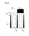
- FIG. 8 illustrates a case where a trench 87 is formed between the respective pixels in at least one of the first and second photodiodes according to the embodiments of the present invention, and the trench 87 is filled with impermeable material. Accordingly, photoelectrons generated by passing through color filters 81 and 82 stay only in the insides of the respective photodiodes 85 and 86, and can be prevented from crossing over into an adjacent photodiode. That is to say, the cross-talk phenomenon between pixels can be reduced.
Landscapes
- Engineering & Computer Science (AREA)
- Multimedia (AREA)
- Signal Processing (AREA)
- Solid State Image Pick-Up Elements (AREA)
- Transforming Light Signals Into Electric Signals (AREA)
- Facsimile Heads (AREA)
Abstract
Description
- The present invention relates to a substrate stacked image sensor wherein a pixel is completed by forming partial configurations of an image sensor pixel on mutually different substrates, respectively, and three-dimensionally stacking and bonding the substrates; and more particularly, to a substrate-stacked image sensor having a dual detection function wherein a first photodiode is disposed on a first substrate, a second photodiode is disposed on a second substrate, and the first photodiode and the second photodiode are coupled to form a complete photodiode as a configuration element of one pixel when the substrates are stacked and coupled to each other, and wherein the substrate-stacked image sensor can be controlled to selectively read or aggregately read signals individually detected by the respective photodiodes, as necessary.
- Background art may be described from two points of view. One is from the viewpoint of stacking of a semiconductor integrated circuit, and the other is from the viewpoint of miniaturization of an image sensor.
- Hereinafter, the conventional techniques on stacking of a semiconductor integrated circuit will be described. As semiconductor integrated circuits are continuously miniaturized, packaging techniques for semiconductor integrated circuits have also been continuously developed to satisfy demands for miniaturization and mounting reliability thereof. Recently, various techniques have been developed for substrate stacking with a three-dimensional (3D) structure in which two or more semiconductor chips or semiconductor packages are vertically stacked.
- A three-dimensional (3D) structure element using such substrate stacking is manufactured in such a manner that, after substrates are stacked, the stacked substrates are subjected to a thinning process of grinding the rear surface thereof to reduce the thickness thereof, are subjected to the following processes, are subjected to a sawing process, and then are packaged.
- There are very many conventional techniques for stacking substrates in various fields. The present applicant has also tried to develop various techniques. For example, a method for achieving more economic manufacture by omitting an etching process after bonding and stacking substrates is filed by the present applicant and assigned in Korean Patent Application No.
2010-0015632 (February 02, 2010 - In addition, a technique for minimizing the misalignment of bonding pads on the respective substrates when the substrates are bonded with each other is filed by the present applicant and assigned in Korean Patent Application No.
2010-0046400 (May 18, 2010 - In addition, a manufacturing method in which pads are more protruded on the respective substrates in order to facilitate bonding when stacking the substrates is also disclosed in Korean Patent Application No.
2010-53959 (June 08, 2010 - Considering the prior art from the viewpoint of miniaturization of an image sensor, with the development of mobile devices such as portable phones, it is necessary for a camera module built therein to have a lower height and for an image sensor included in a camera module to have a higher resolution in order to increase design flexibility in the mobile devices. By such a tendency, the size of pixels in an image sensor has also continuously decreased.
- Recently, with the development of the semiconductor integrated circuit technology, pixels have been able to be manufactured to have a size of approximately 1.4 µm x 1.4 µm which approximates to the wavelength band of visible light. Accordingly, in the case of the conventional front side illumination (FSI) scheme, a phenomenon in which light incidented from an exterior is not sufficiently concentrated to a photodiode due to obstacle of metal wirings disposed on the pixels significantly occurs. In order to solve such a problem, an image sensor using a back side illumination (BSI) scheme in which a photodiode is disposed as near as possible to an incident direction of light has been highlighted.
-
FIG. 1 is a view schematically illustrating an image sensor using the BSI scheme described above, wherein four unit pixels constituted by red, green, andblue color filters photodiodes FIG. 2 is a view separating and illustrating only a red pixel from among the pixels. It should be noted thatFIGs. 1 to 3 show an embodiment for only a color filter part of pixels included in an image sensor and only a photodiode part formed on a semiconductor substrate. - With the continuous development of the semiconductor technology, the pixels in an image sensor using a BSI scheme have been smaller to a degree that the width thereof is 1.1 µm while the depth thereof is 3 to 5 µm, as shown in
FIG. 2 , which makes it possible to integrate more pixels per unit area. In this case, a signal disturbance phenomenon, which was not serious before, is raised as a new problem. - Such a problem will be described in more detail with reference to
FIG. 3 , which is a cross-sectional view of two pixels which are successively disposed. InFIG. 3 , light incidented through agreen color filter 21 generates photoelectrons in acorresponding photodiode 22. Most of the photoelectrons are normally captured in the depletion region (a portion shown as a dotted line inFIG. 3 ) of thephotodiode 22 connected to thegreen color filter 21, and become useful current components. However, a part of the photoelectrons cross over into aphotodiode 12 of an adjacent pixel, wherein as the width of thephotodiodes photodiode 12 increases. Such photoelectrons are signal losses from the viewpoint of thephotodiode 22 connected to thegreen color filter 21, and are unnecessary signals, i.e. color noise, from the viewpoint of thephotodiode 12 connected to thered color filter 11. This is called a cross-talk phenomenon. Consequently, in pixels that the width thereof is as narrow as 1.1 µm while the depth thereof reaches 3 to 5 µm, the cross-talk phenomenon becomes serious, so that the advantage of the BSI scheme does not appear any more. - In a state where pixels have a size (i.e. interval) of 1.1 µm, a substrate may be manufactured to be thin to a thickness of a half or less (e.g. from 4 µm to 2 µm) in order to reduce the cross-talk phenomenon. However, in this case, incident light is not sufficiently absorbed by a silicon photodiode, and a transmittance of passing through the photodiode increases. That is to say, the quantum efficiency (QE) decreases to reduce the amplitude of an electric signal. Here, the quantum efficiency (QE) means a ratio between incident light, i.e. incident photons, and electric charges generated/captured therefrom, and is an index representing how much efficiently light signals are converted into electric signals by an image sensor.
- Also, in the conventional back side illumination-type image sensor, the thickness thereof may be reduced in order to reduce the cross-talk phenomenon. However, in this case, it has been well known that: green light is partially absorbed by the photodiode of a first substrate although blue light is mostly absorbed by the photodiode; and red light is absorbed by a smaller amount than the green light although the red light also is partially absorbed. In addition, infrared light shows a tendency to be absorbed by a smaller amount than the red light.
- Consequently, absorbing light means that photons have been converted into electric charges. Thus, the problem that the quantum efficiency (QE) is lower in the order of blue light, green light, red light and infrared light becomes larger in the back side illumination-type image sensor. In addition, the components of non-absorbed light are absorbed by other parts, except for photodiodes, are scattered after a collision with metal wirings, or are transmitted deep into stacked substrates, so that light is wasted regardless of the quantum efficiency.
- Accordingly, the present invention has been made in an effort to solve the problems occurring in the related art, and an object of the present invention is to provide a substrate-stacked image sensor having a dual detection function which does not cause a cross talk while having a high quantum efficiency.
- Another object of the present invention is to provide a substrate-stacked image sensor having a function of doubly detecting incident light by: disposing a first photodiode on a first substrate; disposing a second photodiode on a second substrate; and coupling the first photodiode and the second photodiode to each other at the same time as the substrates are coupled to each other so as to be a complete photodiode as a component of one pixel.
- The object of the present invention is not limited to the aforementioned objects. Other objects and advantages of the present invention will be more apparent from the following description.
- In order to achieve the above object, according to one aspect of the present invention, there is provided a substrate-stacked image sensor having a dual detection function, the senor comprising: a first photodiode formed on a first substrate; and a second photodiode formed on a second substrate, wherein the first photodiode and the second photodiode are in electric contact with each other.
- According to another aspect of the present invention, there is provided a substrate-stacked image sensor having a dual detection function, the senor comprising: a first photodiode and a first pad formed on a first substrate; and a second photodiode and a second pad formed on a second substrate, wherein the first photodiode and the second photodiode are electrically coupled to each other by contact of the first pad and the second pad.
- According to still another aspect of the present invention, there is provided a substrate-stacked image sensor having a dual detection function, the senor comprising: a first photodiode and a first transfer transistor formed on a first substrate; and a second photodiode and a second transfer transistor formed on a second substrate, wherein the first photodiode, the second photodiode, the first transfer transistor, and the second transfer transistor are in electric contact with each other.
- According to still another aspect of the present invention, there is provided a substrate-stacked image sensor having a dual detection function, the senor comprising: a first photodiode and a first transfer transistor formed on a first substrate; and a second photodiode formed on a second substrate, wherein the first photodiode and the second photodiode are in electric contact with each other.
- According to still another aspect of the present invention, there is provided a substrate-stacked image sensor having a dual detection function, the senor comprising: a first photodiode formed on a first substrate; and a second photodiode and a second transfer transistor formed on a second substrate, wherein the first photodiode and the second photodiode are in electric contact with each other.
- According to the configurations of the substrate-stacked image sensors in accordance with the embodiments of the present invention, most of blue light, a part of green light and a part of red light are absorbed by a first photodiode of a first substrate; and an extremely small part of the blue light, the residual part of the green light, the residual part of the red light, and infrared light are absorbed by a second photodiode of a second substrate for the second time, so that the quantum efficiency increases, and waste of incident light is minimized.
- According to the embodiments of the present invention, since two photodiodes of upper and lower substrates are positioned at physically different distances from an external optical system (i.e. an external lens), a relative distance of a subject finally captured as an image can be measured through: the chromatism of the respective three colors (i.e. green, blue and red) which the external lens has; the analysis of frequency components of a captured image on the respective three colors of the upper substrate; and the analysis of frequency components of a captured image on the respective three colors of the lower substrate, so that basic image data to restore a three-dimensional image can be produced.
- The present invention can be utilized to generate a three-dimensional image in a scheme which is entirely different from that used in the conventional stereo camera to generate a three-dimensional image.
- The above objects, and other features and advantages of the present invention will become more apparent after a reading of the following detailed description taken in conjunction with the drawings, in which:
-
FIG. 1 is a view illustrating a cross-section of pixels of an image sensor in three dimensions; -
FIG. 2 is a view illustrating one pixel which is selected fromFIG. 1 , and the size of which is expressed; -
FIG. 3 is a view explaining a cross-talk phenomenon; -
FIG. 4 is a circuit diagram schematically illustrating the configuration of a substrate-stacked image sensor according to an embodiment of the present invention; -
FIG. 5 is a cross-sectional view illustrating a semiconductor substrate in which the circuit diagram shown inFIG. 4 has been implemented; -
FIG. 6 is a circuit diagram schematically illustrating the configuration of a substrate-stacked image sensor according to another embodiment of the present invention; -
FIG. 7 is a circuit diagram schematically illustrating the configuration of a substrate-stacked image sensor according to still another embodiment of the present invention; and -
FIG. 8 is a view illustrating a trench formed between the respective photodiodes according to an embodiment of the present invention. - Reference will now be made in greater detail to a preferred embodiment of the invention, an example of which is illustrated in the accompanying drawings. Wherever possible, the same reference numerals will be used throughout the drawings and the description to refer to the same or like parts.
-
FIG. 4 is a circuit diagram illustrating the technical idea of the present invention according to an embodiment of the present invention. For convenience of description, it is assumed that one pixel includes one photodiode and four transistors. According to circumstances, one pixel may be constituted by one diode and three transistors. However, the number of transistors has no connection with the main idea of the present invention. Although a pixel includes several transistors, the characteristics of the present invention can be identically implemented. - A second substrate has a
second photodiode 212, asecond transfer transistor 222, and asecond pad 270. A first substrate has afirst photodiode 211, afirst transfer transistor 221, areset transistor 230, a followingtransistor 240, aselection transistor 250, and asecond pad 260. - The
first transfer transistor 221, thesecond transfer transistor 222, thereset transistor 230, the followingtransistor 240, and theselection transistor 250 function to output an electric signal converted by photodiodes as an output of a pixel, so that the transistors will be inclusively designated as "access transistors". - Elements formed on the first substrate and elements formed on the second substrate are respectively manufactured by a well-known semiconductor manufacturing process, and then the two substrates are bonded with one of the two substrates turned over. In this case, the first pad and the second pad must be accurately aligned so as not to be out of line with each other.
- The main feature of the present invention is to form the first photodiode on the first substrate, to form the second photodiode on the second substrate, and then to electrically combine the first photodiode and second photodiode into one when bonding the substrates.
- The
first transfer transistor 221 and thesecond transfer transistor 222 are also arranged on the two substrates, and are electrically combined into one when the substrates are bonded. Here, "the combination of transistors" means that the gate node and drain node of one transistor are short-circuited to the gate node and drain node of the other transistor, respectively. Naturally, it means that a gate node signal TG for the respective transistors is applied in common. Thus, by such combination, the current driving capability also increases by a width/length (W/L) ratio of each transistor. In addition, naturally, a circuit designer may preset the width/length (W/L) ratio of each transistor in consideration of the fact that the driving capability thereof increases by combination. - Also, in order to selectively control the
first transfer transistor 221 and thesecond transfer transistor 222 according to necessity, gate node signals TG may be individually separated and controlled. - The area which the
first photodiode 211 occupies in the first substrate may be different from the area which thesecond photodiode 212 occupies in the second substrate. This is because not only thesecond photodiode 212 but also the other access transistors must be disposed on the same plane within a limited pixel area of the second substrate. Therefore, a pitch between some elements of a unit pixel formed on the first substrate is accurately identical to a pitch between the other elements of the unit pixel formed on the substrate. - Hereinafter, one embodiment of the present invention will be described in detail from another viewpoint with reference to the cross-sectional view of
FIG. 5 . - Naturally, color filters for individually separating blue light, green light and red light are individually configured.
Fig. 5 representatively illustrates only a pixel corresponding to one of blue, green and red (BGR), which are three primary colors. - Light incidented to an image sensor is incidented generally from the rear surface of the second substrate, is concentrated by a micro-lens, is individually selected by a color filter via a second buffer layer, passes through a first buffer layer, a P-type impurity region, and the like, and then arrives at a P-N junction region, which is a
second photodiode 212. The order of the micro-lens, the second buffer layer, the first buffer layer, and the p-type impurity region are normal, and is not the main feature of the present invention, so a detailed description thereof will be omitted. It should be noted that the second substrate is disposed on the first substrate in the cross-sectional view ofFIG. 5 . - In this case, most of the selected light when the light is blue light, a part of the selected light when the light is green light, and a part of the selected light when the light is red light are absorbed into the
second photodiode 212, and are converted into photoelectrons. - Although a part of the remaining light which has not been absorbed into the second photodiode is scattered by metal wirings, which are not shown, the other part of the remaining light is continuously transmitted to sufficiently arrive at the
first photodiode 211. Accordingly, an extremely small part of remaining blue light, a part of remaining green light, and a part of remaining red light are converted into photoelectrons by thefirst photodiode 211 for the second time. That is to say, detection of light is doubly performed. Especially, in the case of infrared light, photoelectrons converted by thefirst photodiode 211 may be more than those converted by thesecond photodiode 212 due to the high transmittance of the infrared light. - As described above, the P-N junction region of the
second photodiode 212 is wider than that of thefirst photodiode 211. This is because most access transistors must be additionally disposed on the first substrate while the first substrate and the second substrate must have the same pixel area.FIG. 5 illustrates only thefirst transfer transistor 221 on the first substrate for convenience sake, which is because all the access transistors may not be shown in one cross-section due to the disposition thereof although all the access transistors exist on the same plane. - If most of the access transistors are disposed on the second substrate, the P-N junction region of the
second photodiode 212 may be narrower than the P-N junction region of the first substrate, which is one of various features shown in present invention. -
FIG. 6 is a circuit diagram schematically showing another embodiment of the present invention. The embodiment shown inFIG. 6 is the same as that shown inFIG. 4 except that a second transfer transistor does not exist, and only thesecond photodiode 212 andsecond pad 270 exist on the second substrate. Since only onetransfer transistor 221 exists, it is impossible to select one of the first andsecond photodiodes FIG. 2 . According to the embodiment, only a photodiode can be disposed on the second substrate, without a transfer transistor and wirings for the transfer transistor, so that the area of the photodiode can be maximized. -
FIG. 7 is a circuit diagram schematically showing still another embodiment of the present invention. Referring toFIG. 7 , the first transfer transistor does not exist on a first substrate. It should be noted that twopads first photodiode 211 andsecond photodiode 212. Since the embodiment also includes only onetransfer transistor 222, it is impossible to select one of the first andsecond photodiodes FIG. 4 . According to the embodiment, a transfer transistor and wirings for the transfer transistor are not required on the first substrate, and thus the area for the first photodiode can increase. - Since a person skilled in the art can easily derive the cross-section views corresponding to
FIGs. 6 and 7 , the cross-section views thereof will be omitted. The same reference numerals as used inFIG. 4 are used inFIGs. 6 and 7 so that it can be easily understood that the same reference numerals represent the same constituent elements. -
FIG. 8 illustrates a case where atrench 87 is formed between the respective pixels in at least one of the first and second photodiodes according to the embodiments of the present invention, and thetrench 87 is filled with impermeable material. Accordingly, photoelectrons generated by passing throughcolor filters respective photodiodes - Although a preferred embodiment of the present invention has been described for illustrative purposes, those skilled in the art will appreciate that various modifications, additions and substitutions are possible, without departing from the scope and the spirit of the invention as disclosed in the accompanying claims.
Claims (13)
- A multi-substrate image sensor having a dual detection function, the senor comprising:a first photodiode formed on a first substrate; anda second photodiode formed on a second substrate,wherein the first photodiode and the second photodiode are in electric contact with each other.
- A multi-substrate image sensor having a dual detection function, the senor comprising:a first photodiode and a first pad formed on a first substrate; anda second photodiode and a second pad formed on a second substrate,wherein the first photodiode and the second photodiode are electrically coupled to each other by contact of the first pad and the second pad.
- The image sensor according to claim 1 or 2, wherein the first substrate and the second substrate are made of silicon (Si), germanium (Ge), or gallium arsenic (GaAs).
- The image sensor according to claim 1 or 2, wherein, on the second substrate, an entire or a part of access transistors are formed.
- The image sensor according to claim 1 or 2, wherein a transfer transistor is selectively formed on only one of the first and second substrates.
- The image sensor according to claim 1 or 2, wherein a first transfer transistor of access transistors is formed on the first substrate, and a second transfer transistor thereof is formed on the second substrate.
- The image sensor according to claim 1 or 2, wherein the first photodiode and the second photodiode are integrated by the contact to produce one complete photodiode in one pixel.
- The image sensor according to claim 1 or 2, wherein the first photodiode and the second photodiode are different from each other in the sizes of P-N junctions thereof.
- The image sensor according to claim 1 or 2, wherein at least one of the first and second photodiodes has a trench formed on a periphery thereof.
- The image sensor according to claim 9, wherein the trench is filled with impermeable material.
- A multi-substrate image sensor having a dual detection function, the senor comprising:a first photodiode and a first transfer transistor formed on a first substrate; anda second photodiode and a second transfer transistor formed on a second substrate,wherein the first photodiode, the second photodiode, the first transfer transistor, and the second transfer transistor are in electric contact with each other.
- A multi-substrate image sensor having a dual detection function, the senor comprising:a first photodiode and a first transfer transistor formed on a first substrate; anda second photodiode formed on a second substrate,wherein the first photodiode and the second photodiode are in electric contact with each other.
- A multi-substrate image sensor having a dual detection function, the senor comprising:a first photodiode formed on a first substrate; anda second photodiode and a second transfer transistor formed on a second substrate,wherein the first photodiode and the second photodiode are in electric contact with each other.
Applications Claiming Priority (2)
| Application Number | Priority Date | Filing Date | Title |
|---|---|---|---|
| KR1020110078512A KR101399338B1 (en) | 2011-08-08 | 2011-08-08 | stacking substrate image sensor with dual sensing |
| PCT/KR2012/006293 WO2013022269A2 (en) | 2011-08-08 | 2012-08-08 | Multi-substrate image sensor having a dual detection function |
Publications (2)
| Publication Number | Publication Date |
|---|---|
| EP2743985A2 true EP2743985A2 (en) | 2014-06-18 |
| EP2743985A4 EP2743985A4 (en) | 2015-07-15 |
Family
ID=47669076
Family Applications (1)
| Application Number | Title | Priority Date | Filing Date |
|---|---|---|---|
| EP12822070.4A Withdrawn EP2743985A4 (en) | 2011-08-08 | 2012-08-08 | MULTI-SUBSTRATE IMAGE SENSOR HAVING DOUBLE DETECTION FUNCTION |
Country Status (6)
| Country | Link |
|---|---|
| US (1) | US9337227B2 (en) |
| EP (1) | EP2743985A4 (en) |
| JP (1) | JP2014523148A (en) |
| KR (1) | KR101399338B1 (en) |
| CN (1) | CN103733342B (en) |
| WO (1) | WO2013022269A2 (en) |
Cited By (1)
| Publication number | Priority date | Publication date | Assignee | Title |
|---|---|---|---|---|
| FR3026227A1 (en) * | 2014-09-18 | 2016-03-25 | Commissariat Energie Atomique | DEVICE FOR ACQUIRING 3D IMAGES |
Families Citing this family (183)
| Publication number | Priority date | Publication date | Assignee | Title |
|---|---|---|---|---|
| US12027518B1 (en) | 2009-10-12 | 2024-07-02 | Monolithic 3D Inc. | 3D semiconductor devices and structures with metal layers |
| US11374118B2 (en) | 2009-10-12 | 2022-06-28 | Monolithic 3D Inc. | Method to form a 3D integrated circuit |
| US10157909B2 (en) | 2009-10-12 | 2018-12-18 | Monolithic 3D Inc. | 3D semiconductor device and structure |
| US10366970B2 (en) | 2009-10-12 | 2019-07-30 | Monolithic 3D Inc. | 3D semiconductor device and structure |
| US10910364B2 (en) | 2009-10-12 | 2021-02-02 | Monolitaic 3D Inc. | 3D semiconductor device |
| US10043781B2 (en) | 2009-10-12 | 2018-08-07 | Monolithic 3D Inc. | 3D semiconductor device and structure |
| US10354995B2 (en) | 2009-10-12 | 2019-07-16 | Monolithic 3D Inc. | Semiconductor memory device and structure |
| US10388863B2 (en) | 2009-10-12 | 2019-08-20 | Monolithic 3D Inc. | 3D memory device and structure |
| US11984445B2 (en) | 2009-10-12 | 2024-05-14 | Monolithic 3D Inc. | 3D semiconductor devices and structures with metal layers |
| US11018133B2 (en) | 2009-10-12 | 2021-05-25 | Monolithic 3D Inc. | 3D integrated circuit |
| US10217667B2 (en) | 2011-06-28 | 2019-02-26 | Monolithic 3D Inc. | 3D semiconductor device, fabrication method and system |
| US11482440B2 (en) | 2010-12-16 | 2022-10-25 | Monolithic 3D Inc. | 3D semiconductor device and structure with a built-in test circuit for repairing faulty circuits |
| US12362219B2 (en) | 2010-11-18 | 2025-07-15 | Monolithic 3D Inc. | 3D semiconductor memory device and structure |
| US8163581B1 (en) * | 2010-10-13 | 2012-04-24 | Monolith IC 3D | Semiconductor and optoelectronic devices |
| US10497713B2 (en) | 2010-11-18 | 2019-12-03 | Monolithic 3D Inc. | 3D semiconductor memory device and structure |
| US10896931B1 (en) | 2010-10-11 | 2021-01-19 | Monolithic 3D Inc. | 3D semiconductor device and structure |
| US11018191B1 (en) | 2010-10-11 | 2021-05-25 | Monolithic 3D Inc. | 3D semiconductor device and structure |
| US11257867B1 (en) | 2010-10-11 | 2022-02-22 | Monolithic 3D Inc. | 3D semiconductor device and structure with oxide bonds |
| US11469271B2 (en) | 2010-10-11 | 2022-10-11 | Monolithic 3D Inc. | Method to produce 3D semiconductor devices and structures with memory |
| US11600667B1 (en) | 2010-10-11 | 2023-03-07 | Monolithic 3D Inc. | Method to produce 3D semiconductor devices and structures with memory |
| US11315980B1 (en) | 2010-10-11 | 2022-04-26 | Monolithic 3D Inc. | 3D semiconductor device and structure with transistors |
| US11227897B2 (en) | 2010-10-11 | 2022-01-18 | Monolithic 3D Inc. | Method for producing a 3D semiconductor memory device and structure |
| US10290682B2 (en) | 2010-10-11 | 2019-05-14 | Monolithic 3D Inc. | 3D IC semiconductor device and structure with stacked memory |
| US11158674B2 (en) | 2010-10-11 | 2021-10-26 | Monolithic 3D Inc. | Method to produce a 3D semiconductor device and structure |
| US11024673B1 (en) | 2010-10-11 | 2021-06-01 | Monolithic 3D Inc. | 3D semiconductor device and structure |
| US10998374B1 (en) | 2010-10-13 | 2021-05-04 | Monolithic 3D Inc. | Multilevel semiconductor device and structure |
| US11855100B2 (en) | 2010-10-13 | 2023-12-26 | Monolithic 3D Inc. | Multilevel semiconductor device and structure with oxide bonding |
| US11929372B2 (en) | 2010-10-13 | 2024-03-12 | Monolithic 3D Inc. | Multilevel semiconductor device and structure with image sensors and wafer bonding |
| US11869915B2 (en) | 2010-10-13 | 2024-01-09 | Monolithic 3D Inc. | Multilevel semiconductor device and structure with image sensors and wafer bonding |
| US12094892B2 (en) | 2010-10-13 | 2024-09-17 | Monolithic 3D Inc. | 3D micro display device and structure |
| US11163112B2 (en) | 2010-10-13 | 2021-11-02 | Monolithic 3D Inc. | Multilevel semiconductor device and structure with electromagnetic modulators |
| US11164898B2 (en) | 2010-10-13 | 2021-11-02 | Monolithic 3D Inc. | Multilevel semiconductor device and structure |
| US11984438B2 (en) | 2010-10-13 | 2024-05-14 | Monolithic 3D Inc. | Multilevel semiconductor device and structure with oxide bonding |
| US10679977B2 (en) | 2010-10-13 | 2020-06-09 | Monolithic 3D Inc. | 3D microdisplay device and structure |
| US12080743B2 (en) | 2010-10-13 | 2024-09-03 | Monolithic 3D Inc. | Multilevel semiconductor device and structure with image sensors and wafer bonding |
| US11133344B2 (en) | 2010-10-13 | 2021-09-28 | Monolithic 3D Inc. | Multilevel semiconductor device and structure with image sensors |
| US11437368B2 (en) | 2010-10-13 | 2022-09-06 | Monolithic 3D Inc. | Multilevel semiconductor device and structure with oxide bonding |
| US10943934B2 (en) | 2010-10-13 | 2021-03-09 | Monolithic 3D Inc. | Multilevel semiconductor device and structure |
| US11043523B1 (en) | 2010-10-13 | 2021-06-22 | Monolithic 3D Inc. | Multilevel semiconductor device and structure with image sensors |
| US11404466B2 (en) | 2010-10-13 | 2022-08-02 | Monolithic 3D Inc. | Multilevel semiconductor device and structure with image sensors |
| US10978501B1 (en) | 2010-10-13 | 2021-04-13 | Monolithic 3D Inc. | Multilevel semiconductor device and structure with waveguides |
| US10833108B2 (en) | 2010-10-13 | 2020-11-10 | Monolithic 3D Inc. | 3D microdisplay device and structure |
| US12360310B2 (en) | 2010-10-13 | 2025-07-15 | Monolithic 3D Inc. | Multilevel semiconductor device and structure with oxide bonding |
| US11855114B2 (en) | 2010-10-13 | 2023-12-26 | Monolithic 3D Inc. | Multilevel semiconductor device and structure with image sensors and wafer bonding |
| US11063071B1 (en) | 2010-10-13 | 2021-07-13 | Monolithic 3D Inc. | Multilevel semiconductor device and structure with waveguides |
| US11605663B2 (en) | 2010-10-13 | 2023-03-14 | Monolithic 3D Inc. | Multilevel semiconductor device and structure with image sensors and wafer bonding |
| US11694922B2 (en) | 2010-10-13 | 2023-07-04 | Monolithic 3D Inc. | Multilevel semiconductor device and structure with oxide bonding |
| US11327227B2 (en) | 2010-10-13 | 2022-05-10 | Monolithic 3D Inc. | Multilevel semiconductor device and structure with electromagnetic modulators |
| US11854857B1 (en) | 2010-11-18 | 2023-12-26 | Monolithic 3D Inc. | Methods for producing a 3D semiconductor device and structure with memory cells and multiple metal layers |
| US11901210B2 (en) | 2010-11-18 | 2024-02-13 | Monolithic 3D Inc. | 3D semiconductor device and structure with memory |
| US11482438B2 (en) | 2010-11-18 | 2022-10-25 | Monolithic 3D Inc. | Methods for producing a 3D semiconductor memory device and structure |
| US12154817B1 (en) | 2010-11-18 | 2024-11-26 | Monolithic 3D Inc. | Methods for producing a 3D semiconductor memory device and structure |
| US11031275B2 (en) | 2010-11-18 | 2021-06-08 | Monolithic 3D Inc. | 3D semiconductor device and structure with memory |
| US11508605B2 (en) | 2010-11-18 | 2022-11-22 | Monolithic 3D Inc. | 3D semiconductor memory device and structure |
| US11804396B2 (en) | 2010-11-18 | 2023-10-31 | Monolithic 3D Inc. | Methods for producing a 3D semiconductor device and structure with memory cells and multiple metal layers |
| US11521888B2 (en) | 2010-11-18 | 2022-12-06 | Monolithic 3D Inc. | 3D semiconductor device and structure with high-k metal gate transistors |
| US11355381B2 (en) | 2010-11-18 | 2022-06-07 | Monolithic 3D Inc. | 3D semiconductor memory device and structure |
| US12272586B2 (en) | 2010-11-18 | 2025-04-08 | Monolithic 3D Inc. | 3D semiconductor memory device and structure with memory and metal layers |
| US12144190B2 (en) | 2010-11-18 | 2024-11-12 | Monolithic 3D Inc. | 3D semiconductor device and structure with bonding and memory cells preliminary class |
| US12033884B2 (en) | 2010-11-18 | 2024-07-09 | Monolithic 3D Inc. | Methods for producing a 3D semiconductor device and structure with memory cells and multiple metal layers |
| US11735462B2 (en) | 2010-11-18 | 2023-08-22 | Monolithic 3D Inc. | 3D semiconductor device and structure with single-crystal layers |
| US11862503B2 (en) | 2010-11-18 | 2024-01-02 | Monolithic 3D Inc. | Method for producing a 3D semiconductor device and structure with memory cells and multiple metal layers |
| US11004719B1 (en) | 2010-11-18 | 2021-05-11 | Monolithic 3D Inc. | Methods for producing a 3D semiconductor memory device and structure |
| US11923230B1 (en) | 2010-11-18 | 2024-03-05 | Monolithic 3D Inc. | 3D semiconductor device and structure with bonding |
| US11615977B2 (en) | 2010-11-18 | 2023-03-28 | Monolithic 3D Inc. | 3D semiconductor memory device and structure |
| US12125737B1 (en) | 2010-11-18 | 2024-10-22 | Monolithic 3D Inc. | 3D semiconductor device and structure with metal layers and memory cells |
| US11482439B2 (en) | 2010-11-18 | 2022-10-25 | Monolithic 3D Inc. | Methods for producing a 3D semiconductor memory device comprising charge trap junction-less transistors |
| US11121021B2 (en) | 2010-11-18 | 2021-09-14 | Monolithic 3D Inc. | 3D semiconductor device and structure |
| US11211279B2 (en) | 2010-11-18 | 2021-12-28 | Monolithic 3D Inc. | Method for processing a 3D integrated circuit and structure |
| US11443971B2 (en) | 2010-11-18 | 2022-09-13 | Monolithic 3D Inc. | 3D semiconductor device and structure with memory |
| US11784082B2 (en) | 2010-11-18 | 2023-10-10 | Monolithic 3D Inc. | 3D semiconductor device and structure with bonding |
| US11018042B1 (en) | 2010-11-18 | 2021-05-25 | Monolithic 3D Inc. | 3D semiconductor memory device and structure |
| US11164770B1 (en) | 2010-11-18 | 2021-11-02 | Monolithic 3D Inc. | Method for producing a 3D semiconductor memory device and structure |
| US12243765B2 (en) | 2010-11-18 | 2025-03-04 | Monolithic 3D Inc. | 3D semiconductor device and structure with metal layers and memory cells |
| US11355380B2 (en) | 2010-11-18 | 2022-06-07 | Monolithic 3D Inc. | Methods for producing 3D semiconductor memory device and structure utilizing alignment marks |
| US12136562B2 (en) | 2010-11-18 | 2024-11-05 | Monolithic 3D Inc. | 3D semiconductor device and structure with single-crystal layers |
| US11569117B2 (en) | 2010-11-18 | 2023-01-31 | Monolithic 3D Inc. | 3D semiconductor device and structure with single-crystal layers |
| US12100611B2 (en) | 2010-11-18 | 2024-09-24 | Monolithic 3D Inc. | Methods for producing a 3D semiconductor device and structure with memory cells and multiple metal layers |
| US12068187B2 (en) | 2010-11-18 | 2024-08-20 | Monolithic 3D Inc. | 3D semiconductor device and structure with bonding and DRAM memory cells |
| US11094576B1 (en) | 2010-11-18 | 2021-08-17 | Monolithic 3D Inc. | Methods for producing a 3D semiconductor memory device and structure |
| US11495484B2 (en) | 2010-11-18 | 2022-11-08 | Monolithic 3D Inc. | 3D semiconductor devices and structures with at least two single-crystal layers |
| US11107721B2 (en) | 2010-11-18 | 2021-08-31 | Monolithic 3D Inc. | 3D semiconductor device and structure with NAND logic |
| US11610802B2 (en) | 2010-11-18 | 2023-03-21 | Monolithic 3D Inc. | Method for producing a 3D semiconductor device and structure with single crystal transistors and metal gate electrodes |
| US12463076B2 (en) | 2010-12-16 | 2025-11-04 | Monolithic 3D Inc. | 3D semiconductor device and structure |
| US10388568B2 (en) | 2011-06-28 | 2019-08-20 | Monolithic 3D Inc. | 3D semiconductor device and system |
| US11735501B1 (en) | 2012-04-09 | 2023-08-22 | Monolithic 3D Inc. | 3D semiconductor device and structure with metal layers and a connective path |
| US10600888B2 (en) | 2012-04-09 | 2020-03-24 | Monolithic 3D Inc. | 3D semiconductor device |
| US11164811B2 (en) | 2012-04-09 | 2021-11-02 | Monolithic 3D Inc. | 3D semiconductor device with isolation layers and oxide-to-oxide bonding |
| US11694944B1 (en) | 2012-04-09 | 2023-07-04 | Monolithic 3D Inc. | 3D semiconductor device and structure with metal layers and a connective path |
| US11616004B1 (en) | 2012-04-09 | 2023-03-28 | Monolithic 3D Inc. | 3D semiconductor device and structure with metal layers and a connective path |
| US11476181B1 (en) | 2012-04-09 | 2022-10-18 | Monolithic 3D Inc. | 3D semiconductor device and structure with metal layers |
| US11594473B2 (en) | 2012-04-09 | 2023-02-28 | Monolithic 3D Inc. | 3D semiconductor device and structure with metal layers and a connective path |
| US11881443B2 (en) | 2012-04-09 | 2024-01-23 | Monolithic 3D Inc. | 3D semiconductor device and structure with metal layers and a connective path |
| US11088050B2 (en) | 2012-04-09 | 2021-08-10 | Monolithic 3D Inc. | 3D semiconductor device with isolation layers |
| US11410912B2 (en) | 2012-04-09 | 2022-08-09 | Monolithic 3D Inc. | 3D semiconductor device with vias and isolation layers |
| US12051674B2 (en) | 2012-12-22 | 2024-07-30 | Monolithic 3D Inc. | 3D semiconductor device and structure with metal layers |
| US11784169B2 (en) | 2012-12-22 | 2023-10-10 | Monolithic 3D Inc. | 3D semiconductor device and structure with metal layers |
| US11967583B2 (en) | 2012-12-22 | 2024-04-23 | Monolithic 3D Inc. | 3D semiconductor device and structure with metal layers |
| US11018116B2 (en) | 2012-12-22 | 2021-05-25 | Monolithic 3D Inc. | Method to form a 3D semiconductor device and structure |
| US11961827B1 (en) | 2012-12-22 | 2024-04-16 | Monolithic 3D Inc. | 3D semiconductor device and structure with metal layers |
| US11916045B2 (en) | 2012-12-22 | 2024-02-27 | Monolithic 3D Inc. | 3D semiconductor device and structure with metal layers |
| US11309292B2 (en) | 2012-12-22 | 2022-04-19 | Monolithic 3D Inc. | 3D semiconductor device and structure with metal layers |
| US11217565B2 (en) | 2012-12-22 | 2022-01-04 | Monolithic 3D Inc. | Method to form a 3D semiconductor device and structure |
| US11063024B1 (en) | 2012-12-22 | 2021-07-13 | Monlithic 3D Inc. | Method to form a 3D semiconductor device and structure |
| US10892169B2 (en) | 2012-12-29 | 2021-01-12 | Monolithic 3D Inc. | 3D semiconductor device and structure |
| US10651054B2 (en) | 2012-12-29 | 2020-05-12 | Monolithic 3D Inc. | 3D semiconductor device and structure |
| US11430667B2 (en) | 2012-12-29 | 2022-08-30 | Monolithic 3D Inc. | 3D semiconductor device and structure with bonding |
| US10903089B1 (en) | 2012-12-29 | 2021-01-26 | Monolithic 3D Inc. | 3D semiconductor device and structure |
| US10115663B2 (en) | 2012-12-29 | 2018-10-30 | Monolithic 3D Inc. | 3D semiconductor device and structure |
| US11177140B2 (en) | 2012-12-29 | 2021-11-16 | Monolithic 3D Inc. | 3D semiconductor device and structure |
| US11004694B1 (en) | 2012-12-29 | 2021-05-11 | Monolithic 3D Inc. | 3D semiconductor device and structure |
| US11430668B2 (en) | 2012-12-29 | 2022-08-30 | Monolithic 3D Inc. | 3D semiconductor device and structure with bonding |
| US11087995B1 (en) | 2012-12-29 | 2021-08-10 | Monolithic 3D Inc. | 3D semiconductor device and structure |
| US10600657B2 (en) | 2012-12-29 | 2020-03-24 | Monolithic 3D Inc | 3D semiconductor device and structure |
| US12249538B2 (en) | 2012-12-29 | 2025-03-11 | Monolithic 3D Inc. | 3D semiconductor device and structure including power distribution grids |
| US8902663B1 (en) | 2013-03-11 | 2014-12-02 | Monolithic 3D Inc. | Method of maintaining a memory state |
| US10325651B2 (en) | 2013-03-11 | 2019-06-18 | Monolithic 3D Inc. | 3D semiconductor device with stacked memory |
| US12094965B2 (en) | 2013-03-11 | 2024-09-17 | Monolithic 3D Inc. | 3D semiconductor device and structure with metal layers and memory cells |
| US11935949B1 (en) | 2013-03-11 | 2024-03-19 | Monolithic 3D Inc. | 3D semiconductor device and structure with metal layers and memory cells |
| US11869965B2 (en) | 2013-03-11 | 2024-01-09 | Monolithic 3D Inc. | 3D semiconductor device and structure with metal layers and memory cells |
| US11088130B2 (en) | 2014-01-28 | 2021-08-10 | Monolithic 3D Inc. | 3D semiconductor device and structure |
| US11923374B2 (en) | 2013-03-12 | 2024-03-05 | Monolithic 3D Inc. | 3D semiconductor device and structure with metal layers |
| US12100646B2 (en) | 2013-03-12 | 2024-09-24 | Monolithic 3D Inc. | 3D semiconductor device and structure with metal layers |
| US10840239B2 (en) | 2014-08-26 | 2020-11-17 | Monolithic 3D Inc. | 3D semiconductor device and structure |
| US11398569B2 (en) | 2013-03-12 | 2022-07-26 | Monolithic 3D Inc. | 3D semiconductor device and structure |
| US10224279B2 (en) | 2013-03-15 | 2019-03-05 | Monolithic 3D Inc. | Semiconductor device and structure |
| US11030371B2 (en) | 2013-04-15 | 2021-06-08 | Monolithic 3D Inc. | Automation for monolithic 3D devices |
| US11341309B1 (en) | 2013-04-15 | 2022-05-24 | Monolithic 3D Inc. | Automation for monolithic 3D devices |
| US11574109B1 (en) | 2013-04-15 | 2023-02-07 | Monolithic 3D Inc | Automation methods for 3D integrated circuits and devices |
| US9021414B1 (en) | 2013-04-15 | 2015-04-28 | Monolithic 3D Inc. | Automation for monolithic 3D devices |
| US11720736B2 (en) | 2013-04-15 | 2023-08-08 | Monolithic 3D Inc. | Automation methods for 3D integrated circuits and devices |
| US11270055B1 (en) | 2013-04-15 | 2022-03-08 | Monolithic 3D Inc. | Automation for monolithic 3D devices |
| US11487928B2 (en) | 2013-04-15 | 2022-11-01 | Monolithic 3D Inc. | Automation for monolithic 3D devices |
| KR101334219B1 (en) * | 2013-08-22 | 2013-11-29 | (주)실리콘화일 | An image sensor with 3d stacking structure |
| KR101530696B1 (en) * | 2013-10-04 | 2015-06-22 | (주)실리콘화일 | Image sensor approving spectral charateristic |
| JP6161522B2 (en) | 2013-11-20 | 2017-07-12 | オリンパス株式会社 | Image sensor |
| US11031394B1 (en) | 2014-01-28 | 2021-06-08 | Monolithic 3D Inc. | 3D semiconductor device and structure |
| US11107808B1 (en) | 2014-01-28 | 2021-08-31 | Monolithic 3D Inc. | 3D semiconductor device and structure |
| US10297586B2 (en) | 2015-03-09 | 2019-05-21 | Monolithic 3D Inc. | Methods for processing a 3D semiconductor device |
| US12094829B2 (en) | 2014-01-28 | 2024-09-17 | Monolithic 3D Inc. | 3D semiconductor device and structure |
| US9818779B2 (en) | 2014-03-27 | 2017-11-14 | Taiwan Semiconductor Manufacturing Co., Ltd. | CMOS image sensor structure |
| US20170237911A1 (en) * | 2014-11-06 | 2017-08-17 | Siliconfile Technologies Inc. | Image sensor having improved spectral characteristics |
| US11937422B2 (en) | 2015-11-07 | 2024-03-19 | Monolithic 3D Inc. | Semiconductor memory device and structure |
| US10825779B2 (en) | 2015-04-19 | 2020-11-03 | Monolithic 3D Inc. | 3D semiconductor device and structure |
| US12477752B2 (en) | 2015-09-21 | 2025-11-18 | Monolithic 3D Inc. | 3D semiconductor memory devices and structures |
| US10418369B2 (en) | 2015-10-24 | 2019-09-17 | Monolithic 3D Inc. | Multi-level semiconductor memory device and structure |
| US11114427B2 (en) | 2015-11-07 | 2021-09-07 | Monolithic 3D Inc. | 3D semiconductor processor and memory device and structure |
| US11114464B2 (en) | 2015-10-24 | 2021-09-07 | Monolithic 3D Inc. | 3D semiconductor device and structure |
| US12016181B2 (en) | 2015-10-24 | 2024-06-18 | Monolithic 3D Inc. | 3D semiconductor device and structure with logic and memory |
| US12615784B2 (en) | 2015-11-07 | 2026-04-28 | Monolithic 3D Inc. | 3D semiconductor memory device and structure |
| US12219769B2 (en) | 2015-10-24 | 2025-02-04 | Monolithic 3D Inc. | 3D semiconductor device and structure with logic and memory |
| US11978731B2 (en) | 2015-09-21 | 2024-05-07 | Monolithic 3D Inc. | Method to produce a multi-level semiconductor memory device and structure |
| US12035531B2 (en) | 2015-10-24 | 2024-07-09 | Monolithic 3D Inc. | 3D semiconductor device and structure with logic and memory |
| US10381328B2 (en) | 2015-04-19 | 2019-08-13 | Monolithic 3D Inc. | Semiconductor device and structure |
| US11296115B1 (en) | 2015-10-24 | 2022-04-05 | Monolithic 3D Inc. | 3D semiconductor device and structure |
| US10847540B2 (en) | 2015-10-24 | 2020-11-24 | Monolithic 3D Inc. | 3D semiconductor memory device and structure |
| US11011507B1 (en) | 2015-04-19 | 2021-05-18 | Monolithic 3D Inc. | 3D semiconductor device and structure |
| US11056468B1 (en) | 2015-04-19 | 2021-07-06 | Monolithic 3D Inc. | 3D semiconductor device and structure |
| US11956952B2 (en) | 2015-08-23 | 2024-04-09 | Monolithic 3D Inc. | Semiconductor memory device and structure |
| US10014333B2 (en) * | 2015-08-26 | 2018-07-03 | Semiconductor Components Industries, Llc | Back-side illuminated pixels with interconnect layers |
| US12250830B2 (en) | 2015-09-21 | 2025-03-11 | Monolithic 3D Inc. | 3D semiconductor memory devices and structures |
| DE112016004265T5 (en) | 2015-09-21 | 2018-06-07 | Monolithic 3D Inc. | 3D SEMICONDUCTOR DEVICE AND STRUCTURE |
| US12178055B2 (en) | 2015-09-21 | 2024-12-24 | Monolithic 3D Inc. | 3D semiconductor memory devices and structures |
| US12100658B2 (en) | 2015-09-21 | 2024-09-24 | Monolithic 3D Inc. | Method to produce a 3D multilayer semiconductor device and structure |
| US10522225B1 (en) | 2015-10-02 | 2019-12-31 | Monolithic 3D Inc. | Semiconductor device with non-volatile memory |
| US12120880B1 (en) | 2015-10-24 | 2024-10-15 | Monolithic 3D Inc. | 3D semiconductor device and structure with logic and memory |
| US11991884B1 (en) | 2015-10-24 | 2024-05-21 | Monolithic 3D Inc. | 3D semiconductor device and structure with logic and memory |
| KR102549621B1 (en) | 2016-09-02 | 2023-06-28 | 삼성전자주식회사 | Semiconductor device |
| US11251149B2 (en) | 2016-10-10 | 2022-02-15 | Monolithic 3D Inc. | 3D memory device and structure |
| US11329059B1 (en) | 2016-10-10 | 2022-05-10 | Monolithic 3D Inc. | 3D memory devices and structures with thinned single crystal substrates |
| US11812620B2 (en) | 2016-10-10 | 2023-11-07 | Monolithic 3D Inc. | 3D DRAM memory devices and structures with control circuits |
| US12225704B2 (en) | 2016-10-10 | 2025-02-11 | Monolithic 3D Inc. | 3D memory devices and structures with memory arrays and metal layers |
| US11711928B2 (en) | 2016-10-10 | 2023-07-25 | Monolithic 3D Inc. | 3D memory devices and structures with control circuits |
| US11930648B1 (en) | 2016-10-10 | 2024-03-12 | Monolithic 3D Inc. | 3D memory devices and structures with metal layers |
| US11869591B2 (en) | 2016-10-10 | 2024-01-09 | Monolithic 3D Inc. | 3D memory devices and structures with control circuits |
| JP6746476B2 (en) * | 2016-11-24 | 2020-08-26 | キヤノン株式会社 | Imaging device, imaging system, and moving body |
| FR3075462B1 (en) * | 2017-12-19 | 2020-03-27 | Commissariat A L'energie Atomique Et Aux Energies Alternatives | DEVICE FOR ACQUIRING A 2D IMAGE AND A DEPTH IMAGE OF A SCENE |
| US11158652B1 (en) | 2019-04-08 | 2021-10-26 | Monolithic 3D Inc. | 3D memory semiconductor devices and structures |
| US11296106B2 (en) | 2019-04-08 | 2022-04-05 | Monolithic 3D Inc. | 3D memory semiconductor devices and structures |
| US10892016B1 (en) | 2019-04-08 | 2021-01-12 | Monolithic 3D Inc. | 3D memory semiconductor devices and structures |
| US11763864B2 (en) | 2019-04-08 | 2023-09-19 | Monolithic 3D Inc. | 3D memory semiconductor devices and structures with bit-line pillars |
| US11018156B2 (en) | 2019-04-08 | 2021-05-25 | Monolithic 3D Inc. | 3D memory semiconductor devices and structures |
| US12317688B2 (en) * | 2021-05-08 | 2025-05-27 | Wuhan China Star Optoelectronics Technology Co., Ltd. | Display panel and display device with nanocrystalline particles that improve the light intensities of the light-emitting areas |
Family Cites Families (16)
| Publication number | Priority date | Publication date | Assignee | Title |
|---|---|---|---|---|
| KR100782463B1 (en) | 2005-04-13 | 2007-12-05 | (주)실리콘화일 | Separated unit pixel and its manufacturing method of an image sensor having a three-dimensional structure |
| KR100800310B1 (en) * | 2006-02-16 | 2008-02-01 | 마루엘에스아이 주식회사 | Optical sensing element capable of detecting visible light and infrared light and its manufacturing method |
| KR100835892B1 (en) * | 2007-03-26 | 2008-06-09 | (주)실리콘화일 | Chip Stacked Image Sensor |
| DE102007018014A1 (en) | 2007-04-17 | 2008-10-23 | Bayer Materialscience Ag | Heat integration in a Deacon process |
| US7888763B2 (en) | 2008-02-08 | 2011-02-15 | Omnivision Technologies, Inc. | Backside illuminated imaging sensor with improved infrared sensitivity |
| US7893468B2 (en) * | 2008-05-30 | 2011-02-22 | International Business Machines Corporation | Optical sensor including stacked photodiodes |
| US8471939B2 (en) * | 2008-08-01 | 2013-06-25 | Omnivision Technologies, Inc. | Image sensor having multiple sensing layers |
| US8054355B2 (en) * | 2008-10-16 | 2011-11-08 | Omnivision Technologies, Inc. | Image sensor having multiple sensing layers |
| KR20100046400A (en) | 2008-10-27 | 2010-05-07 | 엘지전자 주식회사 | Apparatus and method for displaying |
| KR101056141B1 (en) | 2008-11-13 | 2011-08-11 | 주식회사 다한이엔지 | PCB Laser Marking Device |
| KR20100076261A (en) * | 2008-12-26 | 2010-07-06 | 주식회사 동부하이텍 | Electro static discharge device of image sensor |
| KR101049083B1 (en) | 2009-04-10 | 2011-07-15 | (주)실리콘화일 | A unit pixel of an image sensor having a three-dimensional structure and a manufacturing method thereof |
| JP2010258157A (en) * | 2009-04-23 | 2010-11-11 | Panasonic Corp | Solid-state imaging device and manufacturing method thereof |
| KR101107627B1 (en) | 2010-02-22 | 2012-01-25 | (주)실리콘화일 | Pad Formation Method of Wafer with Three-Dimensional Structure |
| KR20110126891A (en) | 2010-05-18 | 2011-11-24 | (주)실리콘화일 | 3D image sensor and its manufacturing method |
| KR20110134139A (en) | 2010-06-08 | 2011-12-14 | (주)실리콘화일 | Manufacturing method of 3D structure image sensor |
-
2011
- 2011-08-08 KR KR1020110078512A patent/KR101399338B1/en active Active
-
2012
- 2012-08-08 EP EP12822070.4A patent/EP2743985A4/en not_active Withdrawn
- 2012-08-08 WO PCT/KR2012/006293 patent/WO2013022269A2/en not_active Ceased
- 2012-08-08 US US14/237,853 patent/US9337227B2/en active Active
- 2012-08-08 CN CN201280038912.7A patent/CN103733342B/en active Active
- 2012-08-08 JP JP2014524927A patent/JP2014523148A/en active Pending
Cited By (1)
| Publication number | Priority date | Publication date | Assignee | Title |
|---|---|---|---|---|
| FR3026227A1 (en) * | 2014-09-18 | 2016-03-25 | Commissariat Energie Atomique | DEVICE FOR ACQUIRING 3D IMAGES |
Also Published As
| Publication number | Publication date |
|---|---|
| US20140191357A1 (en) | 2014-07-10 |
| WO2013022269A3 (en) | 2013-06-13 |
| KR20130016518A (en) | 2013-02-18 |
| CN103733342A (en) | 2014-04-16 |
| US9337227B2 (en) | 2016-05-10 |
| KR101399338B1 (en) | 2014-05-30 |
| EP2743985A4 (en) | 2015-07-15 |
| CN103733342B (en) | 2016-10-19 |
| WO2013022269A2 (en) | 2013-02-14 |
| JP2014523148A (en) | 2014-09-08 |
Similar Documents
| Publication | Publication Date | Title |
|---|---|---|
| US9337227B2 (en) | Multi-substrate image sensor having a dual detection function | |
| US9520423B2 (en) | Image sensors including non-aligned grid patterns | |
| CN104106137B (en) | Board Stacked Image Sensor with Dual Detection | |
| KR102306670B1 (en) | image sensor and manufacturing method thereof | |
| US10455213B2 (en) | Device having a 2D image sensor and depth sensor | |
| KR20170036963A (en) | Semiconductor device and method for manufacturing the same | |
| CN102569328A (en) | Photosensitive imaging device and method for manufacturing semiconductor device | |
| US20140184864A1 (en) | Solid-state imaging device and electronic apparatus | |
| US12113084B2 (en) | Image sensor | |
| CN104701333B (en) | System image sensor package on three-dimensional chip | |
| US20240170525A1 (en) | Sensor device | |
| KR20100057302A (en) | Image sensor and method for manufacturing thereof | |
| JP2025522398A (en) | Image sensor and method for manufacturing the image sensor | |
| KR100723457B1 (en) | Semiconductor device | |
| CN222638997U (en) | Image sensors, electronic devices | |
| KR101305457B1 (en) | stacking substrate image sensor with dual sensing | |
| CN110491890B (en) | Semiconductor structure and method of forming the same | |
| KR20210028256A (en) | Multispectral image sensor and method for manufacturing image sensor | |
| EP3979322A1 (en) | Pixel structure and method for manufacturing a pixel structure | |
| KR101269681B1 (en) | Image sensor and method for manufacturing the same | |
| CN118693115A (en) | Image Sensor | |
| KR20120001338A (en) | Cmos image sensor including photo diode which has regions of diffrent refractive indices |
Legal Events
| Date | Code | Title | Description |
|---|---|---|---|
| PUAI | Public reference made under article 153(3) epc to a published international application that has entered the european phase |
Free format text: ORIGINAL CODE: 0009012 |
|
| 17P | Request for examination filed |
Effective date: 20140227 |
|
| AK | Designated contracting states |
Kind code of ref document: A2 Designated state(s): AL AT BE BG CH CY CZ DE DK EE ES FI FR GB GR HR HU IE IS IT LI LT LU LV MC MK MT NL NO PL PT RO RS SE SI SK SM TR |
|
| DAX | Request for extension of the european patent (deleted) | ||
| A4 | Supplementary search report drawn up and despatched |
Effective date: 20150616 |
|
| RIC1 | Information provided on ipc code assigned before grant |
Ipc: H04N 5/335 20110101ALI20150610BHEP Ipc: H01L 27/146 20060101AFI20150610BHEP Ipc: H04N 9/04 20060101ALI20150610BHEP Ipc: H04N 5/3745 20110101ALI20150610BHEP |
|
| 17Q | First examination report despatched |
Effective date: 20161014 |
|
| RAP1 | Party data changed (applicant data changed or rights of an application transferred) |
Owner name: SK HYNIX INC. |
|
| STAA | Information on the status of an ep patent application or granted ep patent |
Free format text: STATUS: THE APPLICATION IS DEEMED TO BE WITHDRAWN |
|
| 18D | Application deemed to be withdrawn |
Effective date: 20170225 |