JP6746476B2 - Imaging device, imaging system, and moving body - Google Patents
Imaging device, imaging system, and moving body Download PDFInfo
- Publication number
- JP6746476B2 JP6746476B2 JP2016228063A JP2016228063A JP6746476B2 JP 6746476 B2 JP6746476 B2 JP 6746476B2 JP 2016228063 A JP2016228063 A JP 2016228063A JP 2016228063 A JP2016228063 A JP 2016228063A JP 6746476 B2 JP6746476 B2 JP 6746476B2
- Authority
- JP
- Japan
- Prior art keywords
- signal
- substrate
- photoelectric conversion
- conversion unit
- output line
- Prior art date
- Legal status (The legal status is an assumption and is not a legal conclusion. Google has not performed a legal analysis and makes no representation as to the accuracy of the status listed.)
- Active
Links
- 238000003384 imaging method Methods 0.000 title claims description 70
- 239000000758 substrate Substances 0.000 claims description 261
- 238000006243 chemical reaction Methods 0.000 claims description 137
- 238000012545 processing Methods 0.000 claims description 59
- 238000000034 method Methods 0.000 claims description 12
- 239000004065 semiconductor Substances 0.000 description 42
- 230000003321 amplification Effects 0.000 description 34
- 238000003199 nucleic acid amplification method Methods 0.000 description 34
- 230000003287 optical effect Effects 0.000 description 23
- 239000011229 interlayer Substances 0.000 description 20
- 239000003990 capacitor Substances 0.000 description 18
- 238000012546 transfer Methods 0.000 description 12
- 230000006870 function Effects 0.000 description 11
- 230000005856 abnormality Effects 0.000 description 6
- 238000012935 Averaging Methods 0.000 description 5
- 238000001514 detection method Methods 0.000 description 5
- 238000010586 diagram Methods 0.000 description 4
- 230000000694 effects Effects 0.000 description 4
- 230000002159 abnormal effect Effects 0.000 description 2
- 238000004891 communication Methods 0.000 description 2
- 239000010410 layer Substances 0.000 description 2
- 230000007257 malfunction Effects 0.000 description 2
- 238000005259 measurement Methods 0.000 description 2
- 238000007781 pre-processing Methods 0.000 description 2
- 229910052710 silicon Inorganic materials 0.000 description 2
- 239000010703 silicon Substances 0.000 description 2
- 230000001133 acceleration Effects 0.000 description 1
- 238000003491 array Methods 0.000 description 1
- 230000004888 barrier function Effects 0.000 description 1
- 230000005540 biological transmission Effects 0.000 description 1
- 239000003086 colorant Substances 0.000 description 1
- 238000007796 conventional method Methods 0.000 description 1
- 238000012937 correction Methods 0.000 description 1
- 238000013144 data compression Methods 0.000 description 1
- 238000009792 diffusion process Methods 0.000 description 1
- 238000012986 modification Methods 0.000 description 1
- 230000004048 modification Effects 0.000 description 1
- 230000003071 parasitic effect Effects 0.000 description 1
- 238000005070 sampling Methods 0.000 description 1
- 230000035945 sensitivity Effects 0.000 description 1
Images


Classifications
-
- H—ELECTRICITY
- H01—ELECTRIC ELEMENTS
- H01L—SEMICONDUCTOR DEVICES NOT COVERED BY CLASS H10
- H01L27/00—Devices consisting of a plurality of semiconductor or other solid-state components formed in or on a common substrate
- H01L27/14—Devices consisting of a plurality of semiconductor or other solid-state components formed in or on a common substrate including semiconductor components sensitive to infrared radiation, light, electromagnetic radiation of shorter wavelength or corpuscular radiation and specially adapted either for the conversion of the energy of such radiation into electrical energy or for the control of electrical energy by such radiation
- H01L27/144—Devices controlled by radiation
- H01L27/146—Imager structures
- H01L27/14601—Structural or functional details thereof
- H01L27/14634—Assemblies, i.e. Hybrid structures
-
- H—ELECTRICITY
- H04—ELECTRIC COMMUNICATION TECHNIQUE
- H04N—PICTORIAL COMMUNICATION, e.g. TELEVISION
- H04N25/00—Circuitry of solid-state image sensors [SSIS]; Control thereof
- H04N25/60—Noise processing, e.g. detecting, correcting, reducing or removing noise
-
- H—ELECTRICITY
- H01—ELECTRIC ELEMENTS
- H01L—SEMICONDUCTOR DEVICES NOT COVERED BY CLASS H10
- H01L27/00—Devices consisting of a plurality of semiconductor or other solid-state components formed in or on a common substrate
- H01L27/14—Devices consisting of a plurality of semiconductor or other solid-state components formed in or on a common substrate including semiconductor components sensitive to infrared radiation, light, electromagnetic radiation of shorter wavelength or corpuscular radiation and specially adapted either for the conversion of the energy of such radiation into electrical energy or for the control of electrical energy by such radiation
- H01L27/144—Devices controlled by radiation
- H01L27/146—Imager structures
- H01L27/14601—Structural or functional details thereof
- H01L27/14636—Interconnect structures
-
- H—ELECTRICITY
- H01—ELECTRIC ELEMENTS
- H01L—SEMICONDUCTOR DEVICES NOT COVERED BY CLASS H10
- H01L27/00—Devices consisting of a plurality of semiconductor or other solid-state components formed in or on a common substrate
- H01L27/14—Devices consisting of a plurality of semiconductor or other solid-state components formed in or on a common substrate including semiconductor components sensitive to infrared radiation, light, electromagnetic radiation of shorter wavelength or corpuscular radiation and specially adapted either for the conversion of the energy of such radiation into electrical energy or for the control of electrical energy by such radiation
- H01L27/144—Devices controlled by radiation
- H01L27/146—Imager structures
- H01L27/14643—Photodiode arrays; MOS imagers
- H01L27/14645—Colour imagers
-
- H—ELECTRICITY
- H01—ELECTRIC ELEMENTS
- H01L—SEMICONDUCTOR DEVICES NOT COVERED BY CLASS H10
- H01L27/00—Devices consisting of a plurality of semiconductor or other solid-state components formed in or on a common substrate
- H01L27/14—Devices consisting of a plurality of semiconductor or other solid-state components formed in or on a common substrate including semiconductor components sensitive to infrared radiation, light, electromagnetic radiation of shorter wavelength or corpuscular radiation and specially adapted either for the conversion of the energy of such radiation into electrical energy or for the control of electrical energy by such radiation
- H01L27/144—Devices controlled by radiation
- H01L27/146—Imager structures
- H01L27/14643—Photodiode arrays; MOS imagers
- H01L27/14649—Infrared imagers
-
- H—ELECTRICITY
- H04—ELECTRIC COMMUNICATION TECHNIQUE
- H04N—PICTORIAL COMMUNICATION, e.g. TELEVISION
- H04N25/00—Circuitry of solid-state image sensors [SSIS]; Control thereof
- H04N25/70—SSIS architectures; Circuits associated therewith
- H04N25/71—Charge-coupled device [CCD] sensors; Charge-transfer registers specially adapted for CCD sensors
- H04N25/75—Circuitry for providing, modifying or processing image signals from the pixel array
-
- H—ELECTRICITY
- H04—ELECTRIC COMMUNICATION TECHNIQUE
- H04N—PICTORIAL COMMUNICATION, e.g. TELEVISION
- H04N25/00—Circuitry of solid-state image sensors [SSIS]; Control thereof
- H04N25/70—SSIS architectures; Circuits associated therewith
- H04N25/79—Arrangements of circuitry being divided between different or multiple substrates, chips or circuit boards, e.g. stacked image sensors
-
- B—PERFORMING OPERATIONS; TRANSPORTING
- B60—VEHICLES IN GENERAL
- B60Q—ARRANGEMENT OF SIGNALLING OR LIGHTING DEVICES, THE MOUNTING OR SUPPORTING THEREOF OR CIRCUITS THEREFOR, FOR VEHICLES IN GENERAL
- B60Q9/00—Arrangement or adaptation of signal devices not provided for in one of main groups B60Q1/00 - B60Q7/00, e.g. haptic signalling
-
- B—PERFORMING OPERATIONS; TRANSPORTING
- B60—VEHICLES IN GENERAL
- B60Y—INDEXING SCHEME RELATING TO ASPECTS CROSS-CUTTING VEHICLE TECHNOLOGY
- B60Y2400/00—Special features of vehicle units
- B60Y2400/30—Sensors
- B60Y2400/301—Sensors for position or displacement
- B60Y2400/3015—Optical cameras
-
- H—ELECTRICITY
- H01—ELECTRIC ELEMENTS
- H01L—SEMICONDUCTOR DEVICES NOT COVERED BY CLASS H10
- H01L27/00—Devices consisting of a plurality of semiconductor or other solid-state components formed in or on a common substrate
- H01L27/14—Devices consisting of a plurality of semiconductor or other solid-state components formed in or on a common substrate including semiconductor components sensitive to infrared radiation, light, electromagnetic radiation of shorter wavelength or corpuscular radiation and specially adapted either for the conversion of the energy of such radiation into electrical energy or for the control of electrical energy by such radiation
- H01L27/144—Devices controlled by radiation
- H01L27/146—Imager structures
- H01L27/14601—Structural or functional details thereof
- H01L27/1462—Coatings
- H01L27/14621—Colour filter arrangements
-
- H—ELECTRICITY
- H01—ELECTRIC ELEMENTS
- H01L—SEMICONDUCTOR DEVICES NOT COVERED BY CLASS H10
- H01L27/00—Devices consisting of a plurality of semiconductor or other solid-state components formed in or on a common substrate
- H01L27/14—Devices consisting of a plurality of semiconductor or other solid-state components formed in or on a common substrate including semiconductor components sensitive to infrared radiation, light, electromagnetic radiation of shorter wavelength or corpuscular radiation and specially adapted either for the conversion of the energy of such radiation into electrical energy or for the control of electrical energy by such radiation
- H01L27/144—Devices controlled by radiation
- H01L27/146—Imager structures
- H01L27/14601—Structural or functional details thereof
- H01L27/14625—Optical elements or arrangements associated with the device
- H01L27/14627—Microlenses
Description
本発明は撮像装置、撮像システム、および、移動体に関する。 The present invention relates to an imaging device, an imaging system, and a moving body.
特許文献1には、2つの基板を積層した撮像装置が開示されている。第1の基板に第1のフォトダイオードが形成され、第2の基板に第2のフォトダイオードが形成されている。2つのフォトダイオードは、2つのパッドを介して、電気的に接続されている。特許文献1は、このような構成により、高い量子効率を実現することができると述べている。
特許文献1に記載の撮像装置によれば、2つのフォトダイオードで生じた電荷は、それぞれ、画素の増幅部を構成するトランジスタの入力ノードに転送される。そして、当該入力ノードにおいて、転送された電荷が電圧信号に変換される。しかし、特許文献1の撮像装置においては、入力ノードが2つの基板の接続部、つまり、2つのパッドを含んでいる。そのため、入力ノードの容量が大きくなりやすい。結果として、電荷電圧変換効率が低下し、SN比が低下する可能性がある。
According to the imaging device described in
上記の課題に鑑み、本発明は、SN比を向上することが可能な撮像装置を提供することを目的とする。 In view of the above problems, it is an object of the present invention to provide an imaging device capable of improving the SN ratio.
本発明の1つの側面に係る実施例の撮像装置は、第1の光電変換部、および、前記第1の光電変換部で生じた電荷に基づく信号を出力する第1のトランジスタをそれぞれが含む複数の第1の画素の配された第1の基板と、第2の光電変換部、および、前記第2の光電変換部で生じた電荷に基づく信号を出力する第2のトランジスタをそれぞれが含む複数の第2の画素の配された第2の基板と、を備え、前記第1の基板と前記第2の基板とは間に絶縁膜を介して積層され、前記第1の基板と前記絶縁膜との界面に平行な面への前記第1の光電変換部の正射影と、前記面への前記第2の光電変換部の正射影とは、少なくとも部分的に重なり、前記第1のトランジスタの入力ノードと、前記第2のトランジスタの入力ノードとは、互いに電気的に分離されている。 An image pickup apparatus according to an embodiment of one aspect of the present invention includes a plurality of photoelectric conversion units each including a first photoelectric conversion unit and a first transistor that outputs a signal based on an electric charge generated in the first photoelectric conversion unit. A first substrate on which the first pixel is arranged, a second photoelectric conversion unit, and a plurality of second transistors each outputting a signal based on the charge generated in the second photoelectric conversion unit. And a second substrate on which the second pixel is arranged, the first substrate and the second substrate are laminated with an insulating film interposed therebetween, and the first substrate and the insulating film are provided. The orthographic projection of the first photoelectric conversion section on the plane parallel to the interface with and the orthographic projection of the second photoelectric conversion section on the plane at least partially overlap, and The input node and the input node of the second transistor are electrically isolated from each other.
本発明の別の側面に係る実施例の撮像装置は、第1の光電変換部、および、前記第1の光電変換部で生じた電荷に基づく信号を出力する第1のトランジスタをそれぞれが含む複数の第1の画素の配された第1の基板と、第2の光電変換部、および、前記第2の光電変換部で生じた電荷に基づく信号を出力する第2のトランジスタをそれぞれが含む複数の第2の画素の配された第2の基板と、を備え、前記第1の基板と前記第2の基板とは間に絶縁膜を介して積層され、前記第1の光電変換部に入射した入射光の一部が、前記第1の光電変換部を通過して、前記第2の基板の前記第2の光電変換部に入射し、前記第1のトランジスタの入力ノードと、前記第2のトランジスタの入力ノードとは、互いに電気的に分離されている。 An image pickup apparatus according to another embodiment of the present invention includes a plurality of first photoelectric conversion units, and a plurality of first transistors each of which outputs a signal based on an electric charge generated in the first photoelectric conversion unit. A first substrate on which the first pixel is arranged, a second photoelectric conversion unit, and a plurality of second transistors each outputting a signal based on the charge generated in the second photoelectric conversion unit. And a second substrate on which the second pixels are arranged, the first substrate and the second substrate are stacked with an insulating film interposed therebetween, and the second substrate is incident on the first photoelectric conversion unit. A part of the incident light that has passed through the first photoelectric conversion unit is incident on the second photoelectric conversion unit of the second substrate, and the input node of the first transistor and the second photoelectric conversion unit The input nodes of the transistors are electrically isolated from each other.
本発明によれば、SN比を向上することができる。 According to the present invention, the SN ratio can be improved.
[実施例1]
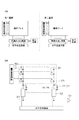
実施例1について説明する。図1は、実施例1に係る撮像装置の構成を模式的に示している。撮像装置は、第1の基板と第2の基板とを含む。図1(a)が、第1の基板および第2の基板のそれぞれの構成を模式的に示している。第1の基板および第2の基板のそれぞれが、画素アレイと、垂直走査回路、水平走査回路、列読み出し回路、および、出力回路などを含む信号処理回路とを含む。平面視において、換言すると、入射光の光軸に沿って見たときに、第1の基板の光電変換部と第2の基板の光電変換部とが互いに重なるように、第1の基板と第2の基板とが積層される。
[Example 1]
Example 1 will be described. FIG. 1 schematically illustrates the configuration of the image pickup apparatus according to the first embodiment. The imaging device includes a first substrate and a second substrate. FIG. 1A schematically shows the respective configurations of the first substrate and the second substrate. Each of the first substrate and the second substrate includes a pixel array, a vertical scanning circuit, a horizontal scanning circuit, a column reading circuit, and a signal processing circuit including an output circuit and the like. In plan view, in other words, when viewed along the optical axis of the incident light, the first substrate and the first substrate are arranged so that the photoelectric conversion unit of the first substrate and the photoelectric conversion unit of the second substrate overlap each other. Two substrates are stacked.
図1(b)は、第1の基板および第2の基板のそれぞれの画素アレイ、および、列読み出し回路、および、出力回路の構成を模式的に示している。図1(b)に関する説明は、第1の基板、および、第2の基板に対して共通である。 FIG. 1B schematically shows the configurations of the pixel arrays, the column readout circuit, and the output circuit of each of the first substrate and the second substrate. The description regarding FIG. 1B is common to the first substrate and the second substrate.
画素アレイ300は、複数の画素301を含む。複数の画素301は、複数の列および複数の行を成すように配置される。1つの列に属する複数の画素301が1つの列出力線106に接続される。1つの行に属する複数の画素301は、共通の制御線に接続される。制御線には、垂直走査回路からの制御信号が供給される。
The
列出力線106(206)には、電流源107(207)および列読み出し回路302が接続される。列読み出し回路302は、列出力線106または列出力線206に出力された信号に対して、信号処理を行う。列読み出し回路302の行う信号処理は、例えば、信号の保持、信号のサンプルホールド、信号の増幅、信号からのノイズ除去、信号に対するアナログデジタル変換(以下、AD変換)、複数の信号の加算、複数の信号の平均化を含む。列読み出し回路302は、これらの信号処理のいずれか1つを行ってもよいし、複数の信号処理を行ってもよい。
The current source 107 (207) and the
水平走査回路は、複数の列読み出し回路302からの信号を、順次、第2出力線303に出力する。出力回路304は、第2出力線303の信号を撮像装置の外部に出力する。
The horizontal scanning circuit sequentially outputs the signals from the plurality of
図2は、本実施例の画素301の等価回路を示す。本実施例の撮像装置は、第1の基板と第2の基板とに、それぞれ画素301を有する。第1の基板の画素301と第2の基板の画素301とは、同じ等価回路で示される。
FIG. 2 shows an equivalent circuit of the
第1の基板の画素301は、光電変換部100、転送トランジスタ101、リセットトランジスタ102、増幅トランジスタ103、および、選択トランジスタ104を有している。光電変換部100は、例えば、フォトダイオードである。リセットトランジスタ102のドレインおよび増幅トランジスタ103のドレインは、電源VDDを供給する電源線に接続される。転送トランジスタ101は、光電変換部100で生じた信号電荷を浮遊拡散部105(以下、FD部105)へ転送する。FD部105は、増幅トランジスタ103のゲート電極に接続されている。増幅トランジスタ103と、列出力線106に接続された電流源107は、ソースフォロワ回路を構成する。このような構成により、増幅トランジスタ103は、FD部105の電圧に応じた出力を、選択トランジスタ104を介して、列出力線106へ出力する。つまり、FD部105は増幅トランジスタ103の入力ノードを構成する。リセットトランジスタ102は、増幅トランジスタ103のゲート、すなわちFD部105を、既定の電位(リセット電位)にリセットする。垂直走査回路(不図示)が、信号を出力する行を選択する。
The
第2の基板の画素301は、光電変換部200、転送トランジスタ201、リセットトランジスタ202、増幅トランジスタ203、および、選択トランジスタ204を有している。光電変換部200は、例えば、フォトダイオードである。リセットトランジスタ202のドレインおよび増幅トランジスタ203のドレインは、電源VDDを供給する電源線に接続される。転送トランジスタ201は、光電変換部200で生じた信号電荷をFD部205へ転送する。FD部205は、増幅トランジスタ203のゲート電極に接続されている。増幅トランジスタ203と、列出力線206に接続された電流源207は、ソースフォロワ回路を構成する。このような構成により、増幅トランジスタ203は、FD部205の電圧に応じた出力を、選択トランジスタ204を介して、列出力線206へ出力する。つまり、FD部205は増幅トランジスタ203の入力ノードを構成する。リセットトランジスタ202は、増幅トランジスタ203のゲート、すなわちFD部205を、既定の電位(リセット電位)にリセットする。垂直走査回路(不図示)が、信号を出力する行を選択する。
The
なお、便宜的に第1の基板の画素301に含まれる要素と、第2の基板の画素301に含まれる要素とに別の符号を付している。しかし、同じ名称の要素は、同じ機能を有する。
Note that, for convenience, different reference numerals are given to elements included in the
次に、撮像装置の断面構造を説明する。図3は、撮像装置の断面構造を模式的に示す。第1の基板は、シリコンなどで形成された半導体基板151と、半導体基板151の上に配された配線およびゲート電極を含む。第2の基板は、シリコンなどで形成された半導体基板251と、半導体基板251の上に配された配線およびゲート電極を含む。
Next, the cross-sectional structure of the imaging device will be described. FIG. 3 schematically shows a cross-sectional structure of the image pickup device. The first substrate includes a
第1の基板と第2の基板とは積層されている。図3の点線ABが2つの基板の接触面を表している。本実施例では、第1の基板および第2の基板が、それぞれ、配線を覆う層間絶縁膜152、および、層間絶縁膜252を含む。そして、第1の基板の層間絶縁膜152と第2の基板の層間絶縁膜252とが互いに接している。このような構成により、層間絶縁膜152および層間絶縁膜252により構成された絶縁膜を介して、第1の基板と第2の基板とが積層される。
The first substrate and the second substrate are laminated. The dotted line AB in FIG. 3 represents the contact surface of the two substrates. In this embodiment, the first substrate and the second substrate each include an
図3は、第1の基板の上に配された配線として列出力線106、および、第2の基板の上に配された配線として列出力線206を示している。列出力線106および列出力線206は、半導体基板151と半導体基板251との間に配されている。列出力線106と半導体基板151とはコンタクトプラグを介して接続され、一方で、列出力線106の一部と半導体基板151の一部との間には層間絶縁膜152の一部が配される。列出力線206と半導体基板251とはコンタクトプラグを介して接続され、一方で、列出力線206の一部と半導体基板251の一部との間には層間絶縁膜252の一部が配される。
FIG. 3 shows
また、光が入射する面に、マイクロレンズMLおよびカラーフィルタCFなどの光学部材が配される。本実施例では、第1の基板に光が入射する。そのため、第1の基板にだけ、マイクロレンズMLおよびカラーフィルタCFが配される。しかし、第2の基板にも、マイクロレンズMLおよびカラーフィルタCFなどの光学部材が配されてもよい。 Further, optical members such as the microlenses ML and the color filters CF are arranged on the surface on which the light is incident. In this embodiment, light is incident on the first substrate. Therefore, the microlens ML and the color filter CF are arranged only on the first substrate. However, the second substrate may also be provided with optical members such as the microlenses ML and the color filters CF.
半導体基板151には、光電変換部100を構成する半導体領域が配される。半導体基板251には、光電変換部200を構成する半導体領域が配される。半導体基板151、および、半導体基板251には、それぞれ、トランジスタのソースまたはドレインあるいはFD部を構成する半導体領域(図3の105、110、205、210)が配される。また、半導体基板151、および、半導体基板251には、それぞれ、半導体領域を互いに分離するための分離部111および分離部211が配される。
A semiconductor region that constitutes the
本実施例においては、平面視において、第1の基板の画素301に含まれる光電変換部100と、第2の基板の画素301に含まれる光電変換部200とが、少なくとも部分的に重なる。平面とは、例えば、半導体基板151と層間絶縁膜152との界面に平行な面である。つまり、光電変換部100の当該界面に平行な面へ正射影と、光電変換部200の当該界面に平行な面へ正射影とが、少なくとも部分的に重なる。正射影とは、法線に沿った射影を意味する。
In the present embodiment, the
別の観点では、入射光の光軸に沿った方向で見たときに、第1の基板の画素301に含まれる光電変換部100と、第2の基板の画素301に含まれる光電変換部200とが、少なくとも部分的に重なる。図3は入射光の光軸Oを示している。光軸Oは、例えば、入射面に対する法線である。図3が示すように、断面で見たときに、入射光の光軸Oが光電変換部100と光電変換部200との両方を通過する。半導体基板151と層間絶縁膜152との界面が平坦ではない実施例では、このように光軸に沿って光電変換部100と光電変換部200とが配列される。
From another viewpoint, when viewed in a direction along the optical axis of incident light, the
入射光の光軸に沿って見たときに、光電変換部100の形と光電変換部200の形とが互いに一致していてもよい。あるいは、光電変換部100および光電変換部200の一方が他方を内包していてもよい。あるいは、光電変換部100の一部が、光電変換部200の一部と重なっていてもよい。
The shape of the
撮像装置に入射した光の一部は、第1の基板の画素301に含まれる光電変換部100において電荷に変換される。光電変換部100を通過した光は、第2の基板の画素301に含まれる光電変換部200に入射し、そして、光電変換部200において電荷に変換される。このように、入射光の一部が光電変換部100で電荷に変換され、入射光の別の一部が光電変換部200で電荷に変換される。これらの電荷は、それぞれ、第1の基板の画素301に含まれる増幅トランジスタ103と、第2の基板の画素301に含まれる増幅トランジスタ203とによって、互いに独立に読み出される。
Part of the light that has entered the imaging device is converted into electric charges in the
本実施例では、増幅トランジスタ103の入力ノード(FD部105)と、増幅トランジスタ203の入力ノード(FD部205)とは、互いに電気的に分離されている。換言すると、撮像装置は、増幅トランジスタ103の入力ノード(FD部105)と増幅トランジスタ203の入力ノード(FD部205)とがショートしていない状態を持つ。そのため、FD部105の容量およびFD部205の容量を小さくすることが可能である。
In this embodiment, the input node of the amplification transistor 103 (FD section 105) and the input node of the amplification transistor 203 (FD section 205) are electrically isolated from each other. In other words, the imaging device has a state in which the input node of the amplification transistor 103 (FD unit 105) and the input node of the amplification transistor 203 (FD unit 205) are not short-circuited. Therefore, it is possible to reduce the capacity of the
光電変換部100と光電変換部200で光電変換された電荷は、それぞれ、FD部105及びFD部205で電圧信号に変換される。V=Q/Cの関係式にしたがって、容量が小さいほど、変換ゲインは高くなる。
The charges photoelectrically converted by the
光電変換部100と光電変換部200とがFD部を共有した場合、FD部の容量が大きくなりやすい。結果として、電圧信号の振幅は圧縮されてしまう。その場合、後段の回路でゲインを大きくかける必要があり、ノイズ成分も大きくなる。つまり、画質が低下する可能性がある。
When the
これに対し、本実施例では、光電変換部100と光電変換部200は、1つのFD部を共有していない。代わりに、光電変換部100と光電変換部200のそれぞれに対して、別個のFD部105及びFD部205が割り当てられる。そのため、より大きな振幅を持つ電圧信号が、増幅トランジスタに入力される。結果として、SN比を向上することが可能である。
On the other hand, in this embodiment, the
第1の基板の光電変換部100で生じた電荷に基づく信号(以下、第1の信号と呼ぶ)と、第2の基板の光電変換部200で生じた電荷に基づく信号(以下、第2の信号と呼ぶ)とは、例えば、異なる波長帯の光についての情報を持つ。第1の基板が入射面を持つため、第1の信号は相対的に短い波長の光についての情報を含み、第2の信号が相対的に長い波長の光についての情報を含む。カラーフィルタCFを設けないことにより、可視光の中で異なる色の光を個別に検知することができる。あるいは、可視光の中の所定の波長帯の光と、赤外光を透過するカラーフィルタCFを用いることで、可視光と赤外光とを個別に検知することができる。このような構成により、本実施例の撮像装置は、高精細にカラー画像を撮像することができる。あるいは、本実施例の撮像装置は、可視光による画像と赤外光による画像とを同時に取得することができる。これらの例では、第1の信号と第2の信号は同一の用途に用いられる。
A signal based on the charge generated in the
一方、第1の信号と第2の信号とが、互いに異なる用途に用いられてもよい。例えば、第1の信号を撮像に用い、第2の信号を焦点検出に用いることができる。他にも、例えば、第1の信号を撮像に用い、第2の信号をTOF(Time Of Flight)法による測距に用いることができる。このような構成により、本実施例の撮像装置は、撮像動作と、焦点検出などの撮像動作以外の動作とを同時に行うことができる。 On the other hand, the first signal and the second signal may be used for different purposes. For example, the first signal can be used for imaging and the second signal can be used for focus detection. In addition, for example, the first signal can be used for imaging and the second signal can be used for distance measurement by the TOF (Time Of Flight) method. With such a configuration, the image pickup apparatus of the present embodiment can simultaneously perform an image pickup operation and an operation other than the image pickup operation such as focus detection.
図1(a)が示すように、本実施例では、第1の基板と第2の基板とがそれぞれ信号処理回路を含んでいる。第1の基板の信号処理回路は、第1の基板の光電変換部100で生じた電荷に基づく信号(第1の信号)を処理する。第2の基板の信号処理回路は、第2の基板の光電変換部200で生じた電荷に基づく信号(第2の信号)を処理する。図1(a)に示された構成によれば、第1の信号と第2の信号とは、それぞれ、別の出力回路によって撮像装置の外部に出力される。
As shown in FIG. 1A, in the present embodiment, the first substrate and the second substrate each include a signal processing circuit. The signal processing circuit of the first substrate processes a signal (first signal) based on the charges generated in the
外部に出力された第1の信号および第2の信号が、外部の信号処理装置によって加算されてもよい。また、変形例として、撮像装置の内部で、第1の信号と第2の信号とが加算または平均化されてもよい。そのために、第1の基板の信号処理回路と第2の基板の信号処理回路とが電気的に接続されうる。2つの信号処理回路を接続する配線経路に、第1の基板の配線と第2の基板の配線とを接続する接続部が含まれる。例えば、列読み出し回路302がAD変換を行う場合には、デジタル信号を伝達する信号線の配線経路に接続部が含まれる。あるいは、列読み出し回路302がアナログの増幅回路を含む場合には、増幅されたアナログ信号を伝達する信号線の配線経路に接続部が含まれる。
The first signal and the second signal output to the outside may be added by an external signal processing device. As a modification, the first signal and the second signal may be added or averaged inside the imaging device. Therefore, the signal processing circuit of the first substrate and the signal processing circuit of the second substrate can be electrically connected. The wiring path that connects the two signal processing circuits includes a connecting portion that connects the wiring of the first substrate and the wiring of the second substrate. For example, when the
本実施例では、異なる基板で生じた2つの信号を加算または平均化することで、感度を向上させることができる。あるいは、本実施例では、異なる基板で生じた2つの信号を加算または平均化することで、従来技術では得ることができなかった新たな信号を取得することができる。 In this embodiment, the sensitivity can be improved by adding or averaging two signals generated on different substrates. Alternatively, in this embodiment, two signals generated on different substrates can be added or averaged to obtain a new signal that cannot be obtained by the conventional technique.
以上に説明した通り、本実施例では、増幅トランジスタ103の入力ノード(FD部105)と、増幅トランジスタ203の入力ノード(FD部205)とは、互いに電気的に分離されている。このような構成によれば、SN比を向上させることが可能である。
As described above, in this embodiment, the input node (FD unit 105) of the
[実施例2]
実施例2について説明する。実施例2の撮像装置は、信号処理回路の一部が第2の基板にのみ配されている点で、実施例1の撮像装置と異なる。そこで、以下では主として実施例1と異なる部分を説明し、実施例1と同様の部分についての説明を省略する。
[Example 2]
Example 2 will be described. The image pickup apparatus of the second embodiment is different from the image pickup apparatus of the first embodiment in that a part of the signal processing circuit is arranged only on the second substrate. Therefore, in the following, the parts different from the first embodiment will be mainly described, and the description of the same parts as the first embodiment will be omitted.
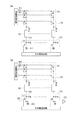
図4は、実施例2に係る撮像装置の構成を模式的に示している。撮像装置は、第1の基板と第2の基板とを含む。図4は、第1の基板および第2の基板のそれぞれの構成を模式的に示している。第1の基板および第2の基板のそれぞれが、画素アレイと、垂直走査回路とを含む。信号処理回路に含まれる水平走査回路、列読み出し回路、および、出力回路は、第2の基板だけに配されている。平面視において、換言すると、入射光の光軸に沿って見たときに、第1の基板の光電変換部と第2の基板の光電変換部とが互いに重なるように、第1の基板と第2の基板とが積層される。 FIG. 4 schematically illustrates the configuration of the image pickup apparatus according to the second embodiment. The imaging device includes a first substrate and a second substrate. FIG. 4 schematically shows the respective configurations of the first substrate and the second substrate. Each of the first substrate and the second substrate includes a pixel array and a vertical scanning circuit. The horizontal scanning circuit, the column reading circuit, and the output circuit included in the signal processing circuit are arranged only on the second substrate. In plan view, in other words, when viewed along the optical axis of the incident light, the first substrate and the first substrate are arranged so that the photoelectric conversion unit of the first substrate and the photoelectric conversion unit of the second substrate overlap each other. Two substrates are stacked.
図4は、さらに、第1の基板の配線と第2の基板の配線とを接続する接続部401を示している。第1の基板の列出力線106は、接続部401を介して、第2の基板に配された信号処理回路に接続されている。換言すると、第1の基板の列出力線106と第2の基板に配された信号処理回路とを接続する配線経路に、接続部401が含まれる。このような構成により、第1の基板と第2の基板とが、第2の基板に配された信号処理回路(水平走査回路、列読み出し回路、および、出力回路)を共有している。
FIG. 4 further shows a connecting
図5(a)は、第1の基板の信号処理回路の構成を模式的に示している。図1(b)の要素と同じ機能を有する部分には、図1(b)と同じ符号が付されている。図1(b)と同じ機能を有する要素については、図1(b)についての説明が全て適用される。 FIG. 5A schematically shows the configuration of the signal processing circuit on the first substrate. Portions having the same functions as those of the elements of FIG. 1B are designated by the same reference numerals as those of FIG. As for the elements having the same functions as those in FIG. 1B, all the description about FIG. 1B is applied.
図5(a)が示す通り、列出力線106は、電流源107および接続部401に接続される。第1の基板には、列読み出し回路302、水平走査回路、出力回路304が配されていない。
As shown in FIG. 5A, the
図5(b)は、第2の基板の信号処理回路の構成を模式的に示している。図1(b)の要素と同じ機能を有する部分には、図1(b)と同じ符号が付されている。図1(b)と同じ機能を有する要素については、図1(b)についての説明が全て適用される。 FIG. 5B schematically shows the configuration of the signal processing circuit of the second substrate. Portions having the same functions as those of the elements of FIG. 1B are designated by the same reference numerals as those of FIG. As for the elements having the same functions as those in FIG. 1B, all the description about FIG. 1B is applied.
本実施例においては、第1の基板の列出力線106、および、第2の基板の列出力線206が、1つの列読み出し回路302に接続される。第1の基板の列出力線106は、接続部401を介して、第2の基板に配された列読み出し回路302に接続される。列読み出し回路302は、列出力線106の信号と列出力線206の信号とを選択する選択手段を含んでいてもよい。
In this embodiment, the
本実施例の画素301の等価回路は、実施例1の画素301の等価回路と同じである。すなわち、図2は、本実施例の画素301の等価回路を示す。画素301の等価回路についての説明は省略する。
The equivalent circuit of the
次に、撮像装置の断面構造を説明する。図6は、撮像装置の断面構造を模式的に示す。図3に示された要素と同じ機能を有する部分には、図3と同じ符号を付してある。図3と同じ機能を持つ部分については、図3についての説明が全て適用される。 Next, the cross-sectional structure of the imaging device will be described. FIG. 6 schematically shows a cross-sectional structure of the image pickup device. Portions having the same functions as the elements shown in FIG. 3 are denoted by the same reference numerals as those in FIG. All the description about FIG. 3 is applied to the part having the same function as FIG.
第1の基板と第2の基板とは積層されている。図6の点線ABが2つの基板の接触面を表している。本実施例では、第1の基板および第2の基板が、それぞれ、配線を覆う層間絶縁膜152、および、層間絶縁膜252を含む。そして、第1の基板の層間絶縁膜152と第2の基板の層間絶縁膜252とが互いに接している。このような構成により、層間絶縁膜152および層間絶縁膜252により構成された絶縁膜を介して、第1の基板と第2の基板とが積層される。
The first substrate and the second substrate are laminated. The dotted line AB in FIG. 6 represents the contact surface of the two substrates. In this embodiment, the first substrate and the second substrate each include an
図6は、第1の基板の上に配された配線として列出力線106、および、第2の基板の上に配された配線として列出力線206を示している。列出力線106および列出力線206は、半導体基板151と半導体基板251との間に配されている。列出力線106と半導体基板151とはコンタクトプラグを介して接続され、一方で、列出力線106の一部と半導体基板151の一部との間には層間絶縁膜152の一部が配される。列出力線206と半導体基板251とはコンタクトプラグを介して接続され、一方で、列出力線206の一部と半導体基板251の一部との間には層間絶縁膜252の一部が配される。
FIG. 6 shows
半導体基板151には、光電変換部100を構成する半導体領域が配される。半導体基板251には、光電変換部200を構成する半導体領域が配される。半導体基板151、および、半導体基板251には、それぞれ、トランジスタのソースまたはドレインあるいはFD部を構成する半導体領域(図6の110、210)が配される。また、半導体基板151、および、半導体基板251には、それぞれ、半導体領域を互いに分離するための分離部111および分離部211が配される。
A semiconductor region that constitutes the
本実施例においては、平面視において、第1の基板の画素301に含まれる光電変換部100と、第2の基板の画素301に含まれる光電変換部200とが、少なくとも部分的に重なる。平面とは、例えば、半導体基板151と層間絶縁膜152との界面に平行な面である。つまり、光電変換部100の当該界面に平行な面へ正射影と、光電変換部200の当該界面に平行な面へ正射影とが、少なくとも部分的に重なる。正射影とは、法線に沿った射影を意味する。
In the present embodiment, the
別の観点では、入射光の光軸に沿った方向で見たときに、第1の基板の画素301に含まれる光電変換部100と、第2の基板の画素301に含まれる光電変換部200とが、少なくとも部分的に重なる。図6は入射光の光軸Oを示している。光軸Oは、例えば、入射面に対する法線である。図6が示すように、断面で見たときに、入射光の光軸Oが光電変換部100と光電変換部200との両方を通過する。半導体基板151と層間絶縁膜152との界面が平坦ではない実施例では、このように光軸に沿って光電変換部100と光電変換部200とが配列される。
From another point of view, when viewed in a direction along the optical axis of incident light, the
入射光の光軸に沿って見たときに、光電変換部100の形と光電変換部200の形とが互いに一致していてもよい。あるいは、光電変換部100および光電変換部200の一方が他方を内包していてもよい。あるいは、光電変換部100の一部が、光電変換部200の一部と重なっていてもよい。
The shape of the
撮像装置に入射した光の一部は、第1の基板の画素301に含まれる光電変換部100において電荷に変換される。光電変換部100を通過した光は、第2の基板の画素301に含まれる光電変換部200に入射し、そして、光電変換部200において電荷に変換される。このように、入射光の一部が光電変換部100で電荷に変換され、入射光の別の一部が光電変換部200で電荷に変換される。これらの電荷は、それぞれ、第1の基板の画素301に含まれる増幅トランジスタ103と、第2の基板の画素301に含まれる増幅トランジスタ203とによって、互いに独立に読み出される。
Part of the light that has entered the imaging device is converted into electric charges in the
本実施例では、第1の基板の列出力線106が、接続部401を介して、第2の基板の列読み出し回路302を構成するトランジスタに接続される。接続部401は、2層の配線が接触している構造を有している。このような構成により、第2の基板に配された信号処理回路は、第1の基板の光電変換部100で生じた電荷に基づく信号(以下、第1の信号と呼ぶ)と、第2の基板の光電変換部200で生じた電荷に基づく信号(以下、第2の信号と呼ぶ)との両方を処理する。具体的に、第2の基板に配された列読み出し回路302は、第1の信号に対して、信号の保持、信号のサンプルホールド、信号の増幅、信号からのノイズ除去、信号に対するAD変換、複数の信号の加算、複数の信号の平均化などの信号処理を行う。また、第2の基板に配された列読み出し回路302は、第2の信号に対して、信号の保持、信号のサンプルホールド、信号の増幅、信号からのノイズ除去、信号に対するAD変換、複数の信号の加算、複数の信号の平均化などの信号処理を行う。列読み出し回路302は、第1の信号と第2の信号とのどちらに対して信号処理を行うかを選択することができる。
In the present embodiment, the
図7は、本実施例の撮像装置の動作を模式的に示している。図7(a)に示された動作では、まず、第1の基板の画素アレイのうち、n行目の画素301の信号(第1の信号)が読み出される。次に、第2の基板の画素アレイのうち、n行目の画素301の信号(第2の信号)が読み出される。その後、第1の基板の画素アレイのうち、n+1行目の画素301の信号(別の第1の信号)が読み出される。以降、同様の読み出しが繰り返される。
FIG. 7 schematically shows the operation of the image pickup apparatus of this embodiment. In the operation shown in FIG. 7A, first, the signal (first signal) of the
ここで、n行目の第1の基板の読み出し時間には、各列の信号を水平転送する時間が含まれてもよい。さらには、列読み出し回路302のメモリ等に信号を保持することで、第1の信号の水平転送時間と、第2の信号の読み出し時間の一部とを重ねることができる。
Here, the readout time of the first substrate on the n-th row may include the time for horizontally transferring the signal of each column. Further, by holding the signal in the memory or the like of the
なお、図7(b)が示すように、第1の基板のn行目の画素301から第1の信号が読み出され、そのあとに、第2の基板のm行目(m≠n)の画素301から第2の信号が読み出されてもよい。
As shown in FIG. 7B, the first signal is read from the
第1の信号と第2の信号の用途は、実施例1と同様である。例えば、第1の信号と第2の信号とは、互いに異なる波長帯の光についての情報を持つ。あるいは、第1の信号と第2の信号とが、互いに異なる用途に用いられてもよい。 The uses of the first signal and the second signal are the same as in the first embodiment. For example, the first signal and the second signal have information about lights in different wavelength bands. Alternatively, the first signal and the second signal may be used for different applications.
本実施例においては、第2の基板に配された信号処理回路が、第1の基板の列出力線に出力された第1の信号と、第2の基板の列出力線206に出力された第2の信号との両方を処理する。このように、第1の信号の処理および第2の信号の処理に、共通の信号処理回路を使用することで、列読み出し回路302の数を減らすことができる。結果として、撮像装置のサイズを小さくすることが可能である。また、図7に示されるように、順次信号を読み出すことにより、消費電力を低減する効果が得られる。
In the present embodiment, the signal processing circuit arranged on the second substrate outputs the first signal output to the column output line of the first substrate and the
また、実施例1と同様に、本実施例では、増幅トランジスタ103の入力ノード(FD部105)と、増幅トランジスタ203の入力ノード(FD部205)とは、互いに電気的に分離されている。このような構成によれば、SN比を向上させることが可能である。
Further, similarly to the first embodiment, in the present embodiment, the input node (FD unit 105) of the
[実施例3]
実施例3について説明する。本実施例の撮像装置は、第1の基板と第2の基板とが出力回路304のみを共有している点で、実施例1の撮像装置、および、実施例2の撮像装置とことなる。そこで、以下では主として実施例1および実施例2と異なる部分を説明し、実施例1または実施例2と同様の部分についての説明を省略する。
[Example 3]
Example 3 will be described. The image pickup apparatus of the present embodiment is different from the image pickup apparatus of the first embodiment and the image pickup apparatus of the second embodiment in that the first substrate and the second substrate share only the
図8は、実施例3に係る撮像装置の構成を模式的に示している。撮像装置は、第1の基板と第2の基板とを含む。第1の基板および第2の基板のそれぞれが、画素アレイと、垂直走査回路と、列読み出し回路と、保持容量回路と、水平走査回路を含む。信号処理回路に含まれる出力回路は、第2の基板だけに配されている。平面視において、換言すると、入射光の光軸に沿って見たときに、第1の基板の光電変換部と第2の基板の光電変換部とが互いに重なるように、第1の基板と第2の基板とが積層される。 FIG. 8 schematically shows the configuration of the image pickup apparatus according to the third embodiment. The imaging device includes a first substrate and a second substrate. Each of the first substrate and the second substrate includes a pixel array, a vertical scanning circuit, a column reading circuit, a storage capacitor circuit, and a horizontal scanning circuit. The output circuit included in the signal processing circuit is arranged only on the second substrate. In plan view, in other words, when viewed along the optical axis of the incident light, the first substrate and the first substrate are arranged so that the photoelectric conversion unit of the first substrate and the photoelectric conversion unit of the second substrate overlap each other. Two substrates are stacked.
列読み出し回路302の後段に、保持容量回路313が接続される。保持容量回路313は、列読み出し回路302から出力された信号を保持する。水平走査回路は、保持容量回路313に保持された信号を、順次、第2出力線303に出力する。出力回路304は、第2出力線303の信号を撮像装置の外部に出力する。
The
図8は、さらに、第1の基板の配線と第2の基板の配線とを接続する接続部402を示している。第1の基板の保持容量回路313は、接続部402を介して、第2の基板に配された信号処理回路に接続されている。換言すると、第1の基板の保持容量回路313と第2の基板に配された信号処理回路とを接続する配線経路に、接続部402が含まれる。図視されていないが、接続部402は、2層の配線が接触している構造を有している。このような構成により、第1の基板と第2の基板とが、第2の基板に配された信号処理回路(出力回路)を共有している。
FIG. 8 further shows a connecting
図9(a)は、第1の基板の信号処理回路の構成を模式的に示している。図9(b)は、第2の基板の信号処理回路の構成を模式的に示している。図1(b)の要素と同じ機能を有する部分には、図1(b)と同じ符号が付されている。図1(b)と同じ機能を有する要素については、図1(b)についての説明が全て適用される。 FIG. 9A schematically shows the configuration of the signal processing circuit of the first substrate. FIG. 9B schematically shows the configuration of the signal processing circuit of the second substrate. Portions having the same functions as those of the elements of FIG. 1B are designated by the same reference numerals as those of FIG. As for the elements having the same functions as those in FIG. 1B, all the description about FIG. 1B is applied.
第1の基板に配された保持容量回路313、および、第2の基板に配された保持容量回路313は、それぞれ、容量素子306と転送スイッチ307とを含む。水平走査回路からの制御信号が、転送スイッチ307のゲートに入力される。第1の基板の転送スイッチ307は、容量素子306と接続部402とを接続する。そして、第1の基板の保持容量回路313は、接続部402を介して第2出力線303に接続される。第2の基板の転送スイッチ307は、容量素子306と第2出力線とを接続する。第2出力線303の信号は、出力回路304に入力される。
The holding
本実施例の画素301の等価回路は、実施例1の画素301の等価回路と同じである。すなわち、図2は、本実施例の画素301の等価回路を示す。画素301の等価回路についての説明は省略する。
The equivalent circuit of the
上述の通り、本実施例では、第1の基板と第2の基板とが、第2出力線および出力回路304を共有している。第2の基板に配された出力回路304は、第1の基板の光電変換部100で生じた電荷に基づく信号(第1の信号)と、第2の基板の光電変換部200で生じた電荷に基づく信号(第2の信号)とを、撮像装置の外部へ出力する。このような構成により、回路規模を小さくすることができ、消費電力の低減効果を得ることができる。
As described above, in this embodiment, the first substrate and the second substrate share the second output line and the
また、実施例1と同様に、本実施例では、増幅トランジスタ103の入力ノード(FD部105)と、増幅トランジスタ203の入力ノード(FD部205)とは、互いに電気的に分離されている。このような構成によれば、SN比を向上させることが可能である。
Further, similarly to the first embodiment, in the present embodiment, the input node (FD unit 105) of the
[実施例4]
実施例4について説明する。本実施例の撮像装置は、列読み出し回路302の機能および構成が異なる点を除いて、実施例2の撮像装置と同じである。そこで、以下では主として、実施例2と異なる部分を説明し、実施例2と同様の部分についての説明を適宜省略する。
[Example 4]
Example 4 will be described. The image pickup apparatus according to the present embodiment is the same as the image pickup apparatus according to the second embodiment except that the column read
本実施例に係る撮像装置の構成は、実施例2の撮像装置と同じである。すなわち、図4および図5は、本実施例の撮像装置の構成を模式的に示している。図4および図5についての説明は、全て本実施例に適用される。 The configuration of the image pickup apparatus according to the present embodiment is the same as that of the image pickup apparatus according to the second embodiment. That is, FIG. 4 and FIG. 5 schematically show the configuration of the image pickup apparatus of this embodiment. 4 and 5 are all applied to this embodiment.
本実施例の列読み出し回路302は、第1の基板の光電変換部100で生じた電荷に基づく信号(以下、第1の信号と呼ぶ)と、第2の基板の光電変換部200で生じた電荷に基づく信号(以下、第2の信号と呼ぶ)とを加算する。列読み出し回路302について、詳細に説明する。
In the
図10は、列読み出し回路302の等価回路を示す。列読み出し回路302は、第1容量素子800、第2容量素子801、オペアンプ802、帰還回路803、および、サンプルホールド回路804を含む。
FIG. 10 shows an equivalent circuit of the column read
第1の基板の列出力線106は、接続部401および第1容量素子800を介して、オペアンプ802の反転入力ノードに接続される。第1容量素子800の一端が接続部401に接続され、第1容量素子800の他端がオペアンプ802の反転入力ノードに接続される。第2の基板の列出力線206は、第2容量素子801を介して、オペアンプ802の反転入力ノードに接続される。第2容量素子801の一端が列出力線206に接続され、第2容量素子801の他端がオペアンプ802の反転入力ノードに接続される。オペアンプ802の非反転入力ノードには、所定の参照電圧が供給される。
The
帰還回路803は、帰還容量と、帰還容量へ直列に接続された帰還スイッチと、帰還容量に並列に接続されたリセットスイッチとを含む。帰還回路803は、オペアンプ802の出力ノードと反転入力ノードとの間に負帰還ループを形成する。サンプルホールド回路804は、サンプリングスイッチと保持容量素子と転送スイッチと、を含む
列読み出し回路302が加算を行うための動作を説明する。まず、リセットスイッチをオンすることで、オペアンプ802の反転入力ノードをリセットする。リセットスイッチをオフにした後に、帰還スイッチをオンにする。続いて、第1の信号と第2の信号とが、それぞれ、第1容量素子800と第2容量素子801に入力される。これにより、オペアンプ802は、第1の信号の振幅と第2の信号の振幅との和に相当する振幅を持つ信号を出力する。
The
図11は、本実施例の撮像装置の動作を模式的に表している。図11において、1つの読み出し期間として示された期間に、上述のオペアンプのリセットおよび第1の信号と第2の信号との加算が行われる。まず、第1の基板の画素アレイのうち、n行目の画素301の信号(第1の信号)が読み出される。同時に、第2の基板の画素アレイのうち、n行目の画素301の信号(第2の信号)が読み出される。そのため、第1の信号と第2の信号とが、同時に、読み出し回路302に入力され、そして、加算される。続いて、n+1行目の画素301の読み出しを行う。以降、同様の動作を繰り返す。
FIG. 11 schematically shows the operation of the image pickup apparatus of this embodiment. In FIG. 11, resetting of the operational amplifier and addition of the first signal and the second signal are performed in a period shown as one reading period. First, the signal (first signal) of the
このような構成により、信号のSN比を向上させることができる。例えば、一般的な光電変換部では、長波長の光の変換効率が低い。そのため、第1の基板の光電変換部100に入射した光の一部が、第1の基板を通過する可能性がある。本実施例によれば、第1の基板を通過した光が、第2の基板の光電変換部200に入射し、信号電荷に変換される。そして、列読み出し回路302が、第1の基板の光電変換部100で生じた電荷に基づく信号(第1の信号)と、第2の基板の光電変換部200で生じた電荷に基づく信号(第2の信号)とを加算する。このように、実質的に光の変換効率を向上させることが可能である。
With such a configuration, the SN ratio of the signal can be improved. For example, a general photoelectric conversion unit has a low conversion efficiency of long-wavelength light. Therefore, part of the light that has entered the
異なる基板で生じた電荷を、電荷の状態で加算するためには、加算が行われるノードの寄生容量が大きくなりやすい。特許文献1のように、異なる基板の半導体領域が接続部を介して接続されるためである。そのため、実効的な光の変換効率を向上させても、電荷電圧変換効率が低下するため、SN比を向上させることが困難である。これに対して、本実施例では、実施例1〜3と同様に、増幅トランジスタ103の入力ノード(FD部105)と、増幅トランジスタ203の入力ノード(FD部205)とは、互いに電気的に分離されている。そのため、高い変換効率で電荷を電圧信号に変換することができる。結果として、SN比を向上させることができるのである。
In order to add the charges generated in different substrates in the charge state, the parasitic capacitance of the node where the addition is performed tends to be large. This is because the semiconductor regions of different substrates are connected to each other via the connecting portion as in
なお、本実施例では第1の信号と第2の信号とが加算されるが、変形例では、第1の信号と第2の信号とが平均化される。平均化を行うことによっても、本実施例と同様に、SN比の向上の効果を得ることができる。 Although the first signal and the second signal are added in the present embodiment, the first signal and the second signal are averaged in the modified example. By performing the averaging, the effect of improving the SN ratio can be obtained as in the present embodiment.
[実施例5]
実施例5について説明する。本実施例の撮像装置は、信号処理回路が第1の信号と第2の信号を加算するモードと、信号処理回路が第1の信号と第2の信号とを独立に出力するモードとを持つ点で、実施例4の撮像装置と異なる。そこで、以下では主として、実施例4と異なる部分を説明し、実施例4と同様の部分についての説明を適宜省略する。
[Example 5]
Example 5 will be described. The image pickup apparatus of the present embodiment has a mode in which the signal processing circuit adds the first signal and the second signal and a mode in which the signal processing circuit outputs the first signal and the second signal independently. This differs from the image pickup apparatus according to the fourth embodiment in points. Therefore, in the following, a part different from the fourth embodiment will be mainly described, and the description of the same part as the fourth embodiment will be appropriately omitted.
図12は、実施例にかかる撮像装置の画素301の等価回路を示す。各画素301の構成は、実施例1〜4と同じである。つまり、図2についての説明が、全て、本実施例に適用される。
FIG. 12 shows an equivalent circuit of the
まず、第1の基板の光電変換部100で生じた電荷に基づく信号(以下、第1の信号と呼ぶ)と、第2の基板の光電変換部200で生じた電荷に基づく信号(以下、第2の信号と呼ぶ)とを加算する加算モードを説明する。加算モードでは、図12の一番上の行に示されているように、第1の基板の選択トランジスタ104と、第2の基板の選択トランジスタ204とが、同時にオンする。これにより、第1の信号と第2の信号とが同時に列読み出し回路302に入力される。列読み出し回路302の機能および構成は、実施例4の列読み出し回路302と同様であるため、説明は省略する。
First, a signal based on the electric charge generated in the
次に、第1の信号と第2の信号とを独立に出力する非加算モードを説明する。非加算モードでは、図12の中段の行、あるいは、一番下の行に示されるように、第1の基板の選択トランジスタ104と、第2の基板の選択トランジスタ204との一方オンし、他方がオフする。これにより、列読み出し回路302には、第1の信号と第2の信号とが順次入力される。列読み出し回路302は、第1の信号と第2の信号とを個別に出力する。
Next, the non-addition mode in which the first signal and the second signal are independently output will be described. In the non-addition mode, as shown in the middle row or the bottom row of FIG. 12, one of the
本実施例では、画素301の色によって、第1の信号と第2の信号を加算して読みだすか、加算せずに読みだすかを使い分ける。例えば、赤のカラーフィルタCFを有する画素301においては、第1の信号と第2の信号とを加算する。一方、青のカラーフィルタCFが配置された画素301は、非加算モードで読み出す。青色など短波長の光が入射する場合は、入射光の大部分が第1の基板の光電変換部100で変換される。そのため、第2の基板の画素301からは信号を読み出さないことで、消費電力の低減が可能となる。
In the present embodiment, depending on the color of the
このように、本実施例の撮像装置によれば、実施例1〜4の撮像装置で得られる効果に加えて、消費電力を低減することができる。 As described above, according to the image pickup apparatus of the present embodiment, it is possible to reduce the power consumption in addition to the effects obtained by the image pickup apparatuses of the first to fourth embodiments.
[実施例6]
撮像システムの実施例について説明する。撮像システムとして、デジタルスチルカメラ、デジタルカムコーダ、カメラヘッド、複写機、ファックス、携帯電話、車載カメラ、観測衛星などがあげられる。図13に、撮像システムの例としてデジタルスチルカメラのブロック図を示す。
[Example 6]
An example of the imaging system will be described. Imaging systems include digital still cameras, digital camcorders, camera heads, copying machines, fax machines, mobile phones, in-vehicle cameras, observation satellites, and the like. FIG. 13 shows a block diagram of a digital still camera as an example of the imaging system.
図13において、1001はレンズの保護のためのバリアである。1002は被写体の光学像を撮像装置1004に結像させるレンズである。1003はレンズ1002を通った光量を可変するための絞りである。撮像装置1004には、上述の各実施例で説明した撮像装置が用いられる。
In FIG. 13,
1007は撮像装置1004より出力された画素信号に対して、補正やデータ圧縮などの処理を行い、画像信号を取得する信号処理部である。そして、図13において、1008は撮像装置1004および信号処理部1007に、各種タイミング信号を出力するタイミング発生部、1009はデジタルスチルカメラ全体を制御する全体制御部である。1010は画像データを一時的に記憶する為のフレームメモリ部である。1011は記録媒体に記録または読み出しを行うためのインターフェース部である。1012は撮像データの記録または読み出しを行う為の半導体メモリ等の着脱可能な記録媒体である。1013は外部コンピュータ等と通信する為のインターフェース部である。
A
なお、撮像システムは少なくとも撮像装置1004と、撮像装置1004から出力された画素信号を処理する信号処理部1007とを有すればよい。その場合、他の構成は撮像システムの外部に配される。
Note that the imaging system may include at least the
以上に説明した通り、撮像システムの実施例において、撮像装置1004には、実施例1乃至実施例5のいずれかの撮像装置が用いられる。このような構成によれば、撮像装置から出力される信号のSN比を向上させることができる。
As described above, in the embodiment of the image pickup system, the
[実施例7]
移動体の実施例について説明する。本実施例の移動体は、車載カメラを備えた自動車である。図14(a)は、自動車2100の外観と主な内部構造を模式的に示している。自動車2100は、撮像装置2102、撮像システム用集積回路(ASIC:Application Specific Integrated Circuit)2103、警報装置2112、主制御部2113を備える。
[Example 7]
An example of the moving body will be described. The moving body of this embodiment is an automobile equipped with an in-vehicle camera. FIG. 14A schematically shows the appearance and main internal structure of the
撮像装置2102には、上述の各実施例で説明した撮像装置が用いられる。警報装置2112は、撮像システム、車両センサ、制御ユニットなどから異常を示す信号を受けたときに、運転手へ向けて警告を行う。主制御部2113は、撮像システム、車両センサ、制御ユニットなどの動作を統括的に制御する。なお、自動車2100が主制御部2113を備えていなくてもよい。この場合、撮像システム、車両センサ、制御ユニットが個別に通信インターフェースを有して、それぞれが通信ネットワークを介して制御信号の送受を行う(例えばCAN規格)。
As the
図14(b)は、自動車2100のシステム構成を示すブロック図である。自動車2100は、第1の撮像装置2102と第2の撮像装置2102を含む。つまり、本実施例の車載カメラはステレオカメラである。撮像装置2102には、光学部2114により被写体像が結像される。撮像装置2102から出力された画素信号は、画像前処理部2115によって処理され、そして、撮像システム用集積回路2103に伝達される。画像前処理部2115は、S−N演算や、同期信号付加などの処理を行う。
FIG. 14B is a block diagram showing the system configuration of the
撮像システム用集積回路2103は、画像処理部2104、メモリ2105、光学測距部2106、視差演算部2107、物体認知部2108、異常検出部2109、および、外部インターフェース(I/F)部2116を備える。画像処理部2104は、画素信号を処理して画像信号を生成する。また、画像処理部2104は、画像信号の補正や異常画素の補完を行う。メモリ2105は、画像信号を一時的に保持する。また、メモリ2105は、既知の撮像装置2102の異常画素の位置を記憶していてもよい。光学測距部2106は、画像信号を用いて被写体の合焦または測距を行う。視差演算部2107は、視差画像の被写体照合(ステレオマッチング)を行う。物体認知部2108は、画像信号を解析して、自動車、人物、標識、道路などの被写体の認知を行う。異常検出部2109は、撮像装置2102の故障、あるいは、誤動作を検知する。異常検出部2109は、故障や誤動作を検知した場合には、主制御部2113へ異常を検知したことを示す信号を送る。外部I/F部2116は、撮像システム用集積回路2103の各部と、主制御部2113あるいは種々の制御ユニット等との間での情報の授受を仲介する。
The imaging system integrated
自動車2100は、車両情報取得部2110および運転支援部2111を含む。車両情報取得部2110は、速度・加速度センサ、角速度センサ、舵角センサ、測距レーダ、圧力センサなどの車両センサを含む。
The
運転支援部2111は、衝突判定部を含む。衝突判定部は、光学測距部2106、視差演算部2107、物体認知部2108からの情報に基づいて、物体との衝突可能性があるか否かを判定する。光学測距部2106や視差演算部2107は、対象物までの距離情報を取得する距離情報取得手段の一例である。すなわち、距離情報とは、視差、デフォーカス量、対象物までの距離等に関する情報である。衝突判定部はこれらの距離情報のいずれかを用いて、衝突可能性を判定してもよい。距離情報取得手段は、専用に設計されたハードウェアによって実現されてもよいし、ソフトウェアモジュールによって実現されてもよい。
The driving
運転支援部2111が他の物体と衝突しないように自動車2100を制御する例を説明したが、他の車両に追従して自動運転する制御や、車線からはみ出さないように自動運転する制御などにも適用可能である。
Although the example in which the driving
自動車2100は、さらに、エアバッグ、アクセル、ブレーキ、ステアリング、トランスミッション等の走行に用いられる駆動部を具備する。また、自動車2100は、それらの制御ユニットを含む。制御ユニットは、主制御部2113の制御信号に基づいて、対応する駆動部を制御する。
The
本実施例に用いられた撮像システムは、自動車に限らず、例えば、船舶、航空機あるいは産業用ロボットなどの移動体(移動装置)に適用することができる。加えて、移動体に限らず、高度道路交通システム(ITS)等、広く物体認識を利用する機器に適用することができる。 The imaging system used in this embodiment is not limited to automobiles, but can be applied to moving bodies (moving devices) such as ships, aircrafts, and industrial robots. In addition, the invention can be applied not only to mobile objects but also to devices that widely use object recognition, such as intelligent transportation systems (ITS).
以上に説明した通り、自動車の実施例において、撮像装置2102には、実施例1乃至実施例5のいずれかの撮像装置が用いられる。このような構成によれば、撮像装置から出力される信号のSN比を向上させることができる。
As described above, in the example of the automobile, the
100 第1の基板の光電変換部
104 第1の基板の増幅トランジスタ
200 第2の基板の光電変換部
204 第2の基板の増幅トランジスタ
301 画素
302 列読み出し回路
100 photoelectric conversion unit of
Claims (20)
第2の光電変換部、および、前記第2の光電変換部で生じた電荷に基づく信号を出力する第2のトランジスタをそれぞれが含む複数の第2の画素の配された第2の基板と、を備え、
前記第1の基板と前記第2の基板とは間に絶縁膜を介して積層され、
前記第1の基板と前記絶縁膜との界面に平行な面への前記第1の光電変換部の正射影と、前記面への前記第2の光電変換部の正射影とは、少なくとも部分的に重なり、
前記第1のトランジスタの入力ノードと、前記第2のトランジスタの入力ノードとは、互いに電気的に分離されている、
ことを特徴とする撮像装置。 A first photoelectric conversion unit, and a first substrate on which a plurality of first pixels each including a first transistor that outputs a signal based on an electric charge generated in the first photoelectric conversion unit are arranged,
A second photoelectric conversion unit, and a second substrate on which a plurality of second pixels each including a second transistor that outputs a signal based on an electric charge generated in the second photoelectric conversion unit are arranged, Equipped with
The first substrate and the second substrate are laminated with an insulating film interposed therebetween,
The orthogonal projection of the first photoelectric conversion section on the plane parallel to the interface between the first substrate and the insulating film and the orthogonal projection of the second photoelectric conversion section on the plane are at least partially. Overlap with
The input node of the first transistor and the input node of the second transistor are electrically isolated from each other,
An imaging device characterized by the above.
前記複数の第2の画素に接続された第2の出力線と、
前記第2の基板に配され、前記第1のトランジスタから前記第1の出力線へ出力された第1の信号、および、前記第2のトランジスタから前記第2の出力線へ出力された第2の信号を処理する信号処理回路と、を備える
ことを特徴とする請求項1に記載の撮像装置。 A first output line connected to the plurality of first pixels;
A second output line connected to the plurality of second pixels;
A first signal that is arranged on the second substrate and that is output from the first transistor to the first output line, and a second signal that is output from the second transistor to the second output line. The image processing apparatus according to claim 1, further comprising: a signal processing circuit that processes the signal.
ことを特徴とする請求項2に記載の撮像装置。 The image pickup apparatus according to claim 2, wherein the signal processing circuit adds or averages the first signal and the second signal.
ことを特徴とする請求項2に記載の撮像装置。 The image pickup apparatus according to claim 2, wherein the signal processing circuit outputs the first signal and the second signal to the outside independently of each other.
ことを特徴とする請求項4に記載の撮像装置。 The image pickup apparatus according to claim 4, wherein the first signal and the second signal are used for different purposes.
第2のモードにおいて、前記信号処理回路は、前記第1の信号と前記第2の信号とを互いに独立に外部へ出力する
ことを特徴とする請求項2に記載の撮像装置。 In the first mode, the signal processing circuit adds or averages the first signal and the second signal,
The image pickup apparatus according to claim 2, wherein in the second mode, the signal processing circuit outputs the first signal and the second signal to the outside independently of each other.
ことを特徴とする請求項2乃至請求項6のいずれか一項に記載の撮像装置。 7. The image pickup apparatus according to claim 2, wherein the signal processing circuit performs analog-digital conversion on each of the first signal and the second signal.
前記第1の光電変換部に入射した前記入射光の一部が、前記第1の光電変換部を通過して、前記第2の基板の前記第2の光電変換部に入射する
ことを特徴とする請求項2乃至請求項7のいずれか一項に記載の撮像装置。 Incident light is incident on the first photoelectric conversion unit of the first substrate,
Part of the incident light that has entered the first photoelectric conversion unit passes through the first photoelectric conversion unit and enters the second photoelectric conversion unit of the second substrate. The image pickup apparatus according to any one of claims 2 to 7.
前記絶縁膜の一部が、前記第1の出力線と前記第1の基板の一部との間に配され、
前記絶縁膜の別の一部が、前記第1の出力線と前記第2の基板の一部との間に配される
ことを特徴とする請求項2乃至請求項8のいずれか一項に記載の撮像装置。 The first output line and the second output line are arranged between the first substrate and the second substrate,
A portion of the insulating film is disposed between the first output line and a portion of the first substrate,
9. Another part of the insulating film is arranged between the first output line and a part of the second substrate. The imaging device described.
ことを特徴とする請求項9に記載の撮像装置。 The wiring path that connects the first output line and the signal processing circuit includes a connection portion in which the wiring of the first substrate and the wiring of the second substrate are connected. Item 9. The imaging device according to item 9.
前記第1の基板に配され、前記第1のトランジスタから前記第1の出力線へ出力された第1の信号を処理する第1の信号処理回路と、
前記複数の第2の画素に接続された第2の出力線と、
前記第2の基板に配され、前記第2のトランジスタから前記第2の出力線へ出力された第2の信号を処理する第2の信号処理回路と、を備える
ことを特徴とする請求項1に記載の撮像装置。 A first output line connected to the plurality of first pixels;
A first signal processing circuit which is disposed on the first substrate and processes a first signal output from the first transistor to the first output line;
A second output line connected to the plurality of second pixels;
A second signal processing circuit which is disposed on the second substrate and which processes a second signal output from the second transistor to the second output line. The imaging device according to.
ことを特徴とする請求項11に記載の撮像装置。 The imaging device according to claim 11, wherein the first signal and the second signal are used for different purposes.
ことを特徴とする請求項11に記載の撮像装置。 The first signal processed by the first signal processing circuit and the second signal processed by the second signal processing circuit are added or averaged.
The image pickup apparatus according to claim 11, wherein the image pickup apparatus is provided.
前記第2の信号処理回路は、前記第2の信号に対してアナログデジタル変換を行う
ことを特徴とする請求項11乃至請求項13のいずれか一項に記載の撮像装置。 The first signal processing circuit performs analog-digital conversion on the first signal,
The image pickup apparatus according to any one of claims 11 to 13, wherein the second signal processing circuit performs analog-digital conversion on the second signal.
前記第1の光電変換部に入射した前記入射光の一部が、前記第1の光電変換部を通過して、前記第2の基板の前記第2の光電変換部に入射する
ことを特徴とする請求項11乃至請求項14のいずれか一項に記載の撮像装置。 Incident light is incident on the first photoelectric conversion unit of the first substrate,
Part of the incident light that has entered the first photoelectric conversion unit passes through the first photoelectric conversion unit and enters the second photoelectric conversion unit of the second substrate. The imaging device according to any one of claims 11 to 14.
前記絶縁膜の一部が、前記第1の出力線と前記第1の基板の一部との間に配され、
前記絶縁膜の別の一部が、前記第1の出力線と前記第2の基板の一部との間に配される
ことを特徴とする請求項11乃至請求項15のいずれか一項に記載の撮像装置。 The first output line and the second output line are arranged between the first substrate and the second substrate,
A portion of the insulating film is disposed between the first output line and a portion of the first substrate,
16. Another part of the insulating film is arranged between the first output line and a part of the second substrate. The imaging device described.
ことを特徴とする請求項11乃至請求項15のいずれか一項に記載の撮像装置。 A wiring path that connects the first signal processing circuit and the second signal processing circuit includes a connecting portion in which the wiring of the first substrate and the wiring of the second substrate are connected. The imaging device according to any one of claims 11 to 15 , which is characterized.
第2の光電変換部、および、前記第2の光電変換部で生じた電荷に基づく信号を出力する第2のトランジスタをそれぞれが含む複数の第2の画素の配された第2の基板と、を備え、
前記第1の基板と前記第2の基板とは間に絶縁膜を介して積層され、
前記第1の光電変換部に入射した入射光の一部が、前記第1の光電変換部を通過して、前記第2の基板の前記第2の光電変換部に入射し、
前記第1のトランジスタの入力ノードと、前記第2のトランジスタの入力ノードとは、互いに電気的に分離されている、
ことを特徴とする撮像装置。 A first photoelectric conversion unit, and a first substrate on which a plurality of first pixels each including a first transistor that outputs a signal based on an electric charge generated in the first photoelectric conversion unit are arranged,
A second photoelectric conversion unit, and a second substrate on which a plurality of second pixels each including a second transistor that outputs a signal based on an electric charge generated in the second photoelectric conversion unit are arranged, Equipped with
The first substrate and the second substrate are laminated with an insulating film interposed therebetween,
Part of the incident light that has entered the first photoelectric conversion unit passes through the first photoelectric conversion unit and enters the second photoelectric conversion unit of the second substrate,
The input node of the first transistor and the input node of the second transistor are electrically isolated from each other,
An imaging device characterized by the above.
前記撮像装置から出力された信号を処理して画像信号を取得する処理装置と、を備えた撮像システム。 An image pickup apparatus according to any one of claims 1 to 18,
An image pickup system, comprising: a processing device that processes a signal output from the image pickup device to obtain an image signal.
請求項1乃至請求項18のいずれか一項に記載の撮像装置と、
前記撮像装置から出力された信号に対して処理を行う処理装置と、
前記処理の結果に基づいて前記移動体を制御する制御手段と、を有することを特徴とする移動体。 Being a mobile,
An image pickup apparatus according to any one of claims 1 to 18,
A processing device that processes the signal output from the imaging device;
A control unit configured to control the mobile unit based on a result of the processing, the mobile unit.
Priority Applications (2)
| Application Number | Priority Date | Filing Date | Title |
|---|---|---|---|
| JP2016228063A JP6746476B2 (en) | 2016-11-24 | 2016-11-24 | Imaging device, imaging system, and moving body |
| US15/809,482 US10447953B2 (en) | 2016-11-24 | 2017-11-10 | Imaging apparatus, imaging system, and moving object |
Applications Claiming Priority (1)
| Application Number | Priority Date | Filing Date | Title |
|---|---|---|---|
| JP2016228063A JP6746476B2 (en) | 2016-11-24 | 2016-11-24 | Imaging device, imaging system, and moving body |
Publications (3)
| Publication Number | Publication Date |
|---|---|
| JP2018085645A JP2018085645A (en) | 2018-05-31 |
| JP2018085645A5 JP2018085645A5 (en) | 2019-12-26 |
| JP6746476B2 true JP6746476B2 (en) | 2020-08-26 |
Family
ID=62148012
Family Applications (1)
| Application Number | Title | Priority Date | Filing Date |
|---|---|---|---|
| JP2016228063A Active JP6746476B2 (en) | 2016-11-24 | 2016-11-24 | Imaging device, imaging system, and moving body |
Country Status (2)
| Country | Link |
|---|---|
| US (1) | US10447953B2 (en) |
| JP (1) | JP6746476B2 (en) |
Families Citing this family (4)
| Publication number | Priority date | Publication date | Assignee | Title |
|---|---|---|---|---|
| KR102324224B1 (en) * | 2017-06-28 | 2021-11-10 | 삼성전자주식회사 | Image seonsor and electronic circuit included therein |
| JP2020098901A (en) * | 2018-12-14 | 2020-06-25 | キヤノン株式会社 | Photoelectric conversion device, photoelectric conversion device manufacturing method, semiconductor device manufacturing method |
| JP2022049487A (en) * | 2020-09-16 | 2022-03-29 | ソニーグループ株式会社 | Solid-state imaging device and electronic apparatus |
| JP2022130037A (en) * | 2021-02-25 | 2022-09-06 | キヤノン株式会社 | Photoelectric conversion device and apparatus |
Family Cites Families (8)
| Publication number | Priority date | Publication date | Assignee | Title |
|---|---|---|---|---|
| KR101399338B1 (en) * | 2011-08-08 | 2014-05-30 | (주)실리콘화일 | stacking substrate image sensor with dual sensing |
| US8957358B2 (en) * | 2012-04-27 | 2015-02-17 | Taiwan Semiconductor Manufacturing Company, Ltd. | CMOS image sensor chips with stacked scheme and methods for forming the same |
| JP6042636B2 (en) * | 2012-05-28 | 2016-12-14 | オリンパス株式会社 | Solid-state imaging device and solid-state imaging device |
| TWI595637B (en) * | 2012-09-28 | 2017-08-11 | Sony Corp | Semiconductor devices and electronic devices |
| JP6368993B2 (en) * | 2013-07-24 | 2018-08-08 | 株式会社ニコン | Imaging device |
| JP6469996B2 (en) * | 2014-09-09 | 2019-02-13 | オリンパス株式会社 | Imaging device and endoscope apparatus |
| US10249657B2 (en) * | 2015-03-13 | 2019-04-02 | Sony Semiconductor Solutions Corporation | Solid-state image sensing device, drive method, and electronic apparatus |
| WO2016178266A1 (en) * | 2015-05-01 | 2016-11-10 | オリンパス株式会社 | Imaging device |
-
2016
- 2016-11-24 JP JP2016228063A patent/JP6746476B2/en active Active
-
2017
- 2017-11-10 US US15/809,482 patent/US10447953B2/en active Active
Also Published As
| Publication number | Publication date |
|---|---|
| US20180146145A1 (en) | 2018-05-24 |
| JP2018085645A (en) | 2018-05-31 |
| US10447953B2 (en) | 2019-10-15 |
Similar Documents
| Publication | Publication Date | Title |
|---|---|---|
| US10483307B2 (en) | Imaging device | |
| JP6746476B2 (en) | Imaging device, imaging system, and moving body | |
| US10304894B2 (en) | Imaging sensor, imaging system, and moving body | |
| WO2021112151A1 (en) | Solid-state imaging device and imaging device with combined dynamic vision sensor and imaging functions | |
| US11800253B2 (en) | Imaging device and imaging system | |
| JP6976744B2 (en) | Imaging devices, imaging systems, and moving objects | |
| US10855940B2 (en) | Imaging device, imaging system, and moving body | |
| TWI782208B (en) | Imaging apparatus, imaging system, moving body, and semiconductor substrate for lamination | |
| US20180350864A1 (en) | Solid state imaging device, imaging system, and mobile apparatus | |
| JP7066342B2 (en) | Imaging device, imaging system, moving object | |
| US10504954B2 (en) | Imaging device, imaging system, and moving body | |
| US20190289233A1 (en) | Solid-state imaging device and imaging system | |
| JP6815890B2 (en) | Imaging equipment, imaging systems, and moving objects | |
| US20200176490A1 (en) | Photoelectric conversion device, photoelectric conversion system, and mobile apparatus | |
| US11108979B2 (en) | Photoelectric conversion device, imaging system, and moving body | |
| US10798326B2 (en) | Imaging apparatus, signal processing apparatus, and moving body | |
| US10930690B2 (en) | Photoelectric conversion apparatus, photoelectric conversion system, and movable body | |
| JP2020191600A (en) | Photoelectric conversion device and photoelectric conversion system | |
| US20220208810A1 (en) | Photoelectric conversion apparatus, photoelectric conversion system, moving body, and semiconductor substrate | |
| JP7277429B2 (en) | photoelectric conversion device, photoelectric conversion system, moving object, semiconductor substrate | |
| US11710755B2 (en) | Photoelectric conversion apparatus having overlapped parts of charge holding portions, imaging system, and movable body | |
| US20230154963A1 (en) | Photoelectric conversion device, photoelectric conversion system, and moving body | |
| WO2023131993A1 (en) | Photoelectric conversion device, photoelectric conversion system, mobile body, and semiconductor substrate | |
| US20200335553A1 (en) | Photoelectric conversion device, photoelectric conversion system, and moving body | |
| US10560650B2 (en) | Photoelectric conversion device |
Legal Events
| Date | Code | Title | Description |
|---|---|---|---|
| A521 | Request for written amendment filed |
Free format text: JAPANESE INTERMEDIATE CODE: A523 Effective date: 20191114 |
|
| A621 | Written request for application examination |
Free format text: JAPANESE INTERMEDIATE CODE: A621 Effective date: 20191114 |
|
| A977 | Report on retrieval |
Free format text: JAPANESE INTERMEDIATE CODE: A971007 Effective date: 20200626 |
|
| TRDD | Decision of grant or rejection written | ||
| A01 | Written decision to grant a patent or to grant a registration (utility model) |
Free format text: JAPANESE INTERMEDIATE CODE: A01 Effective date: 20200707 |
|
| A61 | First payment of annual fees (during grant procedure) |
Free format text: JAPANESE INTERMEDIATE CODE: A61 Effective date: 20200805 |
|
| R151 | Written notification of patent or utility model registration |
Ref document number: 6746476 Country of ref document: JP Free format text: JAPANESE INTERMEDIATE CODE: R151 |