EP2741075A2 - Verfahren zur Verarbeitung eines Werkstückes in einer Vakuumkammer - Google Patents
Verfahren zur Verarbeitung eines Werkstückes in einer Vakuumkammer Download PDFInfo
- Publication number
- EP2741075A2 EP2741075A2 EP13195225.1A EP13195225A EP2741075A2 EP 2741075 A2 EP2741075 A2 EP 2741075A2 EP 13195225 A EP13195225 A EP 13195225A EP 2741075 A2 EP2741075 A2 EP 2741075A2
- Authority
- EP
- European Patent Office
- Prior art keywords
- liquid
- nanocapillary
- work piece
- tip
- dispensing
- Prior art date
- Legal status (The legal status is an assumption and is not a legal conclusion. Google has not performed a legal analysis and makes no representation as to the accuracy of the status listed.)
- Granted
Links
Images








Classifications
-
- B—PERFORMING OPERATIONS; TRANSPORTING
- B05—SPRAYING OR ATOMISING IN GENERAL; APPLYING FLUENT MATERIALS TO SURFACES, IN GENERAL
- B05D—PROCESSES FOR APPLYING FLUENT MATERIALS TO SURFACES, IN GENERAL
- B05D1/00—Processes for applying liquids or other fluent materials
- B05D1/26—Processes for applying liquids or other fluent materials performed by applying the liquid or other fluent material from an outlet device in contact with, or almost in contact with, the surface
-
- G—PHYSICS
- G01—MEASURING; TESTING
- G01N—INVESTIGATING OR ANALYSING MATERIALS BY DETERMINING THEIR CHEMICAL OR PHYSICAL PROPERTIES
- G01N23/00—Investigating or analysing materials by the use of wave or particle radiation, e.g. X-rays or neutrons, not covered by groups G01N3/00 – G01N17/00, G01N21/00 or G01N22/00
- G01N23/22—Investigating or analysing materials by the use of wave or particle radiation, e.g. X-rays or neutrons, not covered by groups G01N3/00 – G01N17/00, G01N21/00 or G01N22/00 by measuring secondary emission from the material
- G01N23/225—Investigating or analysing materials by the use of wave or particle radiation, e.g. X-rays or neutrons, not covered by groups G01N3/00 – G01N17/00, G01N21/00 or G01N22/00 by measuring secondary emission from the material using electron or ion
-
- C—CHEMISTRY; METALLURGY
- C25—ELECTROLYTIC OR ELECTROPHORETIC PROCESSES; APPARATUS THEREFOR
- C25D—PROCESSES FOR THE ELECTROLYTIC OR ELECTROPHORETIC PRODUCTION OF COATINGS; ELECTROFORMING; APPARATUS THEREFOR
- C25D5/00—Electroplating characterised by the process; Pretreatment or after-treatment of workpieces
- C25D5/02—Electroplating of selected surface areas
- C25D5/024—Electroplating of selected surface areas using locally applied electromagnetic radiation, e.g. lasers
-
- C—CHEMISTRY; METALLURGY
- C25—ELECTROLYTIC OR ELECTROPHORETIC PROCESSES; APPARATUS THEREFOR
- C25F—PROCESSES FOR THE ELECTROLYTIC REMOVAL OF MATERIALS FROM OBJECTS; APPARATUS THEREFOR
- C25F3/00—Electrolytic etching or polishing
- C25F3/02—Etching
- C25F3/14—Etching locally
-
- Y—GENERAL TAGGING OF NEW TECHNOLOGICAL DEVELOPMENTS; GENERAL TAGGING OF CROSS-SECTIONAL TECHNOLOGIES SPANNING OVER SEVERAL SECTIONS OF THE IPC; TECHNICAL SUBJECTS COVERED BY FORMER USPC CROSS-REFERENCE ART COLLECTIONS [XRACs] AND DIGESTS
- Y10—TECHNICAL SUBJECTS COVERED BY FORMER USPC
- Y10T—TECHNICAL SUBJECTS COVERED BY FORMER US CLASSIFICATION
- Y10T137/00—Fluid handling
- Y10T137/0318—Processes
- Y10T137/0324—With control of flow by a condition or characteristic of a fluid
Definitions
- the present invention relates to the use of microfluidics for charged particle beam systems.
- vapor phase precursor molecules directed to a region of a work piece dissociate in the presence of a focused beam, such as a charged particle beam or a laser beam, to deposit material or to etch a work piece in a precise pattern.
- a focused beam such as a charged particle beam or a laser beam
- Stains or markers applied to a region of interest on a work piece surface may increase the contrast of structures in a biological system for imaging with an electron or optical microscope.
- An electrolyte applied to the surface of the work piece may be used for local electrochemical deposition or etching of a material.
- Reactants may combine in a microscopic reactor on a work piece to produce a desired product or to test for the presence of a substance.
- Embodiments of the invention provide methods and apparatuses for dispensing a small amount of fluid. Some embodiments provide a method for controlling the flow of a liquid into an evacuated chamber. In some embodiments, a channel provides use of a nanocapillary having one or more slits in the end as a fluid dispenser. In some embodiments, slits in the tip of a nanodispenser provide improved flow of liquid from the nanodispenser.
- Embodiments of the invention supply a small amount of liquid onto a work piece surface for micro or nanoprocessing. Some embodiments can dispense a precise amount of liquid and deliver the liquid to a precise location on the work piece. Some embodiments are especially useful in a vacuum chamber, such as a vacuum chamber of a charged particle beam system. Some embodiments are also useful outside of a vacuum chamber.
- the rate at which liquid is dispensed from the nanodispensers depends on the application.
- the apparent bubble size is a function of the dynamic equilibrium between evaporation of the fluid from the bubble into vacuum, and supply of liquid into the bubble from the nanodispenser. As such, while relevant, the rate of flow of liquid out of the nanodispenser is difficult to quantify. Instead the bubble size is quantified and this metric is more relevant for applications.
- the bubble size is typically less than 50 ⁇ m, more preferably less than 10 ⁇ m, and most preferably less than 2 ⁇ m.
- Botman describes applications in which the liquid can be used to deposit metals that are substantially pure. Because the metals are pure, they can have resistivities that are 40 or more times lower than the resistivities of existing FIB-induced deposition of tungsten and platinum materials, and ten times lower than the resistivity of FIB-induced deposition of copper conductive materials.
- the resistivities are comparable to those of pure metals, for example less than 100 ⁇ -cm, more preferably less than 50 ⁇ -cm, even more preferably less than 25 ⁇ -cm or less than 10 ⁇ -cm, and most preferably less than 5 ⁇ -cm.
- the deposited metals can be greater than 90% (atomic percent) pure, more preferably greater than 95% pure, and most preferably greater than 99% pure. Alloys could be deposited using solutions containing multiple metal ion species.
- the nanodispenser operates in the sample vacuum chamber of a charged particle beam system, such as a scanning electron microscope (SEM), focused ion beam (FIB), or an environmental SEM.
- SEM scanning electron microscope
- FIB focused ion beam
- Environmental SEMs typically operate with the sample in a chamber at a pressure between 0.07 and 50 Torr, which is much higher than the pressures in the vacuum chamber of a conventional SEM or FIB, typically less than 10 -5 mbar.
- a liquid used in some embodiments of the invention will raise the pressure in the vacuum chamber, but the higher operating pressure can still be within the operating limits of an SEM, FIB or environmental SEM.
- the sample and/or the nanodispenser may be cooled to reduce the vapor pressure and maintain working pressures in the SEM, FIB or environmental SEM sample chamber within the operating limits.
- the SEM image can be used to position and direct the nanodispenser, manually or automatically, for forming a deposition pattern and for monitoring the process with great precision.
- the high resolution of the SEM facilitates an automated process, in which the position of the nanodispenser and the material being deposited or etched is observed and interpreted using pattern recognition software.
- the position of the nanodispenser and the state of the process, such as the geometry of the deposit or etch, are measured and fed back to the process controller to correct the process in real time, that is, while it is being performed, providing a closed loop feedback system.
- Such embodiments overcome a limitation of prior art systems, such as that of Suryavanshi, in which the accuracy of the placement of the nanodispenser is limited by the resolution of an optical microscope.
- a charged particle beam which can induce reactions, such as decomposition of a precursor and charge transfer reactions, in which the charged particle beam can be used as a virtual electrode.
- Prior art electrochemical, direct-write processes for directly depositing a material onto a surface are not compatible with insulating surfaces as the insulating surface prevents the electrochemical circuit from being formed.
- Embodiments of the present invention using a charged particle beam itself as a virtual cathode and a conductive nanodispenser to locally apply the electrolyte, allow deposition on an insulating surface.
- An electrode for the electrochemical reaction can also be supplied by existing conductors on the work piece or by conductors deposited by a beam-induced deposition or implantation.
- the fluid is dispensed from the nano-dispenser using capillary forces only, as opposed to hydrostatic pressure.
- Hydrostatic flow of fluid for localized delivery requires a large diameter at the interface of fluid to vacuum, resulting in large uncontrollable amounts of liquid being delivered.
- the electrolyte capillary bubble in these types of applications typically has a diameter between 30 ⁇ m and 50 ⁇ m in low vacuums using pressure driven flows. A smaller diameter of, e.g., less than 10 ⁇ m is preferred for more precise deposition.
- the diameter of a capillary is relatively large, liquid can be easily extracted by applying a pressure differential across the liquid in the capillary, that is, pressure is applied at the back end to push the liquid out of the capillary tip.
- the diameter of the nanodispenser at which capillary action dominates over hydrostatic pressure for extracting liquid depends on the surface tension of the liquid, on the adhesion between the liquid and the material of which the nanodispenser is composed, and on the adhesion between the liquid and the material of which the substrate is composed.
- the diameter of the nanodispenser is preferably less than 20 ⁇ m, more preferably less than 10 ⁇ m, and most preferably less than 5 ⁇ m.
- Some embodiments use capillary forces to define fluid flow in a controlled manner, supply the fluid at a precise location on the surface, and deliver adequately small amounts of liquid to the surface. This enables the fluid to flow in a defined and controlled manner upon contact of the nanodispenser to the surface/substrate.
- Providing fluid flow via only capillary flow results in: (1) directed flow only upon contact of the nanocapillary to the surface; (2) smaller amounts of fluid can be delivered; and (3) fluid can be supplied at a precise location on the surface to support high resolution processing.
- the processing can be observed by the environmental scanning electron microscope 206, in which electron beam 231 scans the region where material is being deposited and secondary electrons 234 are emitted upon impact of electron beam 231.
- the secondary electrons 234 are amplified by gas cascade amplification and detected by an electrode 240, forming an image whose brightness at each point corresponds to the current detected by the electrode 240.
- the image can be used to monitor and adjust the progress of the deposition or etching to provide real time feedback to an operator.
- the image can be used to position and guide the nanocapillary 202 during deposition or etch.
- the deposition or etch can be automated.
- An image processor 250 uses pattern recognition software to recognize the nanocapillary and the substrate around it.
- a controller 252 controls the movement of the nanocapillary through micromanipulator 212 in accordance with a predetermined pattern.
- the image from the electron microscope can provide real time position information for closed loop feedback so that the position of the nanocapillary 202 can be controlled to produce the desired pattern on the surface 210.
- the deposition or etch pattern can also be observed to adjust the deposition process, such as the speed of the nanocapillary or the pressure at which the nanocapillary contacts the surface.
- the diameter is preferably sufficiently small so that the liquid is forced out of the nanocapillary by capillary action when the capillary or liquid is in contact with the surface, rather than through hydrostatic pressure, but not so small that thermodynamic self-cooling and subsequent freezing at the nanocapillary leads to clogging, as described further below.
- FIG. 3 is a flowchart showing the operation of the system of FIG. 2 in an embodiment of the invention.
- the nanocapillary is filled with electrolyte as described, for example, in Botman.
- the nanocapillary and the work piece are placed in a vacuum chamber of a focused ion beam system.
- the nanocapillary is preferably positioned in a micromanipulator so that it can be oriented, positioned, and moved.
- the sample is typically placed on a moveable three-axis stage.
- Some embodiments use a channel on the work piece to conduct the liquid to a position or positions on the surface.
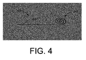
- FIG. 4 shows an example of a channel structure 400 that was milled using a focused ion beam.
- the sample includes an accumulation region 402 and a transport channel 404. While a spiral accumulation region is shown, any shape can be used.
- the accumulation region preferably includes channels that are sufficiently close together that the liquid in the adjacent channels will contact and join together.
- the channel allows the liquid to be delivered to a precise location, even though the location at which the nanocapillary contacts the substrate may not be precisely determined.
- Multiple channels can be used to cause small quantities of liquids to mix for performing nanochemistry reactions. That is, multiple nanodispersers can dispense small amounts of liquid to different points, and the liquid can follow the channels to a common working area, where the liquids mix together and react.
- the liquid transfers rapidly, for example, less than 10 seconds to move tens of microns.
- channels of length greater than 100 microns have been demonstrated. Some embodiments do not require an accumulation region.
- the transport channel itself may be where the fluid is desired to provide the liquid and where the processing occurs.
- the dimension across the top of the channel is preferably between 0.1 ⁇ m and 30 ⁇ m, more preferably between 0.1 ⁇ m and 10 ⁇ m, and more preferably between 0.1 ⁇ m and 5 ⁇ m.
- the channel depth is preferably between 0.1 ⁇ m and 20 ⁇ m, more preferably between 0.1 ⁇ m and 10 ⁇ m, and more preferably between 0.1 ⁇ m and 5 ⁇ m.
- the channel length is preferably between 0.1 ⁇ m and 500 ⁇ m, and more preferably between 0.1 um and 200 um.
- Channels may be straight or curved or contain segments meeting at an angle. Multiple channels may combine into fewer channels. Channels may branch out into a larger number of channels. Channels may optionally start, end, and/or traverse through larger fluid accumulation areas. Channels may pass alongside each other with a proximity designed to let the transported fluid either interact or not interact.
- FIG. 6 is a photomicrograph showing a nanocapillary 602 contacting the work piece surface along channel 404 and shows liquid 604 accumulated at accumulation point 402. In some embodiments there are multiple accumulation regions. In some embodiments, there are no accumulation regions, and the processing is performed on the fluid in the channels.
- processing may include, for example, directing a charged particle beam or laser beam at a region of the liquid.
- the liquid may be a precursor material that decomposes in the presence of a charged particle beam or laser beam to deposit material onto the work piece.
- the liquid may be a precursor material that reacts in the presence of a charged particle beam or laser beam to etch the work piece surface, forming volatile compounds that are removed from the vacuum chamber by a vacuum pump.
- the liquid may be a stain or a reactive liquid that reacts with material on the work piece.
- the liquid may be an electrolyte that is used to electrochemically deposit material onto the surface or to etch material from the surface, as described in Botman.
- FIG. 7 is a flowchart showing one method of preparing a nanocapillary for use with the present invention.
- the starting material can be, for example, a borosilicate tube having an inner diameter of 0.5 mm and having an internal filament to assist filling.
- Such nano-capillaries are commercially available from Sutter Instruments Company, Novato, CA.
- the nanocapillary is cleaned and baked.
- the nanocapillary is heated and pressure is applied along the long axis of the tube to create small tips, preferably less than 100 nm, at the end of the nanocapillary. This step is referred to as "pulling,” which can be performed using commercially available “pullers,” also available from Sutter Instruments Company.
- the nanocapillary tip is oriented for cutting the tip perpendicular to the long axis of the nanocapillary using a focused ion beam.
- the tip is cut.
- FIG. 9 shows the nanocapillary after being cut to expose an opening 902 in the end of nanocapillary 802.
- the nanocapillary is reoriented so that slits 1002 parallel to the long axis of the nanocapillary are cut in the tip.
- FIG. 10 shows the slits 1002.
- the slits in the tip facilitate liquid flow from the nanocapillary. While four slits 1002 are shown, fewer or more slits could be used. Moreover, the slits do not need to extend all the way through the nanocapillary tube - grooves in the nanocapillary interior could also be used. The slits provide a more reliable flow than prior art nanocapillaries.
- the nanocapillary After the nanocapillary is formed, it is filled in step 714.
- some embodiments of the invention use a nanocapillary having a sufficiently small inner diameter that the electrolyte flows by capillary action rather than by hydrostatic pressure.
- the small diameter of the nanocapillary makes filling difficult because of the surface tension of the liquid filling.
- Reliable and reproducible capillary flow when the nanocapillary touches the substrate within a vacuum chamber depends on the geometry of the tip of the nanocapillary and adequate filling of the nanocapillary with electrolyte.
- a method of filing a nanocapillary is described in Botman and also described below.
- the nanocapillary is attached to the micromanipulator.
- Good electrical contact between the conductive coating on the nanocapillary and the metal of the micromanipulator can be provided by applying silver paint to the junction. The drying of the silver takes about 10-20 minutes, and two layers are typically applied.
- the nanocapillary is then ready for use. It is positioned for dispensing liquid in step 718 and then contacted to the work piece surface in step 720.
- the flow from the nanocapillary to the substrate or surface is primarily due to capillary forces, and as such, the tip of the nanocapillary contacts the substrate directly to induce a flow.
- FIG. 11 describes a method for filling a nanocapillary.
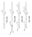
- FIG. 12 illustrates various steps of the process shown in FIG. 11 .
- FIG. 12 is adapted in part from FIG. 4 .3 from Donnermeyer, A. 2007. Thesis. Scanning Ion-Conductance Microscopy. Bielefeld (Germany): Bielefeld University .
- FIG. 12A shows a nanocapillary 1200, which includes an internal filament 1202 to facilitate filling.
- step 1102 illustrated by FIG. 12B , a fluid 1204 is placed inside the nanocapillary by filling it from the backside using a microloader 1206.
- the microloader is a syringe with a tip capable of fitting in the backside of the nanocapillary, where the diameter is about 500 microns or less.
- the internal filament in the nanocapillary causes some fluid 1204 to travel to the tip as shown by meniscus 1210 in FIG. 12C , much of the fluid remains away from the tip because of the small diameter of the nanocapillary 1200.
- the back end of the nanocapillary is sealed with vacuum compatible material 1208 to prevent the fluid inside the nanocapillary from evaporating into the vacuum from the back end of the nanocapillary.
- vacuum compatible wax is vacuum compatible wax.
- the wax used can be, for example, Apiezon Wax W. Mild heat (approximately 110°C) can be used to melt the wax and provide a good vacuum-tight seal. The fluid is thus effectively sealed inside the nanocapillary.
- a customized centrifuge uses a rotor from a 12 V computer fan, model FAN 3701 U from StarTech.
- the centrifuge is operated, for example, at 5000 rpm for 30 minutes, which is sufficient for reproducible and reliable filling of the nanocapillary tip with fluid.
- FIG. 12D shows the nanocapillary after step 1106 showing the additional fluid at the tip as shown by the movement of meniscus 1210.
- FIG. 14 shows two curves representing A and B from FIG. 13 .
- the evaporation rate depends on the temperature. As the temperature is increased, evaporation (B) increases. As the temperature is reduced, fluid can freeze (through evaporative cooling) at the nanocapillary tip, reducing the effective tip diameter. A reduced tip diameter reduces the amount of fluid that can flow out of the nanocapillary (A).
- Four regimes have been identified: (1) tip is almost fully blocked, very little flow; (2) tip is partially blocked, sub-maximal flow; (3) tip is fully unblocked, maximal flow; and (4) evaporation dominates; the user sees no bubble/drop.
- FIG. 15 represents the same information as FIG. 14 .
- the effective drop size in the 4 regimes described in FIG. 14 is plotted against temperature.
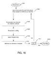
- FIG. 16 is a flowchart of occurrences during initial pumpdown of chamber from atmosphere to vacuum. Conditions can be such that the nanocapillary will be sealed by freezing of the liquid as the pressure is being reduced in the vacuum chamber. If sufficient time elapses (mere minutes), the system will end up in the "flow stops" state and the nanocapillary will effectively be sealed. This seal is good enough to keep the nanocapillary ready for use for many hours after the chamber is pumped down.
- the vacuum chamber begins to be evacuated, i.e. pumped down, to operating pressure.
- Block 1606 shows that the evaporation rate depends on chamber pressure and can be controlled by controlling the pumpdown.
- Block 1608 shows that the liquid is cooled as it evaporates and block 1610 shows that the liquid freezes at the tip, reducing the effective tip diameter in block 1612. If the tip is not fully blocked, then liquid continues to flow out of the tip in block 1604. If the tip is fully blocked in decision block 1614, the flow stops as shown in block 1616.
- the nanocapillary can remain in that state for several hours in preparation for further processing.
- FIG. 17 is a flowchart that describes how to reach an equilibrium between the work piece temperature and the evaporative cooling of the liquid after touchdown of the nanocapillary to the substrate.
- the equilibrium determines the effective tip diameter, which determines the fluid flow from the nanocapillary.
- FIG. 17 describes a method of controlling the flow of a liquid through a nanocapillary in a vacuum chamber by controlling the chamber pressure and/or the temperature of the liquid, the work piece, or both.
- the vacuum chamber pressure is typically less than 10 -4 mbar, more preferably less than 10 -5 mbar, and most preferably less than 10 -6 mbar.
- the vacuum chamber pressure typically varies between 0.1 mbar and 60 mbar, more preferably between 0.1 mbar and 20 mbar, and most preferably between 0.1 mbar and 10 mbar.
- the two states “flowing" and “non-flowing” are not final and given sufficient time or a change in conditions, can transition to the other state.
- the nanocapillary is placed in contact with the work piece in block 1702.
- decision block 1704 if the nanocapillary was not clogged, then liquid flows out of the nanocapillary and onto the work piece. As described in block 1706, the flow rate depends on the effective tip diameter.
- the liquid that has flowed out of nanocapillary evaporates, depending on the chamber pressure and the liquid temperature.
- Block 1710 shows evaporative cooling.
- Block 1712 indicates that the tip can be considered, in a short time frame, a thermally closed system so it cools down and some of the liquid freezes at the tip in block 1712, effectively reducing the tip diameter in block 1714.
- decision block 1716 if the tip is fully blocked, there is no flow as shown in block 1730. If not, the liquid flow continues in block 1718 and can achieve an equilibrium flow rate. If it is desired to increase the flow rate, the temperature of the work piece may be raised in block 1722 until a new long-term equilibrium is reached in block 1720, and liquid continues to flow in block 1706.
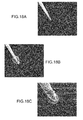
- FIG. 18A shows the nanocapillary before it contacts the work piece.
- FIG 18B shows the nanocapillary after touchdown with a small drop when the chamber is still in high vacuum mode.
- FIG. 18C shows the drop after a period of time and shows that drops can have a diameter as small as 4 microns.
- the liquid can form a bubble having a diameter of preferably less than 30 ⁇ m, more preferably less than 10 ⁇ m, and most preferably less than 2 ⁇ m.
- FIG. 19 shows another capillary 1900 that can also be used in some embodiments of the invention.
- the nanocapillary of FIG. 19 does not include slits near the tip. It includes an angled tip 1902 and an alignment mark 1904, as described in Botman.
- FIG. 20 shows a system in which a nanocapillary is used to dispense an electrolyte for electrochemical deposition or etching.
- an embodiment suitable for use within a charged particle beam vacuum chamber allows steps that require charged particle beam processing and steps that require electrochemical processing to be performed without repeatedly moving the work piece into and out of a vacuum chamber. Such embodiments eliminate the time consuming step of pumping down the vacuum chamber to an adequate vacuum between process steps. Also, maintaining the work piece within a vacuum chamber reduces contamination.
- nanocapillary shown in FIG. 19 and described by Botman can be used in embodiments of the invention, as well as the nanocapillary shown in FIG. 10 .
- FIG. 2 describes the use of the invention with a beam-induced process.
- FIG. 20 shows the use of the invention for electrochemical deposition or etching.
- FIG. 20 shows an embodiment of the invention in which a nanocapillary 2002 is used for electrochemical deposition or etching within sample vacuum chamber 2004 of a charged particle beam system 2006, such as an environmental scanning electron microscope.
- Nanocapillary 2002 is used to deliver electrolyte solution 2008 to a surface 2010.
- a channel 2009 connects the location at which nanocapillary 2002 contacts the surface 2010 to an accumulation point that corresponds to the processing location 2011.
- the electrolyte flows through the channel and forms a bubble 2014 at the accumulation point, as described with respect to FIGS. 4 and 6 .
- the nanocapillary of FIG. 10 is used to deliver the electrolyte, using the method of FIG. 17 to control the fluid flow.
- Nanocapillary 2002 is attached to a micromanipulator 2012 that preferably provides motion in three axes and rotation along the capillary axis.
- a modified gas injection system which is a common accessory in charged particle beam systems, can be used as the micromanipulator.
- One electrode for electrochemical deposition is provided by a conductive coating 2018 on, or a wire (not shown) in or on, nanocapillary 2002.
- the electrode associated with the nanocapillary is positively biased.
- surface 2010 is conductive and is connected through the sample substrate 2020 or through a surface probe (not shown) to an electrode 2024 to provide a second contact for electrochemical processing.
- the charged particle beam can function as a virtual cathode or anode, providing charges for the electrochemical reaction.
- the electrochemical deposition or etching can be observed by the environmental scanning electron microscopy 2006, in which electron beam 2031 scans the region where material is being deposited and secondary electrons 2034 are emitted upon impact of electron beam 2031.
- the secondary electrons 2034 are amplified by gas cascade amplification and detected by an electrode 2040, forming an image whose brightness at each point corresponds to the current detected by the electrode 2040.
- the image can be used to monitor and adjust the progress of the electrochemical deposition or etching to provide real time feedback to an operator.
- the image can be used to position and guide the nanocapillary 2002 during deposition or etch.
- the diameter of the nanodispenser is preferably sufficiently small so that the electrolyte is forced out of the nanocapillary by capillary action when the capillary is in contact with the surface, rather than through hydrostatic pressure.
- a method of processing a work piece in a vacuum chamber comprises dispensing a liquid onto the work piece; and directing a charged particle beam to the work piece; characterized by forming a channel on the surface of the work piece in the vacuum chamber; dispensing the liquid onto the work piece comprises dispensing the liquid into the channel at a first position, the liquid flowing through the channel to a second position on the work piece; and directing the charged particle beam to the work piece comprises directing the charged particle beam to the second position on the work piece, the charged particle beam reacting with the liquid at the second position to form a structure on the work piece.
- forming the channel on the surface comprises directing a beam of ions or a photon beam toward the substrate to remove material to form the channel.
- dispensing a liquid into the channel includes dispensing a deposition precursor, an etch precursor, or an electrolyte.
- forming a structure on the work piece comprises directing a charged particle beam or a laser beam toward the second position, the charged particle beam initiating a reaction of the liquid to deposit or etch material from the surface. In some embodiments, forming a structure on the work piece comprises passing an electric current through the liquid to electrochemically deposit material onto the surface or to electrochemically remove material from the surface.
- the method further comprises providing a cover over a portion of the channel between the first position and the second position to reduce evaporation of the liquid.
- dispensing a liquid comprises providing a nanocapillary having a diameter at the tip of less than 50 ⁇ m and having at least one slit cut into the nanocapillary, the slit(s) extending to the tip; and contacting the tip of the nanocapillary to the work piece surface to dispense liquid from the nanocapillary onto the work piece.
- contacting the tip of the nanocapillary to the work piece surface to dispense liquid from the nanocapillary onto the work piece comprises contacting the tip of the nanocapillary to the work piece surface to dispense liquid from the nanocapillary onto the work piece using primarily capillary forces.
- contacting the tip of the nanocapillary to the work piece surface to dispense liquid from the nanocapillary onto the work piece comprises dispensing a drop of liquid having a diameter of less than 50 ⁇ m onto the surface. In some embodiments, dispensing a drop of liquid having a diameter of less than 50 ⁇ m to the surface comprises dispensing a drop of liquid having a diameter of less than 10 ⁇ m.
- dispensing a liquid comprises controlling the flow of liquid from a nanocapillary by contacting the nanodispenser to the work piece surface in the vacuum chamber to form a bubble of liquid at the tip of the dispenser; adjusting the pressure in the vacuum chamber to control the rate of evaporation of the bubble; and adjusting the temperature of the liquid to control the rate of flow into the bubble, the equilibrium between the evaporation and the flow rate of liquid into the bubble determining the bubble size.
- adjusting the temperature of the liquid comprises adjusting the temperature of the nanodispenser or the temperature of the work piece. In some embodiments, adjusting the temperature of the liquid comprises controlling the amount of frozen liquid at the tip by adjusting the size of the opening at the tip of the nanodispenser.
- a liquid nanodispenser comprises a hollow tube for containing a liquid, the hollow tube having an inner diameter of less than 50 microns at the tip, characterized in that the tip includes slits that extend to the tube opening for facilitating fluid flow by capillary action from the interior of the tube to a contacted work piece surface.
- the hollow tube is coated with a conductive material.
- the invention has multiple aspects that are separately patentable and not all aspects will be used in all embodiments.
Landscapes
- Chemical & Material Sciences (AREA)
- Physics & Mathematics (AREA)
- Health & Medical Sciences (AREA)
- Life Sciences & Earth Sciences (AREA)
- Analytical Chemistry (AREA)
- Biochemistry (AREA)
- General Health & Medical Sciences (AREA)
- General Physics & Mathematics (AREA)
- Immunology (AREA)
- Pathology (AREA)
- Materials Engineering (AREA)
- Engineering & Computer Science (AREA)
- Chemical Kinetics & Catalysis (AREA)
- Electrochemistry (AREA)
- Metallurgy (AREA)
- Organic Chemistry (AREA)
- Optics & Photonics (AREA)
- Electromagnetism (AREA)
- Micromachines (AREA)
- Welding Or Cutting Using Electron Beams (AREA)
- Carbon And Carbon Compounds (AREA)
- Sampling And Sample Adjustment (AREA)
Applications Claiming Priority (1)
| Application Number | Priority Date | Filing Date | Title |
|---|---|---|---|
| US13/693,938 US9044781B2 (en) | 2012-12-04 | 2012-12-04 | Microfluidics delivery systems |
Publications (3)
| Publication Number | Publication Date |
|---|---|
| EP2741075A2 true EP2741075A2 (de) | 2014-06-11 |
| EP2741075A3 EP2741075A3 (de) | 2015-01-07 |
| EP2741075B1 EP2741075B1 (de) | 2016-05-04 |
Family
ID=49989412
Family Applications (1)
| Application Number | Title | Priority Date | Filing Date |
|---|---|---|---|
| EP13195225.1A Active EP2741075B1 (de) | 2012-12-04 | 2013-12-02 | Verfahren zur Verarbeitung eines Werkstückes in einer Vakuumkammer |
Country Status (4)
| Country | Link |
|---|---|
| US (1) | US9044781B2 (de) |
| EP (1) | EP2741075B1 (de) |
| JP (1) | JP6411022B2 (de) |
| CN (1) | CN103855083B (de) |
Cited By (2)
| Publication number | Priority date | Publication date | Assignee | Title |
|---|---|---|---|---|
| EP3043372A1 (de) * | 2015-01-12 | 2016-07-13 | Fei Company | Verfahren zur Modifizierung einer Probenoberflächenschicht aus einer mikroskopischen Probe |
| WO2019179794A1 (en) * | 2018-03-23 | 2019-09-26 | Uniwersytet Jagiellonski | Conducting a reaction in a meniscus moved over a substrate |
Families Citing this family (6)
| Publication number | Priority date | Publication date | Assignee | Title |
|---|---|---|---|---|
| US8872105B2 (en) * | 2013-02-19 | 2014-10-28 | Fei Company | In situ reactivation of fluorescence marker |
| CN104099239B (zh) * | 2014-07-10 | 2016-04-20 | 中国农业科学院北京畜牧兽医研究所 | 一种显微操作持定针的制作方法 |
| KR102086740B1 (ko) | 2017-10-20 | 2020-03-09 | 서강대학교산학협력단 | 모세관을 이용한 나노입자 단일층의 전이 방법 및 장치 |
| WO2019078676A2 (ko) * | 2017-10-20 | 2019-04-25 | 서강대학교산학협력단 | 모세관을 이용한 나노입자 단일층의 전이 방법 및 장치 |
| CN110315464B (zh) * | 2019-08-06 | 2020-09-29 | 哈尔滨理工大学 | 一种基于电化学沉积的金属微构件拾取方法 |
| KR102619877B1 (ko) | 2019-09-11 | 2024-01-03 | 삼성전자주식회사 | 기판 처리 장치 |
Citations (4)
| Publication number | Priority date | Publication date | Assignee | Title |
|---|---|---|---|---|
| US4876112A (en) | 1986-05-29 | 1989-10-24 | Seiko Instruments Inc. | Process for forming metallic patterned film |
| US5104684A (en) | 1990-05-25 | 1992-04-14 | Massachusetts Institute Of Technology | Ion beam induced deposition of metals |
| US7674706B2 (en) | 2004-04-13 | 2010-03-09 | Fei Company | System for modifying small structures using localized charge transfer mechanism to remove or deposit material |
| US7977631B2 (en) | 2006-08-16 | 2011-07-12 | Fei Company | Method for obtaining images from slices of specimen |
Family Cites Families (15)
| Publication number | Priority date | Publication date | Assignee | Title |
|---|---|---|---|---|
| US5051237A (en) * | 1988-06-23 | 1991-09-24 | P B Diagnostic Systems, Inc. | Liquid transport system |
| US6348295B1 (en) | 1999-03-26 | 2002-02-19 | Massachusetts Institute Of Technology | Methods for manufacturing electronic and electromechanical elements and devices by thin-film deposition and imaging |
| DE10017825C2 (de) | 2000-04-10 | 2003-05-08 | Till I D Gmbh | Polychromatische Fluoreszenz-Meßvorrichtung |
| WO2003031044A2 (en) * | 2001-10-05 | 2003-04-17 | Vanderbilt University | Capillary tube printing tips for microarray printing |
| US7250139B2 (en) | 2003-03-19 | 2007-07-31 | Northwestern University | Nanotipped device and method |
| US20040265171A1 (en) * | 2003-06-27 | 2004-12-30 | Pugia Michael J. | Method for uniform application of fluid into a reactive reagent area |
| US7893386B2 (en) * | 2003-11-14 | 2011-02-22 | Hewlett-Packard Development Company, L.P. | Laser micromachining and methods of same |
| WO2006004929A2 (en) * | 2004-06-28 | 2006-01-12 | Boise State University | Electrochemical deposition method utilizing microdroplets of solution |
| NL1027462C2 (nl) * | 2004-11-09 | 2006-05-10 | Koninkl Philips Electronics Nv | Werkwijze voor het lokaliseren van fluorescente markers. |
| US7740806B2 (en) * | 2006-02-28 | 2010-06-22 | International Business Machines Corporation | Ceramic microarray spotting device for bioassay printing |
| CN103201609A (zh) | 2010-09-21 | 2013-07-10 | Fei公司 | 制备供电子显微镜和荧光显微镜观察的生物样品的方法 |
| US8319181B2 (en) | 2011-01-30 | 2012-11-27 | Fei Company | System and method for localization of large numbers of fluorescent markers in biological samples |
| US8853078B2 (en) | 2011-01-30 | 2014-10-07 | Fei Company | Method of depositing material |
| US9583354B2 (en) | 2011-03-30 | 2017-02-28 | The Aerospace Corporation | Systems and methods for depositing materials on either side of a freestanding film using laser-assisted chemical vapor deposition (LA-CVD), and structures formed using same |
| US9255339B2 (en) * | 2011-09-19 | 2016-02-09 | Fei Company | Localized, in-vacuum modification of small structures |
-
2012
- 2012-12-04 US US13/693,938 patent/US9044781B2/en active Active
-
2013
- 2013-11-20 JP JP2013240123A patent/JP6411022B2/ja active Active
- 2013-12-02 EP EP13195225.1A patent/EP2741075B1/de active Active
- 2013-12-03 CN CN201310641651.4A patent/CN103855083B/zh active Active
Patent Citations (4)
| Publication number | Priority date | Publication date | Assignee | Title |
|---|---|---|---|---|
| US4876112A (en) | 1986-05-29 | 1989-10-24 | Seiko Instruments Inc. | Process for forming metallic patterned film |
| US5104684A (en) | 1990-05-25 | 1992-04-14 | Massachusetts Institute Of Technology | Ion beam induced deposition of metals |
| US7674706B2 (en) | 2004-04-13 | 2010-03-09 | Fei Company | System for modifying small structures using localized charge transfer mechanism to remove or deposit material |
| US7977631B2 (en) | 2006-08-16 | 2011-07-12 | Fei Company | Method for obtaining images from slices of specimen |
Non-Patent Citations (2)
| Title |
|---|
| DONNERMEYER, A.: "Scanning lon-Conductance Microscopy", THESIS, 2007 |
| SURYAVANSHI ET AL.: "Probe-based electrochemical fabrication of freestanding Cu nanowire array", APPLIED PHYSICS LETTERS, vol. 88, 2006, pages 083103 |
Cited By (3)
| Publication number | Priority date | Publication date | Assignee | Title |
|---|---|---|---|---|
| EP3043372A1 (de) * | 2015-01-12 | 2016-07-13 | Fei Company | Verfahren zur Modifizierung einer Probenoberflächenschicht aus einer mikroskopischen Probe |
| US10105734B2 (en) | 2015-01-12 | 2018-10-23 | Fei Company | Method of modifying a sample surface layer from a microscopic sample |
| WO2019179794A1 (en) * | 2018-03-23 | 2019-09-26 | Uniwersytet Jagiellonski | Conducting a reaction in a meniscus moved over a substrate |
Also Published As
| Publication number | Publication date |
|---|---|
| US20140151335A1 (en) | 2014-06-05 |
| US9044781B2 (en) | 2015-06-02 |
| JP2014128871A (ja) | 2014-07-10 |
| CN103855083B (zh) | 2019-07-16 |
| JP6411022B2 (ja) | 2018-10-24 |
| EP2741075B1 (de) | 2016-05-04 |
| CN103855083A (zh) | 2014-06-11 |
| EP2741075A3 (de) | 2015-01-07 |
Similar Documents
| Publication | Publication Date | Title |
|---|---|---|
| EP2741075B1 (de) | Verfahren zur Verarbeitung eines Werkstückes in einer Vakuumkammer | |
| US9812286B2 (en) | Localized, in-vacuum modification of small structures | |
| US12059698B2 (en) | Systems and methods of electron beam induced processing | |
| US8709269B2 (en) | Method and system for imaging a cross section of a specimen | |
| US7531797B2 (en) | Probe-holding apparatus, sample-obtaining apparatus, sample-processing apparatus, sample-processing method and sample-evaluating method | |
| EP2749863A2 (de) | Verfahren zur Vorbereitung von Proben für Bildgebung | |
| CN110565130A (zh) | 一种激光增强三维微区电沉积方法及其对应的装置 | |
| US9263306B2 (en) | Protective layer for charged particle beam processing | |
| JP6110519B2 (ja) | 顕微鏡サンプルからサンプル表面層を改変する方法 | |
| Xu et al. | Etching of glass, silicon, and silicon dioxide using negative ionic liquid ion sources | |
| JP2009037910A (ja) | 複合荷電粒子ビーム装置及び加工観察方法 | |
| JP2016130733A5 (de) | ||
| Miller et al. | The art of specimen preparation | |
| Bachmann | Focused ion beam micro-machining | |
| EP3502654A1 (de) | Verfahren zum aufbringen von flüssigkeiten auf ein substrat | |
| Li et al. | Pure and conformal CVD nickel and nickel monosilicide in high-aspect-ratio structures analyzed by atom probe tomography | |
| US12176177B2 (en) | Ion beam chamber fluid delivery apparatus and method and ion beam etcher using same | |
| Li | Direct Liquid Evaporation Chemical Vapor Deposition (DLE-CVD) of Nickel, Manganese and Copper-Based Thin Films for Interconnects in Three-Dimensional Microelectronic Systems | |
| JP2011062666A (ja) | 成膜装置、その成膜装置を用いた振動子、及び成膜方法 |
Legal Events
| Date | Code | Title | Description |
|---|---|---|---|
| PUAI | Public reference made under article 153(3) epc to a published international application that has entered the european phase |
Free format text: ORIGINAL CODE: 0009012 |
|
| 17P | Request for examination filed |
Effective date: 20131202 |
|
| AK | Designated contracting states |
Kind code of ref document: A2 Designated state(s): AL AT BE BG CH CY CZ DE DK EE ES FI FR GB GR HR HU IE IS IT LI LT LU LV MC MK MT NL NO PL PT RO RS SE SI SK SM TR |
|
| AX | Request for extension of the european patent |
Extension state: BA ME |
|
| RIC1 | Information provided on ipc code assigned before grant |
Ipc: G01N 23/225 20060101AFI20140922BHEP |
|
| PUAL | Search report despatched |
Free format text: ORIGINAL CODE: 0009013 |
|
| AK | Designated contracting states |
Kind code of ref document: A3 Designated state(s): AL AT BE BG CH CY CZ DE DK EE ES FI FR GB GR HR HU IE IS IT LI LT LU LV MC MK MT NL NO PL PT RO RS SE SI SK SM TR |
|
| AX | Request for extension of the european patent |
Extension state: BA ME |
|
| RIC1 | Information provided on ipc code assigned before grant |
Ipc: G01N 23/225 20060101AFI20141204BHEP |
|
| R17P | Request for examination filed (corrected) |
Effective date: 20150617 |
|
| RBV | Designated contracting states (corrected) |
Designated state(s): AL AT BE BG CH CY CZ DE DK EE ES FI FR GB GR HR HU IE IS IT LI LT LU LV MC MK MT NL NO PL PT RO RS SE SI SK SM TR |
|
| GRAP | Despatch of communication of intention to grant a patent |
Free format text: ORIGINAL CODE: EPIDOSNIGR1 |
|
| INTG | Intention to grant announced |
Effective date: 20160118 |
|
| GRAS | Grant fee paid |
Free format text: ORIGINAL CODE: EPIDOSNIGR3 |
|
| GRAA | (expected) grant |
Free format text: ORIGINAL CODE: 0009210 |
|
| AK | Designated contracting states |
Kind code of ref document: B1 Designated state(s): AL AT BE BG CH CY CZ DE DK EE ES FI FR GB GR HR HU IE IS IT LI LT LU LV MC MK MT NL NO PL PT RO RS SE SI SK SM TR |
|
| REG | Reference to a national code |
Ref country code: GB Ref legal event code: FG4D |
|
| REG | Reference to a national code |
Ref country code: CH Ref legal event code: EP |
|
| REG | Reference to a national code |
Ref country code: AT Ref legal event code: REF Ref document number: 797357 Country of ref document: AT Kind code of ref document: T Effective date: 20160515 |
|
| REG | Reference to a national code |
Ref country code: IE Ref legal event code: FG4D |
|
| REG | Reference to a national code |
Ref country code: DE Ref legal event code: R096 Ref document number: 602013007236 Country of ref document: DE |
|
| REG | Reference to a national code |
Ref country code: NL Ref legal event code: MP Effective date: 20160504 |
|
| REG | Reference to a national code |
Ref country code: LT Ref legal event code: MG4D |
|
| PG25 | Lapsed in a contracting state [announced via postgrant information from national office to epo] |
Ref country code: NL Free format text: LAPSE BECAUSE OF FAILURE TO SUBMIT A TRANSLATION OF THE DESCRIPTION OR TO PAY THE FEE WITHIN THE PRESCRIBED TIME-LIMIT Effective date: 20160504 Ref country code: FI Free format text: LAPSE BECAUSE OF FAILURE TO SUBMIT A TRANSLATION OF THE DESCRIPTION OR TO PAY THE FEE WITHIN THE PRESCRIBED TIME-LIMIT Effective date: 20160504 Ref country code: LT Free format text: LAPSE BECAUSE OF FAILURE TO SUBMIT A TRANSLATION OF THE DESCRIPTION OR TO PAY THE FEE WITHIN THE PRESCRIBED TIME-LIMIT Effective date: 20160504 Ref country code: NO Free format text: LAPSE BECAUSE OF FAILURE TO SUBMIT A TRANSLATION OF THE DESCRIPTION OR TO PAY THE FEE WITHIN THE PRESCRIBED TIME-LIMIT Effective date: 20160804 |
|
| REG | Reference to a national code |
Ref country code: AT Ref legal event code: MK05 Ref document number: 797357 Country of ref document: AT Kind code of ref document: T Effective date: 20160504 |
|
| PG25 | Lapsed in a contracting state [announced via postgrant information from national office to epo] |
Ref country code: GR Free format text: LAPSE BECAUSE OF FAILURE TO SUBMIT A TRANSLATION OF THE DESCRIPTION OR TO PAY THE FEE WITHIN THE PRESCRIBED TIME-LIMIT Effective date: 20160805 Ref country code: RS Free format text: LAPSE BECAUSE OF FAILURE TO SUBMIT A TRANSLATION OF THE DESCRIPTION OR TO PAY THE FEE WITHIN THE PRESCRIBED TIME-LIMIT Effective date: 20160504 Ref country code: LV Free format text: LAPSE BECAUSE OF FAILURE TO SUBMIT A TRANSLATION OF THE DESCRIPTION OR TO PAY THE FEE WITHIN THE PRESCRIBED TIME-LIMIT Effective date: 20160504 Ref country code: HR Free format text: LAPSE BECAUSE OF FAILURE TO SUBMIT A TRANSLATION OF THE DESCRIPTION OR TO PAY THE FEE WITHIN THE PRESCRIBED TIME-LIMIT Effective date: 20160504 Ref country code: ES Free format text: LAPSE BECAUSE OF FAILURE TO SUBMIT A TRANSLATION OF THE DESCRIPTION OR TO PAY THE FEE WITHIN THE PRESCRIBED TIME-LIMIT Effective date: 20160504 Ref country code: PT Free format text: LAPSE BECAUSE OF FAILURE TO SUBMIT A TRANSLATION OF THE DESCRIPTION OR TO PAY THE FEE WITHIN THE PRESCRIBED TIME-LIMIT Effective date: 20160905 Ref country code: SE Free format text: LAPSE BECAUSE OF FAILURE TO SUBMIT A TRANSLATION OF THE DESCRIPTION OR TO PAY THE FEE WITHIN THE PRESCRIBED TIME-LIMIT Effective date: 20160504 |
|
| REG | Reference to a national code |
Ref country code: FR Ref legal event code: PLFP Year of fee payment: 4 |
|
| PG25 | Lapsed in a contracting state [announced via postgrant information from national office to epo] |
Ref country code: IT Free format text: LAPSE BECAUSE OF FAILURE TO SUBMIT A TRANSLATION OF THE DESCRIPTION OR TO PAY THE FEE WITHIN THE PRESCRIBED TIME-LIMIT Effective date: 20160504 |
|
| PG25 | Lapsed in a contracting state [announced via postgrant information from national office to epo] |
Ref country code: CZ Free format text: LAPSE BECAUSE OF FAILURE TO SUBMIT A TRANSLATION OF THE DESCRIPTION OR TO PAY THE FEE WITHIN THE PRESCRIBED TIME-LIMIT Effective date: 20160504 Ref country code: EE Free format text: LAPSE BECAUSE OF FAILURE TO SUBMIT A TRANSLATION OF THE DESCRIPTION OR TO PAY THE FEE WITHIN THE PRESCRIBED TIME-LIMIT Effective date: 20160504 Ref country code: RO Free format text: LAPSE BECAUSE OF FAILURE TO SUBMIT A TRANSLATION OF THE DESCRIPTION OR TO PAY THE FEE WITHIN THE PRESCRIBED TIME-LIMIT Effective date: 20160504 Ref country code: SK Free format text: LAPSE BECAUSE OF FAILURE TO SUBMIT A TRANSLATION OF THE DESCRIPTION OR TO PAY THE FEE WITHIN THE PRESCRIBED TIME-LIMIT Effective date: 20160504 Ref country code: DK Free format text: LAPSE BECAUSE OF FAILURE TO SUBMIT A TRANSLATION OF THE DESCRIPTION OR TO PAY THE FEE WITHIN THE PRESCRIBED TIME-LIMIT Effective date: 20160504 |
|
| REG | Reference to a national code |
Ref country code: DE Ref legal event code: R097 Ref document number: 602013007236 Country of ref document: DE |
|
| PG25 | Lapsed in a contracting state [announced via postgrant information from national office to epo] |
Ref country code: BE Free format text: LAPSE BECAUSE OF FAILURE TO SUBMIT A TRANSLATION OF THE DESCRIPTION OR TO PAY THE FEE WITHIN THE PRESCRIBED TIME-LIMIT Effective date: 20160504 Ref country code: AT Free format text: LAPSE BECAUSE OF FAILURE TO SUBMIT A TRANSLATION OF THE DESCRIPTION OR TO PAY THE FEE WITHIN THE PRESCRIBED TIME-LIMIT Effective date: 20160504 Ref country code: PL Free format text: LAPSE BECAUSE OF FAILURE TO SUBMIT A TRANSLATION OF THE DESCRIPTION OR TO PAY THE FEE WITHIN THE PRESCRIBED TIME-LIMIT Effective date: 20160504 Ref country code: SM Free format text: LAPSE BECAUSE OF FAILURE TO SUBMIT A TRANSLATION OF THE DESCRIPTION OR TO PAY THE FEE WITHIN THE PRESCRIBED TIME-LIMIT Effective date: 20160504 |
|
| PLBE | No opposition filed within time limit |
Free format text: ORIGINAL CODE: 0009261 |
|
| STAA | Information on the status of an ep patent application or granted ep patent |
Free format text: STATUS: NO OPPOSITION FILED WITHIN TIME LIMIT |
|
| 26N | No opposition filed |
Effective date: 20170207 |
|
| PG25 | Lapsed in a contracting state [announced via postgrant information from national office to epo] |
Ref country code: SI Free format text: LAPSE BECAUSE OF FAILURE TO SUBMIT A TRANSLATION OF THE DESCRIPTION OR TO PAY THE FEE WITHIN THE PRESCRIBED TIME-LIMIT Effective date: 20160504 |
|
| PG25 | Lapsed in a contracting state [announced via postgrant information from national office to epo] |
Ref country code: MC Free format text: LAPSE BECAUSE OF FAILURE TO SUBMIT A TRANSLATION OF THE DESCRIPTION OR TO PAY THE FEE WITHIN THE PRESCRIBED TIME-LIMIT Effective date: 20160504 |
|
| REG | Reference to a national code |
Ref country code: CH Ref legal event code: PL |
|
| REG | Reference to a national code |
Ref country code: IE Ref legal event code: MM4A |
|
| PG25 | Lapsed in a contracting state [announced via postgrant information from national office to epo] |
Ref country code: CH Free format text: LAPSE BECAUSE OF NON-PAYMENT OF DUE FEES Effective date: 20161231 Ref country code: LU Free format text: LAPSE BECAUSE OF NON-PAYMENT OF DUE FEES Effective date: 20161202 Ref country code: LI Free format text: LAPSE BECAUSE OF NON-PAYMENT OF DUE FEES Effective date: 20161231 |
|
| REG | Reference to a national code |
Ref country code: FR Ref legal event code: PLFP Year of fee payment: 5 |
|
| PG25 | Lapsed in a contracting state [announced via postgrant information from national office to epo] |
Ref country code: IE Free format text: LAPSE BECAUSE OF NON-PAYMENT OF DUE FEES Effective date: 20161202 |
|
| PG25 | Lapsed in a contracting state [announced via postgrant information from national office to epo] |
Ref country code: HU Free format text: LAPSE BECAUSE OF FAILURE TO SUBMIT A TRANSLATION OF THE DESCRIPTION OR TO PAY THE FEE WITHIN THE PRESCRIBED TIME-LIMIT; INVALID AB INITIO Effective date: 20131202 |
|
| PG25 | Lapsed in a contracting state [announced via postgrant information from national office to epo] |
Ref country code: CY Free format text: LAPSE BECAUSE OF FAILURE TO SUBMIT A TRANSLATION OF THE DESCRIPTION OR TO PAY THE FEE WITHIN THE PRESCRIBED TIME-LIMIT Effective date: 20160504 Ref country code: MK Free format text: LAPSE BECAUSE OF FAILURE TO SUBMIT A TRANSLATION OF THE DESCRIPTION OR TO PAY THE FEE WITHIN THE PRESCRIBED TIME-LIMIT Effective date: 20160504 Ref country code: IS Free format text: LAPSE BECAUSE OF FAILURE TO SUBMIT A TRANSLATION OF THE DESCRIPTION OR TO PAY THE FEE WITHIN THE PRESCRIBED TIME-LIMIT Effective date: 20160504 |
|
| PG25 | Lapsed in a contracting state [announced via postgrant information from national office to epo] |
Ref country code: BG Free format text: LAPSE BECAUSE OF FAILURE TO SUBMIT A TRANSLATION OF THE DESCRIPTION OR TO PAY THE FEE WITHIN THE PRESCRIBED TIME-LIMIT Effective date: 20160504 |
|
| PG25 | Lapsed in a contracting state [announced via postgrant information from national office to epo] |
Ref country code: MT Free format text: LAPSE BECAUSE OF NON-PAYMENT OF DUE FEES Effective date: 20161202 |
|
| PG25 | Lapsed in a contracting state [announced via postgrant information from national office to epo] |
Ref country code: TR Free format text: LAPSE BECAUSE OF FAILURE TO SUBMIT A TRANSLATION OF THE DESCRIPTION OR TO PAY THE FEE WITHIN THE PRESCRIBED TIME-LIMIT Effective date: 20160504 Ref country code: AL Free format text: LAPSE BECAUSE OF FAILURE TO SUBMIT A TRANSLATION OF THE DESCRIPTION OR TO PAY THE FEE WITHIN THE PRESCRIBED TIME-LIMIT Effective date: 20160504 |
|
| P01 | Opt-out of the competence of the unified patent court (upc) registered |
Effective date: 20230520 |
|
| PGFP | Annual fee paid to national office [announced via postgrant information from national office to epo] |
Ref country code: DE Payment date: 20251113 Year of fee payment: 13 |
|
| PGFP | Annual fee paid to national office [announced via postgrant information from national office to epo] |
Ref country code: GB Payment date: 20251208 Year of fee payment: 13 |
|
| PGFP | Annual fee paid to national office [announced via postgrant information from national office to epo] |
Ref country code: FR Payment date: 20251212 Year of fee payment: 13 |