EP2738888A2 - Light emitting device and vehicle lamp - Google Patents
Light emitting device and vehicle lamp Download PDFInfo
- Publication number
- EP2738888A2 EP2738888A2 EP13020131.2A EP13020131A EP2738888A2 EP 2738888 A2 EP2738888 A2 EP 2738888A2 EP 13020131 A EP13020131 A EP 13020131A EP 2738888 A2 EP2738888 A2 EP 2738888A2
- Authority
- EP
- European Patent Office
- Prior art keywords
- light
- transmitting member
- light emitting
- hole
- emitting device
- Prior art date
- Legal status (The legal status is an assumption and is not a legal conclusion. Google has not performed a legal analysis and makes no representation as to the accuracy of the status listed.)
- Withdrawn
Links
Images






Classifications
-
- F—MECHANICAL ENGINEERING; LIGHTING; HEATING; WEAPONS; BLASTING
- F21—LIGHTING
- F21S—NON-PORTABLE LIGHTING DEVICES; SYSTEMS THEREOF; VEHICLE LIGHTING DEVICES SPECIALLY ADAPTED FOR VEHICLE EXTERIORS
- F21S41/00—Illuminating devices specially adapted for vehicle exteriors, e.g. headlamps
- F21S41/10—Illuminating devices specially adapted for vehicle exteriors, e.g. headlamps characterised by the light source
- F21S41/14—Illuminating devices specially adapted for vehicle exteriors, e.g. headlamps characterised by the light source characterised by the type of light source
- F21S41/16—Laser light sources
-
- F—MECHANICAL ENGINEERING; LIGHTING; HEATING; WEAPONS; BLASTING
- F21—LIGHTING
- F21K—NON-ELECTRIC LIGHT SOURCES USING LUMINESCENCE; LIGHT SOURCES USING ELECTROCHEMILUMINESCENCE; LIGHT SOURCES USING CHARGES OF COMBUSTIBLE MATERIAL; LIGHT SOURCES USING SEMICONDUCTOR DEVICES AS LIGHT-GENERATING ELEMENTS; LIGHT SOURCES NOT OTHERWISE PROVIDED FOR
- F21K9/00—Light sources using semiconductor devices as light-generating elements, e.g. using light-emitting diodes [LED] or lasers
- F21K9/60—Optical arrangements integrated in the light source, e.g. for improving the colour rendering index or the light extraction
-
- F—MECHANICAL ENGINEERING; LIGHTING; HEATING; WEAPONS; BLASTING
- F21—LIGHTING
- F21S—NON-PORTABLE LIGHTING DEVICES; SYSTEMS THEREOF; VEHICLE LIGHTING DEVICES SPECIALLY ADAPTED FOR VEHICLE EXTERIORS
- F21S41/00—Illuminating devices specially adapted for vehicle exteriors, e.g. headlamps
- F21S41/10—Illuminating devices specially adapted for vehicle exteriors, e.g. headlamps characterised by the light source
- F21S41/14—Illuminating devices specially adapted for vehicle exteriors, e.g. headlamps characterised by the light source characterised by the type of light source
- F21S41/141—Light emitting diodes [LED]
- F21S41/143—Light emitting diodes [LED] the main emission direction of the LED being parallel to the optical axis of the illuminating device
-
- F—MECHANICAL ENGINEERING; LIGHTING; HEATING; WEAPONS; BLASTING
- F21—LIGHTING
- F21S—NON-PORTABLE LIGHTING DEVICES; SYSTEMS THEREOF; VEHICLE LIGHTING DEVICES SPECIALLY ADAPTED FOR VEHICLE EXTERIORS
- F21S41/00—Illuminating devices specially adapted for vehicle exteriors, e.g. headlamps
- F21S41/10—Illuminating devices specially adapted for vehicle exteriors, e.g. headlamps characterised by the light source
- F21S41/14—Illuminating devices specially adapted for vehicle exteriors, e.g. headlamps characterised by the light source characterised by the type of light source
- F21S41/176—Light sources where the light is generated by photoluminescent material spaced from a primary light generating element
-
- F—MECHANICAL ENGINEERING; LIGHTING; HEATING; WEAPONS; BLASTING
- F21—LIGHTING
- F21S—NON-PORTABLE LIGHTING DEVICES; SYSTEMS THEREOF; VEHICLE LIGHTING DEVICES SPECIALLY ADAPTED FOR VEHICLE EXTERIORS
- F21S41/00—Illuminating devices specially adapted for vehicle exteriors, e.g. headlamps
- F21S41/20—Illuminating devices specially adapted for vehicle exteriors, e.g. headlamps characterised by refractors, transparent cover plates, light guides or filters
- F21S41/285—Refractors, transparent cover plates, light guides or filters not provided in groups F21S41/24 - F21S41/2805
-
- F—MECHANICAL ENGINEERING; LIGHTING; HEATING; WEAPONS; BLASTING
- F21—LIGHTING
- F21S—NON-PORTABLE LIGHTING DEVICES; SYSTEMS THEREOF; VEHICLE LIGHTING DEVICES SPECIALLY ADAPTED FOR VEHICLE EXTERIORS
- F21S41/00—Illuminating devices specially adapted for vehicle exteriors, e.g. headlamps
- F21S41/40—Illuminating devices specially adapted for vehicle exteriors, e.g. headlamps characterised by screens, non-reflecting members, light-shielding members or fixed shades
- F21S41/43—Illuminating devices specially adapted for vehicle exteriors, e.g. headlamps characterised by screens, non-reflecting members, light-shielding members or fixed shades characterised by the shape thereof
-
- H—ELECTRICITY
- H01—ELECTRIC ELEMENTS
- H01S—DEVICES USING THE PROCESS OF LIGHT AMPLIFICATION BY STIMULATED EMISSION OF RADIATION [LASER] TO AMPLIFY OR GENERATE LIGHT; DEVICES USING STIMULATED EMISSION OF ELECTROMAGNETIC RADIATION IN WAVE RANGES OTHER THAN OPTICAL
- H01S5/00—Semiconductor lasers
- H01S5/005—Optical components external to the laser cavity, specially adapted therefor, e.g. for homogenisation or merging of the beams or for manipulating laser pulses, e.g. pulse shaping
- H01S5/0087—Optical components external to the laser cavity, specially adapted therefor, e.g. for homogenisation or merging of the beams or for manipulating laser pulses, e.g. pulse shaping for illuminating phosphorescent or fluorescent materials, e.g. using optical arrangements specifically adapted for guiding or shaping laser beams illuminating these materials
-
- H—ELECTRICITY
- H01—ELECTRIC ELEMENTS
- H01S—DEVICES USING THE PROCESS OF LIGHT AMPLIFICATION BY STIMULATED EMISSION OF RADIATION [LASER] TO AMPLIFY OR GENERATE LIGHT; DEVICES USING STIMULATED EMISSION OF ELECTROMAGNETIC RADIATION IN WAVE RANGES OTHER THAN OPTICAL
- H01S5/00—Semiconductor lasers
- H01S5/02—Structural details or components not essential to laser action
- H01S5/022—Mountings; Housings
- H01S5/0225—Out-coupling of light
- H01S5/02257—Out-coupling of light using windows, e.g. specially adapted for back-reflecting light to a detector inside the housing
-
- H—ELECTRICITY
- H01—ELECTRIC ELEMENTS
- H01S—DEVICES USING THE PROCESS OF LIGHT AMPLIFICATION BY STIMULATED EMISSION OF RADIATION [LASER] TO AMPLIFY OR GENERATE LIGHT; DEVICES USING STIMULATED EMISSION OF ELECTROMAGNETIC RADIATION IN WAVE RANGES OTHER THAN OPTICAL
- H01S5/00—Semiconductor lasers
- H01S5/02—Structural details or components not essential to laser action
- H01S5/022—Mountings; Housings
- H01S5/02208—Mountings; Housings characterised by the shape of the housings
- H01S5/02212—Can-type, e.g. TO-CAN housings with emission along or parallel to symmetry axis
-
- H—ELECTRICITY
- H10—SEMICONDUCTOR DEVICES; ELECTRIC SOLID-STATE DEVICES NOT OTHERWISE PROVIDED FOR
- H10H—INORGANIC LIGHT-EMITTING SEMICONDUCTOR DEVICES HAVING POTENTIAL BARRIERS
- H10H20/00—Individual inorganic light-emitting semiconductor devices having potential barriers, e.g. light-emitting diodes [LED]
- H10H20/80—Constructional details
- H10H20/85—Packages
- H10H20/855—Optical field-shaping means, e.g. lenses
Definitions
- luminance variations can be improved.
- the light from the semiconductor light emitting element condensed by the optical system for example, condenser lens
- the optical system for example, condenser lens
- a light emitting device in which a light-transmitting member is prevented from falling off and which can suppress the embrittlement of the light-transmitting member (and the resulting break of the light-transmitting member) due to repetitive expansion and contraction of the light-transmitting member because of the heat generated by the locally irradiating light from the semiconductor light emitting element (for example, semiconductor laser light source), and a vehicle lamp using the light emitting device, can be provided.
- the semiconductor light emitting element for example, semiconductor laser light source
- the side surfaces 12a of the light-transmitting member 12 are not firmly fixed but covered with the high reflectance member 18 (for example, a white resin) which has elasticity.
- the high reflectance member 18 for example, a white resin
- the high reflectance member 18 makes an elastic deformation to follow the expansion/contraction. This can suppress the application of stress to the light-transmitting member 12.
- the embrittlement of the light-transmitting member 12 and the resulting break of the light-transmitting member 12) can be suppressed.
- Forming the second through hole H2 in an arbitrary shape can form a light emitting surface (constituted by part of the upper surface 38b of the wavelength conversion layer 38 exposed from the second through hole H2) of arbitrary shape.
- the outline of the light emitting surface is defined by the shape of the second through hole H2.
- the shape of the second through hole H2 is not limited to the foregoing. For example, circular, elliptical, and various other shapes may be used.
- Figs. 9A to 9E show modifications of the foil body 20.
- Figs. 9C and 9D show examples where the foil body 20 and the reflection surfaces 20a are integrally formed.
- the foil body 20 metal foil
- the foil body 20 is bent in the portions continuous with the periphery of the second through hole H2, whereby the reflection surfaces 20a for controlling the light passing through the second through hole H2 are formed around the second through hole H2.
- mirror finishing for example, aluminum deposition
- additional mirror members may be bonded to the portions by adhesion etc.
- the light-transmitting member 12 can be prevented from falling off even if the adhesive or the like bonding the light-transmitting member 12 (the lower surface 36a of the diffusion layer 36) to the surface 32 (the bottom surface 30a of the recess 30) degrades.
- This advantage results from the fact that the light-transmitting member 12 is sandwiched between the foil body 20 (around the second through hole H2) and the base portion 26 (see Fig. 3 ).
- the elastic foil body 20 is used as the member for sandwiching (fixing) the light-transmitting member 12.
- the foil body 20 can make an elastic deformation to follow the expansion/contraction, whereby the application of stress to the light-transmitting member 12 can be suppressed. Consequently, the embrittlement of the light-transmitting member 12 (and the resulting break of the light-transmitting member 12) can be suppressed.
- the light-transmitting member 12 is sandwiched (fixed) by using a member having more than a certain thickness. In such a case, part of the light emitted from the light-transmitting member 12 through the second through hole H2 is blocked by the inner wall of the second through hole H2. This lowers the light output efficiency.
Landscapes
- Engineering & Computer Science (AREA)
- Physics & Mathematics (AREA)
- General Engineering & Computer Science (AREA)
- Optics & Photonics (AREA)
- Microelectronics & Electronic Packaging (AREA)
- Condensed Matter Physics & Semiconductors (AREA)
- General Physics & Mathematics (AREA)
- Electromagnetism (AREA)
- Non-Portable Lighting Devices Or Systems Thereof (AREA)
- Arrangement Of Elements, Cooling, Sealing, Or The Like Of Lighting Devices (AREA)
- Semiconductor Lasers (AREA)
Abstract
Description
- The present invention relates to a light emitting device, and more particularly to a light emitting device and a vehicle lamp having a structure that a semiconductor light emitting element (for example, semiconductor laser light source) and a light-transmitting member are combined with each other.
- A light emitting device having a structure that a semiconductor light emitting element (for example, semiconductor laser light source) and a light-transmitting member are combined with each other has heretofore been proposed (for example, see Japanese Patent Application Laid-Open No.
2010-165834 - As shown in
Fig. 1 , alight emitting device 200 described in Japanese Patent Application Laid-Open No.2010-165834 laser light source 210, a light-transmitting member 220 (containing phosphor), acondenser lens 230, aholder 240, and other members. The light-transmittingmember 220 can be located at a distance from the semiconductorlaser light source 210. Thecondenser lens 230 can be arranged between the semiconductorlaser light source 210 and the light-transmittingmember 220. Theholder 240 can hold the semiconductorlaser light source 210, the light-transmittingmember 220, and thecondenser lens 230. - In the
light emitting device 200 described in Japanese Patent Application Laid-Open No.2010-165834 laser light source 210 can be condensed by thecondenser lens 230 and pass through athrough hole 242. The light-transmittingmember 220 arranged over the throughhole 242 can be locally irradiated with the laser light. The light-transmittingmember 220 irradiated with the laser light can emit both the transmitted laser light from the semiconductorlaser light source 210 and light (luminescence) that is emitted due to excitation of phosphor by the laser light from the semiconductorlaser light source 210. From the viewpoint of preventing the light-transmittingmember 220 from falling off and allowing the laser light to be directly emitted to outside, the light-transmittingmember 220 is firmly fixed by afixing member 250. - According to the
light emitting device 200 having the above configuration, the light-transmittingmember 220 can be prevented from falling off. However, the light-transmittingmember 220 and thefixing member 250 repeat expansion and contraction because of heat generated by the locally irradiating laser light from the semiconductor laser light source. This causes the problem in which the light-transmittingmember 220 and thefixing member 250 are prone to embrittlement (the light-transmitting member is thus prone to break). - The present invention was devised in view of these and other problems and features in association with the conventional art. According to an aspect of the present invention, a light emitting device can be provided in which the light-transmitting member can be prevented from falling off and which can suppress the embrittlement of the light-transmitting member (and the resulting break of the light-transmitting member) due to repetitive expansion and contraction of the light-transmitting member because of the heat generated by the locally irradiating light from the semiconductor light emitting element (for example, semiconductor laser light source), and a vehicle lamp using the light emitting device.
- According to another aspect of the present invention, a light emitting device can include: a base portion that includes a surface, a back surface on the opposite side, and a first through hole penetrating the surface and the back surface; a light-transmitting member that is fixed to the surface so as to cover the first through hole; a semiconductor light emitting element configured to emit light to pass through the first through hole and for the light-transmitting member to be irradiated with; an optical system configured to condense the light from the semiconductor light emitting element and locally irradiate the light-transmitting member with the light; and a foil body configured to include a second through hole for light emitted from the light-transmitting member to pass through and has elasticity, the light-transmitting member being sandwiched between the foil body around the second through hole and the base portion with part of the light-transmitting member exposed from the second through hole.
- The present invention according to the above described aspect can provide the following advantages.
- Firstly, the light-transmitting member can be prevented from falling off. This advantage results from the fact that the light-transmitting member is sandwiched between the foil body (around the second through hole) and the base portion.
- Secondly, the embrittlement of the light-transmitting member (and the resulting break of the light-transmitting member) can be suppressed while the light-transmitting member repeats expansion and contraction because of heat generated by the locally irradiating light from the semiconductor light emitting element (for example, semiconductor laser light source). This advantage results from the fact that the elastic foil body is used as a member for sandwiching (fixing) the light-transmitting member.
- More specifically, suppose that the light-transmitting member is firmly fixed by using a member having no elasticity (or a member having little elasticity) as the member for sandwiching (fixing) the light-transmitting member. In such a case, the light-transmitting member undergoes stress each time the light-transmitting member expands/contracts. As a result, the embrittlement of the light-transmitting member (and the resulting break of the light-transmitting member) is facilitated.
- In contrast, according to the above described aspect of the present invention, the elastic foil body can be used as the member for sandwiching (fixing) the light-transmitting member. Each time the light-transmitting member expands/contacts, the foil body can make an elastic deformation to follow the expansion/contraction, whereby the application of stress to the light-transmitting member can be suppressed. Consequently, the embrittlement of the light-transmitting member (and the resulting break of the light-transmitting member) can be suppressed.
- Thirdly, light output efficiency can be increased. This advantage results from the fact that the foil body having a substantially negligible thickness is used as the member for sandwiching (fixing) the light-transmitting member.
- More specifically, suppose that the light-transmitting member is sandwiched (fixed) by using a member having more than a certain thickness. In such a case, part of the light emitted from the light-transmitting member through the second through hole is blocked by the inner wall of the second through hole. This lowers the light output efficiency.
- In contrast, according to the above described aspect of the present invention, the foil body having a substantially negligible thickness is used as the member for sandwiching (fixing) the light-transmitting member. The light emitted from the light-transmitting member through the second through hole will hardly be blocked by the inner wall of the second through hole. As a result, the light output efficiency can be increased.
- Fourthly, the second through hole can be formed in an arbitrary shape. This advantage results from the fact that the second through hole is formed in the foil body which can be easily processed.
- Fifthly, a light emission surface having an arbitrary shape (constituted by part of the light-transmitting member exposed from the second through hole) can be formed. The outline of the light emission surface is defined by the shape of the second through hole.
- The second through hole may be formed in an appropriate shape, for example, according to the shape, size, and the like of an intended light distribution pattern. In such a manner, a light emission surface having a shape suitable for a predetermined light distribution pattern (for example, low-beam light distribution pattern) can be easily formed.
- In the above described aspect of the present invention, the light emitting device can further include a high reflectance member configured to cover at least part of a side surface of the light-transmitting member.
- With the present configuration, the light output efficiency can be improved. This effect results from the fact that since the side surface of the light-transmitting member can be covered with the high reflectance member, light emitted from the side surface of the light-transmitting member is reflected from the high reflectance member to enter the light-transmitting member again.
- The side surface of the light-transmitting member is not firmly fixed but covered with the high reflectance member which has elasticity (for example, white resin). Each time the light-transmitting member expands/contracts, the high reflectance member (for example, white resin) can make an elastic deformation to follow the expansion/contraction, whereby the application of stress to the light-transmitting member can be suppressed. As a result, the embrittlement of the light-transmitting member (and the resulting break of the light-transmitting member) can be suppressed.
- In the above described aspect of the present invention, the high reflectance member can be a white resin.
- With this configuration, the light output efficiency can be improved. This effect results from the fact that since the side surface of the light-transmitting member can be covered with the white resin, the light emitted from the side surface of the light-transmitting member is reflected from the white resin to enter the light-transmitting member again.
- The side surface of the light-transmitting member is not firmly fixed but covered with the white resin which has elasticity. Each time the light-transmitting member expands/contracts, the white resin can make an elastic deformation to follow the expansion/contraction, whereby the application of stress to the light-transmitting member can be suppressed. As a result, the embrittlement of the light-transmitting member (and the resulting break of the light-transmitting member) can be suppressed.
- In the above described aspect of the present invention, the surface can include a recess including a bottom surface in which the first through hole is formed; the light-transmitting member can be fixed to the bottom surface of the recess so as to cover the first through hole; and the high reflectance member can be arranged in a space defined by an inner wall and the bottom surface of the recess, the side surface of the light-transmitting member, and the foil body.
- With this configuration, each time the high reflectance member (for example, white resin) expands/contracts because of heat generated by the locally irradiating light from the semiconductor light emitting element (for example, semiconductor laser light source), the foil body can make an elastic deformation to follow the expansion/contraction of the high reflectance member. As a result, the light-transmitting member can be held securely.
- In the above described aspect of the present invention, the light-transmitting member can be a wavelength conversion member including a diffusion layer and a wavelength conversion layer; the diffusion layer can be a layer that can include a first surface fixed to the surface so as to cover the first through hole and a second surface on the opposite side, and can diffuse the light from the semiconductor light emitting element with which the first surface is irradiated, so as to emit the resultant as diffusion light from the second surface; and the wavelength conversion layer can be a layer that can include a third surface joined to the second surface and a fourth surface on the opposite side, and can convert a wavelength of the diffusion light incident on the third surface, so as to emit the resultant from the fourth surface.
- With this configuration, a drop in efficiency due to luminance saturation and temperature quenching can be suppressed. This effect results from the fact that the light from the semiconductor light emitting element condensed by the optical system (for example, condenser lens) is not incident on the wavelength conversion layer as local light. Instead, the light can be diffused by the diffusion layer and incident on the wavelength conversion layer as diffusion light having a generally uniform luminance distribution.
- The luminance saturation refers to a phenomenon in which a fluorescence intensity does not increase with an increasing energy density of light (for example, laser light from a semiconductor laser light source) if the energy density of the light exceeds a certain value. The temperature quenching refers to a phenomenon in which the efficiency of the phosphor itself decreases due to heat generated by light (for example, laser light from a semiconductor laser light source) when the phosphor is excited by a high energy density like that of the semiconductor laser light source.
- In the above described aspect of the present invention, the foil body can be a metal foil.
- With this configuration, a metal foil having a relatively high thermal conductivity can be used to provide a heat dissipation path for the heat generated by the locally irradiating light from the semiconductor light emitting element (for example, semiconductor laser light source). Consequently, phosphor excitation efficiency can be increased.
- In the above described aspect of the present invention, the foil body can include a reflection surface configured to control the light passing through the second through hole.
- With this configuration, the distribution of the light passing through the second through hole can be controlled to form an intended light distribution pattern.
- In the above described aspect of the present invention, a thickness of the diffusion layer can be set so that the diffusion light emitted from the second surface has a generally uniform luminance distribution.
- With this configuration, luminance variations can be improved. This effect results from the fact that the light from the semiconductor light emitting element condensed by the optical system (for example, condenser lens) is not incident on the wavelength conversion layer as local light. Instead, the light can be diffused by the diffusion layer and incident on the wavelength layer as the diffusion light having a generally uniform luminance distribution.
- The optical system that can be configured to condense the light from the semiconductor light emitting element and locally irradiate the light-transmitting member with the light may be an optical system including a condenser lens that can condense the light from the semiconductor light emitting element and locally irradiate the light-transmitting member with the light. The optical system may be one including a condenser lens that condenses the light from the semiconductor light emitting element, and a light guide that can guide the light from the semiconductor light emitting element condensed by the condenser lens and locally irradiate the light-transmitting member with the light.
- According to another aspect of the present invention, a vehicle lamp can include the light emitting device according to any of the above matters; and an optical system that is configured to control light from the light emitting device to irradiate in front of a vehicle.
- According to the present invention, a light emitting device in which a light-transmitting member is prevented from falling off and which can suppress the embrittlement of the light-transmitting member (and the resulting break of the light-transmitting member) due to repetitive expansion and contraction of the light-transmitting member because of the heat generated by the locally irradiating light from the semiconductor light emitting element (for example, semiconductor laser light source), and a vehicle lamp using the light emitting device, can be provided.
- These and other characteristics, features, and advantages of the present invention will become clear from the following description with reference to the accompanying drawings, wherein:
-
Fig. 1 is a sectional view of a conventional light emitting device; -
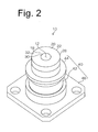
Fig. 2 is a perspective view of a light emitting device (a foil body being omitted) which is an embodiment in accordance with the present invention; -
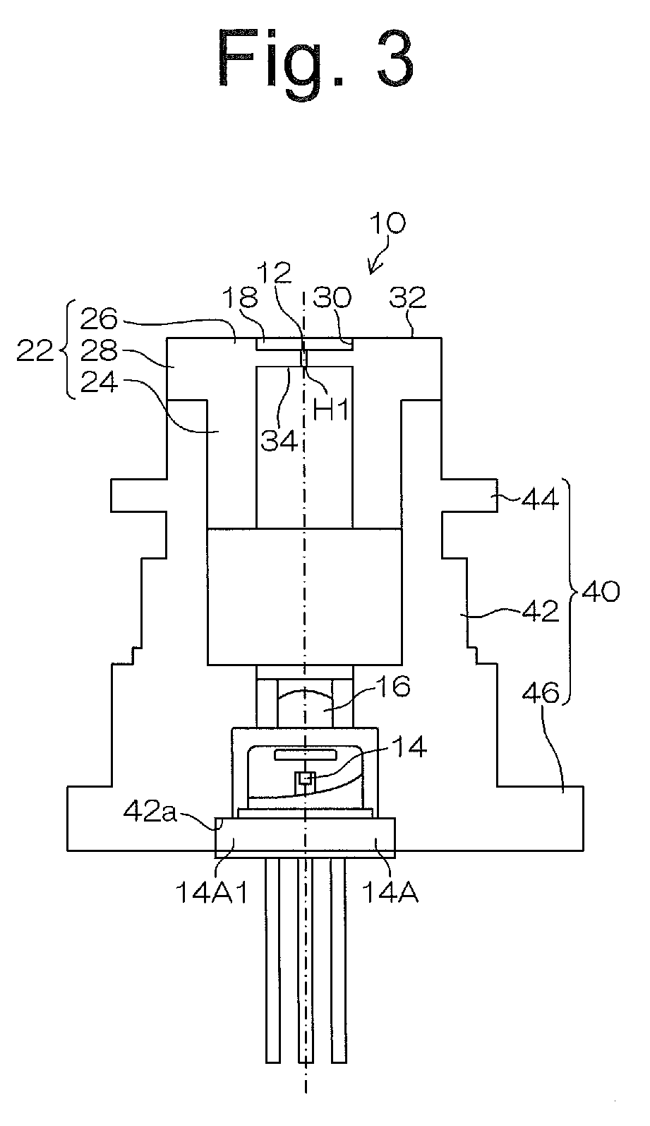
Fig. 3 is a longitudinal sectional view of the light emitting device; -
Fig. 4 is an enlarged partial sectional view near a first through hole; -
Figs. 4A to 4C show the luminance distributions of diffusion light emitted from upper surfaces of three diffusion layers having respective different thicknesses when lower surfaces of the respective diffusion layers are locally irradiated (in a spot-like manner) with laser light condensed by a condenser lens; -
Fig. 6 is a longitudinal sectional view of the light emitting device (modification); -
Fig. 7 is a top view of the light emitting device; -
Figs. 7A to 7C are diagrams illustrating examples of a second through hole formed in the foil body; -
Figs. 8A to 8E are diagrams illustrating modifications of the foil body; -
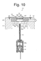
Fig. 10 is a longitudinal sectional view of a light emitting device (modification); -
Fig. 11 is a diagram illustrating a configuration example of a vehicle lamp of so-called direct projection type (also referred to as direct emission type) which includes a projection lens as an optical system configured to control the light from the light emitting device to irradiate in front of a vehicle; and -
Fig. 12 is a diagram illustrating a configuration example of a vehicle lamp of so-called projector type which includes a reflection surface, a shade, and a projection lens as the optical system configured to control the light from the light emitting device to irradiate in front of a vehicle. - A description will now be made below to light emitting devices of the present invention with reference to the accompanying drawings in accordance with exemplary embodiments.
-
Fig. 2 is a perspective view of a light emitting device 10 (afoil body 20 being omitted), an embodiment of the present invention.Fig. 3 is a longitudinal sectional view of the same.Fig. 4 is an enlarged partial sectional view near a first through hole H1. - As shown in
Figs. 2 to 4 , thelight emitting device 10 can include a light-transmittingmember 12, a semiconductorlight emitting element 14, acondenser lens 16, ahigh reflectance member 18, thefoil body 20, and holders for holding such components, composed of afirst holder 22 and asecond holder 40. - The
first holder 22 can be made of metal such as stainless steel. A shown inFig. 3 , thefirst holder 22 can include acylindrical tube portion 24, acircular base portion 26 blocking an upper open end of thetube portion 24, and aflange portion 28 arranged around an upper part of thetube portion 24. - As shown in
Fig. 4 , thebase portion 26 can include asurface 32 including arecess 30, aback surface 34 on the opposite side, and the first through hole H1. The first through hole H1 can penetrate the surface 32 (abottom surface 30a of the recess 30) and theback surface 34. - The light-transmitting
member 12 can be a wavelength conversion member including a diffusion layer 36 (also referred to as a diffusion plate) and awavelength conversion layer 38. Thediffusion layer 36 may be omitted, in which case the entire light-transmittingmember 12 may be composed of thewavelength conversion layer 38. - The
diffusion layer 36 can be a layer including alower surface 36a (corresponding to the first surface according to the present invention) and anupper surface 36b (corresponding to the second surface according to the present invention) on the opposite side. Thelower surface 36a can be fixed to the surface 32 (thebottom surface 30a of the recess 30) so as to cover the first through hole H1. Thediffusion layer 36 can diffuse light (in the present embodiment, laser light) from the semiconductorlight emitting element 14 with which thelower surface 36a (corresponding to the first surface according to the present invention) is locally irradiated (in a spot-like manner). Thediffusion layer 36 can emit the resultant as diffusion light from theupper surface 36b (corresponding to the second surface according to the present invention). - For example, the
diffusion layer 36 can be a layer of rectangular plate shape (for example, a rectangle of 0.4 mm x 0.8 mm with a thickness of 300 µm to 400 µm), made of a composite body (for example, sintered body) of YAG (for example, 25%) and alumina Al2O3 (for example, 75%). The YAG is not doped with an activator (also referred to as luminescent center) such as cerium (Ce). - The light-transmitting member 12 (the
lower surface 36a of the diffusion layer 36) and the surface 32 (thebottom surface 30a of the recess 30) can be bonded, for example, with a transparent adhesive (such as silicone and low-melting glass). Part of thelower surface 36a of thediffusion layer 36 can be exposed from the through hole H1. - The
diffusion layer 36 may be any layer that diffuses the light from the semiconductorlight emitting element 14 with which thelower surface 36a is locally irradiated, and emits the resultant as diffusion light from theupper surface 36b. The shape of thediffusion layer 36 is not limited to the foregoing. - For example, the
diffusion layer 36 may be a cylindrical columnar layer (for example, φ 0.4 mm to 0.8 mm). Thediffusion layer 36 may be a rectangular solid layer (for example, 0.3 mm to 0.6 mm across and 0.6 mm to 2.0 mm long). Layers of other shapes may be used. - The
diffusion layer 36 may be any layer that diffuses the light from the semiconductorlight emitting element 14 with which thelower surface 36a is locally irradiated, and emits the resultant as diffusion light from theupper surface 36b. The material of thediffusion layer 36 is not limited to the foregoing. - For example, the
diffusion layer 36 may be a layer of a composite body of YAG and glass. Thediffusion layer 36 may be a layer of bubble-dispersed alumina Al2O3 (or glass). Layers of other materials may be used. - The
diffusion layer 36 can have the thickness of 300 µm to 400 µm from the following point of view. - The inventor of the present application has confirmed that the thickness h (see
Fig. 4 ) of thediffusion layer 36 can be increased to improve luminance variations of the diffusion light emitted from theupper surface 36b of thediffusion layer 36 for uniform (or generally uniform) luminance distribution. -
Figs. 5A to 5C show the luminance distributions of the diffusion light emitted from theupper surfaces 36b of threediffusion layers 36 having respective different thicknesses h when thelower surface 36a (center) of eachdiffusion layer 36 was locally irradiated (in a spot-like manner) with laser light condensed by thecondenser lens 16. The diffusion layers 36 were made of a composite body of YAG (25%), not doped with cerium (Ce) or other activators, and alumina Al2O3 (75%). The diffusion layer was formed to have a rectangular plate shape with a size of 0.4 mm x 0.8 mm. The laser light from the semiconductorlight emitting element 14 condensed by thecondenser lens 16 was adjusted to an elliptical spot size of approximately 100 µm long and approximately 20 µm to 30 µm across. The side surfaces of the diffusion layers 36 were covered with a high reflectance member, for example, a white resin. - Referring to
Figs. 5A to 5C , it can be seen that luminance variations improve gradually as the thickness h of thediffusion layer 36 increases from 100 µm (seeFig. 5A ) to 200 µm (seeFig. 5B ) to 400 µm (seeFig. 5C ). The luminance distribution becomes uniform (or generally uniform) at the thickness h = 400 µm. The reason is that as the thickness h of thediffusion layer 36 increases, the number of times of scattering (the number of times of scattering due to a difference in refractive index between YAG and alumina Al2O3) of the laser light condensed by the condenser lens 16 (and luminescence caused by the laser light) in thediffusion layer 36 increases to uniformize the laser light. Such uniformized laser light (and luminescence caused by the laser light) is emitted from theupper surface 36b of thediffusion layer 36. - From the foregoing, it is shown that the thickness h of the
diffusion layer 36 can be increased to improve luminance variations of the diffusion light emitted from theupper surface 36b of thediffusion layer 36 and make the luminance distribution uniform (or generally uniform). - Based on the above finding, the thickness h of the
diffusion layer 36 can be set to a thickness such that the diffusion light emitted from theupper surface 36b of thediffusion layer 36 has a uniform (or generally uniform) luminance distribution. Accordingly, in the present embodiment, h preferably falls within the range of 300 µm to 400 µm. Note that the thickness h of thediffusion layer 36 is not limited to 300 µm to 400 µm and may have other values as long as the diffusion effect is obtained. - The
diffusion layer 36 having the above configuration can suppress a drop in efficiency due to luminance saturation and temperature quenching. The reason is that the light from the semiconductor light emitting element 14 (in the present embodiment, laser light) condensed by thecondenser lens 16 is not incident on the wavelength conversion layer 38 (lower surface 38a) as local light. Instead, the light is diffused by thediffusion layer 36 and incident on the wavelength conversion layer 38 (lower surface 38a) as diffusion light having a generally uniform luminance distribution. - As shown in
Fig. 4 , thewavelength conversion layer 38 can be a layer including thelower surface 38a (corresponding to the third surface according to the present invention) joined to theupper surface 36b of thediffusion layer 36 and anupper surface 38b (corresponding to the fourth surface according to the present invention) on the opposite side. Thewavelength conversion layer 38 can convert the wavelength of the diffusion light from thediffusion layer 36 incident on thelower surface 38a, and can emit the resultant from theupper surface 38b. - For example, the
wavelength conversion layer 38 can be a layer with a rectangular plate shape (for example, a rectangle of 0.4 mm x 0.8 mm with a thickness of 80 µm), made of a composite body (for example, sintered body) of activator-doped YAG and alumina Al2O3. Examples of the activator include cerium (Ce). - The
diffusion layer 36 and thewavelength conversion layer 38 can be fixed (joined) so that theupper surface 36b of thediffusion layer 36 and thelower surface 38a of thewavelength conversion layer 38 are in surface contact with each other. For example, if thediffusion layer 36 and thewavelength conversion layer 38 are both made of ceramics, the diffusion layer 36 (upper surface 36b) and the wavelength conversion layer 38 (lower surface 38a) can be fixed (joined) by high-temperature curing theupper surface 36b of thediffusion layer 36 and thelower surface 38a of thewavelength conversion layer 38 in surface contact with each other. If thewavelength conversion layer 38 is a glass phosphor layer, the diffusion layer 36 (upper surface 36b) and the wavelength conversion layer 38 (lower surface 38a) can be fixed (joined) by curing theupper surface 36b of thediffusion layer 36 and thelower surface 38a of thewavelength conversion layer 38 in surface contact with each other. - The
wavelength conversion layer 38 may be any layer that can convert the wavelength of the diffusion light from thediffusion layer 36 incident on thelower surface 38a and can emit the resultant from theupper surface 38b. The shape of thewavelength conversion layer 38 is not limited to the foregoing. - For example, the
wavelength conversion layer 38 may be a circular columnar layer (for example, φ 0.4 mm to 0.8 mm). Thewavelength conversion layer 38 may be a rectangular solid layer (for example, 0.3 mm to 0.6 mm across and 0.6 mm to 2.0 mm long). Layers of other shapes may be used. - The
wavelength conversion layer 38 may be any layer that can convert the wavelength of the diffusion light from thediffusion layer 36 incident on thelower surface 38a and can emit the resultant from theupper surface 38b. The material of thewavelength conversion layer 38 is not limited to the foregoing. - For example, the
wavelength conversion layer 38 may be a layer of a composite body of activator-doped YAG and a glass binder. Examples of the activator include cerium (Ce). Layers of other materials may be used. - As shown in
Fig. 4 , thehigh reflectance member 18 can be a high reflectance member such as a white resin, which is arranged in a space surrounded by the recess 30 (bottom surface 30a andinner wall 30b), the light-transmitting member 12 (side surfaces 12a), and thefoil body 20. For example, thehigh reflectance member 18 can be filled into the space by a dispenser until thehigh reflectance member 18 becomes flush with the top surface of the light-transmitting member 12 (theupper surface 38b of the wavelength conversion layer 38). Thehigh reflectance member 18 can thus cover at least part of the side surfaces 12a of the light-transmittingmember 12. This improves the light output efficiency. The reason is that since the side surfaces 12a of the light-transmittingmember 12 are covered with thehigh reflectance member 18, light emitted from the side surfaces 12a of the light-transmittingmember 12 is reflected from thehigh reflectance member 18 to enter the light-transmittingmember 12 again. As a result, the light output efficiency improves as compared to when the side surfaces 12a of the light-transmittingmember 12 are not covered with thehigh reflectance member 18. If the light output efficiency need not be improved, thehigh reflectance member 18 may be omitted. - The
high reflectance member 18 can be held in the space so as to be less likely to fall off. The reason is that thehigh reflectance member 18 is in close contact with theinner wall 30b and thebottom surface 30a of therecess 30 and the side surfaces 12a of the light-transmittingmember 12. - The
high reflectance member 18 has only to cover at least part of the side surfaces 12a of the light-transmittingmember 12. Thehigh reflectance member 18 may fill the entire space (seeFig. 4 ) or some of the space (seeFig. 6 ). - The side surfaces 12a of the light-transmitting
member 12 are not firmly fixed but covered with the high reflectance member 18 (for example, a white resin) which has elasticity. Each time the light-transmittingmember 12 expands/contracts, the high reflectance member 18 (for example, a white resin) makes an elastic deformation to follow the expansion/contraction. This can suppress the application of stress to the light-transmittingmember 12. As a result, the embrittlement of the light-transmitting member 12 (and the resulting break of the light-transmitting member 12) can be suppressed. - As shown in
Fig. 4 , therecess 30 can be covered with thefoil body 20. -
Fig. 7 is a top view of thelight emitting device 10. - As shown in
Figs. 3 and6 , thefoil body 20 can be a foil body that can include a second through hole H2 for the light emitted from the light-transmitting member 12 (theupper surface 38b of the wavelength conversion layer 38) to pass through, and can have elasticity (spring characteristic) like a Belleville spring. The light-transmittingmember 12 can be sandwiched between thefoil body 20 around the second through hole H2 and the base portion 26 (thebottom surface 30a of the recess 30), with part of the light-transmitting member 12 (theupper surface 38b of the wavelength conversion layer 38) exposed from the second through hole H2 (seeFig. 4 ). - Examples of the
foil body 20 may include metal foil such as stainless steel foil. Copper foil and aluminum foil having a thermal conductivity higher than that of stainless steel foil may be used. At thicknesses below 0.01 mm, thefoil body 20 has little elasticity. At thicknesses above 0.1 mm, part of the light emitted from the light-transmittingmember 12 through the second through hole H2 of thefoil body 20 can be blocked by the inner wall of the second through hole H2. This may lower the light output efficiency. Consequently, thefoil body 20 desirably has a thickness of 0.01 mm to 0.1 mm, and preferably 0.01 mm to 0.05 mm. - The
foil body 20 may be metal foil having a relatively high thermal conductivity (such as copper foil and aluminum foil). Such afoil body 20 can provide a heat dissipation path for the heat generated by the locally irradiating light from the semiconductorlight emitting element 14. As a result, the phosphor excitation efficiency can be increased. - For example, the
foil body 20 and thebase portion 26 can be fixed by welding (resistance welding, YAG welding, and the like). Resistance welding may be used to weld part of thefoil body 20 inside its outer rim to thebase portion 26.Figs. 3 and6 show an example where part (annular part) of thefoil body 20 inside the outer rim can be fixed to the base portion 26 (surface 32) by resistance welding. InFigs. 3 and6 , the welding trace of the resistance welding is designated by the symbol A. YAG welding may be used to weld the outer rim of thefoil body 20 to thebase portion 26. - The
foil body 20 welded as described above is in close contact with the light-transmitting member 12 (near the outer periphery of theupper surface 38b of the wavelength conversion layer 38) and thehigh reflectance member 18 at room temperature (seeFig. 4 ). - The
foil body 20 of the foregoing configuration can make an elastic deformation to follow expansion/contraction of the high reflectance member 18 (for example, white resin) each time thehigh reflectance member 18 expands/contracts because of the heat generated by the locally irradiating light from the semiconductor light emitting element 14 (for example, semiconductor laser light source). Thefoil body 20 can therefore securely hold the light-transmittingmember 12. - The
foil body 20 has only to have elasticity, and is not limited to the foregoing. For example, aside from metal foil, thefoil body 20 may be a graphite sheet having an extremely high thermal conductivity. Foil of other materials may be used. - The
foil body 20 may have the same thickness overall. Thefoil body 20 may have different thicknesses in part. For example, thefoil body 20 may have a greater thickness in the portion to be welded than in the other potions. This can secure a greater welding margin, so that thefoil body 20 and thebase portion 26 can be more firmly welded (fixed) to each other. - The
foil body 20 may have a greater thickness around the through hole 2 (the portion to press the light-transmitting member 12) that in the other portions. Thefoil body 20 may be made thinner in a portion where elasticity is needed than in the other potions. - For example, the
foil body 20 can be manufactured by the following manner. - Initially, rolled metal foil (for example, stainless steel foil) is manufactured. The metal foil desirably has a thickness of 0.01 mm to 0.1 mm, and preferably 0.01 mm to 0.05 mm.
- The rolled metal foil is then cut into a predetermined shape. For example, according to the shape of the base portion 26 (for example, circular shape), the metal foil is cut into a circular shape.
- Next, a second through hole H2 of desired shape is formed in the cut metal foil of the predetermined shape, for example, by press punching.
- In such a manner, the
foil body 20 including the second through hole H2 can be manufactured. -
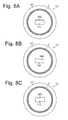
Figs. 8A to 8C show examples of the second through hole H2 formed in thefoil body 20. - Forming the second through hole H2 in an arbitrary shape (for example, see
Figs. 8A to 8C ) can form a light emitting surface (constituted by part of theupper surface 38b of thewavelength conversion layer 38 exposed from the second through hole H2) of arbitrary shape. The outline of the light emitting surface is defined by the shape of the second through hole H2. - For example, the second through hole H2 may be formed in an appropriate shape (for example, see
Figs. 8A to 8C ) according to the shape, size, and the like of the intended light distributed pattern. In such a manner, a light emitting surface having a shape suitable for a desired light distribution pattern (for example, low-beam light distribution pattern) can be easily formed. -
Fig. 8A shows an example where the second through hole H2 is formed in a horizontal rectangular shape. Such a shape is intended to constitute a light emitting surface equivalent to a horizontal rectangular one used for a typical projector type vehicle headlight etc. -
Fig. 8B shows an example where the second through hole H2 is formed in a horizontal rectangular shape with a step portion corresponding to a cutoff line in either one of long sides. Such a shape is intended to constitute a light emitting surface suitable to form a low-beam light distribution pattern including a cutoff line at the upper edge. -
Fig. 8C shows an example where the second through hole H2 is formed in a horizontal rectangular shape with notched portions on both long sides. - The shape of the second through hole H2 is not limited to the foregoing. For example, circular, elliptical, and various other shapes may be used.
-
Figs. 9A to 9E show modifications of thefoil body 20. - The
foil body 20 is not limited to a flat shape like shown inFigs. 4 and9A . For example, as shown inFig. 9B , thefoil body 20 may be pressed or squeezed around the second through hole H2 so that thefoil body 20 has a convex shape (or concave shape) around the second through hole H2. - With such a configuration, the light-transmitting
member 12 can be sandwiched from both the side surfaces 12a. - As shown in
Figs. 9C and 9D , thefoil body 20 may include reflection surfaces 20a for controlling the light passing through the second through hole H2. With such a configuration, the distribution of the light passing through the second through hole H2 can be controlled to an intended direction to form an intended light distribution pattern (for example, low-beam light distribution pattern). -
Figs. 9C and 9D show examples where thefoil body 20 and the reflection surfaces 20a are integrally formed. The foil body 20 (metal foil) is bent in the portions continuous with the periphery of the second through hole H2, whereby the reflection surfaces 20a for controlling the light passing through the second through hole H2 are formed around the second through hole H2. For higher reflectance, mirror finishing (for example, aluminum deposition) may be applied to the portions used as the reflection surfaces 20a. Alternatively, additional mirror members may be bonded to the portions by adhesion etc. - As shown in
Fig. 9E , thefoil body 20 may be shaped to include curved portions (for example, accordion-like curved portions) for improved elasticity. - The
second holder 40 can be made of metal such as stainless steel. As shown inFig. 3 , thesecond holder 40 can include acylindrical tube portion 42, anupper flange portion 44 arranged around an upper part of thetube portion 42, and alower flange portion 46 arranged around a lower part of thetube portion 42. - The
first holder 22 can be fixed to thesecond holder 40 so that thetube portion 24 is inserted into thetube portion 42 of theholder 40 through a top opening of thetube portion 42, with theflange portion 28 of thefirst holder 22 and the top end of thetube portion 42 of thesecond holder 40 in contact with each other. - The semiconductor
light emitting element 14 can be a semiconductor light emitting element that emits light to pass through the first through hole H1 and for the light-transmitting member 12 (thelower surface 36a of the diffusion layer 36) to be irradiated with. Examples of the semiconductorlight emitting element 14 may include a semiconductor laser light source such as a laser diode (LD) having a blue emission wavelength (around 450 nm). In the present embodiment, as shown inFig. 3 , the semiconductorlight emitting element 14 can be packaged to constitute a can-type semiconductorlaser light source 14A. - The semiconductor
light emitting element 14 is not limited to a laser diode, and may be a light-emitting diode (LED). The emission wavelength of the semiconductorlight emitting element 14 is not limited to the blue region (around 450 nm). For example, a near ultraviolet region (around 405 nm) may be used. If the semiconductorlight emitting element 14 has an emission wavelength in the near ultraviolet region (around 405 nm), thewavelength conversion layer 38 can use three color phosphors in blue, green, and red, or two color phosphors in blue and yellow. - The semiconductor
laser light source 14A can be inserted into thetube portion 42 of thesecond holder 40 through a bottom opening of thetube portion 42. The semiconductorlaser light source 14A can be fixed to thesecond holder 40 so that a flange portion 14A1 of the semiconductorlaser light source 14A and astep portion 42a of thetube portion 42 are in contact with each other. - The
condenser lens 16 can be an optical system that can condense the light from the semiconductorlight emitting element 14 and can locally irradiate the light-transmitting member 12 (thelower surface 36a of the diffusion layer 36) with the light. Thecondenser lens 16 can be held by the second older 40 and arranged between the light-transmittingmember 12 and the semiconductorlight emitting element 14. - In the
light emitting device 10 having the above configuration, the light from the semiconductorlight emitting element 14 can be condensed by thecondenser lens 16 and can pass through the first through hole H1. The light-transmitting member 12 (thelower surface 36a of the diffusion layer 36) located at a distance from the semiconductorlight emitting element 14 can be locally irradiated (in a spot-like manner) with the light. The spot size can be adjusted, for example, to an elliptical shape of approximately 100 µm long and approximately 20 µm to 30 µm across. The light with which the light-transmitting member 12 (thelower surface 36a of the diffusion layer 36) is locally irradiated (in a spot-like manner) can be diffused inside thediffusion layer 36 and emitted from theupper surface 36b of thediffusion layer 36 as diffusion light having a uniform (or generally uniform) luminance distribution. The diffusion light can be incident on thelower surface 38a of thewavelength conversion layer 38. - The
wavelength conversion layer 38 on which the diffusion light from thediffusion layer 36 is incident can emit white light. The white light can be obtained by color mixture of the transmitted diffusion light from thediffusion layer 36 and light (luminescence) that is emitted due to excitation by the diffusion light from thediffusion layer 36. The white light can pass through the second through hole H2 formed in thefoil body 20 and can be taken outside. - As has been described above, the
light emitting device 10 according to the present embodiment can provide the following advantages. - Firstly, the light-transmitting
member 12 can be prevented from falling off even if the adhesive or the like bonding the light-transmitting member 12 (thelower surface 36a of the diffusion layer 36) to the surface 32 (thebottom surface 30a of the recess 30) degrades. This advantage results from the fact that the light-transmittingmember 12 is sandwiched between the foil body 20 (around the second through hole H2) and the base portion 26 (seeFig. 3 ). - Secondly, the embrittlement of the light-transmitting member 12 (and the resulting break of the light-transmitting member 12) can be suppressed while the light-transmitting
member 12 repeats expansion and contraction because of heat generated by the locally irradiating light from the semiconductor light emitting element 14 (for example, semiconductor laser light source). This advantage results from the fact that theelastic foil body 20 is used as a member for sandwiching (fixing) the light-transmittingmember 12. - More specifically, suppose that the light-transmitting
member 12 is firmly fixed by using a member having no elasticity (or member having little elasticity) as the member for sandwiching (fixing) the light-transmittingmember 12. In such a case, the light-transmittingmember 12 undergoes stress each time the light-transmittingmember 12 expands/contracts. As a result, the embrittlement of the light-transmitting member 12 (and the resulting break of the light-transmitting member 12) is facilitated. - In contrast, according to the
light emitting device 10 of the present embodiment, theelastic foil body 20 is used as the member for sandwiching (fixing) the light-transmittingmember 12. Each time the light-transmittingmember 12 expands/contacts, thefoil body 20 can make an elastic deformation to follow the expansion/contraction, whereby the application of stress to the light-transmittingmember 12 can be suppressed. Consequently, the embrittlement of the light-transmitting member 12 (and the resulting break of the light-transmitting member 12) can be suppressed. - Thirdly, the light output efficiency can be increased. This advantage results from the fact that the
foil body 20 having a substantially negligible thickness is used as the member for sandwiching (fixing) the light-transmittingmember 12. - More specifically, suppose that the light-transmitting
member 12 is sandwiched (fixed) by using a member having more than a certain thickness. In such a case, part of the light emitted from the light-transmittingmember 12 through the second through hole H2 is blocked by the inner wall of the second through hole H2. This lowers the light output efficiency. - In contrast, according to the
light emitting device 10 of the present embodiment, thefoil body 20 having a substantially negligible thickness can be used as the member for sandwiching (fixing) the light-transmittingmember 12. The light emitted from the light-transmittingmember 12 through the second through hole H2 will hardly be blocked by the inner fall of the second through hole H2. As a result, the light output efficiency can be increased. - Fourthly, the second through hole H2 can be formed in an arbitrary shape. This advantage results from the fact that the second through hole H2 is formed in the
foil body 20 which is easily processable. - Fifthly, a light emission surface having an arbitrary shape (constituted by part of the
upper surface 38b of thewavelength conversion layer 38 exposed from the second through hole H2) can be formed. The outline of the light emission surface is defined by the shape of the second through hole H2. - For example, the second through hole H2 can be formed in an appropriate shape (for example, see
Figs. 7A to 7C ) according to the shape, size, and the like of an intended light distribution pattern. In such a manner, a light emission surface having a shape suitable for a predetermined light distribution pattern (for example, low-beam light distribution pattern) can be easily formed. - Next, a modification will be described.
-
Fig. 10 is a longitudinal section view of a light emitting device 10 (modification). - In the foregoing embodiment, the condenser lens 16 (see
Fig. 3 ) has been described as the optical system for condensing the light from the semiconductorlight emitting element 14 and locally irradiating the light-transmitting member 12 (thelower surface 36a of the diffusion layer 36) with the light. The present invention is not limited thereto. - For example, the
condenser lens 16 serving as the optical system for condensing the light from the semiconductorlight emitting element 14 and locally irradiating the light-transmitting member 12 (thelower surface 36a of the diffusion layer 36) with the light may be replaced with an optical system such as shown inFig. 10 . The optical system shown inFig. 10 can include thecondenser lens 16 and alight guide 48. Thecondenser lens 16 can condense the light from the semiconductorlight emitting element 14. Thelight guide 48 can guide the light from the semiconductorlight emitting element 14 condensed by thecondenser lens 16 and can locally irradiate the light-transmitting member 12 (thelower surface 36a of the diffusion layer 36) with the light. - Examples of the
light guide 48 may include an optical fiber having a center core (for example, with a core diameter of 0.2 mm) and a surrounding clad, neither of which is shown. The core has a refractive index higher than that of the clad. The laser light introduced into thelight guide 48 through anend 48a of the light guide 48 (the laser light from the semiconductorlight emitting element 14 condensed by the condenser lens 16) can be guided to theother end 48b of thelight guide 48 as confined within the core by utilizing the total reflection at the interface between the core and the clad. The light can be emitted from theother end 48b, and the light-transmitting member 12 (thelower surface 36a of the diffusion layer 36) located at a distance from the semiconductorlight emitting element 14 can be locally irradiated with the light. - The light with which the
lower surface 36a of thediffusion layer 36 is locally irradiated (in a spot-like manner) can be diffused inside thediffusion layer 36 and emitted from theupper surface 36b of thediffusion layer 36 as diffusion light having a uniform (or generally uniform) luminance distribution. The diffusion light can be incident on thelower surface 38a of thewavelength conversion layer 38. - The
wavelength conversion layer 38 on which the diffusion light from thediffusion layer 36 is incident can emit white light. The white light can be caused by color mixture of the transmitted diffusion light from thediffusion layer 36 and light that is emitted due to excitation by the diffusion light from thediffusion layer 36. The white light can pass through the second through hole H2 of thefoil body 20 and can be taken outside. - The
light emitting device 10 of the present modification can provide the same effects as those of the foregoing embodiment. - Next, examples of a vehicle lamp (for example, vehicle headlight) using the
light emitting device 10 having the above configuration will be described. -
Fig. 11 shows an example of avehicle lamp 50 of so-called direct projection type (also referred to as direct emission type). Thevehicle lamp 50 can employ aprojection lens 52 as an optical system configured to control the light from thelight emitting device 10 and irradiate in front of the vehicle. Theprojection lens 52 and thelight emitting device 10 arranged behind theprojection lens 52 can be held in a predetermined positional relationship by aholder 54. -
Fig. 12 shows an example of avehicle lamp 60 of so-called projector type. Thevehicle lamp 60 can include areflection surface 62, ashade 64, and aprojection lens 66 as the optical system configured to control the light from thelight emitting device 10 and irradiate in front of the vehicle. Thereflection surface 62, theshade 64, theprojection lens 66, and thelight emitting device 10 can be held in a predetermined positional relationship by aholder 68. - Aside from vehicle lamps, the
light emitting device 10 may be used, for example, as a projection light, indoor lighting, outdoor lighting, and a projector light source.
Claims (11)
- A light emitting device (10) characterized by comprising:a base portion (26) configured to include a surface (32), a back surface (34) on the opposite side thereto, and a first through hole (H1) penetrating the surface (32) and the back surface (34);a light-transmitting member (12) that is fixed to the surface (32) so as to cover the first through hole (H1);a semiconductor light emitting element (14) configured to emit light to pass through the first through hole (H1) and for the light-transmitting member (12) to be irradiated with;an optical system (16) configured to condense the light from the semiconductor light emitting element (14) and locally irradiate the light-transmitting member (12) with the light; anda foil body (20) configured to include a second through hole (H2) for light emitted from the light-transmitting member (12) to pass through and has elasticity, the light-transmitting member (12) being sandwiched between the foil body (20) around the second through hole (H2) and the base portion (26) with part of the light-transmitting member (12) exposed from the second through hole (H2).
- The light emitting device (10) according to claim 1, characterized by further comprising a high reflectance member (18) configured to cover at least part of a side surface of the light-transmitting member (12).
- The light emitting device (10) according to claim 2, characterized in that the high reflectance member (18) is a white resin.
- The light emitting device (10) according to any one of claims 1 to 3, characterized in that
the surface (32) includes a recess (30) including a bottom surface (30a) in which the first through hole (H1) is formed;
the light-transmitting member (12) is fixed to the bottom surface (30a) of the recess (30) so as to cover the first through hole (H1); and
the high reflectance member (18) is arranged in a space defined by an inner wall and the bottom surface (30a) of the recess (30), the side surface of the light-transmitting member (12), and the foil body (20). - The light emitting device (10) according to any one of claims 1 to 4, characterized in that
the light-transmitting member (12) is a wavelength conversion member including a diffusion layer (36) and a wavelength conversion layer (38);
the diffusion layer (36) includes a first surface (36a) fixed to the surface (32) so as to cover the first through hole (H1) and a second surface (36b) on the opposite side, and diffuses the light from the semiconductor light emitting element (14) with which the first surface (36a) is irradiated, so as to emit the resultant as diffusion light from the second surface (36b); and
the wavelength conversion layer (38) includes a third surface (38a) joined to the second surface (36b) and a fourth surface (38b) on the opposite side, and converts a wavelength of the diffusion light incident on the third surface (38a), so as to emit the resultant from the fourth surface (38b). - The light emitting device (10) according to any one of claims 1 to 5, characterized in that the foil body (20) is a metal foil.
- The light emitting device (10) any one of claims 1 to 6, characterized in that the foil body (20) includes a reflection surface configured to control the light passing through the second through hole (H2).
- The light emitting device (10) according to claim 5, characterized in that the diffusion layer (36) has a thickness set so that the diffusion light emitted from the second surface (36b) has a generally uniform luminance distribution.
- The light emitting device (10) any one of claims 1 to 8, characterized in that the optical system (16) includes a condenser lens (16) that can condense the light from the semiconductor light emitting element (14) and locally irradiate the light-transmitting member (12) with the light through the first through hole (H1).
- The light emitting device (10) any one of claims 1 to 8, characterized in that the optical system includes a condenser lens (16) that condenses the light from the semiconductor light emitting element (14), and a light guide (48) that can guide the light from the semiconductor light emitting element (14) condensed by the condenser lens and locally irradiate the light-transmitting member (12) with the light.
- A vehicle lamp (50, 60) characterized by comprising:the light emitting device (10) according to any one of claims 1 to 10; andan optical system configured to control light from the light emitting device (10) to irradiate in front of a vehicle.
Applications Claiming Priority (1)
| Application Number | Priority Date | Filing Date | Title |
|---|---|---|---|
| JP2012264408A JP6119214B2 (en) | 2012-12-03 | 2012-12-03 | Light emitting device and vehicle lamp |
Publications (2)
| Publication Number | Publication Date |
|---|---|
| EP2738888A2 true EP2738888A2 (en) | 2014-06-04 |
| EP2738888A3 EP2738888A3 (en) | 2018-03-28 |
Family
ID=49884873
Family Applications (1)
| Application Number | Title | Priority Date | Filing Date |
|---|---|---|---|
| EP13020131.2A Withdrawn EP2738888A3 (en) | 2012-12-03 | 2013-12-02 | Light emitting device and vehicle lamp |
Country Status (3)
| Country | Link |
|---|---|
| US (1) | US9080732B2 (en) |
| EP (1) | EP2738888A3 (en) |
| JP (1) | JP6119214B2 (en) |
Cited By (4)
| Publication number | Priority date | Publication date | Assignee | Title |
|---|---|---|---|---|
| EP3021433A1 (en) * | 2014-11-11 | 2016-05-18 | Stanley Electric Co., Ltd. | Semiconductor light-emitting apparatus and vehicle headlight including the same |
| DE102015204817A1 (en) | 2015-03-17 | 2016-09-22 | Osram Gmbh | Conversion device for converting radiation, luminaire arrangement and method for producing a conversion device |
| EP3267095A1 (en) * | 2016-06-22 | 2018-01-10 | LG Innotek Co., Ltd. | Phosphor plate and lighting device including the same |
| US10343768B2 (en) | 2014-12-30 | 2019-07-09 | Airbus Operations (S.A.S.) | Landing gear well roof |
Families Citing this family (16)
| Publication number | Priority date | Publication date | Assignee | Title |
|---|---|---|---|---|
| JP2015005439A (en) * | 2013-06-21 | 2015-01-08 | スタンレー電気株式会社 | Vehicle headlamp and optical fiber bundle used in vehicle headlamp |
| KR101592649B1 (en) * | 2013-12-24 | 2016-02-12 | 현대자동차주식회사 | Laser optical system for head lamp |
| KR101620193B1 (en) * | 2014-09-26 | 2016-05-12 | 현대자동차주식회사 | Laser optical system for head lamp |
| JP6296024B2 (en) * | 2015-08-28 | 2018-03-20 | 日亜化学工業株式会社 | Semiconductor laser device |
| WO2017038164A1 (en) * | 2015-09-03 | 2017-03-09 | シャープ株式会社 | Light-emitting device |
| KR101795229B1 (en) * | 2016-03-31 | 2017-11-08 | 현대자동차주식회사 | Lamp apparatus for a vehicle |
| JP6766617B2 (en) * | 2016-11-29 | 2020-10-14 | セイコーエプソン株式会社 | Light source device and projector |
| JP6925174B2 (en) * | 2017-06-05 | 2021-08-25 | スタンレー電気株式会社 | Wavelength converter |
| JP6881248B2 (en) * | 2017-11-14 | 2021-06-02 | 日亜化学工業株式会社 | Optical member holding device, manufacturing method of optical member holding device and semiconductor laser device |
| JP6702349B2 (en) * | 2018-03-27 | 2020-06-03 | 日亜化学工業株式会社 | Light emitting device |
| DE102018107213B4 (en) * | 2018-03-27 | 2025-05-22 | HELLA GmbH & Co. KGaA | Lighting device for vehicles |
| DE102020106594A1 (en) * | 2019-03-12 | 2020-09-17 | Nichia Corporation | METHOD OF MANUFACTURING AN OPTICAL ELEMENT, OPTICAL ELEMENT, AND LIGHT Emitting Device |
| JP6954329B2 (en) | 2019-06-25 | 2021-10-27 | セイコーエプソン株式会社 | Wavelength converters, light source devices and projectors |
| JP7294089B2 (en) * | 2019-11-28 | 2023-06-20 | セイコーエプソン株式会社 | Light source device and projector |
| JP7100813B2 (en) * | 2020-09-09 | 2022-07-14 | カシオ計算機株式会社 | Light source device and projection device |
| JP7622500B2 (en) | 2021-03-25 | 2025-01-28 | セイコーエプソン株式会社 | Wavelength conversion device, light source device, and projector |
Citations (1)
| Publication number | Priority date | Publication date | Assignee | Title |
|---|---|---|---|---|
| JP2010165834A (en) | 2009-01-15 | 2010-07-29 | Nichia Corp | Light emitting device |
Family Cites Families (14)
| Publication number | Priority date | Publication date | Assignee | Title |
|---|---|---|---|---|
| JPH1016639A (en) * | 1996-07-02 | 1998-01-20 | S S Ltd:Kk | Vehicle lighting |
| JP3486680B2 (en) * | 2001-08-10 | 2004-01-13 | 株式会社ネクスト | Semiconductor laser projector unit |
| JP5083592B2 (en) * | 2005-12-12 | 2012-11-28 | 日亜化学工業株式会社 | Optical component, light conversion member, and light emitting device |
| JP5228412B2 (en) * | 2006-11-21 | 2013-07-03 | 日亜化学工業株式会社 | Semiconductor light emitting device |
| JP2011123379A (en) * | 2009-12-11 | 2011-06-23 | Asahi Kasei E-Materials Corp | Light beam control unit, direct backlight apparatus and liquid crystal display apparatus |
| JP2011243369A (en) * | 2010-05-17 | 2011-12-01 | Sharp Corp | Light-emitting device, illumination device, and vehicle headlight |
| JP5285688B2 (en) * | 2010-12-28 | 2013-09-11 | シャープ株式会社 | Light emitting device, lighting device, and vehicle headlamp |
| US8833975B2 (en) * | 2010-09-07 | 2014-09-16 | Sharp Kabushiki Kaisha | Light-emitting device, illuminating device, vehicle headlamp, and method for producing light-emitting device |
| US8691890B2 (en) * | 2010-10-22 | 2014-04-08 | Panasonic Corporation | Unsaturated polyester resin composition for use in LED reflector, and LED reflector and LED luminaire using said composition |
| WO2012124587A1 (en) * | 2011-03-16 | 2012-09-20 | シャープ株式会社 | Wavelength conversion member, production method for same, light-emitting device, illumination device, and headlight |
| JP2012221634A (en) * | 2011-04-05 | 2012-11-12 | Sharp Corp | Lighting system and headlamp |
| EP2840301A3 (en) * | 2011-12-20 | 2015-12-09 | Stanley Electric Co., Ltd. | Light emitting device, vehicle light and vehicle |
| JP6061130B2 (en) * | 2012-09-27 | 2017-01-18 | スタンレー電気株式会社 | Light emitting device |
| JP6056117B2 (en) * | 2012-12-06 | 2017-01-11 | スタンレー電気株式会社 | Light emitting device and vehicle lamp |
-
2012
- 2012-12-03 JP JP2012264408A patent/JP6119214B2/en active Active
-
2013
- 2013-12-02 EP EP13020131.2A patent/EP2738888A3/en not_active Withdrawn
- 2013-12-03 US US14/095,504 patent/US9080732B2/en active Active
Patent Citations (1)
| Publication number | Priority date | Publication date | Assignee | Title |
|---|---|---|---|---|
| JP2010165834A (en) | 2009-01-15 | 2010-07-29 | Nichia Corp | Light emitting device |
Cited By (6)
| Publication number | Priority date | Publication date | Assignee | Title |
|---|---|---|---|---|
| EP3021433A1 (en) * | 2014-11-11 | 2016-05-18 | Stanley Electric Co., Ltd. | Semiconductor light-emitting apparatus and vehicle headlight including the same |
| US9903542B2 (en) | 2014-11-11 | 2018-02-27 | Stanley Electric Co., Ltd. | Semiconductor light-emitting apparatus and vehicle headlight |
| US10343768B2 (en) | 2014-12-30 | 2019-07-09 | Airbus Operations (S.A.S.) | Landing gear well roof |
| DE102015204817A1 (en) | 2015-03-17 | 2016-09-22 | Osram Gmbh | Conversion device for converting radiation, luminaire arrangement and method for producing a conversion device |
| EP3267095A1 (en) * | 2016-06-22 | 2018-01-10 | LG Innotek Co., Ltd. | Phosphor plate and lighting device including the same |
| US10928035B2 (en) | 2016-06-22 | 2021-02-23 | Lg Innotek Co., Ltd. | Phosphor plate and lighting device including the same |
Also Published As
| Publication number | Publication date |
|---|---|
| JP2014110173A (en) | 2014-06-12 |
| US9080732B2 (en) | 2015-07-14 |
| US20140153276A1 (en) | 2014-06-05 |
| EP2738888A3 (en) | 2018-03-28 |
| JP6119214B2 (en) | 2017-04-26 |
Similar Documents
| Publication | Publication Date | Title |
|---|---|---|
| US9080732B2 (en) | Light emitting device and vehicle lamp | |
| US9316372B2 (en) | Light emitting device and vehicle lamp | |
| JP6061130B2 (en) | Light emitting device | |
| JP6177596B2 (en) | Light emitting device | |
| JP6135032B2 (en) | Light emitting device, vehicle lamp, and stress relief part molding method | |
| JP2012099362A (en) | Light emitting device | |
| JP5172987B2 (en) | Light emitting device, lighting device and headlamp | |
| JPWO2007105647A1 (en) | Light emitting device | |
| JP2016066480A (en) | Light emitting device | |
| JP2010232044A (en) | Vehicle lighting | |
| US20120057364A1 (en) | Light-emitting device, illuminating device, vehicle headlamp, and method for producing light-emitting device | |
| JP2008305936A (en) | Semiconductor light emitting device | |
| US20170256685A1 (en) | A light emitting device | |
| EP2559077B1 (en) | Lighting device | |
| JP2016058624A (en) | Light emitting device | |
| JP5994537B2 (en) | Luminescent bulb and vehicle lamp | |
| JP6162537B2 (en) | LIGHT SOURCE DEVICE, LIGHTING DEVICE, AND VEHICLE LIGHT | |
| JP2009187773A (en) | Lighting device | |
| JP6593189B2 (en) | Light source device | |
| JP2012221633A (en) | Lighting device and headlamp | |
| CN212273733U (en) | Laser light-emitting device and lamp | |
| JP2014211982A (en) | Light emitting device and vehicle lighting tool | |
| JP2017228390A (en) | Lighting device | |
| JP5742629B2 (en) | LIGHT EMITTING DEVICE AND LIGHTING APPARATUS HAVING THE SAME | |
| JP6583781B2 (en) | Lighting device |
Legal Events
| Date | Code | Title | Description |
|---|---|---|---|
| PUAI | Public reference made under article 153(3) epc to a published international application that has entered the european phase |
Free format text: ORIGINAL CODE: 0009012 |
|
| 17P | Request for examination filed |
Effective date: 20131202 |
|
| AK | Designated contracting states |
Kind code of ref document: A2 Designated state(s): AL AT BE BG CH CY CZ DE DK EE ES FI FR GB GR HR HU IE IS IT LI LT LU LV MC MK MT NL NO PL PT RO RS SE SI SK SM TR |
|
| AX | Request for extension of the european patent |
Extension state: BA ME |
|
| PUAL | Search report despatched |
Free format text: ORIGINAL CODE: 0009013 |
|
| AK | Designated contracting states |
Kind code of ref document: A3 Designated state(s): AL AT BE BG CH CY CZ DE DK EE ES FI FR GB GR HR HU IE IS IT LI LT LU LV MC MK MT NL NO PL PT RO RS SE SI SK SM TR |
|
| AX | Request for extension of the european patent |
Extension state: BA ME |
|
| RIC1 | Information provided on ipc code assigned before grant |
Ipc: H01S 5/00 20060101ALN20180219BHEP Ipc: F21S 8/10 00000000ALI20180219BHEP Ipc: H01L 33/58 20100101ALN20180219BHEP Ipc: H01S 5/022 20060101AFI20180219BHEP |
|
| RIC1 | Information provided on ipc code assigned before grant |
Ipc: H01L 33/58 20100101ALN20180219BHEP Ipc: H01S 5/022 20060101AFI20180219BHEP Ipc: H01S 5/00 20060101ALN20180219BHEP Ipc: F21S 8/10 20181130ALI20180219BHEP |
|
| RIC1 | Information provided on ipc code assigned before grant |
Ipc: H01L 33/58 20100101ALN20180219BHEP Ipc: H01S 5/022 20060101AFI20180219BHEP Ipc: H01S 5/00 20060101ALN20180219BHEP Ipc: F21S 8/10 20060101ALI20180219BHEP |
|
| STAA | Information on the status of an ep patent application or granted ep patent |
Free format text: STATUS: THE APPLICATION IS DEEMED TO BE WITHDRAWN |
|
| 18D | Application deemed to be withdrawn |
Effective date: 20180929 |