EP2725881A1 - Chip on film and display device including the same - Google Patents
Chip on film and display device including the same Download PDFInfo
- Publication number
- EP2725881A1 EP2725881A1 EP13190371.8A EP13190371A EP2725881A1 EP 2725881 A1 EP2725881 A1 EP 2725881A1 EP 13190371 A EP13190371 A EP 13190371A EP 2725881 A1 EP2725881 A1 EP 2725881A1
- Authority
- EP
- European Patent Office
- Prior art keywords
- film
- chip
- driving
- electromagnetic wave
- wave blocking
- Prior art date
- Legal status (The legal status is an assumption and is not a legal conclusion. Google has not performed a legal analysis and makes no representation as to the accuracy of the status listed.)
- Granted
Links
Images



Classifications
-
- H—ELECTRICITY
- H05—ELECTRIC TECHNIQUES NOT OTHERWISE PROVIDED FOR
- H05K—PRINTED CIRCUITS; CASINGS OR CONSTRUCTIONAL DETAILS OF ELECTRIC APPARATUS; MANUFACTURE OF ASSEMBLAGES OF ELECTRICAL COMPONENTS
- H05K9/00—Screening of apparatus or components against electric or magnetic fields
-
- H—ELECTRICITY
- H05—ELECTRIC TECHNIQUES NOT OTHERWISE PROVIDED FOR
- H05K—PRINTED CIRCUITS; CASINGS OR CONSTRUCTIONAL DETAILS OF ELECTRIC APPARATUS; MANUFACTURE OF ASSEMBLAGES OF ELECTRICAL COMPONENTS
- H05K1/00—Printed circuits
- H05K1/02—Details
- H05K1/0213—Electrical arrangements not otherwise provided for
- H05K1/0216—Reduction of cross-talk, noise or electromagnetic interference
- H05K1/0218—Reduction of cross-talk, noise or electromagnetic interference by printed shielding conductors, ground planes or power plane
- H05K1/0224—Patterned shielding planes, ground planes or power planes
-
- H—ELECTRICITY
- H10—SEMICONDUCTOR DEVICES; ELECTRIC SOLID-STATE DEVICES NOT OTHERWISE PROVIDED FOR
- H10K—ORGANIC ELECTRIC SOLID-STATE DEVICES
- H10K59/00—Integrated devices, or assemblies of multiple devices, comprising at least one organic light-emitting element covered by group H10K50/00
- H10K59/10—OLED displays
- H10K59/12—Active-matrix OLED [AMOLED] displays
- H10K59/126—Shielding, e.g. light-blocking means over the TFTs
-
- H—ELECTRICITY
- H10—SEMICONDUCTOR DEVICES; ELECTRIC SOLID-STATE DEVICES NOT OTHERWISE PROVIDED FOR
- H10W—GENERIC PACKAGES, INTERCONNECTIONS, CONNECTORS OR OTHER CONSTRUCTIONAL DETAILS OF DEVICES COVERED BY CLASS H10
- H10W42/00—Arrangements for protection of devices
- H10W42/20—Arrangements for protection of devices protecting against electromagnetic or particle radiation, e.g. light, X-rays, gamma-rays or electrons
-
- H—ELECTRICITY
- H10—SEMICONDUCTOR DEVICES; ELECTRIC SOLID-STATE DEVICES NOT OTHERWISE PROVIDED FOR
- H10W—GENERIC PACKAGES, INTERCONNECTIONS, CONNECTORS OR OTHER CONSTRUCTIONAL DETAILS OF DEVICES COVERED BY CLASS H10
- H10W70/00—Package substrates; Interposers; Redistribution layers [RDL]
- H10W70/60—Insulating or insulated package substrates; Interposers; Redistribution layers
- H10W70/67—Insulating or insulated package substrates; Interposers; Redistribution layers characterised by their insulating layers or insulating parts
- H10W70/688—Flexible insulating substrates
-
- H—ELECTRICITY
- H10—SEMICONDUCTOR DEVICES; ELECTRIC SOLID-STATE DEVICES NOT OTHERWISE PROVIDED FOR
- H10W—GENERIC PACKAGES, INTERCONNECTIONS, CONNECTORS OR OTHER CONSTRUCTIONAL DETAILS OF DEVICES COVERED BY CLASS H10
- H10W72/00—Interconnections or connectors in packages
- H10W72/20—Bump connectors, e.g. solder bumps or copper pillars; Dummy bumps; Thermal bumps
-
- G—PHYSICS
- G02—OPTICS
- G02F—OPTICAL DEVICES OR ARRANGEMENTS FOR THE CONTROL OF LIGHT BY MODIFICATION OF THE OPTICAL PROPERTIES OF THE MEDIA OF THE ELEMENTS INVOLVED THEREIN; NON-LINEAR OPTICS; FREQUENCY-CHANGING OF LIGHT; OPTICAL LOGIC ELEMENTS; OPTICAL ANALOGUE/DIGITAL CONVERTERS
- G02F1/00—Devices or arrangements for the control of the intensity, colour, phase, polarisation or direction of light arriving from an independent light source, e.g. switching, gating or modulating; Non-linear optics
- G02F1/01—Devices or arrangements for the control of the intensity, colour, phase, polarisation or direction of light arriving from an independent light source, e.g. switching, gating or modulating; Non-linear optics for the control of the intensity, phase, polarisation or colour
- G02F1/13—Devices or arrangements for the control of the intensity, colour, phase, polarisation or direction of light arriving from an independent light source, e.g. switching, gating or modulating; Non-linear optics for the control of the intensity, phase, polarisation or colour based on liquid crystals, e.g. single liquid crystal display cells
- G02F1/133—Constructional arrangements; Operation of liquid crystal cells; Circuit arrangements
- G02F1/1333—Constructional arrangements; Manufacturing methods
- G02F1/1345—Conductors connecting electrodes to cell terminals
- G02F1/13452—Conductors connecting driver circuitry and terminals of panels
-
- H—ELECTRICITY
- H05—ELECTRIC TECHNIQUES NOT OTHERWISE PROVIDED FOR
- H05K—PRINTED CIRCUITS; CASINGS OR CONSTRUCTIONAL DETAILS OF ELECTRIC APPARATUS; MANUFACTURE OF ASSEMBLAGES OF ELECTRICAL COMPONENTS
- H05K1/00—Printed circuits
- H05K1/02—Details
- H05K1/0277—Bendability or stretchability details
- H05K1/028—Bending or folding regions of flexible printed circuits
- H05K1/0281—Reinforcement details thereof
-
- H—ELECTRICITY
- H05—ELECTRIC TECHNIQUES NOT OTHERWISE PROVIDED FOR
- H05K—PRINTED CIRCUITS; CASINGS OR CONSTRUCTIONAL DETAILS OF ELECTRIC APPARATUS; MANUFACTURE OF ASSEMBLAGES OF ELECTRICAL COMPONENTS
- H05K1/00—Printed circuits
- H05K1/18—Printed circuits structurally associated with non-printed electric components
- H05K1/189—Printed circuits structurally associated with non-printed electric components characterised by the use of flexible or folded printed circuits
-
- H—ELECTRICITY
- H05—ELECTRIC TECHNIQUES NOT OTHERWISE PROVIDED FOR
- H05K—PRINTED CIRCUITS; CASINGS OR CONSTRUCTIONAL DETAILS OF ELECTRIC APPARATUS; MANUFACTURE OF ASSEMBLAGES OF ELECTRICAL COMPONENTS
- H05K2201/00—Indexing scheme relating to printed circuits covered by H05K1/00
- H05K2201/09—Shape and layout
- H05K2201/09209—Shape and layout details of conductors
- H05K2201/09654—Shape and layout details of conductors covering at least two types of conductors provided for in H05K2201/09218 - H05K2201/095
- H05K2201/09681—Mesh conductors, e.g. as a ground plane
-
- H—ELECTRICITY
- H05—ELECTRIC TECHNIQUES NOT OTHERWISE PROVIDED FOR
- H05K—PRINTED CIRCUITS; CASINGS OR CONSTRUCTIONAL DETAILS OF ELECTRIC APPARATUS; MANUFACTURE OF ASSEMBLAGES OF ELECTRICAL COMPONENTS
- H05K2201/00—Indexing scheme relating to printed circuits covered by H05K1/00
- H05K2201/10—Details of components or other objects attached to or integrated in a printed circuit board
- H05K2201/10007—Types of components
- H05K2201/10128—Display
-
- H—ELECTRICITY
- H10—SEMICONDUCTOR DEVICES; ELECTRIC SOLID-STATE DEVICES NOT OTHERWISE PROVIDED FOR
- H10W—GENERIC PACKAGES, INTERCONNECTIONS, CONNECTORS OR OTHER CONSTRUCTIONAL DETAILS OF DEVICES COVERED BY CLASS H10
- H10W90/00—Package configurations
- H10W90/701—Package configurations characterised by the relative positions of pads or connectors relative to package parts
- H10W90/721—Package configurations characterised by the relative positions of pads or connectors relative to package parts of bump connectors
- H10W90/724—Package configurations characterised by the relative positions of pads or connectors relative to package parts of bump connectors between a chip and a stacked insulating package substrate, interposer or RDL
Definitions
- the described technology relates generally to a chip on film and a display device including the same.
- a display device includes a liquid crystal display (LCD), an organic light emitting diode (OLED) display, and the like, and particularly the OLED display includes a display substrate providing a pixel region and a non-pixel region, and a sealing substrate that is disposed to face the display substrate for encapsulation and attached to the substrate by a sealant such as epoxy.
- a plurality of light emitting elements connected in a matrix manner between a scan line and a data line to constitute a pixel is formed in the pixel region of the display substrate, and a scan driver and a data driver extending from the scan line and the data line of the pixel region and processing a signal provided from the outside through a pad to provide the processed signal to the scan line and the data line are formed in the non-pixel region.
- the scan driver and the data driver include a driving circuit processing the signal provided from the outside to generate a scan signal and a data signal, and are formed in the course of manufacturing the light emitting element or manufactured as a separate integrated circuit chip form to be mounted on the
- a drive IC may be mounted on a chip on film (COF) to be connected to the pad of the display substrate.
- a wire layer formed on the COF includes a RGB interface wire and the like, the aforementioned wire layer does not cause electromagnetic hindrances such as electromagnetic interference (EMI), but a wire layer of the COF applied to a flexible display device having high resolution includes wires for transferring high-speed data, for example, mobile industry processor interface (MIPI) wires, source output wires, and the like, causing electromagnetic hindrances such as electromagnetic interference (EMI).
- MIPI mobile industry processor interface
- the wire layer of the COF applied to the flexible display device of the thin film is formed of a single layer in order to form a thin chip on film, it is difficult to adjust an impedance matching level between the display substrate and the chip on film, and thus, it is difficult to remove noise by electromagnetic interference (EMI).
- EMI electromagnetic interference
- the thickness of the flexible display device is increased.
- the described technology has been made in an effort to provide a chip on film of a thin film, which can block an electromagnetic interference, and a display device including the same.
- the present invention provides a chip on film including: a driving film, a wire layer formed on a first surface of the driving film, a driving chip connected to the wire layer, an electromagnetic wave blocking layer formed on a second surface of the driving film wherein at least a part of said electromagnetic wave blocking layer (50) is configured to block electromagnetic waves, and a mesh portion formed on the second surface of the driving film.
- the mesh portion may be formed on a bending portion of the driving film.
- the mesh portion may be a portion where a mesh pattern is formed on the electromagnetic wave blocking layer.
- the electromagnetic wave blocking layer may be a metal-plated layer.
- the chip on film may further include: an insulation layer covering the electromagnetic wave blocking layer.
- the chip on film may further include: a cover layer covering the wire layer.
- the electromagnetic wave blocking layer may cover an entire surface under the driving film.
- the electromagnetic wave blocking layer may cover a position corresponding to the driving chip under the driving film.
- the mesh portion may b spaced apart from said part of the electromagnetic wave blocking layer configured to block electromagnetic waves.
- the present invention provides a display device including: a display substrate, a chip on film connected to a periphery portion of the display substrate, and a flexible printed circuit (FPC) connected to the chip on film, in which the chip on film may include a driving film, a wire layer formed on a first surface of the driving film, a driving chip connected to the wire layer, and an electromagnetic wave blocking layer formed on a second surface of the driving film wherein at least a part of said electromagnetic wave blocking layer (50) is configured to block electromagnetic waves, and a mesh portion may be formed on a portion of the electromagnetic wave blocking layer.
- FPC flexible printed circuit
- the display substrate may be a flexible substrate.
- the driving chip may be positioned under the display substrate.
- the mesh portion may be formed at a position corresponding to a bending portion of the driving film.
- the electromagnetic wave blocking layer may be a metal-plated layer.
- the mesh portion may be a portion where a mesh pattern is formed on the metal-plated layer.
- the display device may further include: an insulation layer covering the electromagnetic wave blocking layer.
- the display device may further include: a cover layer covering the wire layer.
- the part of said electromagnetic wave blocking layer configured to block electromagnetic waves may cover an entire surface under the driving film, or it may cover a position corresponding to the driving chip under the driving film.
- EMI electromagnetic interference
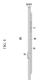
- FIG. 1 is a side view of a chip on film according to a first embodiment.
- FIG. 2 is a base view of the chip on film according to the first embodiment.
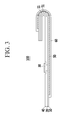
- FIG. 3 is a side view of a state where a bending portion of the chip on film according to the first embodiment is bent.
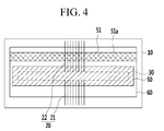
- FIG. 4 is a base view of a chip on film according to a second embodiment.
- FIG. 5 is a side view of a state where a bending portion of the chip on film according to the second embodiment is bent.
- FIG. 6 is a side view of a display device including the chip on film according to the first embodiment.
- FIG. 1 is a side view of a chip on film according to a first embodiment
- FIG. 2 is a base view of the chip on film according to the first embodiment
- FIG. 3 is a side view of a state where a bending portion of the chip on film according to the first embodiment is bent.
- a chip on film 100 includes a driving film 10, a wire layer 20 formed on the driving film 10, a driving chip 30 connected to the wire layer 20, a cover layer 40 covering the wire layer 20, an electromagnetic wave blocking layer 50 formed under the driving film 10, and an insulation layer 60 covering the electromagnetic wave blocking layer 50.
- the wire layer 20 is formed on a first surface of the driving film 10 while the electromagnetic wave blocking layer 50 is formed on a second surface of the driving film 10.
- the driving film 10 may be a flexible film including polyimide and the like.
- the wire layer 20 includes a plurality of signal transferring lines 21 and 22 transferring a driving signal to the driving chip 30 that acts as an interface between a flexible printed circuit (FPC) and a display substrate.
- the plurality of signal transferring lines includes an input signal transferring line 21 inputting a driving signal to the driving chip 30 and an output signal transferring line 22 outputting the driving signal from the driving chip 30.
- the input signal transferring line 21 includes a high-speed data transferring wire, that affects electromagnetic interference (EMI), and the output signal transferring line 22 includes a source output wire, that affects electromagnetic susceptibility (EMS).
- EMI electromagnetic interference
- EMS electromagnetic susceptibility
- the electromagnetic wave blocking layer 50 blocks discharging of an electromagnetic wave occurring from the wire layer 20 to the outside, and the electromagnetic wave blocking layer 50 covers an entire surface under the driving film 10.
- the electromagnetic wave blocking layer 50 may be formed of a metal-plated layer to form a thin film, and the metal-plated layer may include electromagnetic wave blocking metal such as a copper-plated layer and may be formed of the same metal as the wire layer 20.
- the electromagnetic wave blocking layer 50 may block the electromagnetic wave occurring in the wire layer 20 formed on the driving film 10, and particularly in the high-speed data transferring wire 21 through impedance matching to minimize the electromagnetic interference (EMI) occurring in the display device to which the chip on film 100 is connected.
- EMI electromagnetic interference
- the flexible driving film 10 (or the chip on film 100) has a bendable bending portion 11, and a mesh portion 51 is formed on the electromagnetic wave blocking layer 50 at a position corresponding to the bending portion 11.
- the mesh portion 51 is a portion where a mesh pattern 51a is formed on the electromagnetic wave blocking layer 50, and the mesh pattern 51a is formed by removing two diagonal layers 5 crossing each other from the electromagnetic wave blocking layer 50.
- the entire electromagnetic wave blocking layer 50 covers the entire surface under the driving film 10
- FIG. 4 is a base view of a chip on film according to the second embodiment.
- the second embodiment illustrated in FIGS. 4 and 5 is substantially the same as the first embodiment illustrated in FIGS. 1 to 3 , with the exception of the configuration of the electromagnetic wave blocking layer, and a repeated description will be omitted.
- the chip on film according to the second embodiment includes a driving film 10, a wire layer 20 formed on the driving film 10, a driving chip 30 connected to the wire layer 20, a cover layer 40 covering the wire layer 20, an electromagnetic wave blocking layer 50 with a part which blocks electromagnetic waves formed under the driving film 10, and an insulation layer 60 covering the electromagnetic wave blocking layer 50.
- the part of the electromagnetic wave blocking layer which blocks electromagnetic waves 50 covers the position corresponding to the driving chip 30 under the driving film 10, and may further cover the high-speed data transferring wire 21.
- the mesh portion 51 having the mesh pattern 51a may be formed at a position corresponding to the bending portion 11 of the driving film 10, while being spaced apart from the part of the electromagnetic wave blocking layer 50 that blocks electromagnetic waves between the driving film 10 and the insulation layer 60.
- the electromagnetic wave blocking layer 50 may block the electromagnetic wave occurring in the high-speed data transferring wire 21 through impedance matching to minimize the electromagnetic interference (EMI) occurring in the display device to which the chip on film 100 is connected.
- EMI electromagnetic interference
- FIG. 6 is a side view of a display device including the chip on film according to the first embodiment.
- the display device including the chip on film according to the first embodiment includes the display substrate 200, the chip on film 100 connected to a periphery portion of the display substrate 200, and a flexible printed circuit (FPC) 300 connected to the chip on film 100.
- FPC flexible printed circuit
- the display substrate 200 may be a flexible substrate, and a sealing substrate 400 that is disposed to face the display substrate 200 for sealing and attached to the substrate by a sealant such as epoxy is formed on the display substrate 200.
- the FPC 300 is connected through an anisotropic conductive film (ACF) to the chip on film 100. Accordingly, if a control signal and a data signal are provided from the outside through the FPC 300 to the driving chip 30 of the chip on film 100, the driving chip 30 generates a scan signal and a data signal, and the driving chip 30 transfers the generated signals through the scan line and the data line to the light emitting element of the display substrate 200.
- ACF anisotropic conductive film
- the chip on film 100 includes the driving film 10, the wire layer 20 formed on the driving film 10, the driving chip 30 connected to the wire layer 20, the cover layer 40 covering the wire layer 20, the electromagnetic wave blocking layer 50 formed under the driving film 10, and the insulation layer 60 covering the electromagnetic wave blocking layer 50.
- the electromagnetic wave blocking layer 50 blocks discharging of an electromagnetic wave occurring from the wire layer 20 to the outside, and the electromagnetic wave blocking layer 50 covers an entire surface under the driving film 10.
- the electromagnetic wave blocking layer 50 may be formed by the metal-plated layer to form a thin film, and the metal-plated layer may include electromagnetic wave blocking metal such as the copper-plated layer.
- the electromagnetic wave blocking layer 50 may block the electromagnetic wave occurring in the wire layer 20 formed on the driving film 10, and particularly in the high-speed data transferring wire through impedance matching to minimize the electromagnetic interference (EMI) occurring in the display device to which the chip on film is connected.
- EMI electromagnetic interference
- the flexible driving film 10 has the bendable bending portion 11, and the mesh portion 51 is formed between the driving film 10 and the insulation layer 60 at a position corresponding to the bending portion 11.
- the chip on film is bent at the bending portion 11 to be positioned under the display substrate 200.
- the thickness of the flexible display device may be reduced.
Landscapes
- Engineering & Computer Science (AREA)
- Microelectronics & Electronic Packaging (AREA)
- Physics & Mathematics (AREA)
- Electromagnetism (AREA)
- Nonlinear Science (AREA)
- Mathematical Physics (AREA)
- Chemical & Material Sciences (AREA)
- Crystallography & Structural Chemistry (AREA)
- General Physics & Mathematics (AREA)
- Optics & Photonics (AREA)
- Shielding Devices Or Components To Electric Or Magnetic Fields (AREA)
- Devices For Indicating Variable Information By Combining Individual Elements (AREA)
Abstract
Description
- The described technology relates generally to a chip on film and a display device including the same.
- A display device includes a liquid crystal display (LCD), an organic light emitting diode (OLED) display, and the like, and particularly the OLED display includes a display substrate providing a pixel region and a non-pixel region, and a sealing substrate that is disposed to face the display substrate for encapsulation and attached to the substrate by a sealant such as epoxy. A plurality of light emitting elements connected in a matrix manner between a scan line and a data line to constitute a pixel is formed in the pixel region of the display substrate, and a scan driver and a data driver extending from the scan line and the data line of the pixel region and processing a signal provided from the outside through a pad to provide the processed signal to the scan line and the data line are formed in the non-pixel region. The scan driver and the data driver include a driving circuit processing the signal provided from the outside to generate a scan signal and a data signal, and are formed in the course of manufacturing the light emitting element or manufactured as a separate integrated circuit chip form to be mounted on the display substrate.
- In the case where the scan driver and the data driver are manufactured in an integrated circuit chip form to be mounted on the display substrate, a drive IC may be mounted on a chip on film (COF) to be connected to the pad of the display substrate. A wire layer formed on the COF includes a RGB interface wire and the like, the aforementioned wire layer does not cause electromagnetic hindrances such as electromagnetic interference (EMI), but a wire layer of the COF applied to a flexible display device having high resolution includes wires for transferring high-speed data, for example, mobile industry processor interface (MIPI) wires, source output wires, and the like, causing electromagnetic hindrances such as electromagnetic interference (EMI).
- Further, since the wire layer of the COF applied to the flexible display device of the thin film is formed of a single layer in order to form a thin chip on film, it is difficult to adjust an impedance matching level between the display substrate and the chip on film, and thus, it is difficult to remove noise by electromagnetic interference (EMI).
- Further, in the case where an electromagnetic interference prevention tape adheres to the chip on film in order to block the electromagnetic wave, the thickness of the flexible display device is increased.
- The above information disclosed in this Background section is only for enhancement of understanding of the background of the described technology and therefore it may contain information that does not form the prior art that is already known in this country to a person of ordinary skill in the art.
- The described technology has been made in an effort to provide a chip on film of a thin film, which can block an electromagnetic interference, and a display device including the same.
- In a first aspect, the present invention provides a chip on film including: a driving film, a wire layer formed on a first surface of the driving film, a driving chip connected to the wire layer, an electromagnetic wave blocking layer formed on a second surface of the driving film wherein at least a part of said electromagnetic wave blocking layer (50) is configured to block electromagnetic waves, and a mesh portion formed on the second surface of the driving film.
- The mesh portion may be formed on a bending portion of the driving film.
- The mesh portion may be a portion where a mesh pattern is formed on the electromagnetic wave blocking layer.
- The electromagnetic wave blocking layer may be a metal-plated layer.
- The chip on film may further include: an insulation layer covering the electromagnetic wave blocking layer.
- The chip on film may further include: a cover layer covering the wire layer.
- The electromagnetic wave blocking layer may cover an entire surface under the driving film.
- The electromagnetic wave blocking layer may cover a position corresponding to the driving chip under the driving film.
- The mesh portion may b spaced apart from said part of the electromagnetic wave blocking layer configured to block electromagnetic waves.
- In a further aspect, the present invention provides a display device including: a display substrate, a chip on film connected to a periphery portion of the display substrate, and a flexible printed circuit (FPC) connected to the chip on film, in which the chip on film may include a driving film, a wire layer formed on a first surface of the driving film, a driving chip connected to the wire layer, and an electromagnetic wave blocking layer formed on a second surface of the driving film wherein at least a part of said electromagnetic wave blocking layer (50) is configured to block electromagnetic waves, and a mesh portion may be formed on a portion of the electromagnetic wave blocking layer.
- The display substrate may be a flexible substrate.
- The driving chip may be positioned under the display substrate.
- The mesh portion may be formed at a position corresponding to a bending portion of the driving film.
- The electromagnetic wave blocking layer may be a metal-plated layer.
- The mesh portion may be a portion where a mesh pattern is formed on the metal-plated layer.
- The display device may further include: an insulation layer covering the electromagnetic wave blocking layer.
- The display device may further include: a cover layer covering the wire layer.
- The part of said electromagnetic wave blocking layer configured to block electromagnetic waves may cover an entire surface under the driving film, or it may cover a position corresponding to the driving chip under the driving film.
- In a chip on film according to the embodiments, it is possible to minimize electromagnetic interference (EMI) in a display device to which the chip on film is connected by forming an electromagnetic wave blocking layer under a driving film by a metal-plated layer to block an electromagnetic wave occurring in a wire layer formed on the driving film, particularly a high-speed data transferring wire.
- Further, it is possible to alleviate tension of a bending portion and improve electromagnetic susceptibility (EMS) by forming a mesh portion on the electromagnetic wave blocking layer at a position corresponding to the bending portion of the driving film.
-
FIG. 1 is a side view of a chip on film according to a first embodiment. -
FIG. 2 is a base view of the chip on film according to the first embodiment. -
FIG. 3 is a side view of a state where a bending portion of the chip on film according to the first embodiment is bent. -
FIG. 4 is a base view of a chip on film according to a second embodiment. -
FIG. 5 is a side view of a state where a bending portion of the chip on film according to the second embodiment is bent. -
FIG. 6 is a side view of a display device including the chip on film according to the first embodiment. - The present invention will be described more fully hereinafter with reference to the accompanying drawings, in which embodiments of the invention are shown. As those skilled in the art would realize, the described embodiments may be modified in various different ways, all without departing from the scope of the present invention as defined by the appended claims.
- The drawings and description are to be regarded as illustrative in nature and not restrictive. Like reference numerals designate like elements throughout the specification. The size and thickness of each configuration shown in the drawings are arbitrarily shown for understanding and ease of description, but the present invention is not limited thereto.
- Throughout the specification, it will be understood that when an element such as a layer, film, region, or substrate is referred to as being "on" another element, it can be directly on the other element or intervening elements may also be present.
-
FIG. 1 is a side view of a chip on film according to a first embodiment,FIG. 2 is a base view of the chip on film according to the first embodiment, andFIG. 3 is a side view of a state where a bending portion of the chip on film according to the first embodiment is bent. - As shown in
FIG. 1 , a chip onfilm 100 according to the first embodiment includes adriving film 10, awire layer 20 formed on thedriving film 10, a drivingchip 30 connected to thewire layer 20, acover layer 40 covering thewire layer 20, an electromagneticwave blocking layer 50 formed under thedriving film 10, and aninsulation layer 60 covering the electromagneticwave blocking layer 50. In other words, thewire layer 20 is formed on a first surface of thedriving film 10 while the electromagneticwave blocking layer 50 is formed on a second surface of thedriving film 10. - The
driving film 10 may be a flexible film including polyimide and the like. - The
wire layer 20 includes a plurality ofsignal transferring lines chip 30 that acts as an interface between a flexible printed circuit (FPC) and a display substrate. The plurality of signal transferring lines includes an inputsignal transferring line 21 inputting a driving signal to thedriving chip 30 and an outputsignal transferring line 22 outputting the driving signal from thedriving chip 30. - The input
signal transferring line 21 includes a high-speed data transferring wire, that affects electromagnetic interference (EMI), and the outputsignal transferring line 22 includes a source output wire, that affects electromagnetic susceptibility (EMS). - The electromagnetic
wave blocking layer 50 blocks discharging of an electromagnetic wave occurring from thewire layer 20 to the outside, and the electromagneticwave blocking layer 50 covers an entire surface under thedriving film 10. The electromagneticwave blocking layer 50 may be formed of a metal-plated layer to form a thin film, and the metal-plated layer may include electromagnetic wave blocking metal such as a copper-plated layer and may be formed of the same metal as thewire layer 20. - Accordingly, the electromagnetic
wave blocking layer 50 may block the electromagnetic wave occurring in thewire layer 20 formed on thedriving film 10, and particularly in the high-speeddata transferring wire 21 through impedance matching to minimize the electromagnetic interference (EMI) occurring in the display device to which the chip onfilm 100 is connected. - As shown in
FIGS. 2 and3 , the flexible driving film 10 (or the chip on film 100) has abendable bending portion 11, and amesh portion 51 is formed on the electromagneticwave blocking layer 50 at a position corresponding to thebending portion 11. Themesh portion 51 is a portion where amesh pattern 51a is formed on the electromagneticwave blocking layer 50, and themesh pattern 51a is formed by removing twodiagonal layers 5 crossing each other from the electromagneticwave blocking layer 50. - As described above, it is possible to improve the electromagnetic susceptibility (EMS) and alleviate tension of the
bending portion 11 by forming the electromagneticwave blocking layer 50 at a position corresponding to thebending portion 11 of thedriving film 10 and forming themesh portion 51 on the electromagneticwave blocking layer 50 at the position corresponding to thebending portion 11 of thedriving film 10. - Meanwhile, in the first embodiment, the entire electromagnetic
wave blocking layer 50 covers the entire surface under thedriving film 10, but a second embodiment where electromagneticwave blocking layer 50 only a part of the electromagnetic wave blocking layer is configured to block electromagnetic waves, and this part of the layer covers only the position corresponding to thedriving chip 30 under the driving film. - Hereinafter, the second embodiment will be described in detail with reference to
FIGS. 4 and5 . -
FIG. 4 is a base view of a chip on film according to the second embodiment. - The second embodiment illustrated in
FIGS. 4 and5 is substantially the same as the first embodiment illustrated inFIGS. 1 to 3 , with the exception of the configuration of the electromagnetic wave blocking layer, and a repeated description will be omitted. - As shown in
FIGS. 4 and5 , the chip on film according to the second embodiment includes adriving film 10, awire layer 20 formed on thedriving film 10, a drivingchip 30 connected to thewire layer 20, acover layer 40 covering thewire layer 20, an electromagneticwave blocking layer 50 with a part which blocks electromagnetic waves formed under thedriving film 10, and aninsulation layer 60 covering the electromagneticwave blocking layer 50. - The part of the electromagnetic wave blocking layer which blocks
electromagnetic waves 50 covers the position corresponding to thedriving chip 30 under the drivingfilm 10, and may further cover the high-speeddata transferring wire 21. Themesh portion 51 having themesh pattern 51a may be formed at a position corresponding to the bendingportion 11 of the drivingfilm 10, while being spaced apart from the part of the electromagneticwave blocking layer 50 that blocks electromagnetic waves between the drivingfilm 10 and theinsulation layer 60. - Accordingly, the electromagnetic
wave blocking layer 50 may block the electromagnetic wave occurring in the high-speeddata transferring wire 21 through impedance matching to minimize the electromagnetic interference (EMI) occurring in the display device to which the chip onfilm 100 is connected. - Meanwhile, hereinafter, the display device including the chip on film according to the first embodiment will be described in detail.
-
FIG. 6 is a side view of a display device including the chip on film according to the first embodiment. - As shown in
FIG. 6 , the display device including the chip on film according to the first embodiment includes thedisplay substrate 200, the chip onfilm 100 connected to a periphery portion of thedisplay substrate 200, and a flexible printed circuit (FPC) 300 connected to the chip onfilm 100. - The
display substrate 200 may be a flexible substrate, and a sealingsubstrate 400 that is disposed to face thedisplay substrate 200 for sealing and attached to the substrate by a sealant such as epoxy is formed on thedisplay substrate 200. - The
FPC 300 is connected through an anisotropic conductive film (ACF) to the chip onfilm 100. Accordingly, if a control signal and a data signal are provided from the outside through theFPC 300 to thedriving chip 30 of the chip onfilm 100, thedriving chip 30 generates a scan signal and a data signal, and thedriving chip 30 transfers the generated signals through the scan line and the data line to the light emitting element of thedisplay substrate 200. - The chip on
film 100 includes the drivingfilm 10, thewire layer 20 formed on the drivingfilm 10, thedriving chip 30 connected to thewire layer 20, thecover layer 40 covering thewire layer 20, the electromagneticwave blocking layer 50 formed under the drivingfilm 10, and theinsulation layer 60 covering the electromagneticwave blocking layer 50. - The electromagnetic
wave blocking layer 50 blocks discharging of an electromagnetic wave occurring from thewire layer 20 to the outside, and the electromagneticwave blocking layer 50 covers an entire surface under the drivingfilm 10. The electromagneticwave blocking layer 50 may be formed by the metal-plated layer to form a thin film, and the metal-plated layer may include electromagnetic wave blocking metal such as the copper-plated layer. - Accordingly, the electromagnetic
wave blocking layer 50 may block the electromagnetic wave occurring in thewire layer 20 formed on the drivingfilm 10, and particularly in the high-speed data transferring wire through impedance matching to minimize the electromagnetic interference (EMI) occurring in the display device to which the chip on film is connected. - Further, the
flexible driving film 10 has thebendable bending portion 11, and themesh portion 51 is formed between the drivingfilm 10 and theinsulation layer 60 at a position corresponding to the bendingportion 11. The chip on film is bent at the bendingportion 11 to be positioned under thedisplay substrate 200. - As described above, it is possible to improve the electromagnetic susceptibility (EMS) and alleviate tension of the bending
portion 11 by forming the electromagneticwave blocking layer 50 at a position corresponding to the bendingportion 11 of the drivingfilm 10 and forming themesh portion 51 on the electromagneticwave blocking layer 50 at the position corresponding to the bendingportion 11 of the drivingfilm 10, thus maximizing a bending angle of the bendingportion 11 to minimize the thickness of the bent chip on film. Therefore, the thickness of the flexible display device may be reduced. - While this disclosure has been described in connection with what is presently considered to be practical embodiments, it is to be understood that the invention is not limited to the disclosed embodiments, but, on the contrary, is intended to cover various modifications and equivalent arrangements included within the scope of the present invention as defined by the appended claims.
Claims (12)
- A chip on film (100) comprising:a driving film (10),a wire layer (20) formed on a first surface of the driving film (10),a driving chip (30) connected to the wire layer (20),an electromagnetic wave blocking layer (50) formed on a second surface of the driving film (10) wherein at least a part of said electromagnetic wave blocking layer (50) is configured to block electromagnetic waves; anda mesh portion (51) is formed on the second surface of the driving film (10).
- The chip on film of claim 1, wherein the mesh portion (51) is formed on a bending portion (11) of the driving film (10).
- The chip on film according to any preceding claim, wherein the mesh portion (51) is a portion where a mesh pattern (51a) is formed on the electromagnetic wave blocking layer (50).
- The chip on film according to any precedng claim, wherein the at least a part of said electromagnetic wave blocking layer (50) configured to block electromagnetic waves is metal-plated..
- The chip on film according to any preceding claim, further comprising an insulation layer (60) covering the electromagnetic wave blocking layer (50).
- The chip on film according to any preceding claim, further comprising a cover layer (40) covering the wire layer (20).
- The chip on film according to any preceding claim, wherein the at least a part of said electromagnetic wave blocking layer (50) configured to block electromagnetic waves covers an entire surface under the driving film (10).
- The chip on film according to any of claims 1 to 6, wherein said part of the electromagnetic wave blocking layer (50) configured to block electromagnetic waves covers a position corresponding to the driving chip (30) under the driving film (10).
- The chip on film according to claim 8, wherein the mesh portion (51) is spaced apart from said part of the electromagnetic wave blocking layer (50) configured to block electromagnetic waves.
- A display device comprising:a display substrate (200),a chip on film (100) connected to a periphery portion of the display substrate (200),
anda flexible printed circuit (FPC) (300) connected to the chip on film (100), wherein the chip on film is a chip on film (100) as recited in any preceding claim. - The display device of claim 10, wherein the display substrate (200) is a flexible substrate.
- The display device of claim 10, wherein the driving chip (30) is positioned under the display substrate (200).
Applications Claiming Priority (1)
| Application Number | Priority Date | Filing Date | Title |
|---|---|---|---|
| KR1020120119149A KR101979361B1 (en) | 2012-10-25 | 2012-10-25 | Chip on film and display device including the same |
Publications (2)
| Publication Number | Publication Date |
|---|---|
| EP2725881A1 true EP2725881A1 (en) | 2014-04-30 |
| EP2725881B1 EP2725881B1 (en) | 2015-06-24 |
Family
ID=49554002
Family Applications (1)
| Application Number | Title | Priority Date | Filing Date |
|---|---|---|---|
| EP13190371.8A Active EP2725881B1 (en) | 2012-10-25 | 2013-10-25 | Chip on film and display device including the same |
Country Status (3)
| Country | Link |
|---|---|
| US (1) | US20140118969A1 (en) |
| EP (1) | EP2725881B1 (en) |
| KR (1) | KR101979361B1 (en) |
Cited By (7)
| Publication number | Priority date | Publication date | Assignee | Title |
|---|---|---|---|---|
| CN106486520A (en) * | 2015-08-24 | 2017-03-08 | 三星显示有限公司 | Flexible display and its manufacture method |
| CN107948363A (en) * | 2016-11-16 | 2018-04-20 | 广东欧珀移动通信有限公司 | A camera installation structure of a mobile terminal and the mobile terminal |
| WO2019040514A1 (en) * | 2017-08-21 | 2019-02-28 | The Charles Stark Draper Laboratory, Inc. | Multi-layered fabrication processing |
| WO2019085276A1 (en) * | 2017-10-30 | 2019-05-09 | 武汉华星光电半导体显示技术有限公司 | Bending device and bending method for gate driving region |
| WO2019112836A1 (en) * | 2017-12-05 | 2019-06-13 | Google Llc | Shielding a bending portion of a flexible display |
| EP3588569A1 (en) * | 2018-06-22 | 2020-01-01 | Samsung Display Co., Ltd. | Flexible substrate and display device including the same |
| EP3876684A1 (en) * | 2020-03-04 | 2021-09-08 | Samsung Display Co., Ltd. | Display device |
Families Citing this family (21)
| Publication number | Priority date | Publication date | Assignee | Title |
|---|---|---|---|---|
| US9379355B1 (en) | 2014-12-15 | 2016-06-28 | Lg Display Co., Ltd. | Flexible display device having support layer with rounded edge |
| JP6406453B2 (en) * | 2015-07-01 | 2018-10-17 | 株式会社村田製作所 | Resin substrate, resin substrate manufacturing method |
| CN106358360B (en) | 2015-07-14 | 2019-07-19 | 财团法人工业技术研究院 | Flexible electronic device and method of making the same |
| JP6426067B2 (en) * | 2015-08-06 | 2018-11-21 | 日本メクトロン株式会社 | Multilayer flexible printed wiring board and method of manufacturing the same |
| KR102257253B1 (en) * | 2015-10-06 | 2021-05-28 | 엘지이노텍 주식회사 | Flexible Substrate |
| US9978674B2 (en) | 2016-04-05 | 2018-05-22 | Samsung Electronics Co., Ltd. | Chip-on-film semiconductor packages and display apparatus including the same |
| KR102532627B1 (en) * | 2016-06-10 | 2023-05-15 | 삼성디스플레이 주식회사 | Cof package and display device comprising the same |
| KR102556022B1 (en) * | 2016-07-06 | 2023-07-17 | 삼성디스플레이 주식회사 | Flexible display device |
| KR102631839B1 (en) * | 2016-09-07 | 2024-01-31 | 삼성디스플레이 주식회사 | Display device |
| CN107004392B (en) * | 2016-11-28 | 2019-11-05 | 上海云英谷科技有限公司 | The distributed driving of display panel |
| JP2018116137A (en) * | 2017-01-18 | 2018-07-26 | 株式会社ジャパンディスプレイ | Display and method for manufacturing the same |
| US10468470B2 (en) * | 2017-02-27 | 2019-11-05 | Wuhan China Star Optoelectronics Technology Co., Ltd | OLED display module and method of forming the same |
| CN108574158B (en) * | 2017-03-14 | 2020-10-09 | 群创光电股份有限公司 | Display device and method for manufacturing the same |
| KR102543688B1 (en) * | 2018-04-02 | 2023-06-14 | 삼성디스플레이 주식회사 | Display device and manufacturing method of display device |
| JP2020030298A (en) * | 2018-08-22 | 2020-02-27 | 株式会社ジャパンディスプレイ | Display device and integrated circuit module |
| CN109559640A (en) * | 2018-12-05 | 2019-04-02 | 京东方科技集团股份有限公司 | A kind of display module and preparation method thereof and display device |
| CN112639929A (en) * | 2018-12-29 | 2021-04-09 | 深圳市柔宇科技股份有限公司 | Display device |
| KR102763671B1 (en) * | 2019-05-02 | 2025-02-06 | 삼성디스플레이 주식회사 | Dispcay device |
| CN113039593B (en) | 2019-08-28 | 2022-11-25 | 京东方科技集团股份有限公司 | Display panel, display module, manufacturing method of display module and communication device |
| KR20210060733A (en) * | 2019-11-18 | 2021-05-27 | 삼성디스플레이 주식회사 | Display apparatus |
| CN114793383B (en) * | 2021-01-25 | 2025-02-18 | 北京京东方光电科技有限公司 | A flexible circuit board and its manufacturing method, and a display device |
Citations (4)
| Publication number | Priority date | Publication date | Assignee | Title |
|---|---|---|---|---|
| US5917149A (en) * | 1997-05-15 | 1999-06-29 | Daimlerchrysler Corporation | Flexible circuit board interconnect with strain relief |
| US20070013056A1 (en) * | 2005-07-18 | 2007-01-18 | Samsung Electronics Co., Ltd. | Tape wiring substrate and chip-on-film package using the same |
| US20070134473A1 (en) * | 2005-12-12 | 2007-06-14 | Ock-Jin Kim | Flexible circuit film and display panel assembly having the same |
| US20100290192A1 (en) * | 2008-01-17 | 2010-11-18 | Tatsuya Katoh | Semiconductor device and display apparatus |
Family Cites Families (13)
| Publication number | Priority date | Publication date | Assignee | Title |
|---|---|---|---|---|
| KR101008973B1 (en) * | 2003-10-11 | 2011-01-17 | 삼성전자주식회사 | Tape wiring board, semiconductor chip package using the same, and liquid crystal display using the same |
| JP3722223B2 (en) * | 2003-10-27 | 2005-11-30 | セイコーエプソン株式会社 | Semiconductor device and manufacturing method thereof, electronic module, and electronic apparatus |
| CN101222815A (en) * | 2006-12-15 | 2008-07-16 | 富葵精密组件(深圳)有限公司 | Flexible Printed Circuit Board |
| KR101535223B1 (en) * | 2008-08-18 | 2015-07-09 | 삼성전자주식회사 | Tape circuit boards, chip-on-film packages and device assemblies |
| JP4605272B2 (en) * | 2008-08-22 | 2011-01-05 | 住友金属鉱山株式会社 | COF substrate |
| KR101155907B1 (en) * | 2009-06-04 | 2012-06-20 | 삼성모바일디스플레이주식회사 | Organic light emitting diode display and method for manufacturing the same |
| TWI476738B (en) * | 2010-09-07 | 2015-03-11 | Ind Tech Res Inst | Flexible display panel and assembly method thereof |
| KR101521114B1 (en) * | 2010-12-03 | 2015-05-19 | 엘지디스플레이 주식회사 | Organic Light Emitting Display Device And Method For Manufacturing The Same |
| KR101855245B1 (en) * | 2011-07-13 | 2018-05-08 | 삼성전자 주식회사 | Touch screen panel active matrix organic light emitting diode display device |
| KR101838736B1 (en) * | 2011-12-20 | 2018-03-15 | 삼성전자 주식회사 | Tape wiring substrate and chip on film package including the same |
| KR101633373B1 (en) * | 2012-01-09 | 2016-06-24 | 삼성전자 주식회사 | COF package and semiconductor comprising the same |
| US9521748B1 (en) * | 2013-12-09 | 2016-12-13 | Multek Technologies, Ltd. | Mechanical measures to limit stress and strain in deformable electronics |
| US9706607B2 (en) * | 2014-12-10 | 2017-07-11 | Lg Display Co., Ltd. | Flexible display device with multiple types of micro-coating layers |
-
2012
- 2012-10-25 KR KR1020120119149A patent/KR101979361B1/en not_active Expired - Fee Related
-
2013
- 2013-10-24 US US14/062,678 patent/US20140118969A1/en not_active Abandoned
- 2013-10-25 EP EP13190371.8A patent/EP2725881B1/en active Active
Patent Citations (4)
| Publication number | Priority date | Publication date | Assignee | Title |
|---|---|---|---|---|
| US5917149A (en) * | 1997-05-15 | 1999-06-29 | Daimlerchrysler Corporation | Flexible circuit board interconnect with strain relief |
| US20070013056A1 (en) * | 2005-07-18 | 2007-01-18 | Samsung Electronics Co., Ltd. | Tape wiring substrate and chip-on-film package using the same |
| US20070134473A1 (en) * | 2005-12-12 | 2007-06-14 | Ock-Jin Kim | Flexible circuit film and display panel assembly having the same |
| US20100290192A1 (en) * | 2008-01-17 | 2010-11-18 | Tatsuya Katoh | Semiconductor device and display apparatus |
Cited By (18)
| Publication number | Priority date | Publication date | Assignee | Title |
|---|---|---|---|---|
| CN106486520A (en) * | 2015-08-24 | 2017-03-08 | 三星显示有限公司 | Flexible display and its manufacture method |
| CN106486520B (en) * | 2015-08-24 | 2023-01-31 | 三星显示有限公司 | Flexible display and manufacturing method thereof |
| CN107948363A (en) * | 2016-11-16 | 2018-04-20 | 广东欧珀移动通信有限公司 | A camera installation structure of a mobile terminal and the mobile terminal |
| WO2019040514A1 (en) * | 2017-08-21 | 2019-02-28 | The Charles Stark Draper Laboratory, Inc. | Multi-layered fabrication processing |
| WO2019085276A1 (en) * | 2017-10-30 | 2019-05-09 | 武汉华星光电半导体显示技术有限公司 | Bending device and bending method for gate driving region |
| US10952356B2 (en) | 2017-12-05 | 2021-03-16 | Google Llc | Shielding portions of an electronic device |
| CN110692029A (en) * | 2017-12-05 | 2020-01-14 | 谷歌有限责任公司 | Curved portion of shielded flexible display |
| US10602645B2 (en) | 2017-12-05 | 2020-03-24 | Google Llc | Shielding portions of an electronic device |
| WO2019112836A1 (en) * | 2017-12-05 | 2019-06-13 | Google Llc | Shielding a bending portion of a flexible display |
| CN110692029B (en) * | 2017-12-05 | 2024-02-06 | 谷歌有限责任公司 | Shielding curved portions of a flexible display |
| EP4482130A3 (en) * | 2017-12-05 | 2025-02-26 | Google Llc | Shielding a bending portion of a flexible display |
| EP3588569A1 (en) * | 2018-06-22 | 2020-01-01 | Samsung Display Co., Ltd. | Flexible substrate and display device including the same |
| US11013108B2 (en) | 2018-06-22 | 2021-05-18 | Samsung Display Co., Ltd. | Flexible substrate with bubble-prevention layer and display device including the same |
| US11425813B2 (en) | 2018-06-22 | 2022-08-23 | Samsung Display Co., Ltd. | Display device including flexible substrate with bubble-prevention layer |
| EP3876684A1 (en) * | 2020-03-04 | 2021-09-08 | Samsung Display Co., Ltd. | Display device |
| US11520384B2 (en) | 2020-03-04 | 2022-12-06 | Samsung Display Co., Ltd. | Display device |
| US11714466B2 (en) | 2020-03-04 | 2023-08-01 | Samsung Display Co., Ltd. | Display device |
| US12007817B2 (en) | 2020-03-04 | 2024-06-11 | Samsung Display Co., Ltd. | Display device |
Also Published As
| Publication number | Publication date |
|---|---|
| US20140118969A1 (en) | 2014-05-01 |
| KR20140052708A (en) | 2014-05-07 |
| KR101979361B1 (en) | 2019-05-17 |
| EP2725881B1 (en) | 2015-06-24 |
Similar Documents
| Publication | Publication Date | Title |
|---|---|---|
| EP2725881B1 (en) | Chip on film and display device including the same | |
| CN111933611B (en) | A display panel and a display device | |
| US10910410B2 (en) | Flexible array substrate, flexible display device and method of assembling the same | |
| CN107170366B (en) | Display panel and display device | |
| JP5508680B2 (en) | Display device | |
| KR102330882B1 (en) | Display device | |
| CN109459895A (en) | Display panel and display device | |
| EP3901696B1 (en) | Display device | |
| TWI504969B (en) | Display panel and display device | |
| KR102777809B1 (en) | Flexible display apparatus and electronic device comprising the same | |
| JP2013167694A (en) | Display device | |
| US8922542B2 (en) | Chip-on-film package and display device having the same | |
| KR102215881B1 (en) | Tape package and display apparatus having the same | |
| US10204926B2 (en) | Display device and display panel | |
| US11251256B2 (en) | Display apparatus | |
| CN111885821A (en) | Display device and printed circuit board with anisotropic conductive film | |
| KR102314774B1 (en) | Semiconductor package | |
| KR102703342B1 (en) | Antenna package and image display device including the same | |
| CN102981326A (en) | fan-out circuit | |
| KR102035006B1 (en) | flexible printed circuit and display device | |
| JP2009186777A (en) | Liquid crystal display | |
| CN109979978B (en) | Display devices, display panels and circuit boards | |
| US20170263689A1 (en) | Display device | |
| KR20190079086A (en) | Flexible display device | |
| US10739891B2 (en) | Touch display device |
Legal Events
| Date | Code | Title | Description |
|---|---|---|---|
| PUAI | Public reference made under article 153(3) epc to a published international application that has entered the european phase |
Free format text: ORIGINAL CODE: 0009012 |
|
| 17P | Request for examination filed |
Effective date: 20131025 |
|
| AK | Designated contracting states |
Kind code of ref document: A1 Designated state(s): AL AT BE BG CH CY CZ DE DK EE ES FI FR GB GR HR HU IE IS IT LI LT LU LV MC MK MT NL NO PL PT RO RS SE SI SK SM TR |
|
| AX | Request for extension of the european patent |
Extension state: BA ME |
|
| 17P | Request for examination filed |
Effective date: 20140328 |
|
| RBV | Designated contracting states (corrected) |
Designated state(s): AL AT BE BG CH CY CZ DE DK EE ES FI FR GB GR HR HU IE IS IT LI LT LU LV MC MK MT NL NO PL PT RO RS SE SI SK SM TR |
|
| GRAP | Despatch of communication of intention to grant a patent |
Free format text: ORIGINAL CODE: EPIDOSNIGR1 |
|
| RIC1 | Information provided on ipc code assigned before grant |
Ipc: H01L 23/552 20060101ALI20141215BHEP Ipc: G02F 1/1345 20060101ALN20141215BHEP Ipc: H05K 1/18 20060101ALN20141215BHEP Ipc: H05K 1/02 20060101AFI20141215BHEP Ipc: H01L 23/498 20060101ALI20141215BHEP |
|
| RIC1 | Information provided on ipc code assigned before grant |
Ipc: H01L 23/498 20060101ALI20141222BHEP Ipc: G02F 1/1345 20060101ALN20141222BHEP Ipc: H05K 1/18 20060101ALN20141222BHEP Ipc: H05K 1/02 20060101AFI20141222BHEP Ipc: H01L 23/552 20060101ALI20141222BHEP |
|
| INTG | Intention to grant announced |
Effective date: 20150114 |
|
| RIN1 | Information on inventor provided before grant (corrected) |
Inventor name: LEE, HEE-KWON |
|
| GRAS | Grant fee paid |
Free format text: ORIGINAL CODE: EPIDOSNIGR3 |
|
| GRAA | (expected) grant |
Free format text: ORIGINAL CODE: 0009210 |
|
| AK | Designated contracting states |
Kind code of ref document: B1 Designated state(s): AL AT BE BG CH CY CZ DE DK EE ES FI FR GB GR HR HU IE IS IT LI LT LU LV MC MK MT NL NO PL PT RO RS SE SI SK SM TR |
|
| REG | Reference to a national code |
Ref country code: GB Ref legal event code: FG4D |
|
| REG | Reference to a national code |
Ref country code: CH Ref legal event code: EP |
|
| REG | Reference to a national code |
Ref country code: AT Ref legal event code: REF Ref document number: 733377 Country of ref document: AT Kind code of ref document: T Effective date: 20150715 |
|
| REG | Reference to a national code |
Ref country code: IE Ref legal event code: FG4D |
|
| REG | Reference to a national code |
Ref country code: DE Ref legal event code: R096 Ref document number: 602013002082 Country of ref document: DE |
|
| RAP2 | Party data changed (patent owner data changed or rights of a patent transferred) |
Owner name: SAMSUNG DISPLAY CO., LTD. |
|
| PG25 | Lapsed in a contracting state [announced via postgrant information from national office to epo] |
Ref country code: NO Free format text: LAPSE BECAUSE OF FAILURE TO SUBMIT A TRANSLATION OF THE DESCRIPTION OR TO PAY THE FEE WITHIN THE PRESCRIBED TIME-LIMIT Effective date: 20150924 Ref country code: LT Free format text: LAPSE BECAUSE OF FAILURE TO SUBMIT A TRANSLATION OF THE DESCRIPTION OR TO PAY THE FEE WITHIN THE PRESCRIBED TIME-LIMIT Effective date: 20150624 Ref country code: HR Free format text: LAPSE BECAUSE OF FAILURE TO SUBMIT A TRANSLATION OF THE DESCRIPTION OR TO PAY THE FEE WITHIN THE PRESCRIBED TIME-LIMIT Effective date: 20150624 Ref country code: FI Free format text: LAPSE BECAUSE OF FAILURE TO SUBMIT A TRANSLATION OF THE DESCRIPTION OR TO PAY THE FEE WITHIN THE PRESCRIBED TIME-LIMIT Effective date: 20150624 |
|
| REG | Reference to a national code |
Ref country code: AT Ref legal event code: MK05 Ref document number: 733377 Country of ref document: AT Kind code of ref document: T Effective date: 20150624 |
|
| REG | Reference to a national code |
Ref country code: LT Ref legal event code: MG4D |
|
| PG25 | Lapsed in a contracting state [announced via postgrant information from national office to epo] |
Ref country code: RS Free format text: LAPSE BECAUSE OF FAILURE TO SUBMIT A TRANSLATION OF THE DESCRIPTION OR TO PAY THE FEE WITHIN THE PRESCRIBED TIME-LIMIT Effective date: 20150624 Ref country code: GR Free format text: LAPSE BECAUSE OF FAILURE TO SUBMIT A TRANSLATION OF THE DESCRIPTION OR TO PAY THE FEE WITHIN THE PRESCRIBED TIME-LIMIT Effective date: 20150925 Ref country code: LV Free format text: LAPSE BECAUSE OF FAILURE TO SUBMIT A TRANSLATION OF THE DESCRIPTION OR TO PAY THE FEE WITHIN THE PRESCRIBED TIME-LIMIT Effective date: 20150624 Ref country code: BG Free format text: LAPSE BECAUSE OF FAILURE TO SUBMIT A TRANSLATION OF THE DESCRIPTION OR TO PAY THE FEE WITHIN THE PRESCRIBED TIME-LIMIT Effective date: 20150924 |
|
| REG | Reference to a national code |
Ref country code: NL Ref legal event code: MP Effective date: 20150624 |
|
| PG25 | Lapsed in a contracting state [announced via postgrant information from national office to epo] |
Ref country code: EE Free format text: LAPSE BECAUSE OF FAILURE TO SUBMIT A TRANSLATION OF THE DESCRIPTION OR TO PAY THE FEE WITHIN THE PRESCRIBED TIME-LIMIT Effective date: 20150624 |
|
| PG25 | Lapsed in a contracting state [announced via postgrant information from national office to epo] |
Ref country code: IS Free format text: LAPSE BECAUSE OF FAILURE TO SUBMIT A TRANSLATION OF THE DESCRIPTION OR TO PAY THE FEE WITHIN THE PRESCRIBED TIME-LIMIT Effective date: 20151024 Ref country code: ES Free format text: LAPSE BECAUSE OF FAILURE TO SUBMIT A TRANSLATION OF THE DESCRIPTION OR TO PAY THE FEE WITHIN THE PRESCRIBED TIME-LIMIT Effective date: 20150624 Ref country code: CZ Free format text: LAPSE BECAUSE OF FAILURE TO SUBMIT A TRANSLATION OF THE DESCRIPTION OR TO PAY THE FEE WITHIN THE PRESCRIBED TIME-LIMIT Effective date: 20150624 Ref country code: AT Free format text: LAPSE BECAUSE OF FAILURE TO SUBMIT A TRANSLATION OF THE DESCRIPTION OR TO PAY THE FEE WITHIN THE PRESCRIBED TIME-LIMIT Effective date: 20150624 Ref country code: SK Free format text: LAPSE BECAUSE OF FAILURE TO SUBMIT A TRANSLATION OF THE DESCRIPTION OR TO PAY THE FEE WITHIN THE PRESCRIBED TIME-LIMIT Effective date: 20150624 Ref country code: RO Free format text: LAPSE BECAUSE OF NON-PAYMENT OF DUE FEES Effective date: 20150624 Ref country code: PL Free format text: LAPSE BECAUSE OF FAILURE TO SUBMIT A TRANSLATION OF THE DESCRIPTION OR TO PAY THE FEE WITHIN THE PRESCRIBED TIME-LIMIT Effective date: 20150624 Ref country code: PT Free format text: LAPSE BECAUSE OF FAILURE TO SUBMIT A TRANSLATION OF THE DESCRIPTION OR TO PAY THE FEE WITHIN THE PRESCRIBED TIME-LIMIT Effective date: 20151026 |
|
| REG | Reference to a national code |
Ref country code: DE Ref legal event code: R097 Ref document number: 602013002082 Country of ref document: DE |
|
| PG25 | Lapsed in a contracting state [announced via postgrant information from national office to epo] |
Ref country code: IT Free format text: LAPSE BECAUSE OF FAILURE TO SUBMIT A TRANSLATION OF THE DESCRIPTION OR TO PAY THE FEE WITHIN THE PRESCRIBED TIME-LIMIT Effective date: 20150624 Ref country code: DK Free format text: LAPSE BECAUSE OF FAILURE TO SUBMIT A TRANSLATION OF THE DESCRIPTION OR TO PAY THE FEE WITHIN THE PRESCRIBED TIME-LIMIT Effective date: 20150624 |
|
| PLBE | No opposition filed within time limit |
Free format text: ORIGINAL CODE: 0009261 |
|
| STAA | Information on the status of an ep patent application or granted ep patent |
Free format text: STATUS: NO OPPOSITION FILED WITHIN TIME LIMIT |
|
| PG25 | Lapsed in a contracting state [announced via postgrant information from national office to epo] |
Ref country code: LU Free format text: LAPSE BECAUSE OF FAILURE TO SUBMIT A TRANSLATION OF THE DESCRIPTION OR TO PAY THE FEE WITHIN THE PRESCRIBED TIME-LIMIT Effective date: 20151025 |
|
| 26N | No opposition filed |
Effective date: 20160329 |
|
| PG25 | Lapsed in a contracting state [announced via postgrant information from national office to epo] |
Ref country code: MC Free format text: LAPSE BECAUSE OF FAILURE TO SUBMIT A TRANSLATION OF THE DESCRIPTION OR TO PAY THE FEE WITHIN THE PRESCRIBED TIME-LIMIT Effective date: 20150624 |
|
| REG | Reference to a national code |
Ref country code: IE Ref legal event code: MM4A |
|
| REG | Reference to a national code |
Ref country code: FR Ref legal event code: ST Effective date: 20160630 |
|
| PG25 | Lapsed in a contracting state [announced via postgrant information from national office to epo] |
Ref country code: FR Free format text: LAPSE BECAUSE OF NON-PAYMENT OF DUE FEES Effective date: 20151102 Ref country code: SI Free format text: LAPSE BECAUSE OF FAILURE TO SUBMIT A TRANSLATION OF THE DESCRIPTION OR TO PAY THE FEE WITHIN THE PRESCRIBED TIME-LIMIT Effective date: 20150624 |
|
| PG25 | Lapsed in a contracting state [announced via postgrant information from national office to epo] |
Ref country code: IE Free format text: LAPSE BECAUSE OF NON-PAYMENT OF DUE FEES Effective date: 20151025 |
|
| PG25 | Lapsed in a contracting state [announced via postgrant information from national office to epo] |
Ref country code: BE Free format text: LAPSE BECAUSE OF FAILURE TO SUBMIT A TRANSLATION OF THE DESCRIPTION OR TO PAY THE FEE WITHIN THE PRESCRIBED TIME-LIMIT Effective date: 20150624 |
|
| PG25 | Lapsed in a contracting state [announced via postgrant information from national office to epo] |
Ref country code: HU Free format text: LAPSE BECAUSE OF FAILURE TO SUBMIT A TRANSLATION OF THE DESCRIPTION OR TO PAY THE FEE WITHIN THE PRESCRIBED TIME-LIMIT; INVALID AB INITIO Effective date: 20131025 |
|
| REG | Reference to a national code |
Ref country code: CH Ref legal event code: PL |
|
| PG25 | Lapsed in a contracting state [announced via postgrant information from national office to epo] |
Ref country code: NL Free format text: LAPSE BECAUSE OF FAILURE TO SUBMIT A TRANSLATION OF THE DESCRIPTION OR TO PAY THE FEE WITHIN THE PRESCRIBED TIME-LIMIT Effective date: 20150624 Ref country code: SE Free format text: LAPSE BECAUSE OF FAILURE TO SUBMIT A TRANSLATION OF THE DESCRIPTION OR TO PAY THE FEE WITHIN THE PRESCRIBED TIME-LIMIT Effective date: 20150624 Ref country code: CY Free format text: LAPSE BECAUSE OF FAILURE TO SUBMIT A TRANSLATION OF THE DESCRIPTION OR TO PAY THE FEE WITHIN THE PRESCRIBED TIME-LIMIT Effective date: 20150624 |
|
| PG25 | Lapsed in a contracting state [announced via postgrant information from national office to epo] |
Ref country code: LI Free format text: LAPSE BECAUSE OF NON-PAYMENT OF DUE FEES Effective date: 20161031 Ref country code: CH Free format text: LAPSE BECAUSE OF NON-PAYMENT OF DUE FEES Effective date: 20161031 |
|
| PG25 | Lapsed in a contracting state [announced via postgrant information from national office to epo] |
Ref country code: MT Free format text: LAPSE BECAUSE OF FAILURE TO SUBMIT A TRANSLATION OF THE DESCRIPTION OR TO PAY THE FEE WITHIN THE PRESCRIBED TIME-LIMIT Effective date: 20150624 |
|
| PG25 | Lapsed in a contracting state [announced via postgrant information from national office to epo] |
Ref country code: SM Free format text: LAPSE BECAUSE OF FAILURE TO SUBMIT A TRANSLATION OF THE DESCRIPTION OR TO PAY THE FEE WITHIN THE PRESCRIBED TIME-LIMIT Effective date: 20150624 |
|
| PG25 | Lapsed in a contracting state [announced via postgrant information from national office to epo] |
Ref country code: MK Free format text: LAPSE BECAUSE OF FAILURE TO SUBMIT A TRANSLATION OF THE DESCRIPTION OR TO PAY THE FEE WITHIN THE PRESCRIBED TIME-LIMIT Effective date: 20150624 |
|
| PG25 | Lapsed in a contracting state [announced via postgrant information from national office to epo] |
Ref country code: TR Free format text: LAPSE BECAUSE OF FAILURE TO SUBMIT A TRANSLATION OF THE DESCRIPTION OR TO PAY THE FEE WITHIN THE PRESCRIBED TIME-LIMIT Effective date: 20150624 Ref country code: AL Free format text: LAPSE BECAUSE OF FAILURE TO SUBMIT A TRANSLATION OF THE DESCRIPTION OR TO PAY THE FEE WITHIN THE PRESCRIBED TIME-LIMIT Effective date: 20150624 |
|
| P01 | Opt-out of the competence of the unified patent court (upc) registered |
Effective date: 20230515 |
|
| PGFP | Annual fee paid to national office [announced via postgrant information from national office to epo] |
Ref country code: GB Payment date: 20240920 Year of fee payment: 12 |
|
| PGFP | Annual fee paid to national office [announced via postgrant information from national office to epo] |
Ref country code: DE Payment date: 20240920 Year of fee payment: 12 |