EP2722868B1 - Oktopolvorrichtung und -verfahren zur spotgrössenverbesserung - Google Patents
Oktopolvorrichtung und -verfahren zur spotgrössenverbesserung Download PDFInfo
- Publication number
- EP2722868B1 EP2722868B1 EP12188686.5A EP12188686A EP2722868B1 EP 2722868 B1 EP2722868 B1 EP 2722868B1 EP 12188686 A EP12188686 A EP 12188686A EP 2722868 B1 EP2722868 B1 EP 2722868B1
- Authority
- EP
- European Patent Office
- Prior art keywords
- charged particle
- particle beam
- compensating
- octopole
- assembly
- Prior art date
- Legal status (The legal status is an assumption and is not a legal conclusion. Google has not performed a legal analysis and makes no representation as to the accuracy of the status listed.)
- Active
Links
- 238000000034 method Methods 0.000 title claims description 51
- 230000006872 improvement Effects 0.000 title description 3
- 239000002245 particle Substances 0.000 claims description 94
- 230000003287 optical effect Effects 0.000 claims description 32
- 201000009310 astigmatism Diseases 0.000 claims description 31
- 230000004075 alteration Effects 0.000 description 37
- 238000010894 electron beam technology Methods 0.000 description 31
- 238000012937 correction Methods 0.000 description 30
- 238000007689 inspection Methods 0.000 description 17
- 238000011109 contamination Methods 0.000 description 11
- 238000004519 manufacturing process Methods 0.000 description 9
- 230000002829 reductive effect Effects 0.000 description 9
- 230000005284 excitation Effects 0.000 description 8
- 239000000463 material Substances 0.000 description 6
- 238000012986 modification Methods 0.000 description 6
- 230000004048 modification Effects 0.000 description 6
- 230000005405 multipole Effects 0.000 description 6
- 230000009286 beneficial effect Effects 0.000 description 5
- 230000005686 electrostatic field Effects 0.000 description 5
- 230000000712 assembly Effects 0.000 description 4
- 238000000429 assembly Methods 0.000 description 4
- 239000000523 sample Substances 0.000 description 4
- 239000004065 semiconductor Substances 0.000 description 4
- 235000012431 wafers Nutrition 0.000 description 4
- 239000004020 conductor Substances 0.000 description 3
- 230000007547 defect Effects 0.000 description 3
- 238000013461 design Methods 0.000 description 3
- 238000005259 measurement Methods 0.000 description 3
- 238000012552 review Methods 0.000 description 3
- 206010010071 Coma Diseases 0.000 description 2
- 230000005540 biological transmission Effects 0.000 description 2
- 230000001419 dependent effect Effects 0.000 description 2
- 230000006866 deterioration Effects 0.000 description 2
- 230000000694 effects Effects 0.000 description 2
- 230000006870 function Effects 0.000 description 2
- 238000007654 immersion Methods 0.000 description 2
- 150000002500 ions Chemical class 0.000 description 2
- 238000001459 lithography Methods 0.000 description 2
- 239000002994 raw material Substances 0.000 description 2
- 238000012360 testing method Methods 0.000 description 2
- 230000001133 acceleration Effects 0.000 description 1
- 230000000903 blocking effect Effects 0.000 description 1
- 238000004140 cleaning Methods 0.000 description 1
- 230000003749 cleanliness Effects 0.000 description 1
- 230000003247 decreasing effect Effects 0.000 description 1
- 238000001514 detection method Methods 0.000 description 1
- 230000004907 flux Effects 0.000 description 1
- 238000005286 illumination Methods 0.000 description 1
- 238000003384 imaging method Methods 0.000 description 1
- 238000011065 in-situ storage Methods 0.000 description 1
- 230000003993 interaction Effects 0.000 description 1
- 238000010884 ion-beam technique Methods 0.000 description 1
- 230000000670 limiting effect Effects 0.000 description 1
- 229910000595 mu-metal Inorganic materials 0.000 description 1
- 229910000889 permalloy Inorganic materials 0.000 description 1
- 238000004886 process control Methods 0.000 description 1
- 230000000246 remedial effect Effects 0.000 description 1
- 230000000979 retarding effect Effects 0.000 description 1
- 230000036962 time dependent Effects 0.000 description 1
- 230000007704 transition Effects 0.000 description 1
Images


Classifications
-
- H—ELECTRICITY
- H01—ELECTRIC ELEMENTS
- H01J—ELECTRIC DISCHARGE TUBES OR DISCHARGE LAMPS
- H01J37/00—Discharge tubes with provision for introducing objects or material to be exposed to the discharge, e.g. for the purpose of examination or processing thereof
- H01J37/02—Details
- H01J37/04—Arrangements of electrodes and associated parts for generating or controlling the discharge, e.g. electron-optical arrangement or ion-optical arrangement
- H01J37/153—Electron-optical or ion-optical arrangements for the correction of image defects, e.g. stigmators
-
- G—PHYSICS
- G21—NUCLEAR PHYSICS; NUCLEAR ENGINEERING
- G21K—TECHNIQUES FOR HANDLING PARTICLES OR IONISING RADIATION NOT OTHERWISE PROVIDED FOR; IRRADIATION DEVICES; GAMMA RAY OR X-RAY MICROSCOPES
- G21K1/00—Arrangements for handling particles or ionising radiation, e.g. focusing or moderating
- G21K1/08—Deviation, concentration or focusing of the beam by electric or magnetic means
- G21K1/093—Deviation, concentration or focusing of the beam by electric or magnetic means by magnetic means
-
- H—ELECTRICITY
- H01—ELECTRIC ELEMENTS
- H01J—ELECTRIC DISCHARGE TUBES OR DISCHARGE LAMPS
- H01J2237/00—Discharge tubes exposing object to beam, e.g. for analysis treatment, etching, imaging
- H01J2237/153—Correcting image defects, e.g. stigmators
- H01J2237/1532—Astigmatism
-
- H—ELECTRICITY
- H01—ELECTRIC ELEMENTS
- H01J—ELECTRIC DISCHARGE TUBES OR DISCHARGE LAMPS
- H01J2237/00—Discharge tubes exposing object to beam, e.g. for analysis treatment, etching, imaging
- H01J2237/153—Correcting image defects, e.g. stigmators
- H01J2237/1534—Aberrations
-
- H—ELECTRICITY
- H01—ELECTRIC ELEMENTS
- H01J—ELECTRIC DISCHARGE TUBES OR DISCHARGE LAMPS
- H01J2237/00—Discharge tubes exposing object to beam, e.g. for analysis treatment, etching, imaging
- H01J2237/26—Electron or ion microscopes
- H01J2237/28—Scanning microscopes
Definitions
- Embodiments of the invention relate to charged particle beam devices, for example, for inspection system applications, testing system applications, lithography system applications, defect review or critical dimensioning applications or the like, and particularly to electron beam inspection devices. It also relates to methods of operation thereof. Further, embodiments of the invention relate to compensation of inaccuracies in scanning charged particle beam devices comprising a corresponding compensation assembly, particularly for electron beam inspection systems. Specifically, embodiment of the invention relates to methods of compensating mechanical, magnetic and/or electrostatic inaccuracies in a scanning charged particle beam device and scanning charged particle beam devices.
- Charged particle beam apparatuses have many functions in a plurality of industrial fields, including, but not limited to, inspection of semiconductor devices during manufacturing, exposure systems for lithography, detecting devices and testing systems. Thus, there is a high demand for structuring and inspecting specimens within the micrometer and nanometer scale.
- Micrometer and nanometer scale process control, inspection or structuring is often done with charged particle beams, e.g., electron beams, which are generated and focused in charged particle beam devices, such as electron microscopes or electron beam pattern generators.
- charged particle beams offer superior spatial resolution compared to, e.g. photon beams due to their short wavelengths.
- Particle beam optical systems suffer from various types of imperfections, e.g. mechanical manufacturing imperfections, misalignment of optical components, material inhomogenities, imperfections of the electric and magnetic fields used for focusing, aligning and adjusting, electron optical aberrations, contaminations and charging of beam steering components.
- a good electron optical design aims at minimizing these imperfections by imposing strict tolerances on mechanical manufacturing, material properties and cleanliness and by optimizing the electron optical performance through proper design.
- Such devices can be, amongst others, dipole deflectors (to correct misalignment between components), quadrupole stigmators (to correct axial astigmatism in the image), heated sample holders and apertures (to avoid contamination and/or subsequent charging), in-situ plasma cleaning (to remove contaminations in the beam line), and the like.
- the above mentioned imperfections become more noticeable if resolution improves so that the spot deterioration becomes clearly visible, the beam leaves the paraxial region around the optical axis and experiences higher order aberrations, the beam current is increased, and/or the beam bundle diameter is increased, in order to reduce electron-electron interaction. This makes the beam more sensitive to higher order aberrations that deteriorate the diameter of the focused spot. Further, the above mentioned imperfections become more noticeable if the beam current in the system increases since this also increases the rate of contamination build-up that causes beam instabilities and spot size deterioration.
- EP 0 500 179 A1 discloses a charged particle beam device.
- an electron microscope correction of spherical and chromatic aberration can be achieved in a number of freely adjustable directions by using a multipole correction element whereby a magnetic or electrostatic octupole field, rotatable about the optical axis, or a combined rotatable magnetic and electrostatic quadrupole field is generated.
- US 7 807 965 B2 discloses a corrector for axial and off-axial beam paths of a particle-optical system, including a first and a second correction piece, which are disposed one behind the other in the beam path on an optical axis.
- Each correction piece comprises four successive multipole elements disposed symmetrically with respect to a center plne.
- US 6 784 437 B2 discloses a corrector for correcting energy-dependent first-order aberrations of the first degree as well as third-order spherical aberrations of electron-optical lens systems.
- the corrector includes at least one quadropole septuplet having seven quadrupoles.
- the quadrupoles are mounted symmetrically to a center plane so as to permit excitation along a linear axis.
- the corrector furthermore includes at least five octopoles which can be excited within the quadrupole septuplet.
- US 2011/0192976 discloses a transmission electron microscope including an electron beam source to generate an electron beam. Beam optics are provided to converge the electron beam. An aberration corrector corrects the electron beam for at least a spherical aberration. A specimen holder is provided to hold a specimen in the path of the electron beam. A detector is used to detect the electron beam transmitted through the specimen.
- the transmission electron microscope operates in a dark-field mode in which a zero beam of the electron beam is not detected.
- the microscope may also be capable of operating in an incoherent illumination mode
- a method of compensating mechanical, magnetic and/or electrostatic inaccuracies in a scanning charged particle beam device includes an alignment procedure, wherein the following steps are conducted in the below order: aligning a charged particle beam to be scanned over a specimen to an optical axis, compensating axial astigmatism with an element having at least 4-pole compensation capability, compensating 3-fold astigmatism with an element having at least 6-pole compensation capability, and compensating 4-fold astigmatism with an element having at least 8-pole compensation capability, wherein the aligning and compensating steps of the alignment procedure act on an the charged particle beam with beam dimensions in two orthogonal directions each of at least 50 ⁇ m and coaxially aligned with at least the element having at least the 8-pole compensation capability.
- Embodiments are also directed at apparatuses for carrying out the disclosed methods and include apparatus parts for performing each described method step. These method steps may be performed by way of hardware components, a computer programmed by appropriate software, by any combination of the two or in any other manner. Furthermore, embodiments according to the invention are also directed at methods by which the described apparatus operates. It includes method steps for carrying out every function of the apparatus.
- the charged particle beam device or components thereof will exemplarily be referred to as a charged particle beam device including the detection of secondary electrons.
- Embodiments of the present invention can still be applied for apparatuses and components detecting corpuscles, such as secondary and/or backscattered charged particles in the form of electrons or ions, photons, X-rays or other signals in order to obtain a specimen image.
- corpuscles such as secondary and/or backscattered charged particles in the form of electrons or ions, photons, X-rays or other signals in order to obtain a specimen image.
- corpuscles when referring to corpuscles they are to be understood as light signals in which the corpuscles are photons as well as particles, in which the corpuscles are ions, atoms, electrons or other particles.
- a "specimen” as referred to herein includes, but is not limited to, semiconductor wafers, semiconductor workpieces, and other workpieces such as memory disks and the like. Embodiments of the invention may be applied to any workpiece on which material is deposited or which is structured.
- a specimen includes a surface to be structured or on which layers are deposited, an edge, and typically a bevel. According to some embodiments, which can be combined with other embodiments described herein, the apparatus and methods are configured for or are applied for electron beam inspection, for critical dimensioning applications and defect review applications
- the beam of charged particles is reduced in divergence.
- the charged particles of a beam are focused or at least collimated towards a subsequent beam optical element to decrease losses of charged particles due to divergence or due to blocking of charged particles.
- defocusing is understood as increasing the divergence.
- octople and octupole are used simsilarly; where herein reference is made to “octopole” this can be replaced by “octupole” and vice versa.
- Embodiments of the invention relate to an octopole compensation element for particle beam systems, e.g. for electron microscopes for electron beam inspection (EBI), for defect review or critical dimension measurement, for focused ion beam systems etc.
- EBI electron microscopes for electron beam inspection
- These embodiments described herein are particularly, but not only, useful for the correction of electron beams with large numerical aperture, large beam diameter and/or large beam current in scanning electron microscopes, such as for EBI.
- other types of charged particle beams could also be corrected by the device.
- a standard quadrupole stigmator may not sufficient to control the spot size of the focused beam and obtain the best resolution.
- some embodiments include an alignment scheme that allows to simultaneously center the beam to the magnetic and electric centers of the objective lens which are displaced against each other along the optical axis (split align), a pair of orthogonal hexapole elements to compensate 2nd order axial aberrations, a method for compensating coma caused by alignment imperfections (Schleier correction), and further allows to correct for the next order of aberrations, i.e. compensating 4-fold astigmatism with an element having at least 8-pole compensation capability.
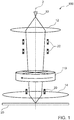
- Fig. 1 shows a scanning charged particle beam device 100.
- the charged particle beam device includes an emitter 10 for emitting a charged particle beam, for example an electron beam, along an optical axis 2.
- the emitter has an emitter tip, which is focused on a specimen 20 with a lens assembly.
- the lens assembly consists of a condenser lens 12 and an objective lens 14.
- the condenser lens can also be replaced by a condenser lens assembly having one, two or three condenser lenses. Thereby, a lens assembly with rotational symmetric lenses is utilized to focus that charged particle beam on the specimen 20.
- alignment deflectors 22 are provided in the charged particle beam device.
- alignment deflectors 22 which are exemplarily shown as double stage alignment deflection system in figure 1 , are shown in one direction, alignment deflectors can also be provided in a second direction, e.g. perpendicular to the paper plane in figure 1 .
- a scanning deflector 30 is provided for scanning the charged particle beam over the specimen 20.
- alignment deflectors and/or scanning deflectors can be magnetic (as shown in FIG.1 ), electrostatic or combined electrostatic-magnetic.
- the charged particle beam device 100 further includes a compensation assembly for compensating mechanical, magnetic and/or electrostatic inaccuracies in the device.
- the compensation assembly 110 is shown as a rotatable octopole element.
- the compensation assembly is adapted for compensating a four-fold astigmatism and has at least an eight-pole compensation capability.
- a first octopole element and a second octopole element acting in respective different directions, a rotatable octopole element, and an element having at least 12 poles, for example 16 poles, can be provided.
- inaccuracies for example mechanical, magnetic and/or electrostatic inaccuracies
- corrections of aberrations the coefficients Cs and Cc, which describe deviations of linear optics, i.e. spherical aberration and chromatic aberration are compensated. It has been shown by Otto Scherzer in 1940 that the two coefficients Cs and Cc are always positive and not equal to zero for rotational symmetric, time independent, and space charge free lenses. Embodiments described herein relate to systems, such as EBI columns, which fulfill all three conditions. This is one existing difference as compared to systems including aberration correction.
- the compensation assembly acts on an essentially round beam and is positioned and adapted to act on an essentially round beam. This is different as compared to systems having higher order elements for compensating spherical and/or chromatic aberrations.
- the common principle of the compensations described herein and the correction of spherical and chromatic aberrations is the utilization of higher order multipoles.
- predetermined corrective contributions to the coefficients Cs and Cc are generated to compensate these coefficients.
- deviations in the focusing properties which do not exist in the above described theory in light of the rotational symmetry, and which continue to exist after correction of the coefficients Cs and Cc has been carried out.
- Such inaccuracies can be mechanical manufacturing imperfections, misalignment of optical components, material inhomogenities, imperfections of the electric and magnetic fields used for focusing, aligning and adjusting, contaminations and charging of beam steering components, etc.
- rotational lenses and fields are typically referred to as essentially rotational symmetric within the present disclosure.
- the resulting field distortions can be described by a multipole expansion, and the multipole components can be beneficially corrected as described herein.
- a deflection of the beam can be corrected with a dipole, for example the deflector 22 as shown in figure 1 , and as known in the art.
- An axial astigmatism can be corrected with a quadrupole, for example a stigmators, and as also known in the art.
- a three-fold astigmatism can be corrected with a hexapole, for example with a hexapole-stigmator.
- a four-fold astigmatism can be corrected with an octopole, for example an octopole-stigmator.
- a further difference as compared to correction of spherical and chromatic aberration is the beneficial utilization of the embodiments described herein in electron beam inspection systems.
- Aberration correction aims at increase of the numerical aperture in order to improve resolution of the system. Thereby, the depth of focus is reduced.
- Electron beam inspection systems i.e., EBI systems, already use, according to embodiments described herein, a numerical aperture in a range of 10 to 70mrad. This is due to the fact that beam currents in a range of 10 to 500nA are provided such that electron-electron-interaction has a sufficiently large contribution to the beam diameter, i.e. the resolution. Thus, numerical apertures are already increased to the above-mentioned range for best performance.
- the depth of focus is in a range of 0.1 to 1 ⁇ m.
- a further decrease of the depth of focus would jeopardize electron beam inspection, which is typically conducted on-the-fly, wherein deviations from a flat wafer surface cannot be corrected for at that desired inspection speeds and, thus, need to be within the depth of focus.
- the methods according to typical embodiments described herein and that apparatuses according to typical embodiments described herein can be beneficially utilized for numerical apertures, beam currents, and depths of focus in the above-mentioned ranges.
- a compensating octopole field of adjustable strength and orientation is provided for embodiments described herein.
- the octopole device according to the invention is located at a position of sufficient beam diameter with an essentially round beam and co-axially with the beam axis (otherwise it will generate defocus, beam deflection, and 1st & 2nd order astigmatism).
- the beam diameter at the position of the compensation assembly is in a range of 50 to 500 ⁇ m.
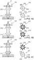
- the two orthogonal octopole fields can be either magnetic or electrostatic or both. Possible configurations are described with respect to FIGS. 1 , and 2A to 4C .
- figure 1 shows the compensation assembly 110 which is axially aligned with the beam axis 2 and which is located at a position with a sufficient diameter of the charged particle beam.
- the compensation assembly 110 as shown in figure 1 is a magnetic or electrostatic octopole, which can be rotated around its axis and/or the optical axis 2, respectively.
- the compensation assembly is provided by two octopoles 210 and 211 which are provided at a single position along the axis 2 and within two planes such that the fields of the first octopole 210 and the second octopole 211 overlap essentially.
- the position along the axis 2 of one octopole is in the area where the strength of the electrostatic field of the other octopole element, or in figures 2B and 2C the electrostatic and/or magnetic field, is 50% or more of the maximum field strengths.
- each of the electrostatic octopoles includes eight electrodes 220, which are configured to be individually biased.
- the second octopole 211 is rotated with respect to the first octopole 210 by an angle such as 22.5°.
- two magnetic octopoles 212 and 213 are provided similarly to the octopoles 210 and 211 in figure 2A .
- Each of the octopoles 212 and 213 includes eight coils 240.
- the octopoles are rotated with respect to each other by an angle such as 22.5°, as illustrated by axes 230.
- Figure 2C shows a combined electrostatic magnetic compensation assembly 110, wherein an electrostatic octopole 210 is combined with a magnetic octopole 213. Both octopoles are provided at the single position within two planes along the axis 2.
- the octopole 210 includes eight electrodes 220.
- the octopole 213 includes eight coils 240. In light of the fact that the electrostatic field and the magnetic field are orthogonal to each other in an electro-magnetic sense, the two octopoles are not rotated with respect to each other.
- the magnetic octopole 213 can also be provided in the plane above the electrostatic octopole 210, i.e. the two octopoles in figure 2C switch their position.
- Figures 3A to 3C show further embodiments of scanning charged particle beam devices 100.
- the charged particle beam device can include a condenser lens assembly 12 having more than one condenser lens.
- the examples shown in figures 3A to 3C have a first condenser lens 312A and a second condenser lens 312B. Accordingly, typical modifications of embodiments described herein may have more than one condenser lens.
- the lens assembly consists of condenser lens or a condenser lens assembly and of an objective lens. As shown in FIGS.
- a cross-over of the charged particle beam can be generated in the condenser lens assembly 12, typically between a first condenser lens 312A and a further condenser lens, e.g. the second condenser lens 312B. All lenses in the lens assembly for focusing the charged particle beam on the specimen are rotational symmetric. Accordingly, no astigmatic images are generated in the beam path from the emitter to the specimen. According to some typical modifications of embodiments described herein, the lens assembly is configured for, and operated such that no cross over is generated from the emitter to the specimen. For example the lens system results in an essentially telecentric beam path.
- the charged particle beam devices and methods of operating thereof do not include astigmatic lenses.
- an astigmatism might result in line foci, which are directly adjacent to each other, i.e. within 1 mm or less, typically within a few 100 ⁇ m or less.
- the charged particle beam devices and methods of operating thereof do not include astigmatic lenses configured, adapted, positioned in a column and/or operated such that line foci having a macroscopic distance of, for example, 10 mm or above, such as 30 to 80 mm are generated, i.e. intentionally generated.
- the compensation assemblies 110 shown in figures 3A to 3C are provided at a single position and in one plane.
- Figure 3A illustrates embodiments where the compensation assembly 110 includes 12 electrodes 320.
- the compensation assembly 110 can include 12 coils 340.
- Figure 3B illustrates embodiments where the compensation assembly 110 includes 16 electrodes 320.
- the compensation assembly 110 can include 16, 340.
- Figure 3C illustrates embodiments where the compensation assembly 110 includes eight electrodes 320 in combination with eight coils 340.
- the coils can be wound on pole pieces, which act as electrodes.
- the electrodes and coils can be provided at the same rotational position in order to provide 16 poles capable of generating an octopole field that can be controlled in strength and orientation.
- the 12 poles or 16 poles, respectively, as shown in figures 3A to 3C can generally be controlled such that an octopole field can be generated, which is variable in field strength and orientation, i.e. rotational orientation around axis 2 of the scanning charged particle beam device 100.
- a compensating octopole field of adjustable strength and orientation is provided at a position, which is co-axially with the lens assembly and at a position with a sufficiently large beam diameter of an essentially round beam in order to correct for deviations from a perfect rotational symmetry.
- two orthogonal octopole fields can be either magnetic or electrostatic or both and can be provided at two positions and in two separate planes.
- the compensation assembly is provided by two octopoles 210 and 211 which are provided at two positions along the axis 2 and within two planes such that the fields of the first octopole 210 and the second octopole 211 do not overlap essentially, for example, such that the position along the axis 2 of one octopole is in the area where the strength of the electrostatic field of the other octopole element, or in figures 4B and 4C the electrostatic and/or magnetic field, is 20% or less of the maximum field strengths.
- each of the electrostatic octopoles includes eight electrodes 220, which are configured to be individually biased.
- the second octopole 211 is rotated with respect to the first octopole 210 by an angle, which is provided by 22.5° plus the angle of a lamor rotation of the beam in the system.
- two magnetic octopoles 212 and 213 are provided similarly to the octopoles 210 and 211 in figure 4A .
- Each of the octopoles 212 and 213 includes eight coils 240.
- the octopoles are rotated with respect to each other by an angle, which is provided by 22.5° plus the angle of a lamor rotation of the beam in the system.
- Figure 4C shows a combined electrostatic magnetic compensation assembly 110, wherein an electrostatic octopole 211 is combined with that magnetic octopole 212. Both octopoles are provided at the two positions within two planes along the axis 2.
- the octopole 211 includes eight electrodes 220.
- the octopole 212 includes eight coils 240.
- the magnetic octopole 212 can also be provided in the plane below the electrostatic octopole 211, i.e. the two octopoles in figure 4C switch their position.
- the fields can be generated by a single element providing both octopole directions or two separated elements - in essentially one plane or in two planes separated along the optical axis - one for each direction.
- a possibly existing Larmor rotation between the locations of the two elements must be taken into account to ensure orthogonality.
- two elements they both have at least 8 electrodes or pole pieces. If a single element is used, it includes more than 8 pole pieces. With 16 pole pieces the orthogonal fields can be generated independently, but a lower number of poles (e.g. 12) is also sufficient if the excitation of the poles is properly adjusted.
- the compensation assembly can also be used to generate one, more, or all lower order correction fields (defocus, deflection, 1st & 2nd order astigmatism). Therefore the compensation assembly as described herein can replace some of the other compensation components in a column. Particularly for electrostatic octopole elements, lower order correction fields might be additionally generated by the octopole. In this case, other elements, preferably all other elements, in the corrections assembly can be emitted. Utilizing an electrostatic octopole, all desired multi-poles can be generated concentric on a desired optical axis, such that iterative alignment procedures might not be necessary. For deviating axes of the different orders of correction, an iterative alignment procedure is beneficial because, e.g., a 2nd order astigmatism compensation might necessitate a further correction of the deflection
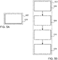
- Fig. 5A shows a flow chart illustrating embodiments for methods of compensating mechanical, magnetic and/or electrostatic inaccuracies in a scanning charged particle beam device.
- step 502 an alignment procedure is conducted, wherein the alignment procedure includes compensating 4-fold astigmatism with an element having at least 8-pole compensation capability, wherein the aligning and compensating steps of the alignment procedure act on an the charged particle beam with beam dimensions in two orthogonal directions each of at least 50 ⁇ m and coaxially aligned with at least the element having at least the 8-pole compensation capability.
- the alignment procedure can include, as shown in FIG. 5B , and wherein the steps are provided in this order: aligning a charged particle beam to be scanned over a specimen to an optical axis as indicated by step 506, compensating axial astigmatism with an element having at least 4-pole compensation capability as indicated by step 508, compensating 3-fold astigmatism with an element having at least 6-pole compensation capability as indicated by step 510, and compensating 4-fold astigmatism with an element having at least 8-pole compensation capability as indicated by step 504, wherein the aligning and compensating steps of the alignment procedure act on an the charged particle beam with beam dimensions in two orthogonal directions each of at least 50 ⁇ m and coaxially aligned with at least the element having at least the 8-pole compensation capability.
- the alignment procedure can further include fine focusing of the charged particle beam on the specimen after aligning the charged particle beam and before compensating the axial astigmatism.
- Providing the alignment step in this order allows for higher order compensation, because the higher order influences of the inaccuracies are typically not visible as long as a lower order influence of the inaccuracies are not compensated for.
- embodiments of scanning charged particle beam devices and of method of compensating inaccuracies provide a compensation assembly and/or a compensation procedure, wherein the 8-pole compensation capability is provided by an octopole field, which is adjustable in azimuth angle and field strength.
- the alignment procedure does not include a correction of spherical aberration and/or chromatic aberration and a compensation of aberration coefficients Cs and/or Cc.
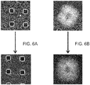
- FIGS. 6A and 6B each show a comparison of image quality using state-of-the-art beam alignment including split align, quadrupole & hexapole stigmation and coma correction.
- FIG. 6A shows in the upper figure, with a state of the art alignment an asymmetry of the spot, which is e.g. in this case is caused by aperture contamination.
- Figure 6B is a close-up of a small particle in under focus condition. Instead of being uniformly blurred, the particle appears as a squarish ring with four pronounced intensity maxima around a darker center.
- Embodiments described herein particularly when being utilized in or as an electron beam inspection system (EBI), which is considered a common term in the respective technical field, provide a high current electron beam probe with a simple optics, e.g. without Cc and Cs correction.
- EBI electron beam inspection system
- the beam is intended to be fully rotational symmetric in the column in order to provide optimized focus of a round electron probe on the specimen.
- Imperfections e.g.
- FIG. 7 illustrates a device 700 with a plurality of charged particle beam emitters 10 for emitting a plurality of charged particle beams.
- the multi-charged particle beam device can be utilized as an electron beam inspection (EBI) device. Utilizing a plurality of charged particle beams is beneficial for EBI because inspection of entire wafers is critical with respect to wafer throughput. Measurement speed for full inspection is critical to avoid a bottle neck for semiconductor manufacturing and the like. Accordingly, it is beneficial to provide a multi-beam device with high beam currents, wherein the beam spot symmetry is compensated with a compensation assembly according to embodiments described herein.
- Figure 7 shows the multi-charged particle beam device 700 having a vacuum chamber 706 to provide a beam column for the plurality of beams.
- a multi-charged particle beam device 700 can include an objective lens 714, having one excitation coil 715 for exciting a pole piece assembly.
- the pole piece assembly typically includes an upper pole piece and a lower pole piece.
- the pole piece includes an opening for each beam, i.e. there is one opening per beam.
- Each beam travels though the respective opening past the upper pole piece and past the lower pole piece in this opening.
- the objective lens is typically a decelerating combined electrostatic magnetic lens.
- FIG. 7 for each beam an upper electrode 718 and a lower electrode 717 forming an immersion lens are shown.
- the common objective lens focuses the plurality of beams on the specimen 20, which is provided on a specimen stage.
- characteristics, arrangements and other properties described with respect to the single beam columns above can similarly be applied to the multi beam device. Accordingly, compensation assemblies 110 as described herein are provided for each of the electron beams.
- a transition from single-beam devices to multi-beam devices might have one exception. Since the device 700 shown in FIG. 7 has a common objective lens, the objective lens might not have a full rotational symmetry with respect to each beam. However, the basic optical parameters of each sub-lens (focal length, aberration coefficients Cs and Cc) are essentially the same as for an ideally rotational symmetric lens with the same mechanical dimensions of the field-forming pole pieces, and the above described omission of astigmatic images etc. still occurs. It is to be understood, that for the objective lens 714 shown in FIG. 714 the rotational symmetry of the focusing properties is maintained to as far as possible and as described in more detail below.
- the properties of the lens is less influenced by an asymmetry of the outer areas of the lens or a pole piece and the rotational properties are still provided for the openings to which the magnetic field is guided for acting on the beams passing through the opening.
- the deviation from a fully rotational symmetric round lens e.g. for a single beam, occurs only for higher order deviations, for example 3rd order deviations, and e.g. as a fourfold astigmatism, which can be compensated for with the compensation assembly according to embodiments described herein.
- an optical system for a charged particle column includes an objective lens with an electrostatic lens component and a magnetic lens component. Each component comprises at least two sub-lenses, whereby by each sub-lens a charged particle beams is focused.
- an optical system for a plurality of charged particle beams is provided.
- the charged particle optical system comprises at least two separate magnetic lens field areas and at least two separate electrostatic lens field areas in an objective lens 714. Thereby, the at least two separate magnetic lens field areas are driven by a common excitation coil 715. At least two charged particle beams travel through the optical system, each through a separate opening in the optical system.
- the at least two charged particle beams traveling through the at least two openings are focused or imaged each within one of the at least two magnetic lens field areas and within one of the at least two electrostatic lens field areas.
- an opening in the optical system is to be understood as respective openings or holes in the components of the optical system. These holes in the components are located such with respect to each other, that a charged particle beam can travel through these holes. Thereby, the hole in the components are not meant to be strictly within on line, since the direction of a charged particle beam can corrected for e.g. by using deflection means.
- a charged particle beam device 700 can have a magnetic lens component.
- This magnetic lens component comprises an excitation coil 715.
- the diameter of this coil can be about 100 mm to 1000 mm. Thereby, the coil diameter depends in general on the number of electron beams focused by the objective lens 714.
- an electrostatic lens component provided by elements 717 and 718.
- the lens system can be described as a plurality of sub-lenses for each of the electron beams.
- each of the electrostatic immersion sub-lenses of the electrostatic lens component comprises an upper electrode 718 and a lower electrode 717. These electrodes should be made of a non-magnetic conductive material.
- the electrodes 718 and 717 are controlled to decelerate the electron beam for impingement on the specimen 20 with a desired landing energy.
- the deceleration of the primary electron beam in, e.g. an objective lens has two different effects. First, the electrons impinge on a specimen with reduced energy. Second, the electrons travel through the optical system with higher beam energy. Due to a retarding field, the electron energy of an electron impinging on a specimen can be reduced. This is especially relevant for imaging and inspection purposes.
- a specimen to be imaged e.g. an integrated circuit, is preferably not charged by the electron beam. Therefore, however, the beam energy has to be reduced to obtain a balance between emitted secondary electrons and accepted primary electrons.
- the higher beam energy above and partly within the optical system can be advantageous.
- Aberrations and influences of the so-called Boersch effect are reduced by higher beam energies.
- chromatic aberrations depend on ⁇ E/E.
- ⁇ E is the energy spread of an electron beam. This energy spread or energy variation might be introduced by an electron gun or by a variation of acceleration voltages.
- the mean electron beam energy E can be increased. Thereby, chromatic aberrations are decreased.
- a high beam energy above one to several keV before and during the focusing is advantageous.
- the common objective lens 714 can also be provided by a "sliced objective lens". Examples of such a lens structure are described in EP 1 432 007 B1 , which issued March 10, 2010.
- a lens system i.e. an objective lens for a charged particle column is provided.
- the lens system includes at least two lens modules.
- the at least two lens modules share a single common excitation coil.
- Each lens module comprises a first and second pole piece and an opening for a charged particle beam.
- the lens modules can be separately manufactured and are provided next to each other to form the objective lens.
- Providing separate pole piece modules provides easier manufacturing of a common objective lens for a plurality of beams.
- an objective lens for a plurality of charged particle beams comprises at least two individual lens modules, as e.g. described in EP 1 432 007 B1 .
- Each lens module includes a first pole piece, a second pole piece and at least one opening for a charged particle beam.
- the objective lens includes at least one single common excitation coil providing a magnetic flux to the at least two lens modules.
- the condenser lens assembly and the objective lens which are described as rotationally symmetric with respect to FIG. 1 might have a four-fold symmetry in the event a multi-beam lens with individual modules is provided.
- this does still provide for a maximum rotational symmetry in the given system and is contrary to astigmatic images, which are an intended loss of rotational symmetry for aberration correction systems..
- Methods for compensating and charged particle beam devices with compensation assemblies provide compensations other than correction of spherical and chromatic aberrations.
- predetermined corrective contributions to the coefficients Cs and Cc are generated to compensate these coefficients.
- deviations from rotational properties are compensated for.
- Such inaccuracies can be mechanical manufacturing imperfections, misalignment of optical components, material inhomogenities, imperfections of the electric and magnetic fields used for focusing, aligning and adjusting, contaminations and charging of beam steering components, etc. These inaccuracies result in loss of perfect rotational symmetry. Compensation assemblies described herein are adapted to correct for such higher order inaccuracies.
Landscapes
- Physics & Mathematics (AREA)
- Chemical & Material Sciences (AREA)
- Analytical Chemistry (AREA)
- Spectroscopy & Molecular Physics (AREA)
- Engineering & Computer Science (AREA)
- General Engineering & Computer Science (AREA)
- High Energy & Nuclear Physics (AREA)
- Electron Beam Exposure (AREA)
- Electron Sources, Ion Sources (AREA)
Claims (13)
- Vorrichtung zum Ausgleichen mechanischer, magnetischer oder elektrostatischer Ungenauigkeiten in einer Abtastvorrichtung für einen Strahl geladener Teilchen, Folgendes umfassend:eine Ausrichtungsprozedur (502), die umfasst:einen 4-fachen Astigmatismus mit einem Element auszugleichen (504), das zumindest eine 8-polige Ausgleichsfähigkeit hat;wobei der Ausgleichsschritt der Ausrichtungsprozedur an einem Strahl geladener Teilchen mit Strahlabmessungen in zwei orthogonalen Richtungen jeweils von mindestens 50 µm und koaxial ausgerichtet mit zumindest dem Element erfolgt, das zumindest die 8-polige Ausgleichsfähigkeit hat.
- Verfahren nach Anspruch 1, wobei die Ausrichtungsprozedur darüber hinaus die folgenden Schritte umfasst, die in dieser Reihenfolge und vor dem Ausgleichen des 4-fachen Astigmatismus durchgeführt werden:einen Strahl geladener Teilchen, der abtastend über eine Probe gelenkt werden soll, auf eine optische Achse auszurichten (506); einen axialen Astigmatismus mit einem Element auszugleichen (508), das zumindest eine 4-polige Ausgleichsfähigkeit hat; und einen 3-fachen Astigmatismus mit einem Element auszugleichen (510), das zumindest eine 6-polige Ausgleichsfähigkeit hat.
- Verfahren nach Anspruch 2, wobei die Ausrichtungsprozedur darüber hinaus eine Feinfokussierung des Strahls geladener Teilchen auf die Probe umfasst, nachdem der Strahl geladener Teilchen ausgerichtet wurde und bevor der axiale Astigmatismus ausgeglichen wird.
- Verfahren nach einem der Ansprüche 1 bis 3, wobei die Ausrichtungsprozedur oder ein Teil der Ausrichtungsprozedur zweimal oder mehrmals iterativ durchgeführt wird, derart, dass zwei oder mehr der Schritte in der Ausrichtungsprozedur iterativ durchgeführt werden.
- Verfahren nach einem der Ansprüche 1 bis 4, wobei die 8-polige Ausgleichsfähigkeit hat durch ein Oktopolfeld bereitgestellt wird, das im Azimutwinkel und in der Stärke einstellbar ist.
- Verfahren nach einem der Ansprüche 1 bis 5, wobei das Verfahren darüber hinaus umfasst: die numerische Apertur des Systems auf einen Wert von 10 bis 70 mrad einzustellen.
- Verfahren nach einem der Ansprüche 1 bis 6, wobei die Abtastvorrichtung für einen Strahl geladener Teilchen einen Strahlengang ohne ein astigmatisches Zwischenbild hat.
- Verfahren nach einem der Ansprüche 1 bis 7, wobei die Abtastvorrichtung für einen Strahl geladener Teilchen einen Strahlengang ohne Überkreuzung zwischen einer Objektivlinse und einer Kondensorlinse einer Kondensorlinsenanordnung hat, wobei es sich bei der Kondensorlinse um die Kondensorlinse der Kondensorlinsenanordnung handelt, die der Objektivlinse am nächsten ist.
- Abtastvorrichtung (100) für einen Strahl geladener Teilchen, Folgendes aufweisend:einen Emitter (10) mit mindestens einer Emitterspitze, die dazu ausgelegt ist, einen Strahl geladener Teilchen abzugeben;eine Linsenanordnung, die dazu ausgelegt ist, die Emitterspitze auf eine Probe (20) zu fokussieren, wobei die Fokussieranordnung aus einer Kondensorlinsenanordnung (12) und einer Objektivlinse (14) besteht, wobei die Kondensorlinsenanordnung (12) und die Objektivlinse (14) rotationssymmetrisch sind;eine Ausgleichsanordnung (110), um mechanische, magnetische oder elektrostatische Ungenauigkeiten auszugleichen, wobei die Ausgleichsanordnung mindestens ein Element aufweist, das aus der Gruppe ausgewählt ist, die besteht aus: einem ersten Oktopolelement und einem zweiten Oktopolelement, die in jeweils unterschiedlichen Richtungen wirken, einem drehbaren Oktopolelement; und einem Element, bei dem es sich um zumindest ein 12-poliges Element handelt, wobei im Gebrauch der Vorrichtung (100) die Ausgleichsanordnung (110) dazu ausgelegt ist, auf den Strahl geladener Teilchen mit Strahlabmessungen in zwei orthogonalen Richtungen jeweils von mindestens 50 µm und koaxial ausgerichtet mit zumindest dem einen Element einzuwirken.
- Vorrichtung (100) nach Anspruch 9, darüber hinaus Folgendes aufweisend: einen Abtastdeflektor (30), um den Strahl geladener Teilchen abtastend über die Probe (20) zu lenken.
- Vorrichtung (100) nach Anspruch 9 oder 10, wobei die Ausrichtungsanordnung darüber hinaus aufweist:eine zweidimensionale Ausrichtungsdeflektoreinheit;einen zweidimensionalen Stigmator; undein zweidimensionales Hexapolelement, um einen 3-fachen Astigmatismus auszugleichen.
- Vorrichtung nach einem der Ansprüche 9 bis 11, wobei die numerische Apertur des Systems 10 bis 70 mrad beträgt.
- Vorrichtung nach einem der Ansprüche 9 bis 12, wobei die Abtastvorrichtung (100) für einen Strahl geladener Teilchen keine Linsen zum Erzeugen astigmatischer Bilder enthält.
Priority Applications (4)
| Application Number | Priority Date | Filing Date | Title |
|---|---|---|---|
| EP12188686.5A EP2722868B1 (de) | 2012-10-16 | 2012-10-16 | Oktopolvorrichtung und -verfahren zur spotgrössenverbesserung |
| US13/663,692 US8816270B2 (en) | 2012-10-16 | 2012-10-30 | Octopole device and method for spot size improvement |
| TW102134138A TWI503858B (zh) | 2012-10-16 | 2013-09-23 | 用於改善光點大小的八極裝置及方法 |
| JP2013214365A JP5738378B2 (ja) | 2012-10-16 | 2013-10-15 | オクタポール装置及びスポットサイズ向上方法 |
Applications Claiming Priority (1)
| Application Number | Priority Date | Filing Date | Title |
|---|---|---|---|
| EP12188686.5A EP2722868B1 (de) | 2012-10-16 | 2012-10-16 | Oktopolvorrichtung und -verfahren zur spotgrössenverbesserung |
Publications (2)
| Publication Number | Publication Date |
|---|---|
| EP2722868A1 EP2722868A1 (de) | 2014-04-23 |
| EP2722868B1 true EP2722868B1 (de) | 2018-02-21 |
Family
ID=47358341
Family Applications (1)
| Application Number | Title | Priority Date | Filing Date |
|---|---|---|---|
| EP12188686.5A Active EP2722868B1 (de) | 2012-10-16 | 2012-10-16 | Oktopolvorrichtung und -verfahren zur spotgrössenverbesserung |
Country Status (4)
| Country | Link |
|---|---|
| US (1) | US8816270B2 (de) |
| EP (1) | EP2722868B1 (de) |
| JP (1) | JP5738378B2 (de) |
| TW (1) | TWI503858B (de) |
Families Citing this family (12)
| Publication number | Priority date | Publication date | Assignee | Title |
|---|---|---|---|---|
| US20130058446A1 (en) * | 2011-06-10 | 2013-03-07 | Xian-Jun Zheng | Continuous fusion due to energy concentration through focusing of converging fuel particle beams |
| JP2014232082A (ja) * | 2013-05-30 | 2014-12-11 | 株式会社東芝 | パターン検査方法及びパターン検査装置 |
| WO2016145458A1 (en) * | 2015-03-10 | 2016-09-15 | Hermes Microvision Inc. | Apparatus of plural charged-particle beams |
| US9691588B2 (en) | 2015-03-10 | 2017-06-27 | Hermes Microvision, Inc. | Apparatus of plural charged-particle beams |
| JP6703092B2 (ja) * | 2015-07-22 | 2020-06-03 | エーエスエムエル ネザーランズ ビー.ブイ. | 複数荷電粒子ビームの装置 |
| US10276346B1 (en) * | 2016-03-09 | 2019-04-30 | Kla-Tencor Corporation | Particle beam inspector with independently-controllable beams |
| US11062874B2 (en) * | 2016-12-30 | 2021-07-13 | Asml Netherlands B.V. | Apparatus using multiple charged particle beams |
| US10283315B2 (en) * | 2017-05-16 | 2019-05-07 | International Business Machines Corporation | Measuring spherical and chromatic aberrations in cathode lens electrode microscopes |
| KR20240097977A (ko) * | 2017-09-29 | 2024-06-27 | 에이에스엠엘 네델란즈 비.브이. | 하전 입자 빔 검사를 위한 샘플 사전-충전 방법들 및 장치들 |
| JP7057220B2 (ja) * | 2018-05-24 | 2022-04-19 | 株式会社ニューフレアテクノロジー | マルチ電子ビーム画像取得装置及びマルチ電子ビーム光学系の位置決め方法 |
| US10748739B2 (en) * | 2018-10-12 | 2020-08-18 | Kla-Tencor Corporation | Deflection array apparatus for multi-electron beam system |
| CN109585244B (zh) * | 2018-10-23 | 2021-09-14 | 中国科学院电工研究所 | 高功率密度的电子束聚焦装置 |
Citations (6)
| Publication number | Priority date | Publication date | Assignee | Title |
|---|---|---|---|---|
| EP0500179A1 (de) | 1991-02-20 | 1992-08-26 | Koninklijke Philips Electronics N.V. | Ladungspartikelbündelanordnung |
| EP1335402A2 (de) | 2002-02-08 | 2003-08-13 | Jeol Ltd. | Wienfilter und damit ausgerüstetem Elektronenmikroskop |
| EP1432006A2 (de) | 2002-12-17 | 2004-06-23 | Jeol Ltd. | Energiefilter und Elektronenmikroskop |
| US6784437B2 (en) | 2001-12-04 | 2004-08-31 | Leo Elektronenmikroskopie Gmbh | Corrector for correcting first-order chromatic aberrations of the first degree |
| US7807965B2 (en) | 2007-12-05 | 2010-10-05 | Ceos Corrected Electron Optical Systems Gmbh | Corrector for axial and off-axial beam paths |
| US20110192976A1 (en) * | 2010-02-10 | 2011-08-11 | Halcyon Molecular, Inc. | Aberration-correcting dark-field electron microscopy |
Family Cites Families (5)
| Publication number | Priority date | Publication date | Assignee | Title |
|---|---|---|---|---|
| JP3254906B2 (ja) * | 1994-06-27 | 2002-02-12 | 富士通株式会社 | 荷電粒子ビーム露光装置及び露光方法 |
| DE19739290A1 (de) * | 1997-09-08 | 1999-03-11 | Ceos Gmbh | Verfahren zur Beseitigung axialer Bildfehler erster, zweiter und dritter Ordnung bei Korrektur des Öffnungsfehlers dritter Ordnung in elektronen-optischen Systemen |
| EP1956631B1 (de) | 2002-12-17 | 2012-06-20 | ICT Integrated Circuit Testing Gesellschaft für Halbleiterprüftechnik mbH | Linsensystem für mehrere geladene Teilchenstrahlen |
| NL1024192C2 (nl) * | 2003-08-29 | 2005-03-01 | Fei Co | Werkwijze voor het focusseren in een deeltjes-optisch toestel met behulp van astigmatisme in de deeltjesbundel. |
| KR101364672B1 (ko) * | 2006-09-12 | 2014-02-19 | 가부시키가이샤 에바라 세이사꾸쇼 | 하전입자선장치, 그 장치를 이용한 비점수차 조정방법 및그 장치를 이용한 디바이스제조방법 |
-
2012
- 2012-10-16 EP EP12188686.5A patent/EP2722868B1/de active Active
- 2012-10-30 US US13/663,692 patent/US8816270B2/en active Active
-
2013
- 2013-09-23 TW TW102134138A patent/TWI503858B/zh active
- 2013-10-15 JP JP2013214365A patent/JP5738378B2/ja active Active
Patent Citations (6)
| Publication number | Priority date | Publication date | Assignee | Title |
|---|---|---|---|---|
| EP0500179A1 (de) | 1991-02-20 | 1992-08-26 | Koninklijke Philips Electronics N.V. | Ladungspartikelbündelanordnung |
| US6784437B2 (en) | 2001-12-04 | 2004-08-31 | Leo Elektronenmikroskopie Gmbh | Corrector for correcting first-order chromatic aberrations of the first degree |
| EP1335402A2 (de) | 2002-02-08 | 2003-08-13 | Jeol Ltd. | Wienfilter und damit ausgerüstetem Elektronenmikroskop |
| EP1432006A2 (de) | 2002-12-17 | 2004-06-23 | Jeol Ltd. | Energiefilter und Elektronenmikroskop |
| US7807965B2 (en) | 2007-12-05 | 2010-10-05 | Ceos Corrected Electron Optical Systems Gmbh | Corrector for axial and off-axial beam paths |
| US20110192976A1 (en) * | 2010-02-10 | 2011-08-11 | Halcyon Molecular, Inc. | Aberration-correcting dark-field electron microscopy |
Non-Patent Citations (1)
| Title |
|---|
| SCHERZER: "Sphärische und chromatische Korrektur von Elektronen-Linsen", JENA, 1947, pages 114 - 132, ISSN: 0863-0259 |
Also Published As
| Publication number | Publication date |
|---|---|
| US8816270B2 (en) | 2014-08-26 |
| US20140103201A1 (en) | 2014-04-17 |
| JP2014082211A (ja) | 2014-05-08 |
| JP5738378B2 (ja) | 2015-06-24 |
| TW201417134A (zh) | 2014-05-01 |
| TWI503858B (zh) | 2015-10-11 |
| EP2722868A1 (de) | 2014-04-23 |
Similar Documents
| Publication | Publication Date | Title |
|---|---|---|
| EP2722868B1 (de) | Oktopolvorrichtung und -verfahren zur spotgrössenverbesserung | |
| KR102109963B1 (ko) | 1차 하전 입자 빔렛들의 어레이를 이용한 시료의 검사를 위한 하전 입자 빔 디바이스 및 1차 하전 입자 빔렛들의 어레이를 이용하여 시료를 이미징하거나 조명하는 방법 | |
| TWI713883B (zh) | 帶電粒子束裝置、用於帶電粒子束裝置的孔佈置和用於操作帶電粒子束裝置的方法 | |
| JP5710061B2 (ja) | 高スループットsemツール | |
| US7465939B2 (en) | Aberration correction device and method for operating same | |
| JP6278553B2 (ja) | 2次電子光学系及び検出デバイス | |
| JP2010519697A (ja) | 高スループットsemツール | |
| KR19990028770A (ko) | 입자-광학 장치에서 렌즈 수차를 교정하기 위한 교정장치 | |
| US20160189916A1 (en) | Scanning charged particle beam device having an aberration correction aperture and method of operating thereof | |
| CN115223831B (zh) | 带电粒子束设备、多子束组件和检查样本的方法 | |
| JP6737539B2 (ja) | 荷電粒子線装置 | |
| CN116325067A (zh) | 在可调工作距离附近具有快速自动对焦的多重粒子束显微镜及相关方法 |
Legal Events
| Date | Code | Title | Description |
|---|---|---|---|
| PUAI | Public reference made under article 153(3) epc to a published international application that has entered the european phase |
Free format text: ORIGINAL CODE: 0009012 |
|
| AK | Designated contracting states |
Kind code of ref document: A1 Designated state(s): AL AT BE BG CH CY CZ DE DK EE ES FI FR GB GR HR HU IE IS IT LI LT LU LV MC MK MT NL NO PL PT RO RS SE SI SK SM TR |
|
| AX | Request for extension of the european patent |
Extension state: BA ME |
|
| 17P | Request for examination filed |
Effective date: 20140605 |
|
| RBV | Designated contracting states (corrected) |
Designated state(s): AL AT BE BG CH CY CZ DE DK EE ES FI FR GB GR HR HU IE IS IT LI LT LU LV MC MK MT NL NO PL PT RO RS SE SI SK SM TR |
|
| STAA | Information on the status of an ep patent application or granted ep patent |
Free format text: STATUS: EXAMINATION IS IN PROGRESS |
|
| 17Q | First examination report despatched |
Effective date: 20170131 |
|
| GRAP | Despatch of communication of intention to grant a patent |
Free format text: ORIGINAL CODE: EPIDOSNIGR1 |
|
| STAA | Information on the status of an ep patent application or granted ep patent |
Free format text: STATUS: GRANT OF PATENT IS INTENDED |
|
| RIC1 | Information provided on ipc code assigned before grant |
Ipc: H01J 37/153 20060101AFI20170728BHEP Ipc: G21K 1/093 20060101ALI20170728BHEP |
|
| INTG | Intention to grant announced |
Effective date: 20170829 |
|
| GRAS | Grant fee paid |
Free format text: ORIGINAL CODE: EPIDOSNIGR3 |
|
| GRAA | (expected) grant |
Free format text: ORIGINAL CODE: 0009210 |
|
| STAA | Information on the status of an ep patent application or granted ep patent |
Free format text: STATUS: THE PATENT HAS BEEN GRANTED |
|
| AK | Designated contracting states |
Kind code of ref document: B1 Designated state(s): AL AT BE BG CH CY CZ DE DK EE ES FI FR GB GR HR HU IE IS IT LI LT LU LV MC MK MT NL NO PL PT RO RS SE SI SK SM TR |
|
| REG | Reference to a national code |
Ref country code: GB Ref legal event code: FG4D |
|
| REG | Reference to a national code |
Ref country code: CH Ref legal event code: EP |
|
| REG | Reference to a national code |
Ref country code: AT Ref legal event code: REF Ref document number: 972566 Country of ref document: AT Kind code of ref document: T Effective date: 20180315 |
|
| REG | Reference to a national code |
Ref country code: IE Ref legal event code: FG4D |
|
| REG | Reference to a national code |
Ref country code: DE Ref legal event code: R096 Ref document number: 602012042976 Country of ref document: DE |
|
| REG | Reference to a national code |
Ref country code: NL Ref legal event code: FP |
|
| REG | Reference to a national code |
Ref country code: LT Ref legal event code: MG4D |
|
| REG | Reference to a national code |
Ref country code: AT Ref legal event code: MK05 Ref document number: 972566 Country of ref document: AT Kind code of ref document: T Effective date: 20180221 |
|
| PG25 | Lapsed in a contracting state [announced via postgrant information from national office to epo] |
Ref country code: ES Free format text: LAPSE BECAUSE OF FAILURE TO SUBMIT A TRANSLATION OF THE DESCRIPTION OR TO PAY THE FEE WITHIN THE PRESCRIBED TIME-LIMIT Effective date: 20180221 Ref country code: CY Free format text: LAPSE BECAUSE OF FAILURE TO SUBMIT A TRANSLATION OF THE DESCRIPTION OR TO PAY THE FEE WITHIN THE PRESCRIBED TIME-LIMIT Effective date: 20180221 Ref country code: NO Free format text: LAPSE BECAUSE OF FAILURE TO SUBMIT A TRANSLATION OF THE DESCRIPTION OR TO PAY THE FEE WITHIN THE PRESCRIBED TIME-LIMIT Effective date: 20180521 Ref country code: FI Free format text: LAPSE BECAUSE OF FAILURE TO SUBMIT A TRANSLATION OF THE DESCRIPTION OR TO PAY THE FEE WITHIN THE PRESCRIBED TIME-LIMIT Effective date: 20180221 Ref country code: HR Free format text: LAPSE BECAUSE OF FAILURE TO SUBMIT A TRANSLATION OF THE DESCRIPTION OR TO PAY THE FEE WITHIN THE PRESCRIBED TIME-LIMIT Effective date: 20180221 Ref country code: LT Free format text: LAPSE BECAUSE OF FAILURE TO SUBMIT A TRANSLATION OF THE DESCRIPTION OR TO PAY THE FEE WITHIN THE PRESCRIBED TIME-LIMIT Effective date: 20180221 |
|
| PG25 | Lapsed in a contracting state [announced via postgrant information from national office to epo] |
Ref country code: AT Free format text: LAPSE BECAUSE OF FAILURE TO SUBMIT A TRANSLATION OF THE DESCRIPTION OR TO PAY THE FEE WITHIN THE PRESCRIBED TIME-LIMIT Effective date: 20180221 Ref country code: RS Free format text: LAPSE BECAUSE OF FAILURE TO SUBMIT A TRANSLATION OF THE DESCRIPTION OR TO PAY THE FEE WITHIN THE PRESCRIBED TIME-LIMIT Effective date: 20180221 Ref country code: BG Free format text: LAPSE BECAUSE OF FAILURE TO SUBMIT A TRANSLATION OF THE DESCRIPTION OR TO PAY THE FEE WITHIN THE PRESCRIBED TIME-LIMIT Effective date: 20180521 Ref country code: SE Free format text: LAPSE BECAUSE OF FAILURE TO SUBMIT A TRANSLATION OF THE DESCRIPTION OR TO PAY THE FEE WITHIN THE PRESCRIBED TIME-LIMIT Effective date: 20180221 Ref country code: LV Free format text: LAPSE BECAUSE OF FAILURE TO SUBMIT A TRANSLATION OF THE DESCRIPTION OR TO PAY THE FEE WITHIN THE PRESCRIBED TIME-LIMIT Effective date: 20180221 Ref country code: GR Free format text: LAPSE BECAUSE OF FAILURE TO SUBMIT A TRANSLATION OF THE DESCRIPTION OR TO PAY THE FEE WITHIN THE PRESCRIBED TIME-LIMIT Effective date: 20180522 |
|
| PG25 | Lapsed in a contracting state [announced via postgrant information from national office to epo] |
Ref country code: RO Free format text: LAPSE BECAUSE OF FAILURE TO SUBMIT A TRANSLATION OF THE DESCRIPTION OR TO PAY THE FEE WITHIN THE PRESCRIBED TIME-LIMIT Effective date: 20180221 Ref country code: IT Free format text: LAPSE BECAUSE OF FAILURE TO SUBMIT A TRANSLATION OF THE DESCRIPTION OR TO PAY THE FEE WITHIN THE PRESCRIBED TIME-LIMIT Effective date: 20180221 Ref country code: PL Free format text: LAPSE BECAUSE OF FAILURE TO SUBMIT A TRANSLATION OF THE DESCRIPTION OR TO PAY THE FEE WITHIN THE PRESCRIBED TIME-LIMIT Effective date: 20180221 Ref country code: EE Free format text: LAPSE BECAUSE OF FAILURE TO SUBMIT A TRANSLATION OF THE DESCRIPTION OR TO PAY THE FEE WITHIN THE PRESCRIBED TIME-LIMIT Effective date: 20180221 Ref country code: AL Free format text: LAPSE BECAUSE OF FAILURE TO SUBMIT A TRANSLATION OF THE DESCRIPTION OR TO PAY THE FEE WITHIN THE PRESCRIBED TIME-LIMIT Effective date: 20180221 |
|
| REG | Reference to a national code |
Ref country code: DE Ref legal event code: R026 Ref document number: 602012042976 Country of ref document: DE |
|
| PLBI | Opposition filed |
Free format text: ORIGINAL CODE: 0009260 |
|
| PLAN | Information deleted related to communication of a notice of opposition and request to file observations + time limit |
Free format text: ORIGINAL CODE: EPIDOSDOBS2 |
|
| PLAX | Notice of opposition and request to file observation + time limit sent |
Free format text: ORIGINAL CODE: EPIDOSNOBS2 |
|
| PG25 | Lapsed in a contracting state [announced via postgrant information from national office to epo] |
Ref country code: DK Free format text: LAPSE BECAUSE OF FAILURE TO SUBMIT A TRANSLATION OF THE DESCRIPTION OR TO PAY THE FEE WITHIN THE PRESCRIBED TIME-LIMIT Effective date: 20180221 Ref country code: SM Free format text: LAPSE BECAUSE OF FAILURE TO SUBMIT A TRANSLATION OF THE DESCRIPTION OR TO PAY THE FEE WITHIN THE PRESCRIBED TIME-LIMIT Effective date: 20180221 Ref country code: SK Free format text: LAPSE BECAUSE OF FAILURE TO SUBMIT A TRANSLATION OF THE DESCRIPTION OR TO PAY THE FEE WITHIN THE PRESCRIBED TIME-LIMIT Effective date: 20180221 Ref country code: CZ Free format text: LAPSE BECAUSE OF FAILURE TO SUBMIT A TRANSLATION OF THE DESCRIPTION OR TO PAY THE FEE WITHIN THE PRESCRIBED TIME-LIMIT Effective date: 20180221 |
|
| PLAX | Notice of opposition and request to file observation + time limit sent |
Free format text: ORIGINAL CODE: EPIDOSNOBS2 |
|
| 26 | Opposition filed |
Opponent name: CARL ZEISS MICROSCOPY GMBH Effective date: 20181121 |
|
| PG25 | Lapsed in a contracting state [announced via postgrant information from national office to epo] |
Ref country code: SI Free format text: LAPSE BECAUSE OF FAILURE TO SUBMIT A TRANSLATION OF THE DESCRIPTION OR TO PAY THE FEE WITHIN THE PRESCRIBED TIME-LIMIT Effective date: 20180221 |
|
| PLBB | Reply of patent proprietor to notice(s) of opposition received |
Free format text: ORIGINAL CODE: EPIDOSNOBS3 |
|
| REG | Reference to a national code |
Ref country code: CH Ref legal event code: PL |
|
| GBPC | Gb: european patent ceased through non-payment of renewal fee |
Effective date: 20181016 |
|
| REG | Reference to a national code |
Ref country code: BE Ref legal event code: MM Effective date: 20181031 |
|
| PG25 | Lapsed in a contracting state [announced via postgrant information from national office to epo] |
Ref country code: MC Free format text: LAPSE BECAUSE OF FAILURE TO SUBMIT A TRANSLATION OF THE DESCRIPTION OR TO PAY THE FEE WITHIN THE PRESCRIBED TIME-LIMIT Effective date: 20180221 Ref country code: LU Free format text: LAPSE BECAUSE OF NON-PAYMENT OF DUE FEES Effective date: 20181016 |
|
| REG | Reference to a national code |
Ref country code: IE Ref legal event code: MM4A |
|
| PG25 | Lapsed in a contracting state [announced via postgrant information from national office to epo] |
Ref country code: BE Free format text: LAPSE BECAUSE OF NON-PAYMENT OF DUE FEES Effective date: 20181031 Ref country code: FR Free format text: LAPSE BECAUSE OF NON-PAYMENT OF DUE FEES Effective date: 20181031 Ref country code: LI Free format text: LAPSE BECAUSE OF NON-PAYMENT OF DUE FEES Effective date: 20181031 Ref country code: CH Free format text: LAPSE BECAUSE OF NON-PAYMENT OF DUE FEES Effective date: 20181031 |
|
| PG25 | Lapsed in a contracting state [announced via postgrant information from national office to epo] |
Ref country code: IE Free format text: LAPSE BECAUSE OF NON-PAYMENT OF DUE FEES Effective date: 20181016 Ref country code: GB Free format text: LAPSE BECAUSE OF NON-PAYMENT OF DUE FEES Effective date: 20181016 |
|
| PG25 | Lapsed in a contracting state [announced via postgrant information from national office to epo] |
Ref country code: MT Free format text: LAPSE BECAUSE OF NON-PAYMENT OF DUE FEES Effective date: 20181016 |
|
| PG25 | Lapsed in a contracting state [announced via postgrant information from national office to epo] |
Ref country code: TR Free format text: LAPSE BECAUSE OF FAILURE TO SUBMIT A TRANSLATION OF THE DESCRIPTION OR TO PAY THE FEE WITHIN THE PRESCRIBED TIME-LIMIT Effective date: 20180221 |
|
| PG25 | Lapsed in a contracting state [announced via postgrant information from national office to epo] |
Ref country code: PT Free format text: LAPSE BECAUSE OF FAILURE TO SUBMIT A TRANSLATION OF THE DESCRIPTION OR TO PAY THE FEE WITHIN THE PRESCRIBED TIME-LIMIT Effective date: 20180221 |
|
| PG25 | Lapsed in a contracting state [announced via postgrant information from national office to epo] |
Ref country code: HU Free format text: LAPSE BECAUSE OF FAILURE TO SUBMIT A TRANSLATION OF THE DESCRIPTION OR TO PAY THE FEE WITHIN THE PRESCRIBED TIME-LIMIT; INVALID AB INITIO Effective date: 20121016 Ref country code: MK Free format text: LAPSE BECAUSE OF NON-PAYMENT OF DUE FEES Effective date: 20180221 |
|
| PG25 | Lapsed in a contracting state [announced via postgrant information from national office to epo] |
Ref country code: IS Free format text: LAPSE BECAUSE OF FAILURE TO SUBMIT A TRANSLATION OF THE DESCRIPTION OR TO PAY THE FEE WITHIN THE PRESCRIBED TIME-LIMIT Effective date: 20180621 |
|
| APBM | Appeal reference recorded |
Free format text: ORIGINAL CODE: EPIDOSNREFNO |
|
| APBP | Date of receipt of notice of appeal recorded |
Free format text: ORIGINAL CODE: EPIDOSNNOA2O |
|
| APAH | Appeal reference modified |
Free format text: ORIGINAL CODE: EPIDOSCREFNO |
|
| APBQ | Date of receipt of statement of grounds of appeal recorded |
Free format text: ORIGINAL CODE: EPIDOSNNOA3O |
|
| P01 | Opt-out of the competence of the unified patent court (upc) registered |
Effective date: 20230505 |
|
| PGFP | Annual fee paid to national office [announced via postgrant information from national office to epo] |
Ref country code: NL Payment date: 20230922 Year of fee payment: 12 |
|
| PGFP | Annual fee paid to national office [announced via postgrant information from national office to epo] |
Ref country code: DE Payment date: 20230920 Year of fee payment: 12 |