EP2721634B1 - Procédé de passivation chimique d'une surface d'un produit de matériau semi-conducteur iii-v, et produit obtenu par un tel procédé - Google Patents
Procédé de passivation chimique d'une surface d'un produit de matériau semi-conducteur iii-v, et produit obtenu par un tel procédé Download PDFInfo
- Publication number
- EP2721634B1 EP2721634B1 EP12731132.2A EP12731132A EP2721634B1 EP 2721634 B1 EP2721634 B1 EP 2721634B1 EP 12731132 A EP12731132 A EP 12731132A EP 2721634 B1 EP2721634 B1 EP 2721634B1
- Authority
- EP
- European Patent Office
- Prior art keywords
- iii
- peak
- film
- solvent
- product
- Prior art date
- Legal status (The legal status is an assumption and is not a legal conclusion. Google has not performed a legal analysis and makes no representation as to the accuracy of the status listed.)
- Active
Links
Images
Classifications
-
- H—ELECTRICITY
- H10—SEMICONDUCTOR DEVICES; ELECTRIC SOLID-STATE DEVICES NOT OTHERWISE PROVIDED FOR
- H10P—GENERIC PROCESSES OR APPARATUS FOR THE MANUFACTURE OR TREATMENT OF DEVICES COVERED BY CLASS H10
- H10P95/00—Generic processes or apparatus for manufacture or treatments not covered by the other groups of this subclass
- H10P95/40—Treatments of semiconductor bodies to modify their internal properties, e.g. to produce internal imperfections
- H10P95/408—Treatments of semiconductor bodies to modify their internal properties, e.g. to produce internal imperfections of Group III-V semiconductors, e.g. to render them semi-insulating
-
- H—ELECTRICITY
- H10—SEMICONDUCTOR DEVICES; ELECTRIC SOLID-STATE DEVICES NOT OTHERWISE PROVIDED FOR
- H10D—INORGANIC ELECTRIC SEMICONDUCTOR DEVICES
- H10D62/00—Semiconductor bodies, or regions thereof, of devices having potential barriers
- H10D62/10—Shapes, relative sizes or dispositions of the regions of the semiconductor bodies; Shapes of the semiconductor bodies
- H10D62/102—Constructional design considerations for preventing surface leakage or controlling electric field concentration
-
- H—ELECTRICITY
- H10—SEMICONDUCTOR DEVICES; ELECTRIC SOLID-STATE DEVICES NOT OTHERWISE PROVIDED FOR
- H10P—GENERIC PROCESSES OR APPARATUS FOR THE MANUFACTURE OR TREATMENT OF DEVICES COVERED BY CLASS H10
- H10P14/00—Formation of materials, e.g. in the shape of layers or pillars
- H10P14/60—Formation of materials, e.g. in the shape of layers or pillars of insulating materials
- H10P14/63—Formation of materials, e.g. in the shape of layers or pillars of insulating materials characterised by the formation processes
- H10P14/6326—Deposition processes
- H10P14/6342—Liquid deposition, e.g. spin-coating, sol-gel techniques or spray coating
-
- H—ELECTRICITY
- H10—SEMICONDUCTOR DEVICES; ELECTRIC SOLID-STATE DEVICES NOT OTHERWISE PROVIDED FOR
- H10P—GENERIC PROCESSES OR APPARATUS FOR THE MANUFACTURE OR TREATMENT OF DEVICES COVERED BY CLASS H10
- H10P14/00—Formation of materials, e.g. in the shape of layers or pillars
- H10P14/60—Formation of materials, e.g. in the shape of layers or pillars of insulating materials
- H10P14/65—Formation of materials, e.g. in the shape of layers or pillars of insulating materials characterised by treatments performed before or after the formation of the materials
- H10P14/6516—Formation of materials, e.g. in the shape of layers or pillars of insulating materials characterised by treatments performed before or after the formation of the materials of treatments performed after formation of the materials
- H10P14/6518—Formation of materials, e.g. in the shape of layers or pillars of insulating materials characterised by treatments performed before or after the formation of the materials of treatments performed after formation of the materials by introduction of substances into an already-existing insulating layer
- H10P14/6519—Formation of materials, e.g. in the shape of layers or pillars of insulating materials characterised by treatments performed before or after the formation of the materials of treatments performed after formation of the materials by introduction of substances into an already-existing insulating layer the substance being oxygen
-
- H—ELECTRICITY
- H10—SEMICONDUCTOR DEVICES; ELECTRIC SOLID-STATE DEVICES NOT OTHERWISE PROVIDED FOR
- H10P—GENERIC PROCESSES OR APPARATUS FOR THE MANUFACTURE OR TREATMENT OF DEVICES COVERED BY CLASS H10
- H10P14/00—Formation of materials, e.g. in the shape of layers or pillars
- H10P14/60—Formation of materials, e.g. in the shape of layers or pillars of insulating materials
- H10P14/68—Organic materials, e.g. photoresists
- H10P14/683—Organic materials, e.g. photoresists carbon-based polymeric organic materials, e.g. polyimides, poly cyclobutene or PVC
-
- H—ELECTRICITY
- H10—SEMICONDUCTOR DEVICES; ELECTRIC SOLID-STATE DEVICES NOT OTHERWISE PROVIDED FOR
- H10P—GENERIC PROCESSES OR APPARATUS FOR THE MANUFACTURE OR TREATMENT OF DEVICES COVERED BY CLASS H10
- H10P50/00—Etching of wafers, substrates or parts of devices
Definitions
- the present invention relates to methods of chemical passivation of a surface of a III-V semiconductor material product, and to products obtained by such methods.
- the invention relates to a process for chemically passivating a surface of a product of III-V semiconductor material, wherein a) forming a P, N polymer film on said surface by depositing in a solvent comprising liquid ammonia.
- This film is, however, formed with electrochemical assistance, which has practical drawbacks preventing the use of such a process on an industrial scale. We are therefore trying to make the production of such films simpler.
- a process of the kind in question is characterized in that said film is formed by deposition without electrochemical assistance in said solvent, in the presence of a chemical additive with oxidizing power comprising phosphorus, and generating electric charge carriers in said surface.
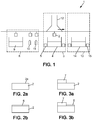
- the figure 1 is a schematic view showing a plant 1 for passivating the surface of a III-V semiconductor material product.
- An example of a product is shown on the figure 2a .
- Product 2 is formed of a III-V semiconductor material. It is manufactured from one or more elements of column "III" of the periodic table of elements (in particular Indium) and from one or more elements of column "V" of the periodic table of elements (in particular antimony or phosphorus).
- the material under consideration is indium phosphide InP.
- Product 2 comprises a surface 2a that one seeks to passivate.
- the installation 21 comprises a passivation apparatus 3.
- This comprises a container 4 containing a liquid solvent.
- the solvent in question consists of NH 3 liquid ammonia.
- the apparatus 3 also comprises temperature control means 5, such as a cryostat, adapted to maintain the ammonia in a liquid state.
- PCl 5 phosphorus pentachloride
- the solvent used is liquid ammonia obtained by a simple expansion in an open glass liquefaction cell maintained at a temperature of -78 ° C. by means of a cooling bath (for example charged acetone). in dry ice) confined in a Dewar vase.
- a cooling bath for example charged acetone
- dry ice confined in a Dewar vase.
- a cryostat thermostated between -40 ° C and -100 ° C, preferably between -50 ° C and -70 ° C or in any other type of refrigerant enclosure providing a maintenance at constant temperature in the range above.
- the liquid ammonia can be taken in neutral form, that is to say in total purity, or acid (introducing for example NH 4 Cl or Br at 0.1 mol / liter of solvent).
- PCl 5 As the oxidizing additive of the III-V semiconductor material, PCl 5 is used. The latter is introduced after weighing, and placed in solution in a standard manner to a level of 1 to 3 millimoles / liter of solvent. If necessary, lower concentrations of PCl5, for example of the order of 0.1 to 1 millimole per liter, may be used. The conditions are met for deposition without electrochemical assistance of a polyphosphazene type P, N polymer film 6 on the surface 2a of the product 2 (cf. Fig. 2b ).
- the assembly generates the continuous paving of the surface 2a, which creates the phenomenon of self-regulation thanks to the limiting factor of the cover.
- This self-regulation maintains, in terms of roughness, a final state very close to the initial state, which excludes disturbances unwanted parasitic morphologies in an optical configuration.
- PCl 5 makes it possible to inject recoverable charge carriers into the surface in order to initiate a mechanism for producing a polyphosphazene type P, N polymer film similar to the mechanism described above in the electrochemical version.
- this component is compatible with liquid ammonia.
- the process is completely implemented without electrochemical assistance (or “electroless”), thus making it possible to create a surface film without implementing complex steps of contact recovery required for known electrochemical assistance processes.
- the method described above is further compatible with typical masking methods used for such components.
- the product 2 carries on the surface a mask 7, for example of the type Si 3 N 4 , SiO 2 , ZnS, or polymer compatible with liquid ammonia.
- the passivation film 6 is formed only on a surface part of the product.
- the mask 7 could be formed of an oxide of the material III-V of the product 2.
- the oxides, in particular of InP or of GaP are perfectly stable in liquid ammonia, even in the presence of PCl 5 .
- the installation 1 may also comprise a deoxidation unit 8 upstream of the passivation apparatus 3 itself.
- the sample 2 is first subjected to the deoxidation process, before being subjected to the formation of the polyphosphazene type film.
- a deoxidation process it is possible, for example, to soak the sample in a deoxidizing solution 9, typically 1M HCl / ultra pure water a few minutes, then rinsing with ultra pure water and drying 11, for example under an argon or nitrogen jet.
- the sample thus conditioned is immediately loaded into the liquid ammonia solution to be passivated.
- the process is thus particularly compatible with the other industrial steps of the manufacture of III-V semiconductor components.
- the sample suspension pod is removed abruptly from the treatment bath 4, simply under a suction hood 12.
- a washing step 13 can then be carried out, for example by immersing the sample in a bath 14.
- ultra pure ammonia This step can last, or even serve for intermediate storage before final extraction.
- the final extraction is done for example by gradual rise in temperature of the sample held in its nacelle via a temperature control device 15.
- the treated sample is then stored in a conventional support for semi-plate. conductive.
- the P, N polymer film obtained without electrochemical assistance by the method described above is different from the polyphosphazene film obtained by the electrochemical assistance processes of the prior art.
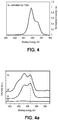
- the XPS photoelectron spectroscopic measurement associated with N 1S has significant differences, as represented on the figure 4 , for the method without electrochemical assistance described above, and on the figure 4a for the previous electrochemical process.
- curve A corresponds to a just deoxidized InP surface
- curve B is obtained after anodic treatment by electrochemical assistance in liquid ammonia and storage in air during at least one year
- the curve B * is obtained by adding an immersion step for 16 hours in an aqueous deoxygenated solution of K 2 PtCl 4 (3 millimoles / liter) after the two steps of the process corresponding to the curve B (this This step induces a reaction of the amine groups of the passivated surface with respect to PtCl 4 2- and acts as a developer (see the publication mentioned below).
- the spectrum in intensity normalized in arbitrary units, has a first peak for a binding energy of about 399 electron volts, and a second peak for a binding energy of about 398 electron volts.
- the amplitude of the first peak (highest binding energy) is much greater than that of the second peak (at least 20% higher), and this very reproducibly.
- peak it is meant that the intensity curve as a function of energy has a maximum between an increasing portion and a decreasing portion.
- the spectrum has two main peaks of similar magnitudes.
- the formed film is very thin and this is demonstrated by the set of XPS data.
- Such an XPS spectrum measurement can thus be considered as a signature of the electrolytic implementation of the polyphosphazene type film formation process.
Landscapes
- Formation Of Insulating Films (AREA)
- Internal Circuitry In Semiconductor Integrated Circuit Devices (AREA)
Description
- La présente invention est relative aux procédés de passivation chimique d'une surface d'un produit de matériau semi-conducteur III-V, et aux produits obtenus par de tels procédés.
- Plus particulièrement, l'invention se rapporte à un procédé de passivation chimique d'une surface d'un produit de matériau semi-conducteur III-V, dans lequel a) on forme un film polymère P,N sur ladite surface par dépôt dans un solvant comprenant de l'ammoniac liquide.
- L'article Gonçalves et al., « Fully Protective yet Functionalizable Monolayer on InP », Chemistry of Materials 22 (2010) 3114-3120 décrit un exemple d'un tel procédé, dans lequel on dépose un film polyphosphazène, et qui donne grande satisfaction. En effet, la passivation de la surface obtenue par ce procédé peut être de grande qualité.
- Ce film est toutefois formé avec une assistance électrochimique, ce qui présente des inconvénients pratiques empêchant de mettre en oeuvre un tel procédé à l'échelle industrielle. On cherche donc à rendre plus simple la production de tels films.
- A cet effet, un procédé du genre en question est caractérisé en ce que ledit film est formé par dépôt sans assistance électrochimique dans ledit solvant, en présence d'un additif chimique à pouvoir oxydant comprenant du phosphore, et générant des porteurs de charge électrique dans ladite surface.
- S'agissant de dépôt « sans assistance électrochimique », on peut aussi parler de dépôt « à potentiel de circuit ouvert ».
- De manière surprenante, on a constaté que l'adjonction d'un tel additif comprenant du phosphore, dans le solvant permettait de mettre en oeuvre la formation d'un film de type polyphosphazène sans assistance électrochimique. On s'affranchit ainsi des opérations complexes nécessaires aux procédés électrochimiques, comme d'avoir à établir une connectique pour la polarisation. De plus, on obtient un film couvrant et ultra-mince.
- Dans des modes de réalisation préférés de l'invention, on peut éventuellement avoir recours en outre à l'une et/ou à l'autre des dispositions suivantes :
- pour l'étape a), on opère par trempage ;
- le matériau « V » est le phosphore ;
- le matériau « III » est l'indium ;
- l'étape a) comprend simultanément une dissolution du matériau semi-conducteur en surface, une oxydation du solvant, et une formation d'un équivalent monomère du polyphosphazène ;
- l'étape a) est mise en oeuvre entre -40°C et -100°C ;
- l'étape a) est mise en oeuvre avec une concentration d'additif comprise entre 0.1 et 3 millimol/l (mM/L) ;
- on met en oeuvre, avant l'étape a), une étape b) de désoxydation d'au moins une partie de ladite surface ;
- l'étape b) est mise en oeuvre pour seulement une partie de la surface ;
- le procédé comprend en outre, après l'étape a), une étape c) de lavage d'une surface passivée à l'étape a) ;
- ledit additif est PCl5.
- Selon un autre aspect, l'invention se rapporte à produit comprenant :
- un substrat de matériau semi-conducteur III-V présentant une surface,
- un film de polymère P,N formé sur ladite surface,
- D'autres caractéristiques et avantages de l'invention apparaîtront au cours de la description suivante d'une de ses formes de réalisation, donnée à titre d'exemple non limitatif, en regard des dessins joints.
- Sur les dessins :
- la
figure 1 est une vue schématique d'une installation pour la mise en oeuvre d'un procédé selon un exemple de réalisation, - la
figure 2a est une vue schématique en coupe d'un produit selon un premier mode de réalisation avant application du procédé, - la
figure 2b est une vue correspondant à lafigure 2a après application du procédé, - les
figures 3a et 3b sont des vues correspondant respectivement auxfigures 2a et 2b pour un produit selon un deuxième mode de réalisation, - la
figure 4 est une courbe représentative de spectrométrie photoélectronique XPS pour N1S pour un produit obtenu par le procédé ci-dessus, et - la
figure 4a est une courbe similaire à la courbe représentée sur lafigure 4 pour des produits obtenus par des procédés avec assistance électrochimique. - Sur les différentes figures, les mêmes références désignent des éléments identiques ou similaires.
- La
figure 1 est une vue schématique représentant une installation 1 de passivation de la surface d'un produit de matériau semi-conducteur III-V. Un exemple de produit est représenté sur lafigure 2a . Le produit 2 est formé d'un matériau semi-conducteur III-V. Il est fabriqué à partir d'un ou plusieurs éléments de la colonne « III » du tableau périodique des éléments (notamment l'Indium) et d'un ou plusieurs éléments de la colonne « V »du tableau périodique des éléments (notamment antimoine ou phosphore). A titre d'exemple, le matériau considéré est le phosphure d'indium InP. Le produit 2 comprend une surface 2a qu'on cherche à passiver. - Comme cela est représenté à la
figure 1 , l'installation 21 comprend un appareil de passivation 3. Celui-ci comprend un récipient 4 contenant un solvant liquide. A titre d'exemple, le solvant en question est constitué d'ammoniac liquide NH3. L'appareil 3 comprend également des moyens de régulation de température 5, tel qu'un cryostat, adapté pour maintenir l'ammoniac en état liquide. - Le produit 2 est placé dans le solvant en présence d'un additif. Cet additif présente un pouvoir oxydant du matériau semi-conducteur III-V dans ledit solvant. On utilise, en particulier, un oxydant :
- qui comprenne du phosphore,
- qui soit compatible avec le solvant ammoniac liquide,
- qui puisse générer des porteurs de charge électrique (trous) dans la surface 2a du produit 2.
- Un exemple particulier d'un tel additif est le pentachlorure de phosphore (PCl5).
- A titre d'exemple, on utilise comme solvant de l'ammoniac liquide obtenu par une simple détente dans une cellule ouverte de liquéfaction en verre maintenue à une température de -78°C grâce à un bain réfrigérant (par exemple de l'acétone chargé en carboglace) confiné dans un vase Dewar. Dans l'alternative, on pourrait également travailler dans un cryostat thermostaté entre -40°C et - 100°C, de préférence entre -50°C et -70°C ou dans tout autre type d'enceinte réfrigérante assurant un maintien à température constante dans la gamme ci-dessus. L'ammoniac liquide peut être pris sous forme neutre, c'est-à-dire en totale pureté, ou acide (en introduisant par exemple NH4Cl ou Br à 0,1 mole/litre de solvant).
- A titre d'additif à pouvoir d'oxydant du matériau semi-conducteur III-V, on utilise PCl5. Ce dernier est introduit après pesée, et mis en solution de façon standard à hauteur de 1 à 3 millimoles/litre de solvant. Le cas échéant, on peut utiliser des concentrations inférieures de PCl5, par exemple de l'ordre de 0,1 à 1 millimole par litre. Les conditions sont réunies pour le dépôt sans assistance électochimique d'un film 6 polymère P,N de type polyphosphazène à la surface 2a du produit 2 (cf.
Fig. 2b ). - De manière générale, le polyphosphazène est un polymère du type (-RR'P=N-)n, où les substituants R,R' sont généralement des alcoxy, des amino, des R2N ou des halogènes.
- Dans le cas présent, on propose que le mécanisme (dans sa version électrochimique) à la base de la réaction puisse s'écrire, dans le cas du phosphure d'indium :

- Cette équation englobe trois phénomènes du mécanisme conduisant à la passivation :
- une dissolution du matériau à l'échelle nanométrique,
- une oxydation du solvant, et
- l'obtention d'un équivalent monomère.
- L'ensemble génère le pavage continu de la surface 2a, qui crée le phénomène d'auto-régulation grâce au facteur limitant de la couverture. Cette auto-régulation maintient, en terme de rugosité, un état final très proche de l'état initial, ce qui exclut des perturbations morphologiques parasites indésirables dans une configuration optique.
- PCl5 permet d'injecter des porteurs de charge récupérables dans la surface, pour engager un mécanisme de production d'un film polymère P,N de type polyphosphazène similaire au mécanisme décrit ci-dessus en version électrochimique. De plus, ce composant est compatible avec l'ammoniac liquide.
- Le procédé est complètement mis en oeuvre sans assistance électrochimique (ou « electroless »), permettant ainsi de créer un film de surface sans mettre en oeuvre des étapes complexes de reprise de contact obligatoires pour des procédés à assistance électrochimique connus.
- Le procédé décrit ci-dessus est de plus compatible avec les procédés de masquage typique utilisés pour des composants de ce type. Comme décrit par exemple sur la
figure 3a , le produit 2 porte en surface un masque 7, par exemple de type Si3N4, SiO2, ZnS, ou polymère compatible avec l'ammoniac liquide. Dans ce cas, comme représenté sur lafigure 3b , le film 6 de passivation est formé uniquement sur une partie de surface du produit. En variante, le masque 7 pourrait être formé d'un oxyde du matériau III-V du produit 2. En effet, les oxydes, en particulier de InP ou de GaP, sont parfaitement stables dans l'ammoniac liquide, même en présence de PCl5. - A titre d'exemple, si on ne souhaite pas qu'un tel oxyde gêne la formation du film 6 de passivation, l'installation 1 peut également comprendre une unité de désoxydation 8 en amont de l'appareil de passivation 3 proprement dit. Ainsi, l'échantillon 2 est d'abord soumis au procédé de désoxydation, avant d'être soumis à la formation du film de type polyphosphazène. A titre d'exemple de procédé de désoxydation, on peut par exemple prévoir de tremper l'échantillon dans une solution désoxydante 9, typiquement HCl 1M/eau ultra pure pendant quelques minutes, puis un rinçage 10 à l'eau ultra pure et un séchage 11, par exemple sous jet d'argon ou d'azote.
- Dans cet exemple de réalisation, l'échantillon ainsi conditionné est immédiatement chargé dans la solution d'ammoniac liquide pour y être passivé.
- Le procédé est ainsi particulièrement compatible avec les autres étapes industrielles de la fabrication de composants semi-conducteurs III-V.
- Après l'étape de formation du film de passivation, on peut également avoir recours à une étape d'extraction. Par exemple, la nacelle de suspension de l'échantillon est retirée brusquement du bain 4 de traitement, simplement sous hotte d'aspiration 12. On peut ensuite procéder à une étape de lavage 13, par exemple en plongeant l'échantillon dans un bain 14 d'ammoniac ultra pur. Cette étape peut durer, voire servir pour un stockage intermédiaire avant extraction définitive. L'extraction définitive se fait par exemple par remontée progressive en température de l'échantillon maintenu dans sa nacelle par l'intermédiaire d'un dispositif de régulation de température 15. L'échantillon traité est ensuite stocké dans un support classique pour plaque semi-conductrice.
- Il a par ailleurs été observé que le film de polymère P,N obtenu sans assistance électrochimique par le procédé décrit ci-dessus, est différent du film polyphosphazène obtenu par les procédés à assistance électrochimiques de l'art antérieur. On peut parler d'un film « de type polyphosphazène », dans la mesure où il présente des caractéristiques proches de films polyphosphazène, sans toutefois être identique. En particulier, la mesure de spectrométrie photoélectronique XPS associée à N1S présente des différences notables, telles que représentées sur la
figure 4 , pour le procédé sans assistance électrochimique décrit ci-dessus, et sur lafigure 4a pour le procédé électrochimique antérieur. Sur lafigure 4a , relative à la réponse N1Δ d'échantillons InP, la courbe A correspond à une surface InP tout juste désoxydée, la courbe B est obtenue après un traitement anodique par assistance électrochimique dans l'ammoniac liquide et un stockage dans l'air pendant au moins un an, et la courbe B* est obtenue en rajoutant une étape d'immersion pendant 16 heures dans une solution désoxygénée aqueuse de K2PtCl4 (3 millimoles/litre) après les deux étapes du procédé correspondant à la courbe B (cette étape induit une réaction des groupes amines de la surface passivée vis-à-vis de PtCl4 2- et agit comme révélateur (cf. la publication mentionnée ci-dessous)). Comme on peut le voir en particulier sur lafigure 4 , en intensité normalisée en unités arbitraires, le spectre présente un premier pic pour une énergie de liaison environ égale à 399 électrons volt, et un deuxième pic pour une énergie de liaison environ égale à 398 électrons volt. L'amplitude du premier pic (énergie de liaison la plus élevée) est nettement supérieure à celle du deuxième pic (au moins 20% supérieure), et ce de manière très reproductible. Ce spectre caractérise bien le film obtenu par le procédé décrit ci-dessus et suggère un grand ordre de surface pour un des environnements chimiques de l'azote dans le film. Par pic, on entend que la courbe d'intensité en fonction de l'énergie présente un maximum entre une partie croissante et une partie décroissante. A titre de comparaison, on notera que, pour les procédés électrolytiques de lafigure 4a , le spectre présente deux pics principaux d'amplitudes semblables. - Par ailleurs, le film formé est très mince et ceci est démontré par l'ensemble des données XPS.
- On peut donc considérer une telle mesure de spectre XPS comme une signature de la mise en oeuvre anélectrolytique du procédé de formation du film de type polyphosphazène.
- La présente description a été donnée principalement en référence au phosphure d'Indium (InP). Il est présumé que les principes à la base de l'invention s'appliquent également aux autres matériaux III-P, toute précaution nécessaire à l'utilisation d'un autre matériau III-P étant prise par ailleurs. En particulier, on présume que la mise en oeuvre du procédé ci-dessus à un matériau de type phosphure de gallium (GaP) est possible.
Claims (12)
- Procédé de passivation chimique d'une surface d'un produit de matériau semi-conducteur III-V, dans lequel a) on forme un film (6) polymère phosphore (P), azote (N) sur ladite surface (2a) par dépôt dans un solvant comprenant de l'ammoniac liquide,
caractérisé en ce que ledit film est formé par dépôt sans assistance électrochimique dans ledit solvant, en présence d'un additif à pouvoir oxydant comprenant du phosphore, et générant des porteurs de charge électrique dans ladite surface. - Procédé selon la revendication 1, dans lequel pour l'étape a), on opère par trempage.
- Procédé selon l'une des revendications 1 à 2, dans lequel le matériau « V » est le phosphore.
- Procédé selon l'une des revendications 1 à 3, dans lequel le matériau « III » est l'indium.
- Procédé selon l'une des revendications 1 à 4, dans lequel l'étape a) comprend simultanément une dissolution du matériau semi-conducteur en surface, une oxydation du solvant, et une formation d'un équivalent monomère du polyphosphazène.
- Procédé selon l'une des revendications 1 à 5, dans lequel l'étape a) est mise en oeuvre entre -40°C et -100°C.
- Procédé selon l'une des revendications 1 à 6, dans lequel l'étape a) est mise en oeuvre avec une concentration d'additif comprise entre 0.1 et 3 millimol/l (mM/L).
- Procédé selon l'une des revendications 1 à 7, dans lequel on met en oeuvre, avant l'étape a), une étape b) de désoxydation d'au moins une partie de ladite surface.
- Procédé selon la revendication 8, dans lequel l'étape b) est mise en oeuvre pour seulement une partie de la surface.
- Procédé selon l'une des revendications 1 à 9, comprenant en outre, après l'étape a), une étape c) de lavage d'une surface passivée à l'étape a).
- Procédé selon l'une des revendications 1 à 10, dans lequel ledit additif est PCl5.
- Produit comprenant :- un substrat (12) de matériau semi-conducteur III-V présentant une surface,- un film (6) de polymère phosphore (P), azote (N) formé sur ladite surface,caractérisé en ce que ledit film présente, en spectrométrie photoélectronique XPS, pour N1S, un spectre présentant un premier pic pour une forte énergie de liaison, et un deuxième pic pour une faible énergie de liaison, le premier pic étant d'amplitude au moins 20% supérieure au deuxième pic.
Applications Claiming Priority (2)
| Application Number | Priority Date | Filing Date | Title |
|---|---|---|---|
| FR1155157A FR2976718B1 (fr) | 2011-06-14 | 2011-06-14 | Procede de passivation chimique d'une surface d'un produit de materiau semi-conducteur iii-v, et produit obtenu par un tel procede |
| PCT/FR2012/051310 WO2012172247A1 (fr) | 2011-06-14 | 2012-06-12 | Procédé de passivation chimique d'une surface d'un produit de matériau semi-conducteur iii-v, et produit obtenu par un tel procédé |
Publications (2)
| Publication Number | Publication Date |
|---|---|
| EP2721634A1 EP2721634A1 (fr) | 2014-04-23 |
| EP2721634B1 true EP2721634B1 (fr) | 2018-01-03 |
Family
ID=46420445
Family Applications (1)
| Application Number | Title | Priority Date | Filing Date |
|---|---|---|---|
| EP12731132.2A Active EP2721634B1 (fr) | 2011-06-14 | 2012-06-12 | Procédé de passivation chimique d'une surface d'un produit de matériau semi-conducteur iii-v, et produit obtenu par un tel procédé |
Country Status (5)
| Country | Link |
|---|---|
| US (1) | US9514961B2 (fr) |
| EP (1) | EP2721634B1 (fr) |
| JP (1) | JP6053765B2 (fr) |
| FR (1) | FR2976718B1 (fr) |
| WO (1) | WO2012172247A1 (fr) |
Families Citing this family (2)
| Publication number | Priority date | Publication date | Assignee | Title |
|---|---|---|---|---|
| JP2508736B2 (ja) | 1987-07-28 | 1996-06-19 | 三菱自動車工業株式会社 | 傾斜型スプリングシ−ト面付き動弁機構 |
| FR3069701B1 (fr) | 2017-07-31 | 2019-12-20 | Centre National De La Recherche Scientifique | Masque perfectionne de protection d'un materiau semiconducteur pour des applications de gravure localisee |
Family Cites Families (18)
| Publication number | Priority date | Publication date | Assignee | Title |
|---|---|---|---|---|
| US4107108A (en) * | 1977-02-08 | 1978-08-15 | Armstrong Cork Company | Polyphosphazene plasticized resins |
| US4789748A (en) * | 1985-10-17 | 1988-12-06 | Allied-Signal, Inc. | Process for preparing electrically conductive poly(isothianaphthene) from 1,3-dihydroisothianaphthene |
| JPS63194339A (ja) * | 1987-02-09 | 1988-08-11 | Nippon Telegr & Teleph Corp <Ntt> | ホスフアゼンおよびホスフアザン化合物の分解による半導体表面保護膜の製造法 |
| JPS6445149A (en) * | 1987-08-13 | 1989-02-17 | Oki Electric Ind Co Ltd | Interlayer insulating film for multilayer interconnection |
| JPH02293471A (ja) * | 1989-04-28 | 1990-12-04 | Nitto Boseki Co Ltd | セルロース系布帛加工剤水溶液の製造方法 |
| US5008169A (en) * | 1989-07-28 | 1991-04-16 | Xerox Corporation | Photoconductive imaging members with polyphosphazenes |
| JP2775117B2 (ja) * | 1990-06-18 | 1998-07-16 | 日本電信電話株式会社 | 保護膜形成方法 |
| JPH0491436A (ja) * | 1990-08-01 | 1992-03-24 | Sumitomo Electric Ind Ltd | Mis構造電極の形成方法 |
| US5266830A (en) * | 1990-08-03 | 1993-11-30 | Sharp Kabushiki Kaisha | Hetero junction bipolar transistor with reduced surface recombination current |
| JP2742340B2 (ja) * | 1990-08-03 | 1998-04-22 | シャープ株式会社 | ヘテロ接合バイポーラトランジスタ |
| JPH05102128A (ja) * | 1991-10-03 | 1993-04-23 | Hitachi Cable Ltd | 化合物半導体結晶ウエハ表面へのAs2S3膜形成方法 |
| JP3555290B2 (ja) * | 1995-12-28 | 2004-08-18 | 東レ株式会社 | ホスファゼン重合体およびその製造方法ならびに成形品およびその製造方法 |
| JPH10106961A (ja) * | 1996-09-30 | 1998-04-24 | Yupiteru Ind Co Ltd | 半導体素子の製造方法 |
| US6284317B1 (en) * | 1998-04-17 | 2001-09-04 | Massachusetts Institute Of Technology | Derivatization of silicon surfaces |
| FR2825513B1 (fr) | 2001-05-31 | 2003-08-29 | Sagem | Procede de traitement par sulfuration de surface semi-conductrice compose iii et v |
| DE102005023728A1 (de) * | 2005-05-23 | 2006-11-30 | Basf Coatings Ag | Lackschichtbildendes Korrosionsschutzmittel und Verfahren zu dessen stromfreier Applikation |
| US8585753B2 (en) * | 2006-03-04 | 2013-11-19 | John James Scanlon | Fibrillated biodegradable prosthesis |
| JP2010533505A (ja) * | 2006-10-10 | 2010-10-28 | セロノバ バイオサイエンシーズ, インコーポレイテッド | シリコーンおよび特定のポリホスファゼンを含む組成物およびデバイス |
-
2011
- 2011-06-14 FR FR1155157A patent/FR2976718B1/fr not_active Expired - Fee Related
-
2012
- 2012-06-12 EP EP12731132.2A patent/EP2721634B1/fr active Active
- 2012-06-12 WO PCT/FR2012/051310 patent/WO2012172247A1/fr not_active Ceased
- 2012-06-12 US US14/126,217 patent/US9514961B2/en active Active
- 2012-06-12 JP JP2014515257A patent/JP6053765B2/ja active Active
Also Published As
| Publication number | Publication date |
|---|---|
| US20150108617A1 (en) | 2015-04-23 |
| JP6053765B2 (ja) | 2016-12-27 |
| FR2976718B1 (fr) | 2013-07-05 |
| FR2976718A1 (fr) | 2012-12-21 |
| EP2721634A1 (fr) | 2014-04-23 |
| WO2012172247A1 (fr) | 2012-12-20 |
| JP2014518449A (ja) | 2014-07-28 |
| US9514961B2 (en) | 2016-12-06 |
Similar Documents
| Publication | Publication Date | Title |
|---|---|---|
| EP3072149B1 (fr) | Procédé de gravure sélective d'un masque disposé sur un substrat silicié | |
| EP2304787B1 (fr) | Traitement de surface par plasma d'azote dans un procédé de collage direct | |
| EP2255029B1 (fr) | Procede de production de nanostructures sur un substrat d'oxyde metallique et dispositif forme de couches minces | |
| EP0847082A2 (fr) | Procédé de traitement d'un substrat semi-conducteur comprenant une étape de traitement de surface | |
| FR2972563A1 (fr) | Procédé de traitement d'une couche de nitrure de métal oxydée | |
| FR3085538A1 (fr) | Tranche soi et son procede de production | |
| EP0265314A1 (fr) | procédé de formation d'une couche isolante comportant du sulfure, dérivés sulfures obtenus et appareillage pour la mise en oeuvre du procédé | |
| WO2012172247A1 (fr) | Procédé de passivation chimique d'une surface d'un produit de matériau semi-conducteur iii-v, et produit obtenu par un tel procédé | |
| EP1030353A1 (fr) | Procédé de gravure anisotrope par plasma gazeux d'un matériau polymère diélectrique organique | |
| WO2002029876A1 (fr) | Procede de revelation de defauts cristallins et/ou de champs de contraintes a l'interface d'adhesion moleculaire de deux materiaux solides | |
| EP1980607B1 (fr) | Solution utilisée dans la fabrication d'un matériau semi-conducteur poreux et procédé de fabrication dudit matériau | |
| EP1473765B1 (fr) | Traitement par brossage d'une plaquette semiconductrice avant collage | |
| EP1328012A1 (fr) | Procédé de fabrication d'un composant électronique incorporant un microcomposantinductif | |
| EP0501862B1 (fr) | Procédé de réalisation d'un laser à semiconducteur à ruban enterré, utilisant une gravure sèche pour former ce ruban et laser obtenu par ce procédé | |
| EP3137656B1 (fr) | Dispositif destine a la mise en oeuvre d'un traitement d'anodisation et traitement d'anodisation | |
| FR2987935A1 (fr) | Procede d'amincissement de la couche active de silicium d'un substrat du type "silicium sur isolant" (soi). | |
| FR3071663A1 (fr) | Procede de fabrication de plaque soi, et plaque soi | |
| WO2000077846A1 (fr) | Procede de fabrication d'un substrat de silicium comportant une mince couche d'oxyde de silicium ensevelie | |
| EP2154712B1 (fr) | Procédé de préparation d'un substrat en ZnO en partie ou en totalité semi-isolant ou dopé de type P, substrats obtenus, et dispositifs électroniques, électrooptiques ou optoélectroniques les comprenant. | |
| EP3503174B1 (fr) | Procede de transfert d'une couche utile | |
| FR2471045A1 (fr) | Procede de preparation de surface d'un corps semi-conducteur pour le depot sur cette surface d'une couche metallique | |
| EP3646371B1 (fr) | Composition chimique de nettoyage pour le retrait d'une couche de passivation amorphe a la surface de materiaux cristallins | |
| FR3069701A1 (fr) | Masque perfectionne de protection d'un materiau semiconducteur pour des applications de gravure localisee | |
| FR2832853A1 (fr) | Procede de fabrication d'un composant electronique incorporant un micro-composant inductif | |
| WO2025141060A1 (fr) | Procédé de collage direct entre deux substrats |
Legal Events
| Date | Code | Title | Description |
|---|---|---|---|
| PUAI | Public reference made under article 153(3) epc to a published international application that has entered the european phase |
Free format text: ORIGINAL CODE: 0009012 |
|
| 17P | Request for examination filed |
Effective date: 20131210 |
|
| AK | Designated contracting states |
Kind code of ref document: A1 Designated state(s): AL AT BE BG CH CY CZ DE DK EE ES FI FR GB GR HR HU IE IS IT LI LT LU LV MC MK MT NL NO PL PT RO RS SE SI SK SM TR |
|
| DAX | Request for extension of the european patent (deleted) | ||
| GRAP | Despatch of communication of intention to grant a patent |
Free format text: ORIGINAL CODE: EPIDOSNIGR1 |
|
| STAA | Information on the status of an ep patent application or granted ep patent |
Free format text: STATUS: GRANT OF PATENT IS INTENDED |
|
| INTG | Intention to grant announced |
Effective date: 20170810 |
|
| GRAS | Grant fee paid |
Free format text: ORIGINAL CODE: EPIDOSNIGR3 |
|
| GRAA | (expected) grant |
Free format text: ORIGINAL CODE: 0009210 |
|
| STAA | Information on the status of an ep patent application or granted ep patent |
Free format text: STATUS: THE PATENT HAS BEEN GRANTED |
|
| AK | Designated contracting states |
Kind code of ref document: B1 Designated state(s): AL AT BE BG CH CY CZ DE DK EE ES FI FR GB GR HR HU IE IS IT LI LT LU LV MC MK MT NL NO PL PT RO RS SE SI SK SM TR |
|
| REG | Reference to a national code |
Ref country code: GB Ref legal event code: FG4D Free format text: NOT ENGLISH |
|
| REG | Reference to a national code |
Ref country code: CH Ref legal event code: EP Ref country code: AT Ref legal event code: REF Ref document number: 961015 Country of ref document: AT Kind code of ref document: T Effective date: 20180115 |
|
| REG | Reference to a national code |
Ref country code: IE Ref legal event code: FG4D Free format text: LANGUAGE OF EP DOCUMENT: FRENCH |
|
| REG | Reference to a national code |
Ref country code: DE Ref legal event code: R096 Ref document number: 602012041582 Country of ref document: DE |
|
| REG | Reference to a national code |
Ref country code: NL Ref legal event code: MP Effective date: 20180103 |
|
| REG | Reference to a national code |
Ref country code: LT Ref legal event code: MG4D |
|
| REG | Reference to a national code |
Ref country code: AT Ref legal event code: MK05 Ref document number: 961015 Country of ref document: AT Kind code of ref document: T Effective date: 20180103 |
|
| REG | Reference to a national code |
Ref country code: FR Ref legal event code: PLFP Year of fee payment: 7 |
|
| PG25 | Lapsed in a contracting state [announced via postgrant information from national office to epo] |
Ref country code: NL Free format text: LAPSE BECAUSE OF FAILURE TO SUBMIT A TRANSLATION OF THE DESCRIPTION OR TO PAY THE FEE WITHIN THE PRESCRIBED TIME-LIMIT Effective date: 20180103 |
|
| PG25 | Lapsed in a contracting state [announced via postgrant information from national office to epo] |
Ref country code: ES Free format text: LAPSE BECAUSE OF FAILURE TO SUBMIT A TRANSLATION OF THE DESCRIPTION OR TO PAY THE FEE WITHIN THE PRESCRIBED TIME-LIMIT Effective date: 20180103 Ref country code: CY Free format text: LAPSE BECAUSE OF FAILURE TO SUBMIT A TRANSLATION OF THE DESCRIPTION OR TO PAY THE FEE WITHIN THE PRESCRIBED TIME-LIMIT Effective date: 20180103 Ref country code: NO Free format text: LAPSE BECAUSE OF FAILURE TO SUBMIT A TRANSLATION OF THE DESCRIPTION OR TO PAY THE FEE WITHIN THE PRESCRIBED TIME-LIMIT Effective date: 20180403 Ref country code: FI Free format text: LAPSE BECAUSE OF FAILURE TO SUBMIT A TRANSLATION OF THE DESCRIPTION OR TO PAY THE FEE WITHIN THE PRESCRIBED TIME-LIMIT Effective date: 20180103 Ref country code: HR Free format text: LAPSE BECAUSE OF FAILURE TO SUBMIT A TRANSLATION OF THE DESCRIPTION OR TO PAY THE FEE WITHIN THE PRESCRIBED TIME-LIMIT Effective date: 20180103 Ref country code: LT Free format text: LAPSE BECAUSE OF FAILURE TO SUBMIT A TRANSLATION OF THE DESCRIPTION OR TO PAY THE FEE WITHIN THE PRESCRIBED TIME-LIMIT Effective date: 20180103 |
|
| PG25 | Lapsed in a contracting state [announced via postgrant information from national office to epo] |
Ref country code: IS Free format text: LAPSE BECAUSE OF FAILURE TO SUBMIT A TRANSLATION OF THE DESCRIPTION OR TO PAY THE FEE WITHIN THE PRESCRIBED TIME-LIMIT Effective date: 20180503 Ref country code: AT Free format text: LAPSE BECAUSE OF FAILURE TO SUBMIT A TRANSLATION OF THE DESCRIPTION OR TO PAY THE FEE WITHIN THE PRESCRIBED TIME-LIMIT Effective date: 20180103 Ref country code: RS Free format text: LAPSE BECAUSE OF FAILURE TO SUBMIT A TRANSLATION OF THE DESCRIPTION OR TO PAY THE FEE WITHIN THE PRESCRIBED TIME-LIMIT Effective date: 20180103 Ref country code: BG Free format text: LAPSE BECAUSE OF FAILURE TO SUBMIT A TRANSLATION OF THE DESCRIPTION OR TO PAY THE FEE WITHIN THE PRESCRIBED TIME-LIMIT Effective date: 20180403 Ref country code: SE Free format text: LAPSE BECAUSE OF FAILURE TO SUBMIT A TRANSLATION OF THE DESCRIPTION OR TO PAY THE FEE WITHIN THE PRESCRIBED TIME-LIMIT Effective date: 20180103 Ref country code: LV Free format text: LAPSE BECAUSE OF FAILURE TO SUBMIT A TRANSLATION OF THE DESCRIPTION OR TO PAY THE FEE WITHIN THE PRESCRIBED TIME-LIMIT Effective date: 20180103 Ref country code: GR Free format text: LAPSE BECAUSE OF FAILURE TO SUBMIT A TRANSLATION OF THE DESCRIPTION OR TO PAY THE FEE WITHIN THE PRESCRIBED TIME-LIMIT Effective date: 20180404 Ref country code: PL Free format text: LAPSE BECAUSE OF FAILURE TO SUBMIT A TRANSLATION OF THE DESCRIPTION OR TO PAY THE FEE WITHIN THE PRESCRIBED TIME-LIMIT Effective date: 20180103 |
|
| PG25 | Lapsed in a contracting state [announced via postgrant information from national office to epo] |
Ref country code: MT Free format text: LAPSE BECAUSE OF FAILURE TO SUBMIT A TRANSLATION OF THE DESCRIPTION OR TO PAY THE FEE WITHIN THE PRESCRIBED TIME-LIMIT Effective date: 20180103 |
|
| REG | Reference to a national code |
Ref country code: DE Ref legal event code: R097 Ref document number: 602012041582 Country of ref document: DE |
|
| PG25 | Lapsed in a contracting state [announced via postgrant information from national office to epo] |
Ref country code: IT Free format text: LAPSE BECAUSE OF FAILURE TO SUBMIT A TRANSLATION OF THE DESCRIPTION OR TO PAY THE FEE WITHIN THE PRESCRIBED TIME-LIMIT Effective date: 20180103 Ref country code: RO Free format text: LAPSE BECAUSE OF FAILURE TO SUBMIT A TRANSLATION OF THE DESCRIPTION OR TO PAY THE FEE WITHIN THE PRESCRIBED TIME-LIMIT Effective date: 20180103 Ref country code: EE Free format text: LAPSE BECAUSE OF FAILURE TO SUBMIT A TRANSLATION OF THE DESCRIPTION OR TO PAY THE FEE WITHIN THE PRESCRIBED TIME-LIMIT Effective date: 20180103 Ref country code: AL Free format text: LAPSE BECAUSE OF FAILURE TO SUBMIT A TRANSLATION OF THE DESCRIPTION OR TO PAY THE FEE WITHIN THE PRESCRIBED TIME-LIMIT Effective date: 20180103 |
|
| PLBE | No opposition filed within time limit |
Free format text: ORIGINAL CODE: 0009261 |
|
| STAA | Information on the status of an ep patent application or granted ep patent |
Free format text: STATUS: NO OPPOSITION FILED WITHIN TIME LIMIT |
|
| PG25 | Lapsed in a contracting state [announced via postgrant information from national office to epo] |
Ref country code: DK Free format text: LAPSE BECAUSE OF FAILURE TO SUBMIT A TRANSLATION OF THE DESCRIPTION OR TO PAY THE FEE WITHIN THE PRESCRIBED TIME-LIMIT Effective date: 20180103 Ref country code: SM Free format text: LAPSE BECAUSE OF FAILURE TO SUBMIT A TRANSLATION OF THE DESCRIPTION OR TO PAY THE FEE WITHIN THE PRESCRIBED TIME-LIMIT Effective date: 20180103 Ref country code: SK Free format text: LAPSE BECAUSE OF FAILURE TO SUBMIT A TRANSLATION OF THE DESCRIPTION OR TO PAY THE FEE WITHIN THE PRESCRIBED TIME-LIMIT Effective date: 20180103 Ref country code: CZ Free format text: LAPSE BECAUSE OF FAILURE TO SUBMIT A TRANSLATION OF THE DESCRIPTION OR TO PAY THE FEE WITHIN THE PRESCRIBED TIME-LIMIT Effective date: 20180103 |
|
| 26N | No opposition filed |
Effective date: 20181005 |
|
| REG | Reference to a national code |
Ref country code: CH Ref legal event code: PL |
|
| PG25 | Lapsed in a contracting state [announced via postgrant information from national office to epo] |
Ref country code: SI Free format text: LAPSE BECAUSE OF FAILURE TO SUBMIT A TRANSLATION OF THE DESCRIPTION OR TO PAY THE FEE WITHIN THE PRESCRIBED TIME-LIMIT Effective date: 20180103 |
|
| REG | Reference to a national code |
Ref country code: BE Ref legal event code: MM Effective date: 20180630 |
|
| REG | Reference to a national code |
Ref country code: IE Ref legal event code: MM4A |
|
| PG25 | Lapsed in a contracting state [announced via postgrant information from national office to epo] |
Ref country code: LU Free format text: LAPSE BECAUSE OF NON-PAYMENT OF DUE FEES Effective date: 20180612 Ref country code: MC Free format text: LAPSE BECAUSE OF FAILURE TO SUBMIT A TRANSLATION OF THE DESCRIPTION OR TO PAY THE FEE WITHIN THE PRESCRIBED TIME-LIMIT Effective date: 20180103 |
|
| PG25 | Lapsed in a contracting state [announced via postgrant information from national office to epo] |
Ref country code: CH Free format text: LAPSE BECAUSE OF NON-PAYMENT OF DUE FEES Effective date: 20180630 Ref country code: IE Free format text: LAPSE BECAUSE OF NON-PAYMENT OF DUE FEES Effective date: 20180612 Ref country code: LI Free format text: LAPSE BECAUSE OF NON-PAYMENT OF DUE FEES Effective date: 20180630 |
|
| PG25 | Lapsed in a contracting state [announced via postgrant information from national office to epo] |
Ref country code: BE Free format text: LAPSE BECAUSE OF NON-PAYMENT OF DUE FEES Effective date: 20180630 |
|
| PG25 | Lapsed in a contracting state [announced via postgrant information from national office to epo] |
Ref country code: TR Free format text: LAPSE BECAUSE OF FAILURE TO SUBMIT A TRANSLATION OF THE DESCRIPTION OR TO PAY THE FEE WITHIN THE PRESCRIBED TIME-LIMIT Effective date: 20180103 |
|
| PG25 | Lapsed in a contracting state [announced via postgrant information from national office to epo] |
Ref country code: PT Free format text: LAPSE BECAUSE OF FAILURE TO SUBMIT A TRANSLATION OF THE DESCRIPTION OR TO PAY THE FEE WITHIN THE PRESCRIBED TIME-LIMIT Effective date: 20180103 Ref country code: HU Free format text: LAPSE BECAUSE OF FAILURE TO SUBMIT A TRANSLATION OF THE DESCRIPTION OR TO PAY THE FEE WITHIN THE PRESCRIBED TIME-LIMIT; INVALID AB INITIO Effective date: 20120612 |
|
| PG25 | Lapsed in a contracting state [announced via postgrant information from national office to epo] |
Ref country code: MK Free format text: LAPSE BECAUSE OF NON-PAYMENT OF DUE FEES Effective date: 20180103 |
|
| PGFP | Annual fee paid to national office [announced via postgrant information from national office to epo] |
Ref country code: GB Payment date: 20250626 Year of fee payment: 14 |
|
| PGFP | Annual fee paid to national office [announced via postgrant information from national office to epo] |
Ref country code: FR Payment date: 20250626 Year of fee payment: 14 |
|
| PGFP | Annual fee paid to national office [announced via postgrant information from national office to epo] |
Ref country code: DE Payment date: 20250725 Year of fee payment: 14 |
|
| REG | Reference to a national code |
Ref country code: DE Ref legal event code: R079 Ref document number: 602012041582 Country of ref document: DE Free format text: PREVIOUS MAIN CLASS: H01L0021306000 Ipc: H10P0050000000 |