EP2720255A1 - Method for manufacturing silicon carbide semiconductor device - Google Patents
Method for manufacturing silicon carbide semiconductor device Download PDFInfo
- Publication number
- EP2720255A1 EP2720255A1 EP12772184.3A EP12772184A EP2720255A1 EP 2720255 A1 EP2720255 A1 EP 2720255A1 EP 12772184 A EP12772184 A EP 12772184A EP 2720255 A1 EP2720255 A1 EP 2720255A1
- Authority
- EP
- European Patent Office
- Prior art keywords
- film
- silicon carbide
- etching
- semiconductor device
- manufacturing
- Prior art date
- Legal status (The legal status is an assumption and is not a legal conclusion. Google has not performed a legal analysis and makes no representation as to the accuracy of the status listed.)
- Withdrawn
Links
Images



Classifications
-
- H—ELECTRICITY
- H10—SEMICONDUCTOR DEVICES; ELECTRIC SOLID-STATE DEVICES NOT OTHERWISE PROVIDED FOR
- H10D—INORGANIC ELECTRIC SEMICONDUCTOR DEVICES
- H10D30/00—Field-effect transistors [FET]
- H10D30/60—Insulated-gate field-effect transistors [IGFET]
- H10D30/64—Double-diffused metal-oxide semiconductor [DMOS] FETs
- H10D30/66—Vertical DMOS [VDMOS] FETs
-
- H—ELECTRICITY
- H10—SEMICONDUCTOR DEVICES; ELECTRIC SOLID-STATE DEVICES NOT OTHERWISE PROVIDED FOR
- H10P—GENERIC PROCESSES OR APPARATUS FOR THE MANUFACTURE OR TREATMENT OF DEVICES COVERED BY CLASS H10
- H10P10/00—Bonding of wafers, substrates or parts of devices
-
- H—ELECTRICITY
- H10—SEMICONDUCTOR DEVICES; ELECTRIC SOLID-STATE DEVICES NOT OTHERWISE PROVIDED FOR
- H10D—INORGANIC ELECTRIC SEMICONDUCTOR DEVICES
- H10D12/00—Bipolar devices controlled by the field effect, e.g. insulated-gate bipolar transistors [IGBT]
- H10D12/01—Manufacture or treatment
- H10D12/031—Manufacture or treatment of IGBTs
-
- H—ELECTRICITY
- H10—SEMICONDUCTOR DEVICES; ELECTRIC SOLID-STATE DEVICES NOT OTHERWISE PROVIDED FOR
- H10D—INORGANIC ELECTRIC SEMICONDUCTOR DEVICES
- H10D30/00—Field-effect transistors [FET]
- H10D30/01—Manufacture or treatment
- H10D30/021—Manufacture or treatment of FETs having insulated gates [IGFET]
- H10D30/028—Manufacture or treatment of FETs having insulated gates [IGFET] of double-diffused metal oxide semiconductor [DMOS] FETs
- H10D30/0291—Manufacture or treatment of FETs having insulated gates [IGFET] of double-diffused metal oxide semiconductor [DMOS] FETs of vertical DMOS [VDMOS] FETs
-
- H—ELECTRICITY
- H10—SEMICONDUCTOR DEVICES; ELECTRIC SOLID-STATE DEVICES NOT OTHERWISE PROVIDED FOR
- H10D—INORGANIC ELECTRIC SEMICONDUCTOR DEVICES
- H10D62/00—Semiconductor bodies, or regions thereof, of devices having potential barriers
- H10D62/80—Semiconductor bodies, or regions thereof, of devices having potential barriers characterised by the materials
- H10D62/83—Semiconductor bodies, or regions thereof, of devices having potential barriers characterised by the materials being Group IV materials, e.g. B-doped Si or undoped Ge
- H10D62/832—Semiconductor bodies, or regions thereof, of devices having potential barriers characterised by the materials being Group IV materials, e.g. B-doped Si or undoped Ge being Group IV materials comprising two or more elements, e.g. SiGe
- H10D62/8325—Silicon carbide
-
- H—ELECTRICITY
- H10—SEMICONDUCTOR DEVICES; ELECTRIC SOLID-STATE DEVICES NOT OTHERWISE PROVIDED FOR
- H10P—GENERIC PROCESSES OR APPARATUS FOR THE MANUFACTURE OR TREATMENT OF DEVICES COVERED BY CLASS H10
- H10P30/00—Ion implantation into wafers, substrates or parts of devices
- H10P30/20—Ion implantation into wafers, substrates or parts of devices into semiconductor materials, e.g. for doping
- H10P30/22—Ion implantation into wafers, substrates or parts of devices into semiconductor materials, e.g. for doping using masks
-
- H—ELECTRICITY
- H10—SEMICONDUCTOR DEVICES; ELECTRIC SOLID-STATE DEVICES NOT OTHERWISE PROVIDED FOR
- H10P—GENERIC PROCESSES OR APPARATUS FOR THE MANUFACTURE OR TREATMENT OF DEVICES COVERED BY CLASS H10
- H10P50/00—Etching of wafers, substrates or parts of devices
- H10P50/20—Dry etching; Plasma etching; Reactive-ion etching
- H10P50/24—Dry etching; Plasma etching; Reactive-ion etching of semiconductor materials
- H10P50/242—Dry etching; Plasma etching; Reactive-ion etching of semiconductor materials of Group IV materials
-
- H—ELECTRICITY
- H10—SEMICONDUCTOR DEVICES; ELECTRIC SOLID-STATE DEVICES NOT OTHERWISE PROVIDED FOR
- H10P—GENERIC PROCESSES OR APPARATUS FOR THE MANUFACTURE OR TREATMENT OF DEVICES COVERED BY CLASS H10
- H10P50/00—Etching of wafers, substrates or parts of devices
- H10P50/20—Dry etching; Plasma etching; Reactive-ion etching
- H10P50/28—Dry etching; Plasma etching; Reactive-ion etching of insulating materials
- H10P50/282—Dry etching; Plasma etching; Reactive-ion etching of insulating materials of inorganic materials
- H10P50/283—Dry etching; Plasma etching; Reactive-ion etching of insulating materials of inorganic materials by chemical means
-
- H—ELECTRICITY
- H10—SEMICONDUCTOR DEVICES; ELECTRIC SOLID-STATE DEVICES NOT OTHERWISE PROVIDED FOR
- H10D—INORGANIC ELECTRIC SEMICONDUCTOR DEVICES
- H10D64/00—Electrodes of devices having potential barriers
- H10D64/60—Electrodes characterised by their materials
- H10D64/66—Electrodes having a conductor capacitively coupled to a semiconductor by an insulator, e.g. MIS electrodes
- H10D64/68—Electrodes having a conductor capacitively coupled to a semiconductor by an insulator, e.g. MIS electrodes characterised by the insulator, e.g. by the gate insulator
- H10D64/693—Electrodes having a conductor capacitively coupled to a semiconductor by an insulator, e.g. MIS electrodes characterised by the insulator, e.g. by the gate insulator the insulator comprising nitrogen, e.g. nitrides, oxynitrides or nitrogen-doped materials
Definitions
- the present invention relates to a method of manufacturing a silicon carbide semiconductor device.
- the step of selectively forming an impurity region in a semiconductor substrate is performed.
- MOSFET Metal Oxide Semiconductor Field Effect Transistor
- the step of partially forming a p-type impurity region in an n-type semiconductor substrate and further partially forming an n-type impurity region in this p-type impurity region is often performed. Namely, impurity regions different in extension from each other are formed. Both of the impurity regions should be formed in a self-aligned manner, in order to suppress variation in characteristics of the MOSFET, in particular, variation in channel length.
- a double diffusion technique with which extension of an impurity region is adjusted by adjusting a degree of progress of impurity diffusion through heat treatment has widely been used.
- a diffusion coefficient of an impurity is small and a region into which ions have been implanted becomes an impurity region substantially as it is through heat treatment. Therefore, it is difficult to employ the double diffusion technique.
- a size of an opening in a mask for ion implantation should be adjusted.
- PTL 1 Japanese Patent Laying-Open No. 2000-22137 (PTL 1), a polycrystalline silicon film or an oxide film formed by oxidizing the same is employed as a mask and different impurity regions are formed by making use of movement of a mask end owing to oxidation or oxide film removal.
- a sidewall of an opening is subjected to thermal oxidation in order to narrow the opening in a mask and the oxide film is removed in order to widen the opening narrowed as such.
- a thermal oxidation step for adjusting the opening in the mask may often be undesirable or difficult.
- a high temperature approximately from 900 to 1200°C required in the thermal oxidation step may give rise to a problem.
- alloying may occur between a metal underlying film and the silicon carbide substrate at a high temperature.
- a rate of oxidation in the thermal oxidation step is not much high, and for example, a rate of steam oxidation is around 15 nm/minute. Therefore, efficiency in semiconductor device production may be low.
- the following method is available as a method of narrowing an opening in a mask.
- a film is formed on a silicon carbide substrate provided with a mask having an opening.
- the opening is narrowed.
- anisotropic etching allows a portion of the film on the sidewall to remain in the opening in the mask, while the remaining portion is removed.
- the opening narrowed by the film can thus be obtained.
- anisotropic etching should be stopped at appropriate timing. If etching is stopped too early, a portion of the film to be removed remains and the remaining portion may interfere ion implantation. If etching is stopped too late, the film does not sufficiently remain on the sidewall and the opening may not sufficiently be narrowed. Therefore, simply by performing this method, it is difficult to accurately form an impurity region.
- the present invention was made in view of the problems above, and an object of the present invention is to provide a method of manufacturing a silicon carbide semiconductor device capable of forming impurity regions in an accurately self-aligned manner.
- a method of manufacturing a silicon carbide semiconductor device has the following steps.
- a mask layer is formed on a silicon carbide substrate.
- the mask layer includes a cover portion covering the silicon carbide substrate and an opening having a sidewall.
- An impurity of a first conductivity type is implanted onto the silicon carbide substrate through the opening in the mask layer.
- a first film made of a first material is formed on the silicon carbide substrate on which the mask layer has been formed.
- the first film includes a first portion arranged on the cover portion, a second portion arranged on the sidewall of the opening, and a third portion arranged on the silicon carbide substrate in the opening.
- a second film made of a second material different from the first material is formed on the silicon carbide substrate on which the mask layer and the first film have been formed.
- the second film includes a portion arranged on each of the first to third portions of the first film.
- Anisotropic etching for removing a portion of the second film arranged on the third portion of the first film is started. It is sensed that etching of the first material is performed during anisotropic etching. Anisotropic etching is stopped after it is sensed that etching of the first material is performed in the step of sensing that etching of the first material is performed.
- An impurity of a second conductivity type is implanted onto the silicon carbide substrate through the opening narrowed by the second portion of the first film and the second film arranged on the second portion after the step of stopping anisotropic etching.
- an end point of anisotropic etching of the second film is detected by sensing that etching of the first film is performed. Since etching of the first film is performed not only in the opening in the mask layer but also on the cover portion of the mask layer, it can accurately be sensed that etching of the first film is performed. Therefore, since anisotropic etching of the second film can accurately be stopped, the second film can accurately remain on the sidewall of the opening. Thus, since the impurity of the second conductivity type is implanted through the accurately narrowed opening, a region of the second conductivity type can accurately be formed in a part of the region into which the impurity of the first conductivity type has been implanted through the opening.
- the mask layer may be made of the second material.
- the method of manufacturing a silicon carbide semiconductor device can further be simplified.
- a third film made of a material different from the first material is formed.
- a fourth film made of the first material is formed on the third film.
- etching of the first material involved with etching of the fourth film is sensed, and thereafter, at a time interval, etching of the first material involved with etching of the first film will be sensed. Namely, prior to sensing of etching of the first film, sensing predicting the same is carried out. Therefore, accuracy in stopping etching can further be enhanced.
- an underlying layer may be formed on the silicon carbide substrate before a mask layer is formed.
- the underlying layer may be made of the first material.
- the method of manufacturing a silicon carbide semiconductor device can further be simplified.
- the underlying layer may be made of a material different from the first material.
- a selective etching ratio between the underlying layer and the first film can be ensured, and hence accuracy in an amount of remaining underlying layer after anisotropic etching can be enhanced. Therefore, variation in implantation of an impurity of the second conductivity type through the underlying layer can be suppressed.
- the first material does not have to contain a metal element.
- the first material may be made of any of a silicon-based material and a carbon-based material.
- the material for the first film can be free from a metal element.
- impurity regions can be formed in an accurately self-aligned manner.
- MOSFET 100 is specifically a vertical DiMOSFET (Double Implanted MOSFET).
- MOSFET 100 has an epitaxial substrate 90, an oxide film 126, a source electrode 111, an upper source electrode 127, a gate electrode 110, and a drain electrode 112.
- Epitaxial substrate 90 has a single crystal substrate 80, a buffer layer 121, a breakdown voltage holding layer 122, a p region 123, and an n + region 124.
- a two-dimensional shape (a shape when viewed from above in Fig. 1 ) of MOSFET 100 is, for example, a rectangle or a square having a side of a length not shorter than 2 mm.
- Single crystal substrate 80 and buffer layer 121 each have an n conductivity type.
- Single crystal substrate 80 is preferably composed of silicon carbide.
- Concentration of an n-type conductive impurity in buffer layer 121 is, for example, 5 ⁇ 10 17 cm -3 .
- buffer layer 121 has a thickness, for example, of 0.5 ⁇ m.
- Breakdown voltage holding layer 122 is formed on buffer layer 121, and it is composed of silicon carbide having an n conductivity type.
- breakdown voltage holding layer 122 has a thickness of 10 ⁇ m and concentration of an n-type conductive impurity is 5 ⁇ 10 15 cm -3 .
- a plurality of p regions 123 having a p conductivity type are formed at a distance from one another.
- n + region 124 is formed to be located inside each p region 123.
- p region 123 has a channel region lying between n + region 124 and breakdown voltage holding layer 122 and covered with gate electrode 110 with oxide film 126 being interposed.
- oxide film 126 is formed on breakdown voltage holding layer 122 exposed between the plurality of p regions 123 at surface S0. Specifically, oxide film 126 is formed to extend from n + region 124 in one p region 123 over p region 123, breakdown voltage holding layer 122 exposed between two p regions 123, and the other p region 123 to n + region 124 in the other p region 123.
- Gate electrode 110 is formed on oxide film 126. Therefore, a portion of oxide film 126 having gate electrode 110 formed thereon has a function as a gate insulating film.
- source electrode 111 is formed on n + region 124. A part of source electrode 111 may be in contact with p region 123. Upper source electrode 127 is formed on source electrode 111.
- epitaxial substrate 90 (silicon carbide substrate) having surface S0 is prepared.
- buffer layer 121 is formed on a main surface of single crystal substrate 80, and breakdown voltage holding layer 122 is formed on buffer layer 121.
- Buffer layer 121 is composed of silicon carbide having an n conductivity type, and it has a thickness, for example, of 0.5 ⁇ m.
- concentration of the conductive impurity in buffer layer 121 is set, for example, to 5 ⁇ 10 17 cm -3 .
- Breakdown voltage holding layer 122 has a thickness, for example, of 10 ⁇ m.
- concentration of the n conductive impurity in breakdown voltage holding layer 122 is set, for example, to 5 ⁇ 10 15 cm -3 .
- an etching stop layer 50 (an underlying layer) is formed on surface SO of epitaxial substrate 90.
- a material for etching stop layer 50 is, for example, silicon nitride (SiN), titanium (Ti), or silicon (Si).
- Etching stop layer 50 has a thickness, for example, not smaller than 50 nm and not greater than 300 nm.
- a mask layer 31 is deposited on epitaxial substrate 90 with etching stop layer 50 being interposed.
- a material for mask layer 31 is any of silicon oxide (SiO 2 ) and polysilicon, and silicon oxide is more preferred.
- a photoresist pattern 40 is formed on mask layer 31 with photolithography.
- mask layer 31 is patterned through anisotropic etching E1 using photoresist pattern 40 as a mask.
- Anisotropic etching E1 is specifically dry etching, and for example, it is reactive ion etching or ion milling. Then, remaining photoresist pattern 40 is removed.
- mask layer 31 having an opening is formed on epitaxial substrate 90 with etching stop layer 50 being interposed.
- mask layer 31 has a cover portion CV covering epitaxial substrate 90 with etching stop layer 50 being interposed and an opening OP having a sidewall S1.
- an area of opening OP is normally smaller than an area of cover portion CV.
- a ratio of the area of opening OP to the total area of cover portion CV and opening OP is preferably not higher than 5% and more preferably not higher than 3%, in terms of dimension specifications of MOSFET 100 ( Fig. 1 ).
- a p-type (the first conductivity type) impurity is implanted onto epitaxial substrate 90.
- p region 123 is formed from surface SO to a prescribed depth in epitaxial substrate 90.
- an end point film 32 (a first film) is formed on epitaxial substrate 90 on which etching stop layer 50 and mask layer 31 have been formed.
- End point film 32 has portions P1 to P3.
- Portion P1 (a first portion) is arranged on cover portion CV
- portion P2 (a second portion) is arranged on sidewall S1 of opening OP
- portion P3 (a third portion) is arranged on epitaxial substrate 90 in opening OP, with etching stop layer 50 being interposed.
- a material (a first material) for end point film 32 preferably does not substantially contain a metal element, and it is, for example, a silicon-based material or a carbon-based material.
- the silicon-based material is, for example, silicon nitride (SiN).
- the carbon-based material is, for example, carbon (C).
- a material for end point film 32 may be the same as a material for etching stop layer 50. In contrast, a material for end point film 32 may be different from a material for etching stop layer 50.
- a spacer film 33 (a second film) is formed on epitaxial substrate 90 on which mask layer 31 and end point film 32 have been formed.
- Spacer film 33 includes a portion arranged on each of portions P1 to P3 of end point film 32.
- Spacer film 33 is formed, for example, with p-CVD (plasma-Chemical Vapor Deposition).
- p-CVD plasma-Chemical Vapor Deposition
- a film formation temperature is around 400°C and a rate of film formation is from 50 to 300 nm/minute.
- Spacer film 33 is made of a material (a second material) different from the material (the first material) for end point film 32.
- a material for each of end point film 32 and spacer film 33 is selected such that atoms of at least one type are contained in only one of spacer film 33 and end point film 32.
- a material for spacer film 33 is, for example, silicon oxide (SiO 2 ).
- a material for spacer film 33 is the same as a material for mask layer 31.
- anisotropic etching for removing a portion of spacer film 33 that is arranged on portions P1 and P3 of end point film 32 is started.
- Anisotropic etching is dry etching, and for example, it is reactive ion etching or ion milling.
- an end point for identifying a type of a material being etched is started.
- An end point is detected, for example, based on spectroscopic analysis of light emitted during etching or mass spectrometry of atoms emitted by etching.
- anisotropic etching E2 proceeds, portions P1 and P3 of end point film 32 are exposed. Accordingly, the material for end point film 32 starts to be etched. Namely, etching of the material different from the material for spacer film 33 is started. Therefore, exposure of a part of end point film 32 is sensed in end point detection. In the present embodiment, etching by a prescribed amount is further performed after exposure of end point film 32 was sensed. In other words, overetching is performed, so that portions P1 and P3 are removed. Thereafter, anisotropic etching E2 is stopped. It is noted that this overetching may not be performed.
- a composite mask 30 having mask layer 31, end point film 32, and spacer film 33 is formed on epitaxial substrate 90 with etching stop layer 50 being interposed.
- n + region 124 is formed from surface SO to a prescribed depth in epitaxial substrate 90.
- composite mask 30 and etching stop layer 50 are removed.
- activation heat treatment is performed. This heat treatment is performed, for example, by performing heating at 1700°C in an argon atmosphere for 30 minutes.
- oxide film 126 to serve as a gate insulating film is formed on epitaxial substrate 90. Specifically, oxide film 126 is formed to cover breakdown voltage holding layer 122, p region 123, and n + region 124. Formation may be carried out by dry oxidation (thermal oxidation). Conditions in dry oxidation are, for example, a heating temperature of 1200°C and a heating time period of 30 minutes.
- a nitriding heat treatment step is performed.
- This heat treatment is performed, for example, by performing heating in a nitrogen monoxide (NO) atmosphere at 1100°C for 120 minutes. Consequently, nitrogen atoms are introduced in the vicinity of an interface between each of breakdown voltage holding layer 122, p region 123 and n + region 124 and oxide film 126.
- NO nitrogen monoxide
- heat treatment using an argon (Ar) gas which is an inert gas may further be performed.
- Conditions in this heat treatment are, for example, a heating temperature of 1100°C and a heating time period of 60 minutes.
- source electrode 111 is formed. Specifically, the following step is performed.
- a resist film having a pattern is formed on oxide film 126 with photolithography. Using this resist film as a mask, a portion of oxide film 126 located on n + region 124 is etched away. Thus, an opening is formed in oxide film 126. Then, a conductor film is formed in this opening to be in contact with n + region 124. Then, by removing the resist film, a portion of the conductor film above that has been located on the resist film is removed (lift-off).
- This conductor film may be a metal film and it is composed, for example, of nickel (Ni). As a result of this lift-off, source electrode 111 is formed.
- heat treatment for alloying is preferably performed here. For example, heat treatment for 2 minutes at a heating temperature of 950°C in an atmosphere of an argon (Ar) gas which is an inert gas is performed.
- Ar argon
- upper source electrode 127 is formed on source electrode 111.
- gate electrode 110 is formed on oxide film 126.
- drain electrode 112 is formed on a back surface (a lower surface in the drawing) of single crystal substrate 80.
- MOSFET 100 is obtained as described above.
- spacer film 33 is formed without end point film 32 being provided ( Fig. 17 ). It is assumed that mask layer 31 and the spacer film are made of silicon oxide and etching stop layer 50 is made of titanium. Thereafter, anisotropic etching as in the present embodiment is performed. As etching of spacer film 33 proceeds, an upper surface of mask layer 31 and etching stop layer 50 in opening OP are exposed ( Fig. 18 ). Here, since both of the material for spacer film 33 and the material for mask layer 31 are silicon oxide, exposure of the upper surface of mask layer 31 cannot be an object to be detected as an end point.
- an object to be detected as an end point is only exposure of etching stop layer 50 in opening OP.
- Variation in intensity I in end point detection that is, lowering in O (oxygen) atom intensity or increase in Ti (titanium) atom intensity, can theoretically be detected.
- Such variation in intensity originates from difference in material exposed through opening OP. Therefore, as a ratio of an area of opening OP occupied in mask layer 31 is lower, variation in intensity is less. As thus variation in intensity is less, end point detection is actually difficult.
- end point film 32 ( Fig. 10 ) being provided as in the present embodiment, for example in a case where end point film 32 is made of silicon nitride, exposure of portion P1 of end point film 32 at the upper surface of mask layer 31 leads to abrupt increase in nitrogen (N) atom intensity ( Fig. 20 ). Therefore, since end point detection is easy, etching can accurately be stopped.
- an end point of anisotropic etching of spacer film 33 is detected based on sensing of etching of end point film 32 ( Fig. 11 ) being performed. Since etching of end point film 32 is performed not only in opening OP ( Fig. 9 ) in mask layer 31 but also on cover portion CV ( Fig. 9 ) of mask layer 31, it can accurately be sensed that etching of end point film 32 is performed. As anisotropic etching of spacer film 33 can thus accurately be stopped, spacer film 33 can accurately remain on sidewall S1 of opening OP. Therefore, since ion implantation J2 ( Fig.
- an n-type region can accurately be formed in a part of the region into which a p-type impurity has been implanted (p region 123) through opening OP.
- etching stop layer 50 is formed ( Fig. 3 )
- overetching of epitaxial substrate 90 can be suppressed ( Figs. 11 and 12 ).
- the material for mask layer 31 is the same as the material for spacer film 33, and in this case, the method of manufacturing MOSFET 100 can further be simplified.
- the material for etching stop layer 50 may be the same as the material for end point film 32, and in this case, the method of manufacturing MOSFET 100 can further be simplified. Alternatively, they may be different from each other, and in this case, a selective etching ratio between etching stop layer 50 and end point film 32 can be ensured. Therefore, accuracy in an amount of remaining etching stop layer 50 ( Fig. 12 ) after anisotropic etching ( Fig. 11 ) can be enhanced. Therefore, variation in implantation of an n-type impurity through etching stop layer 50 can be suppressed.
- a material for end point film 32 does not contain a metal element, so that metal contamination of an apparatus for manufacturing MOSFET 100 can be avoided.
- an intermediate film 34 (a third film) made of a material different from the material for end point film 32 is formed.
- An intermediate film 35 (a fourth film) made of a material the same as the material for end point film 32 is formed on intermediate film 34.
- Spacer film 33 is formed on intermediate film 35.
- a material for intermediate film 34 is the same as at least any of a material for mask layer 31 and a material for spacer film 33.
- MOSFET 100 ( Fig. 1 ) is obtained through steps substantially similar to those in Figs. 11 to 18 (the first embodiment).
- etching of a material for intermediate film 35 is sensed, and thereafter, at a time interval, etching of the same material involved with etching of end point film 32 will be sensed. Namely, prior to sensing of etching of end point film 32, etching of intermediate film 35, which predicts the same, is sensed. Therefore, accuracy in stopping etching can further be enhanced.
- a material for each of mask layer 31, intermediate film 34, and spacer film 33 is silicon oxide
- a material for each of end point film 32 and intermediate film 35 is silicon nitride
- a material for etching stop layer 50 is titanium
- variation in intensity I as shown in Fig. 22 is sensed. Specifically, prior to final increase in N (nitrogen) atom intensity, peak of N atom intensity is detected.
- etching stop layer 50 is exposed at the time of ion implantation J2 ( Fig. 13 ) in each embodiment above, this is not essential and end point film 32 may remain on etching stop layer 50.
- ion implantation J2 does not necessary have to be performed through etching stop layer 50 and etching stop layer 50 does not have to be formed.
- the p-type is defined as the first conductivity type and the n-type is defined as the second conductivity type
- the n-type may be defined as the first conductivity type and the p-type may be defined as the second conductivity type.
- a conductivity type is selected such that a semiconductor device has an n-type channel.
- a semiconductor device may be a MISFET (Metal Insulator Semiconductor Field Effect Transistor) other than the MOSFET.
- a semiconductor device may be other than a MISFET and it may be, for example, an IGBT (Insulated Gate Bipolar Transistor).
Landscapes
- Electrodes Of Semiconductors (AREA)
- Drying Of Semiconductors (AREA)
Abstract
An impurity of a first conductivity type is implanted onto a silicon carbide substrate (90) through an opening (OP) in a mask layer (31). First and second films (32, 33) made of first and second materials respectively are formed. It is sensed that etching of the first material is performed during anisotropic etching, and then anisotropic etching is stopped. An impurity of a second conductivity type is implanted onto the silicon carbide substrate (90) through the opening (OP) narrowed by the first and second films (32, 33). Thus, the impurity regions can be formed in an accurately self-aligned manner.
Description
- The present invention relates to a method of manufacturing a silicon carbide semiconductor device.
- In manufacturing a semiconductor device, the step of selectively forming an impurity region in a semiconductor substrate is performed. For example, in manufacturing an n-channel type MOSFET (Metal Oxide Semiconductor Field Effect Transistor), in order to obtain an npn structure, the step of partially forming a p-type impurity region in an n-type semiconductor substrate and further partially forming an n-type impurity region in this p-type impurity region is often performed. Namely, impurity regions different in extension from each other are formed. Both of the impurity regions should be formed in a self-aligned manner, in order to suppress variation in characteristics of the MOSFET, in particular, variation in channel length. In a case where a silicon substrate is employed as a semiconductor substrate, a double diffusion technique with which extension of an impurity region is adjusted by adjusting a degree of progress of impurity diffusion through heat treatment has widely been used.
- In a case where a silicon carbide substrate is employed as a semiconductor substrate, however, a diffusion coefficient of an impurity is small and a region into which ions have been implanted becomes an impurity region substantially as it is through heat treatment. Therefore, it is difficult to employ the double diffusion technique. Thus, in order to obtain impurity regions formed in a self-aligned manner, a size of an opening in a mask for ion implantation should be adjusted. For example, according to Japanese Patent Laying-Open No.
2000-22137 - PTL 1: Japanese Patent Laying-Open No.
2000-22137 - According to the technique described in the literature above, a sidewall of an opening is subjected to thermal oxidation in order to narrow the opening in a mask and the oxide film is removed in order to widen the opening narrowed as such. A thermal oxidation step for adjusting the opening in the mask, however, may often be undesirable or difficult. Specifically, a high temperature approximately from 900 to 1200°C required in the thermal oxidation step may give rise to a problem. For example, in a case where a metal underlying layer is formed on a silicon carbide substrate, alloying may occur between a metal underlying film and the silicon carbide substrate at a high temperature. In addition, a rate of oxidation in the thermal oxidation step is not much high, and for example, a rate of steam oxidation is around 15 nm/minute. Therefore, efficiency in semiconductor device production may be low.
- Then, the following method is available as a method of narrowing an opening in a mask. Initially, a film is formed on a silicon carbide substrate provided with a mask having an opening. As the film is formed on a sidewall of the opening, the opening is narrowed. Then, anisotropic etching allows a portion of the film on the sidewall to remain in the opening in the mask, while the remaining portion is removed. The opening narrowed by the film can thus be obtained. With this method, however, anisotropic etching should be stopped at appropriate timing. If etching is stopped too early, a portion of the film to be removed remains and the remaining portion may interfere ion implantation. If etching is stopped too late, the film does not sufficiently remain on the sidewall and the opening may not sufficiently be narrowed. Therefore, simply by performing this method, it is difficult to accurately form an impurity region.
- The present invention was made in view of the problems above, and an object of the present invention is to provide a method of manufacturing a silicon carbide semiconductor device capable of forming impurity regions in an accurately self-aligned manner.
- A method of manufacturing a silicon carbide semiconductor device according to the present invention has the following steps. A mask layer is formed on a silicon carbide substrate. The mask layer includes a cover portion covering the silicon carbide substrate and an opening having a sidewall. An impurity of a first conductivity type is implanted onto the silicon carbide substrate through the opening in the mask layer. A first film made of a first material is formed on the silicon carbide substrate on which the mask layer has been formed. The first film includes a first portion arranged on the cover portion, a second portion arranged on the sidewall of the opening, and a third portion arranged on the silicon carbide substrate in the opening. A second film made of a second material different from the first material is formed on the silicon carbide substrate on which the mask layer and the first film have been formed. The second film includes a portion arranged on each of the first to third portions of the first film. Anisotropic etching for removing a portion of the second film arranged on the third portion of the first film is started. It is sensed that etching of the first material is performed during anisotropic etching. Anisotropic etching is stopped after it is sensed that etching of the first material is performed in the step of sensing that etching of the first material is performed. An impurity of a second conductivity type is implanted onto the silicon carbide substrate through the opening narrowed by the second portion of the first film and the second film arranged on the second portion after the step of stopping anisotropic etching.
- According to the present invention, an end point of anisotropic etching of the second film is detected by sensing that etching of the first film is performed. Since etching of the first film is performed not only in the opening in the mask layer but also on the cover portion of the mask layer, it can accurately be sensed that etching of the first film is performed. Therefore, since anisotropic etching of the second film can accurately be stopped, the second film can accurately remain on the sidewall of the opening. Thus, since the impurity of the second conductivity type is implanted through the accurately narrowed opening, a region of the second conductivity type can accurately be formed in a part of the region into which the impurity of the first conductivity type has been implanted through the opening.
- In the manufacturing method above, the mask layer may be made of the second material.
- Since the material for the mask layer is thus the same as the material for the second film, the method of manufacturing a silicon carbide semiconductor device can further be simplified.
- In the manufacturing method above, after a first film is formed and before a second film is formed, the following steps may be performed. A third film made of a material different from the first material is formed. A fourth film made of the first material is formed on the third film.
- In this case, as etching proceeds, etching of the first material involved with etching of the fourth film is sensed, and thereafter, at a time interval, etching of the first material involved with etching of the first film will be sensed. Namely, prior to sensing of etching of the first film, sensing predicting the same is carried out. Therefore, accuracy in stopping etching can further be enhanced.
- In the manufacturing method above, an underlying layer may be formed on the silicon carbide substrate before a mask layer is formed.
- Thus, overetching of the silicon carbide substrate can be suppressed.
- In the manufacturing method above, the underlying layer may be made of the first material.
- Thus, since the material for the underlying layer is the same as the material for the first film, the method of manufacturing a silicon carbide semiconductor device can further be simplified.
- In the manufacturing method above, the underlying layer may be made of a material different from the first material.
- Thus, a selective etching ratio between the underlying layer and the first film can be ensured, and hence accuracy in an amount of remaining underlying layer after anisotropic etching can be enhanced. Therefore, variation in implantation of an impurity of the second conductivity type through the underlying layer can be suppressed.
- In the manufacturing method above, the first material does not have to contain a metal element.
- Thus, metal contamination of an apparatus for manufacturing a silicon carbide semiconductor device can be avoided.
- In the manufacturing method above, the first material may be made of any of a silicon-based material and a carbon-based material.
- Thus, the material for the first film can be free from a metal element.
- As is clear from the description above, according to the present invention, impurity regions can be formed in an accurately self-aligned manner.
-
-
Fig. 1 is a partial cross-sectional view schematically showing a construction of a silicon carbide semiconductor device in a first embodiment of the present invention. -
Fig. 2 is a partial cross-sectional view schematically showing a first step in a method of manufacturing a silicon carbide semiconductor device inFig. 1 . -
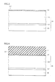
Fig. 3 is a partial cross-sectional view schematically showing a second step in the method of manufacturing a silicon carbide semiconductor device inFig. 1 . -
Fig. 4 is a partial cross-sectional view schematically showing a third step in the method of manufacturing a silicon carbide semiconductor device inFig. 1 . -
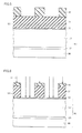
Fig. 5 is a partial cross-sectional view schematically showing a fourth step in the method of manufacturing a silicon carbide semiconductor device inFig. 1 . -
Fig. 6 is a partial cross-sectional view schematically showing a fifth step in the method of manufacturing a silicon carbide semiconductor device inFig. 1 . -
Fig. 7 is a partial cross-sectional view schematically showing a sixth step in the method of manufacturing a silicon carbide semiconductor device inFig. 1 . -
Fig. 8 is a partial cross-sectional view schematically showing a seventh step in the method of manufacturing a silicon carbide semiconductor device inFig. 1 . -
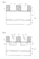
Fig. 9 is a partial cross-sectional view schematically showing an eighth step in the method of manufacturing a silicon carbide semiconductor device inFig. 1 . -
Fig. 10 is a partial cross-sectional view schematically showing a ninth step in the method of manufacturing a silicon carbide semiconductor device inFig. 1 . -
Fig. 11 is a partial cross-sectional view schematically showing a tenth step in the method of manufacturing a silicon carbide semiconductor device inFig. 1 . -
Fig. 12 is a partial cross-sectional view schematically showing an eleventh step in the method of manufacturing a silicon carbide semiconductor device inFig. 1 . -
Fig. 13 is a partial cross-sectional view schematically showing a twelfth step in the method of manufacturing a silicon carbide semiconductor device inFig. 1 . -
Fig. 14 is a partial cross-sectional view schematically showing a thirteenth step in the method of manufacturing a silicon carbide semiconductor device inFig. 1 . -
Fig. 15 is a partial cross-sectional view schematically showing a fourteenth step in the method of manufacturing a silicon carbide semiconductor device inFig. 1 . -
Fig. 16 is a partial cross-sectional view schematically showing a fifteenth step in the method of manufacturing a silicon carbide semiconductor device inFig. 1 . -
Fig. 17 is a cross-sectional view schematically showing a first step in a manufacturing method in a comparative example. -
Fig. 18 is a cross-sectional view schematically showing a second step in the manufacturing method in the comparative example. -
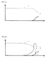
Fig. 19 is a graph showing one example of how an end point is detected in the comparative example. -
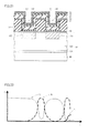
Fig. 20 is a graph showing one example of how an end point is detected in the first embodiment of the present invention. -
Fig. 21 is a partial cross-sectional view schematically showing one step in a method of manufacturing a silicon carbide semiconductor device in a second embodiment of the present invention. -
Fig. 22 is a graph showing one example of how an end point is detected in the second embodiment of the present invention. - An embodiment of the present invention will be described hereinafter with reference to the drawings.
- Initially, a structure of a
MOSFET 100 representing a silicon carbide semiconductor device in the present embodiment will be described with reference toFig. 1 .MOSFET 100 is specifically a vertical DiMOSFET (Double Implanted MOSFET).MOSFET 100 has anepitaxial substrate 90, anoxide film 126, asource electrode 111, anupper source electrode 127, agate electrode 110, and adrain electrode 112.Epitaxial substrate 90 has asingle crystal substrate 80, abuffer layer 121, a breakdownvoltage holding layer 122,a p region 123, and an n+ region 124. A two-dimensional shape (a shape when viewed from above inFig. 1 ) ofMOSFET 100 is, for example, a rectangle or a square having a side of a length not shorter than 2 mm. -
Single crystal substrate 80 andbuffer layer 121 each have an n conductivity type.Single crystal substrate 80 is preferably composed of silicon carbide. Concentration of an n-type conductive impurity inbuffer layer 121 is, for example, 5×1017 cm-3. In addition,buffer layer 121 has a thickness, for example, of 0.5 µm. - Breakdown
voltage holding layer 122 is formed onbuffer layer 121, and it is composed of silicon carbide having an n conductivity type. For example, breakdownvoltage holding layer 122 has a thickness of 10 µm and concentration of an n-type conductive impurity is 5×1015 cm-3. - In a surface SO of
epitaxial substrate 90, a plurality ofp regions 123 having a p conductivity type are formed at a distance from one another. In addition, in surface S0, n+ region 124 is formed to be located inside eachp region 123. In surface S0,p region 123 has a channel region lying between n+ region 124 and breakdownvoltage holding layer 122 and covered withgate electrode 110 withoxide film 126 being interposed. - On breakdown
voltage holding layer 122 exposed between the plurality ofp regions 123 at surface S0,oxide film 126 is formed. Specifically,oxide film 126 is formed to extend from n+ region 124 in onep region 123 overp region 123, breakdownvoltage holding layer 122 exposed between twop regions 123, and theother p region 123 to n+ region 124 in theother p region 123.Gate electrode 110 is formed onoxide film 126. Therefore, a portion ofoxide film 126 havinggate electrode 110 formed thereon has a function as a gate insulating film. In addition,source electrode 111 is formed on n+ region 124. A part ofsource electrode 111 may be in contact withp region 123.Upper source electrode 127 is formed onsource electrode 111. - A method of
manufacturing MOSFET 100 will now be described below. - As shown in
Fig. 2 , epitaxial substrate 90 (silicon carbide substrate) having surface S0 is prepared. Specifically,buffer layer 121 is formed on a main surface ofsingle crystal substrate 80, and breakdownvoltage holding layer 122 is formed onbuffer layer 121.Buffer layer 121 is composed of silicon carbide having an n conductivity type, and it has a thickness, for example, of 0.5 µm. In addition, concentration of the conductive impurity inbuffer layer 121 is set, for example, to 5×1017 cm-3. Breakdownvoltage holding layer 122 has a thickness, for example, of 10 µm. Further, concentration of the n conductive impurity in breakdownvoltage holding layer 122 is set, for example, to 5×1015 cm-3. - As shown in
Fig. 3 , in the present embodiment, an etching stop layer 50 (an underlying layer) is formed on surface SO ofepitaxial substrate 90. A material foretching stop layer 50 is, for example, silicon nitride (SiN), titanium (Ti), or silicon (Si).Etching stop layer 50 has a thickness, for example, not smaller than 50 nm and not greater than 300 nm. - As shown in
Fig. 4 , amask layer 31 is deposited onepitaxial substrate 90 withetching stop layer 50 being interposed. Preferably, a material formask layer 31 is any of silicon oxide (SiO2) and polysilicon, and silicon oxide is more preferred. - As shown in
Fig. 5 , aphotoresist pattern 40 is formed onmask layer 31 with photolithography. - As shown in
Fig. 6 ,mask layer 31 is patterned through anisotropic etching E1 usingphotoresist pattern 40 as a mask. Anisotropic etching E1 is specifically dry etching, and for example, it is reactive ion etching or ion milling. Then, remainingphotoresist pattern 40 is removed. - As shown in
Fig. 7 , as a result of the steps so far,mask layer 31 having an opening is formed onepitaxial substrate 90 withetching stop layer 50 being interposed. Specifically,mask layer 31 has a cover portion CV coveringepitaxial substrate 90 withetching stop layer 50 being interposed and an opening OP having a sidewall S1. In terms of dimension specifications of MOSFET 100 (Fig. 1 ), in a plan view, an area of opening OP is normally smaller than an area of cover portion CV. Specifically, a ratio of the area of opening OP to the total area of cover portion CV and opening OP (that is, an area of mask layer 31) is preferably not higher than 5% and more preferably not higher than 3%, in terms of dimension specifications of MOSFET 100 (Fig. 1 ). - As shown in
Fig. 8 , as a result of ion implantation J1 through opening OP inmask layer 31, a p-type (the first conductivity type) impurity is implanted ontoepitaxial substrate 90. Thus,p region 123 is formed from surface SO to a prescribed depth inepitaxial substrate 90. - As shown in
Fig. 9 , thereafter, an end point film 32 (a first film) is formed onepitaxial substrate 90 on whichetching stop layer 50 andmask layer 31 have been formed.End point film 32 has portions P1 to P3. Portion P1 (a first portion) is arranged on cover portion CV, portion P2 (a second portion) is arranged on sidewall S1 of opening OP, and portion P3 (a third portion) is arranged onepitaxial substrate 90 in opening OP, withetching stop layer 50 being interposed. A material (a first material) forend point film 32 preferably does not substantially contain a metal element, and it is, for example, a silicon-based material or a carbon-based material. The silicon-based material is, for example, silicon nitride (SiN). The carbon-based material is, for example, carbon (C). In addition, a material forend point film 32 may be the same as a material foretching stop layer 50. In contrast, a material forend point film 32 may be different from a material foretching stop layer 50. - As shown in
Fig. 10 , a spacer film 33 (a second film) is formed onepitaxial substrate 90 on whichmask layer 31 andend point film 32 have been formed.Spacer film 33 includes a portion arranged on each of portions P1 to P3 ofend point film 32.Spacer film 33 is formed, for example, with p-CVD (plasma-Chemical Vapor Deposition). In p-CVD, for example, a film formation temperature is around 400°C and a rate of film formation is from 50 to 300 nm/minute. -
Spacer film 33 is made of a material (a second material) different from the material (the first material) forend point film 32. Preferably, a material for each ofend point film 32 andspacer film 33 is selected such that atoms of at least one type are contained in only one ofspacer film 33 andend point film 32. A material forspacer film 33 is, for example, silicon oxide (SiO2). Preferably, a material forspacer film 33 is the same as a material formask layer 31. - Then, anisotropic etching for removing a portion of
spacer film 33 that is arranged on portions P1 and P3 ofend point film 32 is started. Anisotropic etching is dry etching, and for example, it is reactive ion etching or ion milling. - In addition, detection of an end point for identifying a type of a material being etched is started. An end point is detected, for example, based on spectroscopic analysis of light emitted during etching or mass spectrometry of atoms emitted by etching.
- As shown in
Fig. 11 , as anisotropic etching E2 proceeds, portions P1 and P3 ofend point film 32 are exposed. Accordingly, the material forend point film 32 starts to be etched. Namely, etching of the material different from the material forspacer film 33 is started. Therefore, exposure of a part ofend point film 32 is sensed in end point detection. In the present embodiment, etching by a prescribed amount is further performed after exposure ofend point film 32 was sensed. In other words, overetching is performed, so that portions P1 and P3 are removed. Thereafter, anisotropic etching E2 is stopped. It is noted that this overetching may not be performed. - As shown in
Fig. 12 , as a result of etching described above, a composite mask 30 havingmask layer 31,end point film 32, andspacer film 33 is formed onepitaxial substrate 90 withetching stop layer 50 being interposed. - As shown in
Fig. 13 , as a result of ion implantation J2 through opening OP narrowed by portion P2 ofend point film 32 andspacer film 33 arranged on portion P2, an n-type (the second conductivity type) impurity is implanted ontoepitaxial substrate 90. Thus, n+ region 124 is formed from surface SO to a prescribed depth inepitaxial substrate 90. - As further shown in
Fig. 14 , composite mask 30 andetching stop layer 50 are removed. In addition, activation heat treatment is performed. This heat treatment is performed, for example, by performing heating at 1700°C in an argon atmosphere for 30 minutes. - As shown in
Fig. 15 ,oxide film 126 to serve as a gate insulating film is formed onepitaxial substrate 90. Specifically,oxide film 126 is formed to cover breakdownvoltage holding layer 122,p region 123, and n+ region 124. Formation may be carried out by dry oxidation (thermal oxidation). Conditions in dry oxidation are, for example, a heating temperature of 1200°C and a heating time period of 30 minutes. - Thereafter, a nitriding heat treatment step is performed. This heat treatment is performed, for example, by performing heating in a nitrogen monoxide (NO) atmosphere at 1100°C for 120 minutes. Consequently, nitrogen atoms are introduced in the vicinity of an interface between each of breakdown
voltage holding layer 122,p region 123 and n+ region 124 andoxide film 126. It is noted that, after this heat treatment step using nitrogen monoxide, heat treatment using an argon (Ar) gas which is an inert gas may further be performed. Conditions in this heat treatment are, for example, a heating temperature of 1100°C and a heating time period of 60 minutes. - As shown in
Fig. 16 ,source electrode 111 is formed. Specifically, the following step is performed. - A resist film having a pattern is formed on
oxide film 126 with photolithography. Using this resist film as a mask, a portion ofoxide film 126 located on n+ region 124 is etched away. Thus, an opening is formed inoxide film 126. Then, a conductor film is formed in this opening to be in contact with n+ region 124. Then, by removing the resist film, a portion of the conductor film above that has been located on the resist film is removed (lift-off). This conductor film may be a metal film and it is composed, for example, of nickel (Ni). As a result of this lift-off,source electrode 111 is formed. - It is noted that heat treatment for alloying is preferably performed here. For example, heat treatment for 2 minutes at a heating temperature of 950°C in an atmosphere of an argon (Ar) gas which is an inert gas is performed.
- Referring again to
Fig. 1 ,upper source electrode 127 is formed onsource electrode 111. In addition,gate electrode 110 is formed onoxide film 126. Moreover,drain electrode 112 is formed on a back surface (a lower surface in the drawing) ofsingle crystal substrate 80.MOSFET 100 is obtained as described above. - A comparative example will now be described. In the comparative example, unlike the present embodiment (
Fig. 10 ),spacer film 33 is formed withoutend point film 32 being provided (Fig. 17 ). It is assumed thatmask layer 31 and the spacer film are made of silicon oxide andetching stop layer 50 is made of titanium. Thereafter, anisotropic etching as in the present embodiment is performed. As etching ofspacer film 33 proceeds, an upper surface ofmask layer 31 andetching stop layer 50 in opening OP are exposed (Fig. 18 ). Here, since both of the material forspacer film 33 and the material formask layer 31 are silicon oxide, exposure of the upper surface ofmask layer 31 cannot be an object to be detected as an end point. Therefore, an object to be detected as an end point is only exposure ofetching stop layer 50 in opening OP. Variation in intensity I in end point detection (Fig. 19 ), that is, lowering in O (oxygen) atom intensity or increase in Ti (titanium) atom intensity, can theoretically be detected. Such variation in intensity, however, originates from difference in material exposed through opening OP. Therefore, as a ratio of an area of opening OP occupied inmask layer 31 is lower, variation in intensity is less. As thus variation in intensity is less, end point detection is actually difficult. - In contrast, with end point film 32 (
Fig. 10 ) being provided as in the present embodiment, for example in a case whereend point film 32 is made of silicon nitride, exposure of portion P1 ofend point film 32 at the upper surface ofmask layer 31 leads to abrupt increase in nitrogen (N) atom intensity (Fig. 20 ). Therefore, since end point detection is easy, etching can accurately be stopped. - More generally discussing this aspect, according to the present embodiment, an end point of anisotropic etching of
spacer film 33 is detected based on sensing of etching of end point film 32 (Fig. 11 ) being performed. Since etching ofend point film 32 is performed not only in opening OP (Fig. 9 ) inmask layer 31 but also on cover portion CV (Fig. 9 ) ofmask layer 31, it can accurately be sensed that etching ofend point film 32 is performed. As anisotropic etching ofspacer film 33 can thus accurately be stopped,spacer film 33 can accurately remain on sidewall S1 of opening OP. Therefore, since ion implantation J2 (Fig. 13 ) of the n-type impurity is carried out through accurately narrowed opening OP, an n-type region can accurately be formed in a part of the region into which a p-type impurity has been implanted (p region 123) through opening OP. - In addition, as
etching stop layer 50 is formed (Fig. 3 ), overetching ofepitaxial substrate 90 can be suppressed (Figs. 11 and 12 ). - Preferably, the material for
mask layer 31 is the same as the material forspacer film 33, and in this case, the method ofmanufacturing MOSFET 100 can further be simplified. - The material for
etching stop layer 50 may be the same as the material forend point film 32, and in this case, the method ofmanufacturing MOSFET 100 can further be simplified. Alternatively, they may be different from each other, and in this case, a selective etching ratio betweenetching stop layer 50 andend point film 32 can be ensured. Therefore, accuracy in an amount of remaining etching stop layer 50 (Fig. 12 ) after anisotropic etching (Fig. 11 ) can be enhanced. Therefore, variation in implantation of an n-type impurity throughetching stop layer 50 can be suppressed. - Preferably, a material for
end point film 32 does not contain a metal element, so that metal contamination of an apparatus formanufacturing MOSFET 100 can be avoided. - In the present embodiment as well, initially, steps substantially similar to those in
Figs. 2 to 9 (the first embodiment) are performed. - As shown in
Fig. 21 , then, an intermediate film 34 (a third film) made of a material different from the material forend point film 32 is formed. An intermediate film 35 (a fourth film) made of a material the same as the material forend point film 32 is formed onintermediate film 34.Spacer film 33 is formed onintermediate film 35. Preferably, a material forintermediate film 34 is the same as at least any of a material formask layer 31 and a material forspacer film 33. - Then, MOSFET 100 (
Fig. 1 ) is obtained through steps substantially similar to those inFigs. 11 to 18 (the first embodiment). - Since a construction other than the above is substantially the same as the construction in the first embodiment described above, the same or corresponding elements have the same reference characters allotted and description thereof will not be repeated.
- According to the present embodiment, as etching proceeds, etching of a material for
intermediate film 35 is sensed, and thereafter, at a time interval, etching of the same material involved with etching ofend point film 32 will be sensed. Namely, prior to sensing of etching ofend point film 32, etching ofintermediate film 35, which predicts the same, is sensed. Therefore, accuracy in stopping etching can further be enhanced. For example, in a case where a material for each ofmask layer 31,intermediate film 34, andspacer film 33 is silicon oxide, a material for each ofend point film 32 andintermediate film 35 is silicon nitride, and a material foretching stop layer 50 is titanium, variation in intensity I as shown inFig. 22 is sensed. Specifically, prior to final increase in N (nitrogen) atom intensity, peak of N atom intensity is detected. - Though etching
stop layer 50 is exposed at the time of ion implantation J2 (Fig. 13 ) in each embodiment above, this is not essential andend point film 32 may remain onetching stop layer 50. In addition, ion implantation J2 does not necessary have to be performed throughetching stop layer 50 andetching stop layer 50 does not have to be formed. - In addition, though the p-type is defined as the first conductivity type and the n-type is defined as the second conductivity type, the n-type may be defined as the first conductivity type and the p-type may be defined as the second conductivity type. Preferably, a conductivity type is selected such that a semiconductor device has an n-type channel.
- Further, though a MOSFET has been described in detail, a semiconductor device may be a MISFET (Metal Insulator Semiconductor Field Effect Transistor) other than the MOSFET. Furthermore, a semiconductor device may be other than a MISFET and it may be, for example, an IGBT (Insulated Gate Bipolar Transistor).
- It should be understood that the embodiments disclosed herein are illustrative and non-restrictive in every respect. The scope of the present invention is defined by the terms of the claims, rather than the description above, and is intended to include any modifications within the scope and meaning equivalent to the terms of the claims.
- 30 composite mask; 31 mask layer; 32 end point film (first film); 33 spacer film (second film); 34 intermediate film (third film); 35 intermediate film (fourth film); 50 etching stop layer (underlying layer); 80 single crystal substrate; 90 epitaxial substrate (silicon carbide substrate); CV cover portion; and OP opening.
Claims (8)
- A method of manufacturing a silicon carbide semiconductor device (100), comprising the steps of:forming a mask layer (31) on a silicon carbide substrate (90), said mask layer including a cover portion (CV) covering said silicon carbide substrate and an opening (OP) having a sidewall (S1);implanting an impurity of a first conductivity type onto said silicon carbide substrate through said opening in said mask layer;forming a first film (32) made of a first material on said silicon carbide substrate on which said mask layer has been formed, said first film including a first portion (P1) arranged on said cover portion, a second portion (P2) arranged on said sidewall of said opening, and a third portion (P3) arranged on said silicon carbide substrate in said opening;forming a second film (33) made of a second material different from said first material, on said silicon carbide substrate on which said mask layer and said first film have been formed, said second film including a portion arranged on each of said first to third portions of said first film;starting anisotropic etching for removing a portion of said second film arranged on said third portion of said first film;sensing that etching of said first material is performed during said anisotropic etching;stopping said anisotropic etching after it is sensed that etching of said first material is performed in the step of sensing that etching of said first material is performed; andimplanting an impurity of a second conductivity type onto said silicon carbide substrate through said opening narrowed by said second portion of said first film and said second film arranged on said second portion after said step of stopping said anisotropic etching.
- The method of manufacturing a silicon carbide semiconductor device according to claim 1, wherein
said mask layer is made of said second material. - The method of manufacturing a silicon carbide semiconductor device according to claim 1, further comprising, after said step of forming a first film and before said step of forming a second film, the steps of:forming a third film (34) made of a material different from said first material; andforming a fourth film (35) made of said first material on said third film.
- The method of manufacturing a silicon carbide semiconductor device according to claim 1, further comprising the step of forming an underlying layer (50) on said silicon carbide substrate before said step of forming a mask layer.
- The method of manufacturing a silicon carbide semiconductor device according to claim 4, wherein
said underlying layer is made of said first material. - The method of manufacturing a silicon carbide semiconductor device according to claim 4, wherein
said underlying layer is made of a material different from said first material. - The method of manufacturing a silicon carbide semiconductor device according to claim 1, wherein
said first material does not contain a metal element. - The method of manufacturing a silicon carbide semiconductor device according to claim 7, wherein
said first material is made of any of a silicon-based material and a carbon-based material.
Applications Claiming Priority (2)
| Application Number | Priority Date | Filing Date | Title |
|---|---|---|---|
| JP2011126886A JP2012253291A (en) | 2011-06-07 | 2011-06-07 | Method of manufacturing silicon carbide semiconductor device |
| PCT/JP2012/052073 WO2012169218A1 (en) | 2011-06-07 | 2012-01-31 | Method for manufacturing silicon carbide semiconductor device |
Publications (1)
| Publication Number | Publication Date |
|---|---|
| EP2720255A1 true EP2720255A1 (en) | 2014-04-16 |
Family
ID=47293540
Family Applications (1)
| Application Number | Title | Priority Date | Filing Date |
|---|---|---|---|
| EP12772184.3A Withdrawn EP2720255A1 (en) | 2011-06-07 | 2012-01-31 | Method for manufacturing silicon carbide semiconductor device |
Country Status (8)
| Country | Link |
|---|---|
| US (1) | US8796123B2 (en) |
| EP (1) | EP2720255A1 (en) |
| JP (1) | JP2012253291A (en) |
| KR (1) | KR20140024790A (en) |
| CN (1) | CN102959694A (en) |
| CA (1) | CA2793467A1 (en) |
| TW (1) | TW201251024A (en) |
| WO (1) | WO2012169218A1 (en) |
Families Citing this family (4)
| Publication number | Priority date | Publication date | Assignee | Title |
|---|---|---|---|---|
| JP2014175470A (en) | 2013-03-08 | 2014-09-22 | Sumitomo Electric Ind Ltd | Silicon carbide semiconductor device manufacturing method |
| US10937869B2 (en) | 2018-09-28 | 2021-03-02 | General Electric Company | Systems and methods of masking during high-energy implantation when fabricating wide band gap semiconductor devices |
| KR102699369B1 (en) * | 2022-06-14 | 2024-08-26 | 재단법인부산테크노파크 | A method of forming a junction structure using self-aligne contact of silicon carbide MOSFET power semiconductor |
| CN121772724A (en) * | 2026-03-03 | 2026-03-31 | 合肥晶合集成电路股份有限公司 | Method for manufacturing semiconductor device and semiconductor device |
Family Cites Families (10)
| Publication number | Priority date | Publication date | Assignee | Title |
|---|---|---|---|---|
| JP2809662B2 (en) * | 1989-01-24 | 1998-10-15 | 沖電気工業株式会社 | Method for manufacturing double-diffused MOSFET device |
| JP3113425B2 (en) * | 1992-11-27 | 2000-11-27 | 三洋電機株式会社 | Insulated gate semiconductor device and method of manufacturing the same |
| JP3371708B2 (en) * | 1996-08-22 | 2003-01-27 | ソニー株式会社 | Manufacturing method of vertical field effect transistor |
| JP3460585B2 (en) | 1998-07-07 | 2003-10-27 | 富士電機株式会社 | Method for manufacturing silicon carbide MOS semiconductor device |
| US7045845B2 (en) * | 2002-08-16 | 2006-05-16 | Semiconductor Components Industries, L.L.C. | Self-aligned vertical gate semiconductor device |
| JP3997886B2 (en) * | 2002-10-22 | 2007-10-24 | 日産自動車株式会社 | Method for manufacturing silicon carbide semiconductor device |
| JP2004349329A (en) * | 2003-05-20 | 2004-12-09 | Sanyo Electric Co Ltd | Method for manufacturing insulated gate type semiconductor device |
| JP5504597B2 (en) * | 2007-12-11 | 2014-05-28 | 住友電気工業株式会社 | Silicon carbide semiconductor device and manufacturing method thereof |
| CN102017159B (en) * | 2008-09-12 | 2013-06-12 | 住友电气工业株式会社 | Silicon carbide semiconductor device and process for producing the silicon carbide semiconductor device |
| US7868379B2 (en) * | 2008-12-17 | 2011-01-11 | Semiconductor Components Industries, Llc | Electronic device including a trench and a conductive structure therein |
-
2011
- 2011-06-07 JP JP2011126886A patent/JP2012253291A/en active Pending
-
2012
- 2012-01-31 KR KR1020127026956A patent/KR20140024790A/en not_active Withdrawn
- 2012-01-31 CA CA2793467A patent/CA2793467A1/en not_active Abandoned
- 2012-01-31 EP EP12772184.3A patent/EP2720255A1/en not_active Withdrawn
- 2012-01-31 CN CN2012800011861A patent/CN102959694A/en active Pending
- 2012-01-31 WO PCT/JP2012/052073 patent/WO2012169218A1/en not_active Ceased
- 2012-04-12 TW TW101113066A patent/TW201251024A/en unknown
- 2012-06-05 US US13/489,152 patent/US8796123B2/en active Active
Non-Patent Citations (1)
| Title |
|---|
| See references of WO2012169218A1 * |
Also Published As
| Publication number | Publication date |
|---|---|
| KR20140024790A (en) | 2014-03-03 |
| JP2012253291A (en) | 2012-12-20 |
| CN102959694A (en) | 2013-03-06 |
| WO2012169218A1 (en) | 2012-12-13 |
| CA2793467A1 (en) | 2012-12-07 |
| TW201251024A (en) | 2012-12-16 |
| US20120315746A1 (en) | 2012-12-13 |
| US8796123B2 (en) | 2014-08-05 |
Similar Documents
| Publication | Publication Date | Title |
|---|---|---|
| JP5845714B2 (en) | Method for manufacturing silicon carbide semiconductor device | |
| US8642436B2 (en) | Method of manufacturing silicon carbide semiconductor device | |
| JP5525940B2 (en) | Semiconductor device and manufacturing method of semiconductor device | |
| JP5577478B1 (en) | Semiconductor device | |
| CN102844871B (en) | Semiconductor device and manufacturing method therefor | |
| TW201216409A (en) | Process for production of semiconductor device | |
| CN103477439A (en) | Semiconductor device and process for production thereof | |
| KR101171586B1 (en) | Semiconductor device and manufacturing method therefor | |
| JP5329835B2 (en) | Manufacturing method of semiconductor device | |
| JP2006066439A (en) | Semiconductor device and manufacturing method thereof | |
| CA2792551A1 (en) | Method for manufacturing silicon carbide semiconductor device | |
| WO2014073127A1 (en) | Semiconductor device and production method for same | |
| JP5834801B2 (en) | Semiconductor device manufacturing method and semiconductor device | |
| US20260026064A1 (en) | Silicon carbide semiconductor device | |
| US8796123B2 (en) | Method of manufacturing silicon carbide semiconductor device | |
| JP5526493B2 (en) | Trench gate type semiconductor device and manufacturing method thereof | |
| JP2009004804A (en) | Semiconductor device | |
| JP2006303272A (en) | Semiconductor device and manufacturing method thereof | |
| WO2014102916A1 (en) | Silicon carbide semiconductor device | |
| JP2016004955A (en) | Silicon carbide semiconductor device and manufacturing method of the same | |
| JP2006313937A (en) | Semiconductor device |
Legal Events
| Date | Code | Title | Description |
|---|---|---|---|
| PUAI | Public reference made under article 153(3) epc to a published international application that has entered the european phase |
Free format text: ORIGINAL CODE: 0009012 |
|
| 17P | Request for examination filed |
Effective date: 20121023 |
|
| AK | Designated contracting states |
Kind code of ref document: A1 Designated state(s): AL AT BE BG CH CY CZ DE DK EE ES FI FR GB GR HR HU IE IS IT LI LT LU LV MC MK MT NL NO PL PT RO RS SE SI SK SM TR |
|
| DAX | Request for extension of the european patent (deleted) | ||
| STAA | Information on the status of an ep patent application or granted ep patent |
Free format text: STATUS: THE APPLICATION HAS BEEN WITHDRAWN |
|
| 18W | Application withdrawn |
Effective date: 20141029 |