EP2717658A1 - Wiring board and method for manufacturing wiring board - Google Patents
Wiring board and method for manufacturing wiring board Download PDFInfo
- Publication number
- EP2717658A1 EP2717658A1 EP12789574.6A EP12789574A EP2717658A1 EP 2717658 A1 EP2717658 A1 EP 2717658A1 EP 12789574 A EP12789574 A EP 12789574A EP 2717658 A1 EP2717658 A1 EP 2717658A1
- Authority
- EP
- European Patent Office
- Prior art keywords
- hole
- metal plate
- base
- joined
- bent portion
- Prior art date
- Legal status (The legal status is an assumption and is not a legal conclusion. Google has not performed a legal analysis and makes no representation as to the accuracy of the status listed.)
- Granted
Links
Images









Classifications
-
- H—ELECTRICITY
- H05—ELECTRIC TECHNIQUES NOT OTHERWISE PROVIDED FOR
- H05K—PRINTED CIRCUITS; CASINGS OR CONSTRUCTIONAL DETAILS OF ELECTRIC APPARATUS; MANUFACTURE OF ASSEMBLAGES OF ELECTRICAL COMPONENTS
- H05K1/00—Printed circuits
- H05K1/02—Details
- H05K1/11—Printed elements for providing electric connections to or between printed circuits
-
- H—ELECTRICITY
- H05—ELECTRIC TECHNIQUES NOT OTHERWISE PROVIDED FOR
- H05K—PRINTED CIRCUITS; CASINGS OR CONSTRUCTIONAL DETAILS OF ELECTRIC APPARATUS; MANUFACTURE OF ASSEMBLAGES OF ELECTRICAL COMPONENTS
- H05K3/00—Apparatus or processes for manufacturing printed circuits
- H05K3/0094—Filling or covering plated through-holes or blind plated vias, e.g. for masking or for mechanical reinforcement
-
- H—ELECTRICITY
- H05—ELECTRIC TECHNIQUES NOT OTHERWISE PROVIDED FOR
- H05K—PRINTED CIRCUITS; CASINGS OR CONSTRUCTIONAL DETAILS OF ELECTRIC APPARATUS; MANUFACTURE OF ASSEMBLAGES OF ELECTRICAL COMPONENTS
- H05K3/00—Apparatus or processes for manufacturing printed circuits
- H05K3/40—Forming printed elements for providing electric connections to or between printed circuits
-
- H—ELECTRICITY
- H05—ELECTRIC TECHNIQUES NOT OTHERWISE PROVIDED FOR
- H05K—PRINTED CIRCUITS; CASINGS OR CONSTRUCTIONAL DETAILS OF ELECTRIC APPARATUS; MANUFACTURE OF ASSEMBLAGES OF ELECTRICAL COMPONENTS
- H05K3/00—Apparatus or processes for manufacturing printed circuits
- H05K3/40—Forming printed elements for providing electric connections to or between printed circuits
- H05K3/4038—Through-connections; Vertical interconnect access [VIA] connections
- H05K3/4084—Through-connections; Vertical interconnect access [VIA] connections by deforming at least one of the conductive layers
-
- H—ELECTRICITY
- H05—ELECTRIC TECHNIQUES NOT OTHERWISE PROVIDED FOR
- H05K—PRINTED CIRCUITS; CASINGS OR CONSTRUCTIONAL DETAILS OF ELECTRIC APPARATUS; MANUFACTURE OF ASSEMBLAGES OF ELECTRICAL COMPONENTS
- H05K1/00—Printed circuits
- H05K1/02—Details
- H05K1/0213—Electrical arrangements not otherwise provided for
- H05K1/0263—High current adaptations, e.g. printed high current conductors or using auxiliary non-printed means; Fine and coarse circuit patterns on one circuit board
-
- H—ELECTRICITY
- H05—ELECTRIC TECHNIQUES NOT OTHERWISE PROVIDED FOR
- H05K—PRINTED CIRCUITS; CASINGS OR CONSTRUCTIONAL DETAILS OF ELECTRIC APPARATUS; MANUFACTURE OF ASSEMBLAGES OF ELECTRICAL COMPONENTS
- H05K1/00—Printed circuits
- H05K1/02—Details
- H05K1/11—Printed elements for providing electric connections to or between printed circuits
- H05K1/115—Via connections; Lands around holes or via connections
-
- H—ELECTRICITY
- H05—ELECTRIC TECHNIQUES NOT OTHERWISE PROVIDED FOR
- H05K—PRINTED CIRCUITS; CASINGS OR CONSTRUCTIONAL DETAILS OF ELECTRIC APPARATUS; MANUFACTURE OF ASSEMBLAGES OF ELECTRICAL COMPONENTS
- H05K2201/00—Indexing scheme relating to printed circuits covered by H05K1/00
- H05K2201/03—Conductive materials
- H05K2201/0302—Properties and characteristics in general
- H05K2201/0305—Solder used for other purposes than connections between PCB or components, e.g. for filling vias or for programmable patterns
-
- H—ELECTRICITY
- H05—ELECTRIC TECHNIQUES NOT OTHERWISE PROVIDED FOR
- H05K—PRINTED CIRCUITS; CASINGS OR CONSTRUCTIONAL DETAILS OF ELECTRIC APPARATUS; MANUFACTURE OF ASSEMBLAGES OF ELECTRICAL COMPONENTS
- H05K2201/00—Indexing scheme relating to printed circuits covered by H05K1/00
- H05K2201/09—Shape and layout
- H05K2201/09209—Shape and layout details of conductors
- H05K2201/095—Conductive through-holes or vias
- H05K2201/09509—Blind vias, i.e. vias having one side closed
-
- H—ELECTRICITY
- H05—ELECTRIC TECHNIQUES NOT OTHERWISE PROVIDED FOR
- H05K—PRINTED CIRCUITS; CASINGS OR CONSTRUCTIONAL DETAILS OF ELECTRIC APPARATUS; MANUFACTURE OF ASSEMBLAGES OF ELECTRICAL COMPONENTS
- H05K2201/00—Indexing scheme relating to printed circuits covered by H05K1/00
- H05K2201/09—Shape and layout
- H05K2201/09209—Shape and layout details of conductors
- H05K2201/09654—Shape and layout details of conductors covering at least two types of conductors provided for in H05K2201/09218 - H05K2201/095
- H05K2201/0969—Apertured conductors
-
- H—ELECTRICITY
- H05—ELECTRIC TECHNIQUES NOT OTHERWISE PROVIDED FOR
- H05K—PRINTED CIRCUITS; CASINGS OR CONSTRUCTIONAL DETAILS OF ELECTRIC APPARATUS; MANUFACTURE OF ASSEMBLAGES OF ELECTRICAL COMPONENTS
- H05K2203/00—Indexing scheme relating to apparatus or processes for manufacturing printed circuits covered by H05K3/00
- H05K2203/03—Metal processing
- H05K2203/033—Punching metal foil, e.g. solder foil
-
- H—ELECTRICITY
- H05—ELECTRIC TECHNIQUES NOT OTHERWISE PROVIDED FOR
- H05K—PRINTED CIRCUITS; CASINGS OR CONSTRUCTIONAL DETAILS OF ELECTRIC APPARATUS; MANUFACTURE OF ASSEMBLAGES OF ELECTRICAL COMPONENTS
- H05K2203/00—Indexing scheme relating to apparatus or processes for manufacturing printed circuits covered by H05K3/00
- H05K2203/11—Treatments characterised by their effect, e.g. heating, cooling, roughening
- H05K2203/1178—Means for venting or for letting gases escape
-
- H—ELECTRICITY
- H05—ELECTRIC TECHNIQUES NOT OTHERWISE PROVIDED FOR
- H05K—PRINTED CIRCUITS; CASINGS OR CONSTRUCTIONAL DETAILS OF ELECTRIC APPARATUS; MANUFACTURE OF ASSEMBLAGES OF ELECTRICAL COMPONENTS
- H05K3/00—Apparatus or processes for manufacturing printed circuits
- H05K3/40—Forming printed elements for providing electric connections to or between printed circuits
- H05K3/4038—Through-connections; Vertical interconnect access [VIA] connections
-
- H—ELECTRICITY
- H05—ELECTRIC TECHNIQUES NOT OTHERWISE PROVIDED FOR
- H05K—PRINTED CIRCUITS; CASINGS OR CONSTRUCTIONAL DETAILS OF ELECTRIC APPARATUS; MANUFACTURE OF ASSEMBLAGES OF ELECTRICAL COMPONENTS
- H05K3/00—Apparatus or processes for manufacturing printed circuits
- H05K3/40—Forming printed elements for providing electric connections to or between printed circuits
- H05K3/4038—Through-connections; Vertical interconnect access [VIA] connections
- H05K3/4046—Through-connections; Vertical interconnect access [VIA] connections using auxiliary conductive elements, e.g. metallic spheres, eyelets, pieces of wire
-
- Y—GENERAL TAGGING OF NEW TECHNOLOGICAL DEVELOPMENTS; GENERAL TAGGING OF CROSS-SECTIONAL TECHNOLOGIES SPANNING OVER SEVERAL SECTIONS OF THE IPC; TECHNICAL SUBJECTS COVERED BY FORMER USPC CROSS-REFERENCE ART COLLECTIONS [XRACs] AND DIGESTS
- Y10—TECHNICAL SUBJECTS COVERED BY FORMER USPC
- Y10T—TECHNICAL SUBJECTS COVERED BY FORMER US CLASSIFICATION
- Y10T29/00—Metal working
- Y10T29/49—Method of mechanical manufacture
- Y10T29/49002—Electrical device making
- Y10T29/49117—Conductor or circuit manufacturing
- Y10T29/49124—On flat or curved insulated base, e.g., printed circuit, etc.
- Y10T29/49155—Manufacturing circuit on or in base
- Y10T29/49165—Manufacturing circuit on or in base by forming conductive walled aperture in base
Definitions
- the present invention relates to a wiring board and a method for manufacturing a wiring board.
- interlayer connection is achieved in a substrate by performing copper plating.
- a surface layer 301 e.g., copper foil
- a surface layer 302 e.g., copper foil
- a large current e.g. 120 amperes
- Patent document 1 discloses technology that allows for the flow of a large current. More specifically, in a printed wiring board, current through holes, which extend from a front side to a rear side of a substrate, are arranged in a concentrated manner. This allows for the flow of a large current of 50 to 180 amperes without using a bus bar.
- a large current e.g., 120 amperes
- a copper plating layer 305 having an increased thickness may be formed by extending the plating time. However, this would raise the surface of the substrate by ⁇ H. In a subsequent process, this would cause difficulties when mounting electronic components and when applying solder.
- a first aspect of the present invention is a wiring board provided with a base including a front surface, a rear surface, and a side surface.
- a first metal plate is joined with the front surface.
- a second metal plate is joined with the rear surface.
- a conductive line is configured to electrically connect the first metal plate and the second metal plate.
- the conductive line is arranged in an inner space defined by an inner wall surface of a base through hole formed in the base or an outer space located at an outer side of the side surface of the base.
- the conductive line includes the first metal plate, the second metal plate, and a conductive material electrically connecting the first metal plate and the second metal plate.
- At least one of the first metal plate and the second metal plate includes a joined portion, which is joined with the base, and a bent portion, which is bent and extended from the joined portion to cover the inner wall surface or the side surface.
- the conductive material fills an inner side of the bent portion.
- At least one of the first metal plate and the second metal plate includes a joined portion, which is joined with the base, and a bent portion, which is bent and extended from the joined portion to cover the inner wall surface or the side surface.
- the conductive material fills an inner side of the bent portion.
- the conductive line includes the first metal plate, which is joined with the front surface, the second metal plate, which is joined with the rear surface, and the conductive line, which electrically connects the first metal plate and the second metal plate.
- the conductive line electrically connects the first metal plate and the second metal plate in an inner space of a base through hole extending through the base or an outer space located at an outer side of the side surface of the base. This allows for a large current to flow through the conductive line connecting the first metal plate and the second metal plate. Further, the conductive material is filled in the space having a reduced size. This decreases the amount of the filled constructive material.
- the first metal plate includes a first joined portion, which serves as the joined portion, and a first bent portion, which serves as the bent portion.
- the first bent portion is bent toward the rear surface.
- the second metal plate includes a second joined portion, which serves as the joined portion, and a second bent portion, which serves as the bent portion.
- the second bent portion is bent toward the front surface to cover the inner wall surface or the side surface together with the first bent portion.
- the conductive material is filled between the first bent portion and the second bent portion.
- the above structure allows for a large current to flow through the conductive line connecting the first metal plate and the second metal plate.
- the portion where the conductive material is filled is between the first bent portion, which is bent toward the rear surface of the base, and the second bent portion, which is bent toward the front surface of the substrate.
- the first bent portion and the second bent portion are bent toward the base.
- the second metal board includes a through hole in a portion facing toward the inner space or the outer space.
- the through hole allows for either one of the release of gas from the base through hole or the inspection of the conductive line to be performed.
- the conductive line is arranged in the inner space.
- the first bent portion is bent toward the inner space from an open end of the base through hole that opens in the front surface. Further, the first bent portion includes a through hole in a portion corresponding to a central portion of the base through hole.
- the second bent portion is bent toward the inner space from an open end of the base through hole that opens in the rear surface. Further, the second bent portion is inserted into the through hole of the first bent portion.
- the above structure ensures electrical connection with the conductive line formed in the interior space of the base through hole.
- the through hole formed in the second metal plate is one of a plurality arranged on a circumference extending about a center axis of the base through hole, which has a circular cross-section.
- the plurality of through holes arranged on a circumference extending about the center axis of the base through hole, which has a circular cross-section ensures that the conductive line may be inspected further accurately.
- the through holes formed in the second metal plate are arranged at equal angular intervals.
- the through holes are arranged at equal angular intervals. This ensures that the inspection of the conductive line is performed with further accuracy.
- a second aspect of the present invention is a wiring board provided with a base including a front surface, a rear surface, and a base through hole, a first metal plate joined with the front surface, a second metal plate joined with the rear surface, and a conductive line arranged in an inner space of the base through hole to electrically connect the first metal plate and the second metal plate.
- the conductive line includes the first metal plate, the second metal plate, and a conductive material that electrically connects the first metal plate and the second metal plate.
- the second metal plate includes a joined portion, which is joined with the base, and an extended portion, which extends from the joined portion to an opening of the base through hole.
- a plate material which includes a through hole that is in communication with the base through hole, is arranged in the inner space. The conductive material fills the through hole of the base material.
- the conductive line includes the first metal plate joined with the front surface, the second metal plate joined with the rear surface, and the conductive material that electrically connects the first metal plate and the second metal plate.
- the conductive line electrically connects the first metal plate and the second metal plate in an inner space of the base through hole that extends through the base. This allows for a large current to flow through the conductive line connecting the first metal plate and the second metal plate.
- the plate material arranged in the space filled with the conductive material reduces the size of the space filled with the conductive material. This allows for a decrease in the amount of the filled conductive material.
- the extended portion includes a through hole that is in communication with the through hole of the plate material.
- the through hole in the extended portion of the second metal plate allows for either one of the release of gas from the base through hole or the inspection of the conductive line to be performed.
- the first metal plate includes a joined portion, which is joined with the base, and an extended portion, which extends from the joined portion to the opening of the base through hole.
- the extended portion includes a through hole that is smaller than the base through hole.
- the through hole of the plate material is in communication with the through hole of the first metal plate, and the conductive material is filled in the through hole of the first metal plate and the through hole of the plate material.
- a third aspect of the present invention is a method for manufacturing a wiring board.
- the wiring board is provided with a base including a front surface, a rear surface, and a side surface, a first metal plate joined with the front surface, a second metal plate joined with the rear surface, and a conductive line configured to electrically connect the first metal plate and the second metal plate.
- the conductive line is arranged in an inner space defined by an inner wall surface of a base through hole formed in the base, and the conductive line includes the first metal plate, the second metal plate, and a conductive material electrically connecting the first metal plate and the second metal plate.
- At least one of the first metal plate and the second metal plate includes a joined portion, which is joined with the base, and a bent portion, which is bent and extended from the joined portion to cover the inner wall surface.
- the method include the steps of joining the first metal plate with the front surface, joining the second metal plate with the rear surface to close one open end of the base through hole, applying solder paste to a front surface of the first metal plate at a portion corresponding to the other open end of the base through hole, forming a through hole in the second metal plate at a portion facing the inner space, and performing a reflow process on the solder paste to fill solder, which serves as the conductive material, into a space formed by the through hole and an inner side of the bent portion while removing gas from the through hole of the second metal plate.
- the first metal plate is joined with the front surface of the base, and the second metal plate is joined with the rear surface to close one open end of the base through hole.
- solder paste is applied to the front surface of the first metal plate at a portion corresponding to the other open end of the base through hole.
- a reflow process is performed on the solder paste to fill solder, which serves as the conductive material, in an inner side of the bent portion while removing gas from the through hole formed in the second metal plate at a portion facing the inner space of the base.
- a fourth aspect of the present invention is a method for manufacturing a wiring board.
- the wiring board is provided with a base including a front surface, a rear surface, and a side surface, a first metal plate joined with the front surface, a second metal plate joined with the rear surface, and a conductive line configured to electrically connect the first metal plate and the second metal plate.
- the conductive line is arranged in an inner space defined by an inner wall surface of a base through hole formed in the base.
- the conductive line includes the first metal plate, the second metal plate, and a conductive material electrically connecting the first metal plate and the second metal plate.
- the method includes the steps of arranging the second metal plate that includes a through hole on the rear surface, wherein the through hole of the second metal plate is in communication with the base through hole and has a smaller opening area than the base through hole, arranging a plate material that includes a through hole in the base through hole, wherein the through hole of the plate material is in communication with the through hole of the second metal plate and has a larger opening area than the through hole of the second metal plate, arranging the first metal plate that includes a through hole on the front surface, wherein the through hole of the first metal plate is in communication with the through hole of the plate material, and filling a space formed by the through hole of the second metal plate, the through hole of the first metal plate, and the through hole of the plate material with solder, which serves as the conductive material.
- the second metal plate which includes a through hole having a smaller opening area than the base through hole and which is in communication with the base through hole, is arranged on the rear surface of the base.
- the first metal plate which includes a through hole that is in communication with the through hole of the plate material, is arranged on the front surface of the base.
- the filling step an inner space of the through hole of the first metal plate and the through hole of the plate material including the through hole of the second metal plate is filled with solder, which serves as the conductive material.
- the present invention allows for a large current to flow through a conductive line connecting the front and rear sides, and allow for a decrease in the amount of the conductive material forming the conductive line.
- a wiring board 10 is formed by a thick copper substrate. That is, a first copper plate 30, which serves as a first metal plate, is adhered to an upper surface of an insulative substrate 20, which serves as a base. Further, a second copper plate 40, which serves as a second metal plate, is adhered to a lower surface of the insulative substrate 20. The first copper plate 30 is patterned into a desired shaped to form a current line. Further, the second copper plate 40 is patterned into a desired shaped to form a current line.
- a glass epoxy resin substrate may be used as the insulative substrate 20.
- the insulative substrate 20 has a thickness of, for example, 400 ⁇ m
- the first copper plate 30 has a thickness of, for example, 500 ⁇ m
- the second copper plate 40 has a thickness of, for example, 500 ⁇ m.
- the configuration described below electrically connects a conductive pattern formed by the first copper plate 30 and a conductive pattern formed by the second copper plate 40.
- a base through hole 21 extends through the insulative substrate 20.
- a conductive line 50 connects the first copper plate 30, which is joined with the front surface (upper surface) of the insulative substrate 20, and the second copper plate 40, which is joined with the rear surface (lower surface) of the insulative substrate 20.
- the base through hole 21 is circular.
- the conductive line 50 includes the first copper plate 30, the second copper plate 40, and solder 60, which serves as a conductive material electrically connecting the first copper plate 30 and the second copper plate 40.
- the first copper plate 30 includes a first bent portion 32.
- the first bent portion 32 extends from a first joined portion 31 and is bent toward the rear side (lower side) of the insulative substrate 20.
- the first bent portion 32 is bent into the base through hole 21 from the open end of the base through hole 21 in the front side (upper side) of the insulative substrate 20.
- the first bent portion 32 extends straight and diagonally downward from the opening of the base through hole 21.
- a through hole 33 is formed in the first bent portion 32 at a location corresponding to the central portion of the base through hole 21.
- the through hole 33 is circular.
- the second copper plate 40 includes a second bent portion 42, and the second bent portion 42 extends from a second joined portion 41.
- the second bent portion 42 is formed at a location corresponding to the central portion of the base through hole 21.
- the second bent portion 42 includes a diagonal section 42a and a horizontal section 42b.
- the second bent portion 42 is bent toward the front side (upper side) of the insulative substrate 20 and arranged to cover the inner wall surface of the base through hole 21 with the first bent portion 32.
- the diagonal section 42a of the second bent portion 42 is bent to extend straight and diagonally upward into the base through hole 21 from the opening of the base through hole 21 in the rear side (lower side) of the insulative substrate.
- the diagonal section 42 is inserted into the through hole 33.
- the horizontal section 42b is located at the distal end of the diagonal section 42a.
- the horizontal section 42b is circular as viewed from above, and the upper surface of the horizontal section 42b is horizontal.
- the upper surface of the horizontal section is slightly lower than the upper surface of the wiring board 10 (upper surface of the first copper plate 30).
- the through holes 43 and 44 are located in the base through hole 21 of the second copper plate 40.
- the through holes 43 and 44 are formed in the second copper plate 40 between the periphery of the opening of the base through hole 21 and the basal end of the second bent portion 42.
- the through holes 43 and 44 are formed in the second copper plate 40 at locations proximal to the diagonal section 42a.
- the two through holes 43 and 44 are arranged along a circumference extending about the center O of the circular base through hole 21.
- the through holes (43 and 44) are arranged at equal angular intervals.
- the through holes 43 and 44 are circular.
- a space between the first bent portion 32 and the second bent portion 42 including the interior of the through holes 43 and 44 are filled with solder 60.
- the through holes 43 and 44 allow for the filled solder 60 to be visible.
- the through holes 43 and 44 ensure the filling of the solder 60.
- the first copper plate 30 is joined with the front surface of the insulative substrate 20, and the second copper plate 40 is joined with the rear surface of the insulative substrate 20.
- the solder 60 fills the space between the first bent portion 32 and the second bent portion 42.
- the solder 60 electrically connects the first copper plate 30 and the second copper plate 40 to each other.
- Current I flows from the first copper plate 30 to the second copper plate 40.
- current flows from the first bent portion 32 via the solder 60 to the second bent portion 42.
- a large current e.g. 120 amperes
- a large current (e.g., 120 amperes) may flow between layers.
- the insulative substrate 20, the first copper plate 30, and the second copper plate 40 are first prepared.
- the base through hole 21 is formed in the insulative substrate 20.
- the first bent portion 32 is formed in the first copper plate 30.
- the second bent portion 42 is formed in the second copper plate 40.
- the first copper plate 30 is adhered to the upper surface of the insulative substrate 20, and the second copper plate 40 is adhered to the lower surface of the insulative substrate 20.
- the first bent portion 32 of the first copper plate 30 is positioned in the base through hole 21 of the insulative substrate 20.
- the second bent portion 42 of the second copper plate 40 is arranged in the base through hole 21 of the insulative substrate 20 so as to cover the inner wall surface of the base through hole 21 with the first bent portion 32.
- a gap is formed between the first bent portion 32 and the second bent portion 42, and the gap serves as the space filled by the solder 60.
- solder paste 61 is applied to the first copper plate 30 at the region where the through hole 33 is formed (on horizontal section 42b of the second bent portion 42) and its surrounding.
- the application of the solder paste 61 is performed under a situation in which a metal mask covers a region excluding the application region of the solder paste 61 in the base through hole 21.
- the wiring board 10 has a flat upper surface that forms a copper plate surface free of projections thereby allowing for the printing of solder paste to the desired region.
- solder paste may also be applied to a region where surface-mounted components are arranged.
- solder reflow furnace heating is performed in a solder reflow furnace so that fluid solder flows into between the first bent portion 32 and the second bent portion 42 below the application region of the solder paste 61 thereby filling the space between the first bent portion 32 and the second bent portion 42.
- the solder 60 is also filled into the through holes 43 and 44.
- the solder 60 filled in the through holes 43 and 44 By visually checking the solder 60 filled in the through holes 43 and 44 from the rear surface (lower surface), it may be recognized that the space between the first bent portion 32 and the second bent portion 42 is sufficiently filled by the reflow process. This allows for determination of whether or not soldering has been correctly performed.
- the second copper plate 40 has a reddish black color
- the solder 60 has a silver color. This allows for the two to be easily distinguished thereby ensuring connection.
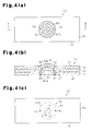
- Fig. 4 shows a case in which the solder 60 is not filled in the through holes 43 and 44 when filling the solder 60 between the first bent portion 32 and the second bent portion 42.
- the solder 60 cannot be visually checked through the through holes 43 and 44. This indicates that the soldering is defective and that the solder melted in the solder reflow process has not spread sufficiently. That is, the connection cannot be ensured.
- Factors that cause such a defect include, for example, low reflow temperature, short reflow time, and oxidation of the copper plate surface obstructing the spreading of solder.
- the through holes (43 and 44) for confirming soldering are prepared in this manner. This allows for the solder wettability to be checked during a shipment inspection.
- the through holes 43 and 44 are formed in the lower second copper plate 40.
- the filling of the solder 60 may be visually checked from the through holes 43 and 44 of the lower second copper plate 40. That is, the filling of the solder 60 may be confirmed.
- the present embodiment has the advantages described below.
- the present embodiment allows the substrate surface to be flat and facilitates the mounting of electronic components on the substrate surface. Further, the plating time does not have to be extended, and increases in the substrate cost may be avoided.
- the solder 60 which serves as a conductive material, is filled in the inner sides of the bent portions 32 and 42. This reduces the size of the space filled by the solder 60 and allows for a decrease in the amount of the filled solder 60.
- the "inner sides of the bent portions 32 and 42" correspond to the space between the first copper plate 30 and the second copper plate 40 that form a conductive line. In the first embodiment, the "inner sides of the bent portions 32 and 42" corresponds to the space between the first bent portion 32 and the second bent portion 42.
- the first copper plate 30, which serves as the first metal plate extends from the first joined portion 31, which is joined with the insulative substrate 20 that serves as the base, and includes the first bent portion 32, which is bent toward the rear side of the insulative substrate 20.
- the second copper plate 40 which serves as a second metal plate, extends from the second joined portion 41, which is joined with the insulative substrate 20, and includes the second bent portion 42, which is bent toward the front side of the insulative substrate 20 and which covers the inner wall surface of the base through hole 21 with the first bent portion 32.
- the solder 60 which serves as the conductive material, is filled between the first bent portion 32 and the second bent portion 42.
- the location filled by the solder 60 serving as the conductive material (where the solder 60 is applied) is between the first bent portion 32, which is bent toward the rear side of the insulative substrate 20, and the second bent portion 42, which is bent toward the front side of the insulative substrate 20, and is bent toward the insulative substrate 20.
- the solder 60 after melting, easily flows toward the lower side.
- the through holes 43 and 44 are formed in the second copper plate 40 at locations facing the interior of the base through hole 21. This allows for the conductive line 50 to be inspected through the through holes 43 and 44. That is, the through holes 43 and 44 allows for the filling of the solder 60 between the first bent portion 32 and the second bent portion 42 to be visually checked. Thus, the filling of the solder 60, which serves as the conductive material, in the portion forming a current line through which a large current flows may be checked.
- Fig. 1 illustrates a wiring board on which a conductive line electrically connects the first copper plate 30 and the second copper plate 40 in the base through hole 21.
- a conductive line 55 is formed to electrically connect the first copper plate 30 and the second copper plate 40 beside the insulative substrate 20.
- the conductive line 55 includes the first copper plate 30, the second copper plate 40, and solder 65 that serves as a conductive material and electrically connects the first copper plate 30 and the second copper plate 40.
- the first copper plate 30 extends from the first joined portion 31, which is joined with the insulative substrate 20, and includes a first bent portion 35, which is bent toward the rear side (lower side) of the insulative substrate 20.
- the first bent portion 35 extends straight and diagonally downward from a side surface 22 of the insulative substrate 20.
- the second copper plate 40 extends from the second joined portion 41, which is joined with the insulative substrate 20, and includes a second bent portion 45, which is bent toward the front side (upper side) of the insulative substrate 20.
- the first bent portion 35 extends straight and diagonally downward from a side surface 22 of the insulative substrate 20 and is arranged to cover the side surface 22 of the insulative substrate 20 with the first bent portion 32.
- the second bent portion 45 includes a diagonal section 45a and a horizontal section 45b.
- the diagonal section 45a of the second bent portion 42 extends straight and diagonally upward.
- the horizontal section 45b of the second bent portion 45 extends in the horizontal direction from the upper end of the diagonal section 45a.
- the upper surface of the horizontal section 45b and the upper surface of the wiring board 10 are located at the same height (flush).
- the second copper plate 40 includes a through hole 47 facing a location beside the insulative substrate 20.
- the through hole 47 is formed at a location substantially adjacent to the side surface 22 of the insulative substrate 20.
- the through hole 47 is formed in the center of the second copper plate 40 in the widthwise direction.
- the through hole 47 is circular.
- the solder 65 is filled between the first bent portion 35 and the second bent portion 45 including the interior of the through hole 47.
- the insulative substrate 20, the first copper plate 30, and the second copper plate 40 are first prepared.
- the first bent portion 35 is formed in the first copper plate 30.
- the second bent portion 45 is formed in the second copper plate 40.
- the first copper plate 30 is adhered to the upper surface of the insulative substrate 20, and the second copper plate 40 is adhered to the lower surface of the insulative substrate 20.
- the first bent portion 32 of the first copper plate 30 is positioned at where the side surface 22 of the insulative substrate 20 is located.
- the second bent portion 45 of the second copper plate 40 is arranged at where the side surface 22 of the insulative substrate 20 is located so as to cover the side surface 22 of the insulative substrate 20 with the first bent portion 35.
- a gap is formed between the first bent portion 35 and the second bent portion 45, and the gap serves as the space filled by the solder 65.
- solder paste 66 is applied to a gap between the first bent portion 35 of the first copper plate 30 and the second bent portion 45 of the second copper plate 40 beside the insulative substrate 20 and its surrounding.
- the wiring board 10 has a flat upper surface that forms a copper plate surface free of projections thereby allowing for the printing of solder paste to the desired region.
- a metal mask is arranged on a portion (distal side) of the upper surface of the horizontal section 45b in the second bent portion 45.
- solder 65 fills the space between the first bent portion 35 and the second bent portion 45 as shown in Fig. 5 .
- the solder 65 also fills the through hole 47.
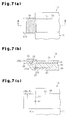
- Fig. 8 shows a case in which the solder 65 is not filled in the through hole 47 when filling the solder 65 between the first bent portion 35 and the second bent portion 45. In this case, the solder 65 cannot be visually checked through the through hole 47. This indicates that the soldering is defective.
- the present embodiment has the advantages described below.
- a bent portion may be included in only one of the first copper plate 30 and the second copper plate 40. More specifically, for example, the first copper plate 30 of Fig. 5 may horizontally extend toward the outer side from the side surface 22 of the insulative substrate 20.
- a third embodiment will now be described centering on differences from the first embodiment.
- the first copper plate 30, which serves as the first metal plate is adhered to the upper surface of the insulative substrate 20 and the second copper plate 40, which serves as the second metal plate, is adhered to the lower surface of the insulative substrate 20.
- the first copper plate 30, which is adhered to the upper surface of the insulative substrate 20, is patterned into a desired shaped to form a current line.
- the second copper plate 40, which is adhered to the lower surface of the insulative substrate 20 is patterned into a desired shaped to form a current line.
- the conductive pattern formed by the first copper plate 30 and the conductive pattern formed by the second copper plate 40 are electrically connected.
- the wiring board 10 includes the conductive line 50 that electrically connects the first copper plate 30, which is joined with the front surface (upper surface) of the insulative substrate 20, and the second copper plate 40, which is joined with the rear surface (lower surface) of the insulative substrate 20 in the base through hole 21 that extends through the insulative substrate 20.
- the base through hole 21 is circular.
- the conductive line 50 includes the first copper plate 30, the second copper plate 40, and the solder 110 that electrically connects the first copper plate 30 and the second copper plate 40.
- the first copper plate 30 includes a bent portion 37.
- the bent portion 37 extends from the first joined portion 31, which is joined with the insulative substrate 20, and bent toward the rear side (lower side) of the insulative substrate 20.
- the bent portion 37 extends straight and diagonally downward from the opening of the base through hole 21 and is arranged to cover the inner wall surface of the base through hole 21.
- a through hole 38 is formed in the first bent portion 32 at a location corresponding to the central portion of the base through hole 21.
- the through hole 38 is circular.
- the second copper plate 40 extends horizontally without being bent.
- a circular through hole 49 is formed in the second copper plate 40.
- the through hole 49 is located at the central portion of the base through hole 21.
- the interior of the base through hole 21 including the interior of the through hole 49 is filled with solder 110.
- the through hole 49 allows for gas to be released during a solder reflow process and allows for the filling of the solder 110 to be visually checked. Thus, the filling of the solder 110 may be ensured.
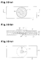
- a solder paste 111 is applied to the first copper plate 30 at the region where the through hole 38 is formed and its surrounding. Then, heating is performed in a solder reflow furnace so that fluid solder flows into the region below the application region of the solder paste 111 thereby filling the space between the first bent portion 32 and the second bent portion 42 in the base through hole 21 as shown in Fig. 9 .
- the solder 110 is also filled into the through hole 49. In this case, if there were no through hole 49, when solder melts during the solder reflow process, this would heat and increase the volume of the gas (air) trapped in the void between the solder paste 111 and the second copper plate 40.
- the solder paste 111 may be scattered.
- the present embodiment forms the through hole 49 in the second copper plate 40.
- gas may be released through the through hole 49.
- solder 110 filled in the through hole 49 from the rear surface (lower surface) of the wiring board 10
- the present embodiment has the advantages described below.
- gas may be released from the base through hole 21 through the through holes 44 and 43.
- a metal plate 270 (washer) serving as a plate material is arranged in a solder supply space.
- the metal plate 270 (washer) allows for the solder supply space to be reduced in size. This allows for a decrease in the amount of the supplied solder and allows for solder to be smoothly applied during solder application using a mask.
- the metal plate 270 (washer) and the arrangement of through holes 271, 233, and 243 in copper plates 230 and 240 allows for the release of gas and the checking of the filled solder through the through hole 243.
- a wiring board 210 is formed by a thick copper substrate. That is, the first copper plate 230, which serves as a first metal plate, is adhered to an upper surface of an insulative substrate 220, which serves as a base. Further, the second copper plate 240, which serves as a second metal plate, is adhered to a lower surface of the insulative substrate 220. The first copper plate 230 is patterned into a desired shaped to form a current line. Further, the second copper plate 240 is patterned into a desired shaped to form a current line.
- a glass epoxy resin substrate may be used as the insulative substrate 220.
- the insulative substrate 220 has a thickness of, for example, 400 ⁇ m
- the first copper plate 230 has a thickness of, for example, 500 ⁇ m
- the second copper plate 240 has a thickness of, for example, 500 ⁇ m.
- the configuration described below electrically connects a conductive pattern formed by the first copper plate 230 and a conductive pattern formed by the second copper plate 240.
- the wiring board 210 which is formed by a thick copper substrate, includes a first copper plate 230, which is joined with the front surface (upper surface) of the insulative substrate 220, and the second copper plate 240, which is joined with the rear surface (lower surface) of the insulative substrate 220 in a base through hole 221 extending through the insulative substrate 220.
- the base through hole 221 is circular.
- the conductive line 250 includes the first copper plate 230, the second copper plate 240, and solder 260 serving as a conductive material that electrically connects the first copper plate 230 and the second copper plate 240.
- the first copper plate 230 includes a first extension 232.
- the first extension 232 extends horizontally into one opening of the base through hole 221 from a first joined portion 231 joined with the insulative substrate 220. Further, the first through hole 233 is formed in the first extension 232 at a portion corresponding to the central portion of the base though hole 221.
- the first through hole 233 which is located in one opening of the base through hole 221, is circular and smaller than the base through hole 221.
- the second copper plate 240 includes a second extension 242.
- the second extension 242 extends horizontally into the other opening of the base through hole 221 from a second joined portion 241 joined with the insulative substrate 220.
- the second through hole 243 is formed in the second extension 242 at a portion corresponding to the central portion of the base though hole 221.
- the second through hole 243 which is located in the other opening of the base through hole 221, is circular, smaller than the base through hole 221, and smaller than the first through hole 233.
- the second through hole 243 is arranged in the second copper plate 240 at a portion facing the interior of the base through hole 221.
- a metal plate 27 (washer) is arranged in the base through hole 221 of the insulative substrate 220.
- the metal plate 270 is disk-shaped and engaged with the base through hole 221.
- the third through hole 271 is formed in the central portion of the metal plate 270.
- the third through hole 271 is circular.
- the third through hole 271 is in communication with the first through hole 233 and the second through hole 243. Further, the third through hole 271 is smaller than the first through hole 233 and larger than the second through hole 243.
- the interiors of the first through hole 233 and the third through hole 271 including the interior of the second through hole 243 are filled with the solder 260, which serves as the conductive material.
- the second through hole 243 allows for the filling of the solder 260 to be visually checked. That is, the filling of the solder 260 may be ensured.
- the first copper plate 230 is joined with the front surface of the insulative substrate 220, and the second copper plate 240 is joined with the rear surface of the insulative substrate 220. Further, the metal plate 270 is arranged in the base through hole 221, and the interiors of the through holes 233 and 271 including the interior of the through hole 243 are filled with the solder 260. The first copper plate 230 and the second copper plate 240 are electrically connected to each other by the solder 260.
- a large current (e.g., 120 amperes) may flow between layers.
- the through hole 243 is formed in the second copper plate 240.
- the base through hole 221 is formed in the insulative substrate 220, which serves as a core material, and adhesives 222 and 223 are applied to the two surfaces of the insulative substrate 220.
- the second copper plate 240 including the through hole 243 which is located at an opening of the base through hole 221 and is smaller than the base through hole 221, is arranged on the rear surface of the insulative substrate 220.
- the metal plate 270 which includes the through hole 271 that is in communication with the through hole 243 of the second copper plate 240 and larger than the through hole 243, is arranged in the base through hole 221.
- the metal plate 270 (washer) is just fitted. That is, the metal plate 270 (washer) is positioned at the opening of the core material (insulative substrate 220).
- the first copper plate 230 which includes the through hole 233 that is in communication with the through hole 271 of the metal plate 270, is arranged on the front surface of the insulative substrate 220.
- the lamination of the insulative substrate 220 and the copper plates 230 and 240 are heated, pressed, and completely joined by upper and lower plates 280 and 290. That is, a lamination pressing machine applies heat and pressure to join the adhesives 222 and 223.
- the interiors of the through hole 233 in the first copper plate 230 and the through hole 271 in the metal plate 270 including the interior of the through hole 243 in the second copper plate 240 are filled with the solder 260 serving as the conductive material.
- a solder paste is applied to the surface of the first copper plate 230 at the region where the through hole 233 is formed and its surrounding. Then, heating is performed in a solder reflow furnace so that fluid solder flows into the region below the application region of the solder paste thereby filling the interiors of the through hole 233 in the first copper plate 230 and the through hole 271 in the metal plate 270 including the interior of the through hole 243 in the second copper plate 240.
- the through hole 243 is formed in the second copper plate 240.
- gas air
- gas may be released through the through hole 243.
- the release of gas stabilizes the solder wettability.
- the present embodiment shown in Fig. 11 uses the metal plate 270 (washer) to raise the height. This allows for the solder amount to be decreased.
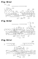
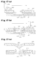
- Fig. 16 that uses the metal plate 270 (washer) will now be compared with a comparative example of Fig. 17 that does not use the metal plate 270 (washer).
- a mask 265 is arranged, and a solder paste 262 is applied to the desired region by a squeegee 266.
- the force of flux adheres the solder paste 262 to substrate side surfaces S1, S2, S3, and S4.
- the solder paste 262 is cleanly separated from the mask 265.
- Fig. 16(b) the force of flux adheres the solder paste 262 to substrate side surfaces S1, S2, S3, and S4.
- the adhering surfaces of the solder paste 262 forms S1 and S2. This decreases the adhering surfaces and lowers the adhesive force of the solder paste 262.
- the solder paste 262 may adhere to the mask 265 such that the solder paste does not remain on the substrate.
- solder paste adheres to the metal plate 27 (washer).
- the adhesion of the solder paste to the mask is obviated.
- the through hole 243 is arranged at a portion corresponding to the central portion of the base through hole 221.
- the through hole 243 may be used to release air (gas) or be used as a window used to check the filled amount of solder.
- the first extension 232 may be omitted from the first copper plate 230.
- the present embodiment obtains the advantages described below.
- the metal plate 270 (washer), which includes the through hole 271, may be adhered onto the second copper plate 240.
- the second copper plate 240 is arranged on a stage 295, and an adhesive 223 is applied to the upper surface of the second copper plate 240.
- a die 296 is arranged on the second copper plate 240, and the die 296 includes a die hole 296a.
- a metal plate 297 prior to processing is arranged on the die 296, and a stripper 298 is arranged on the metal plate 297.
- the stripper 298 includes a stripper hole 298a.
- the stripper hole 298a receives a punch 299.
- the punch 299 is lowered into the stripper hole 298a to punch out the metal plate 197 as shown in Fig. 18(b) and form the metal plate 270 (washer), which includes the through hole 271. Further, the punch 299 is lowered into the die hole 296a to press the punched out washer (metal plate 270 including through hole 271) against the adhesive 223.
- the insulative substrate 220 which includes the base through hole 221, is adhered onto the second copper plate 240.
- the washer (metal plate 270 including through hole 271) is adhered to the upper surface of the second copper plate 240. Burrs are formed when the metal plate is punched out. However, the burrs are caught in the adhesive 223. This further increases the adhesive strength.
- the adhesive 223 be conductive. Further, in Fig. 18(a) , the through hole 271 does not have to be formed beforehand in the metal plate 297.
- the wiring boards 10 and 210 do not have to be formed by thick copper substrates.
- a metal plate such as an aluminum plate may be used instead of a copper plate.
- solder As the conductive material, a different metal having a low melting point may be used.
- the number of through holes formed in the second metal plate There is no limit to the number of through holes formed in the second metal plate. For example, one to four holes may be formed. When there is a plurality of through holes, the through holes may be arranged in equal angular intervals.
- a metal plate that includes a bent portion may be extended from a joined portion joined with the base, and a metal plate that does not include a bent portion does not have to be extended from a joined portion joined with the base.
Landscapes
- Engineering & Computer Science (AREA)
- Microelectronics & Electronic Packaging (AREA)
- Manufacturing & Machinery (AREA)
- Printing Elements For Providing Electric Connections Between Printed Circuits (AREA)
Abstract
Description
- The present invention relates to a wiring board and a method for manufacturing a wiring board.
- Generally, interlayer connection is achieved in a substrate by performing copper plating. For example, as shown in
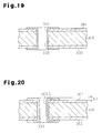
Fig. 19 , in aninsulative substrate 300, a surface layer 301 (e.g., copper foil) and a surface layer 302 (e.g., copper foil) are connected by acopper plating layer 304 formed on an inner wall surface of athrough hole 303. When the interlayer connection was performed with such typical copper plating, a large current (e.g., 120 amperes) cannot flow to thecopper plating layer 304. -
Patent document 1 discloses technology that allows for the flow of a large current. More specifically, in a printed wiring board, current through holes, which extend from a front side to a rear side of a substrate, are arranged in a concentrated manner. This allows for the flow of a large current of 50 to 180 amperes without using a bus bar. -
- Patent Document 1: Japanese Laid-Open Patent Publication No.
2010-267649 - In the structure of
Fig. 19 , a large current (e.g., 120 amperes) cannot flow through thecopper plating layer 304. Thus, referring toFig. 20 , acopper plating layer 305 having an increased thickness may be formed by extending the plating time. However, this would raise the surface of the substrate by ΔH. In a subsequent process, this would cause difficulties when mounting electronic components and when applying solder. - It is an object of the present invention to provide a wiring board and a method for manufacturing a wiring board that allow for a large current to flow through a conductive line connecting a metal plate on a front surface and a metal plate on a rear surface, while allowing for a decrease in the amount of conductive material forming the conductive line.
- To achieve the above object, a first aspect of the present invention is a wiring board provided with a base including a front surface, a rear surface, and a side surface. A first metal plate is joined with the front surface. A second metal plate is joined with the rear surface. A conductive line is configured to electrically connect the first metal plate and the second metal plate. The conductive line is arranged in an inner space defined by an inner wall surface of a base through hole formed in the base or an outer space located at an outer side of the side surface of the base. The conductive line includes the first metal plate, the second metal plate, and a conductive material electrically connecting the first metal plate and the second metal plate. At least one of the first metal plate and the second metal plate includes a joined portion, which is joined with the base, and a bent portion, which is bent and extended from the joined portion to cover the inner wall surface or the side surface. The conductive material fills an inner side of the bent portion.
- In the above structure, at least one of the first metal plate and the second metal plate includes a joined portion, which is joined with the base, and a bent portion, which is bent and extended from the joined portion to cover the inner wall surface or the side surface. The conductive material fills an inner side of the bent portion.
- The conductive line includes the first metal plate, which is joined with the front surface, the second metal plate, which is joined with the rear surface, and the conductive line, which electrically connects the first metal plate and the second metal plate. The conductive line electrically connects the first metal plate and the second metal plate in an inner space of a base through hole extending through the base or an outer space located at an outer side of the side surface of the base. This allows for a large current to flow through the conductive line connecting the first metal plate and the second metal plate. Further, the conductive material is filled in the space having a reduced size. This decreases the amount of the filled constructive material.
- Preferably, the first metal plate includes a first joined portion, which serves as the joined portion, and a first bent portion, which serves as the bent portion. The first bent portion is bent toward the rear surface. The second metal plate includes a second joined portion, which serves as the joined portion, and a second bent portion, which serves as the bent portion. The second bent portion is bent toward the front surface to cover the inner wall surface or the side surface together with the first bent portion. The conductive material is filled between the first bent portion and the second bent portion.
- The above structure allows for a large current to flow through the conductive line connecting the first metal plate and the second metal plate. The portion where the conductive material is filled is between the first bent portion, which is bent toward the rear surface of the base, and the second bent portion, which is bent toward the front surface of the substrate. The first bent portion and the second bent portion are bent toward the base. Thus, after the conductive material melts, the conductive material easily flows to the lower side.
- Preferably, the second metal board includes a through hole in a portion facing toward the inner space or the outer space.
- In the above structure, the through hole allows for either one of the release of gas from the base through hole or the inspection of the conductive line to be performed.
- Preferably, the conductive line is arranged in the inner space. The first bent portion is bent toward the inner space from an open end of the base through hole that opens in the front surface. Further, the first bent portion includes a through hole in a portion corresponding to a central portion of the base through hole. The second bent portion is bent toward the inner space from an open end of the base through hole that opens in the rear surface. Further, the second bent portion is inserted into the through hole of the first bent portion.
- The above structure ensures electrical connection with the conductive line formed in the interior space of the base through hole.
- Preferably, the through hole formed in the second metal plate is one of a plurality arranged on a circumference extending about a center axis of the base through hole, which has a circular cross-section.
- In the above structure, the plurality of through holes arranged on a circumference extending about the center axis of the base through hole, which has a circular cross-section, ensures that the conductive line may be inspected further accurately.
- Preferably, the through holes formed in the second metal plate are arranged at equal angular intervals.
- In the above structure, the through holes are arranged at equal angular intervals. This ensures that the inspection of the conductive line is performed with further accuracy.
- A second aspect of the present invention is a wiring board provided with a base including a front surface, a rear surface, and a base through hole, a first metal plate joined with the front surface, a second metal plate joined with the rear surface, and a conductive line arranged in an inner space of the base through hole to electrically connect the first metal plate and the second metal plate. The conductive line includes the first metal plate, the second metal plate, and a conductive material that electrically connects the first metal plate and the second metal plate. The second metal plate includes a joined portion, which is joined with the base, and an extended portion, which extends from the joined portion to an opening of the base through hole. A plate material, which includes a through hole that is in communication with the base through hole, is arranged in the inner space. The conductive material fills the through hole of the base material.
- The conductive line includes the first metal plate joined with the front surface, the second metal plate joined with the rear surface, and the conductive material that electrically connects the first metal plate and the second metal plate. The conductive line electrically connects the first metal plate and the second metal plate in an inner space of the base through hole that extends through the base. This allows for a large current to flow through the conductive line connecting the first metal plate and the second metal plate. Further, the plate material arranged in the space filled with the conductive material reduces the size of the space filled with the conductive material. This allows for a decrease in the amount of the filled conductive material.
- Preferably, the extended portion includes a through hole that is in communication with the through hole of the plate material.
- In the above structure, the through hole in the extended portion of the second metal plate allows for either one of the release of gas from the base through hole or the inspection of the conductive line to be performed.
- Preferably, the first metal plate includes a joined portion, which is joined with the base, and an extended portion, which extends from the joined portion to the opening of the base through hole. The extended portion includes a through hole that is smaller than the base through hole. The through hole of the plate material is in communication with the through hole of the first metal plate, and the conductive material is filled in the through hole of the first metal plate and the through hole of the plate material.
- A third aspect of the present invention is a method for manufacturing a wiring board. The wiring board is provided with a base including a front surface, a rear surface, and a side surface, a first metal plate joined with the front surface, a second metal plate joined with the rear surface, and a conductive line configured to electrically connect the first metal plate and the second metal plate. The conductive line is arranged in an inner space defined by an inner wall surface of a base through hole formed in the base, and the conductive line includes the first metal plate, the second metal plate, and a conductive material electrically connecting the first metal plate and the second metal plate. At least one of the first metal plate and the second metal plate includes a joined portion, which is joined with the base, and a bent portion, which is bent and extended from the joined portion to cover the inner wall surface. The method include the steps of joining the first metal plate with the front surface, joining the second metal plate with the rear surface to close one open end of the base through hole, applying solder paste to a front surface of the first metal plate at a portion corresponding to the other open end of the base through hole, forming a through hole in the second metal plate at a portion facing the inner space, and performing a reflow process on the solder paste to fill solder, which serves as the conductive material, into a space formed by the through hole and an inner side of the bent portion while removing gas from the through hole of the second metal plate.
- In the above configuration, in the metal plate joining step, the first metal plate is joined with the front surface of the base, and the second metal plate is joined with the rear surface to close one open end of the base through hole. In the application step, solder paste is applied to the front surface of the first metal plate at a portion corresponding to the other open end of the base through hole. In the reflow process step, a reflow process is performed on the solder paste to fill solder, which serves as the conductive material, in an inner side of the bent portion while removing gas from the through hole formed in the second metal plate at a portion facing the inner space of the base.
- This allows for the wiring board of
claim 1 to be obtained. In the reflow step performed when manufacturing the wiring board, gas is released from the base through hole. This stabilizes the solder wettability. - A fourth aspect of the present invention is a method for manufacturing a wiring board. The wiring board is provided with a base including a front surface, a rear surface, and a side surface, a first metal plate joined with the front surface, a second metal plate joined with the rear surface, and a conductive line configured to electrically connect the first metal plate and the second metal plate. The conductive line is arranged in an inner space defined by an inner wall surface of a base through hole formed in the base. The conductive line includes the first metal plate, the second metal plate, and a conductive material electrically connecting the first metal plate and the second metal plate. The method includes the steps of arranging the second metal plate that includes a through hole on the rear surface, wherein the through hole of the second metal plate is in communication with the base through hole and has a smaller opening area than the base through hole, arranging a plate material that includes a through hole in the base through hole, wherein the through hole of the plate material is in communication with the through hole of the second metal plate and has a larger opening area than the through hole of the second metal plate, arranging the first metal plate that includes a through hole on the front surface, wherein the through hole of the first metal plate is in communication with the through hole of the plate material, and filling a space formed by the through hole of the second metal plate, the through hole of the first metal plate, and the through hole of the plate material with solder, which serves as the conductive material.
- In the above configuration, in the second metal plate arranging step, the second metal plate, which includes a through hole having a smaller opening area than the base through hole and which is in communication with the base through hole, is arranged on the rear surface of the base. In the first metal plate arranging step, the first metal plate, which includes a through hole that is in communication with the through hole of the plate material, is arranged on the front surface of the base. In the filling step, an inner space of the through hole of the first metal plate and the through hole of the plate material including the through hole of the second metal plate is filled with solder, which serves as the conductive material.
- The above configuration allows for the wiring board of the second embodiment to be obtained.
- The present invention allows for a large current to flow through a conductive line connecting the front and rear sides, and allow for a decrease in the amount of the conductive material forming the conductive line.
-
-
Fig. 1(a) is a plan view of a wiring board according to a first embodiment of the present invention,Fig. 1(b) is a cross-sectional view taken along line I-I inFig. 1(a), and Fig. 1(c) is a bottom view of the wiring board. -
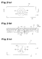
Fig. 2(a) is a plan view of the wiring board illustrating a manufacturing process for the wiring board ofFig. 1(a) ,Fig. 2(b) is a cross-sectional view taken along line II-II inFig. 2(a), and Fig. 2(c) is a bottom view of the wiring board. -
Fig. 3(a) is a plan view of the wiring board illustrating a manufacturing process for the wiring board ofFig. 1 ,Fig. 3(b) is a cross-sectional view taken along line III-III inFig. 3(a), and Fig. 3(c) is a bottom view of the wiring board. -
Fig. 4(a) is a plan view of the wiring board illustrating a manufacturing process for the wiring board ofFig. 1 ,Fig. 4(b) is a cross-sectional view taken along line IV-IV inFig. 4(a), and Fig. 4(c) is a bottom view of the wiring board. -
Fig. 5(a) is a plan view of a wiring board according to a second embodiment of the present invention,Fig. 5(b) is a cross-sectional view taken along line V-V inFig. 5(a), and Fig. 5(c) is a bottom view of the wiring board. -
Fig. 6(a) is a plan view of the wiring board illustrating a manufacturing process for the wiring board ofFig. 5(a) ,Fig. 6(b) is a cross-sectional view taken along line VI-VI inFig. 6(a), and Fig. 6(c) is a bottom view of the wiring board. -
Fig. 7(a) is a plan view of the wiring board illustrating a manufacturing process for the wiring board ofFig. 5 ,Fig. 7(b) is a cross-sectional view taken along line VII-VII inFig. 7(a), and Fig. 7(c) is a bottom view of the wiring board. -
Fig. 8(a) is a plan view of the wiring board illustrating a manufacturing process for the wiring board ofFig. 5 ,Fig. 8(b) is a cross-sectional view taken along line VIII-VIII inFig. 8(a), and Fig. 8(c) is a bottom view of the wiring board. -
Fig. 9(a) is a plan view of a wiring board according to a third embodiment of the present invention,Fig. 9(b) is a cross-sectional view taken along line IX-IX inFig. 9(a), and Fig. 9(c) is a bottom view of the wiring board. -
Fig. 10(a) is a plan view of the wiring board illustrating a manufacturing process for the wiring board ofFig. 9(a) ,Fig. 10(b) is a cross-sectional view taken along line X-X inFig. 10(a), and Fig. 10(c) is a bottom view of the wiring board. -
Fig. 11 (a) is a plan view of a wiring board according to a fourth embodiment of the present invention,Fig. 11 (b) is a cross-sectional view taken along line XI-XI inFig. 11 (a), and Fig. 11 (c) is a bottom view of the wiring board. -
Fig. 12 is an exploded cross-sectional view of the wiring board ofFig. 11 (a) . -
Figs. 13(a) to 13(c) are cross-sectional views of the wiring board ofFig. 11 (a) illustrating a manufacturing process for the wiring board. -
Figs. 14(a) and 14(b) are cross-sectional views of the wiring board ofFig. 11 (a) illustrating the manufacturing process for the wiring board. -
Fig. 15 is a cross-sectional view showing a wiring board for comparison. -
Figs. 16(a) to 16(c) are cross-sectional views illustrating a process for applying solder paste to the wiring board ofFig. 11 (a) . -
Figs. 17(a) to 17(c) are cross-sectional views illustrating a solder paste applying process for comparison. -
Figs. 18(a) to 18(c) are cross-sectional views illustrating a manufacturing process for a modified example. -
Fig. 19 is a cross-sectional view of a prior art wiring board. -
Fig. 20 is a cross-sectional view of a prior art wiring board. - A first embodiment of the present invention will now be described with reference to the drawings.
- Referring to
Fig. 1 , awiring board 10 is formed by a thick copper substrate. That is, afirst copper plate 30, which serves as a first metal plate, is adhered to an upper surface of aninsulative substrate 20, which serves as a base. Further, asecond copper plate 40, which serves as a second metal plate, is adhered to a lower surface of theinsulative substrate 20. Thefirst copper plate 30 is patterned into a desired shaped to form a current line. Further, thesecond copper plate 40 is patterned into a desired shaped to form a current line. - More specifically, for example, a glass epoxy resin substrate may be used as the
insulative substrate 20. Theinsulative substrate 20 has a thickness of, for example, 400 µm, thefirst copper plate 30 has a thickness of, for example, 500 µm, and thesecond copper plate 40 has a thickness of, for example, 500 µm. - The configuration described below electrically connects a conductive pattern formed by the
first copper plate 30 and a conductive pattern formed by thesecond copper plate 40. - In the
wiring board 10, a base throughhole 21 extends through theinsulative substrate 20. Aconductive line 50 connects thefirst copper plate 30, which is joined with the front surface (upper surface) of theinsulative substrate 20, and thesecond copper plate 40, which is joined with the rear surface (lower surface) of theinsulative substrate 20. The base throughhole 21 is circular. - The
conductive line 50 includes thefirst copper plate 30, thesecond copper plate 40, andsolder 60, which serves as a conductive material electrically connecting thefirst copper plate 30 and thesecond copper plate 40. - The
first copper plate 30 includes a firstbent portion 32. The firstbent portion 32 extends from a first joinedportion 31 and is bent toward the rear side (lower side) of theinsulative substrate 20. In detail, the firstbent portion 32 is bent into the base throughhole 21 from the open end of the base throughhole 21 in the front side (upper side) of theinsulative substrate 20. The firstbent portion 32 extends straight and diagonally downward from the opening of the base throughhole 21. A throughhole 33 is formed in the firstbent portion 32 at a location corresponding to the central portion of the base throughhole 21. The throughhole 33 is circular. - Two through
holes second copper plate 40. Thesecond copper plate 40 includes a secondbent portion 42, and the secondbent portion 42 extends from a second joinedportion 41. The secondbent portion 42 is formed at a location corresponding to the central portion of the base throughhole 21. The secondbent portion 42 includes adiagonal section 42a and ahorizontal section 42b. The secondbent portion 42 is bent toward the front side (upper side) of theinsulative substrate 20 and arranged to cover the inner wall surface of the base throughhole 21 with the firstbent portion 32. In detail, thediagonal section 42a of the secondbent portion 42 is bent to extend straight and diagonally upward into the base throughhole 21 from the opening of the base throughhole 21 in the rear side (lower side) of the insulative substrate. Further, thediagonal section 42 is inserted into the throughhole 33. Thehorizontal section 42b is located at the distal end of thediagonal section 42a. Thehorizontal section 42b is circular as viewed from above, and the upper surface of thehorizontal section 42b is horizontal. The upper surface of the horizontal section is slightly lower than the upper surface of the wiring board 10 (upper surface of the first copper plate 30). - The through holes 43 and 44 are located in the base through
hole 21 of thesecond copper plate 40. In detail, the throughholes second copper plate 40 between the periphery of the opening of the base throughhole 21 and the basal end of the secondbent portion 42. In further detail, the throughholes second copper plate 40 at locations proximal to thediagonal section 42a. The two throughholes hole 21. The through holes (43 and 44) are arranged at equal angular intervals. The through holes 43 and 44 are circular. - A space between the first
bent portion 32 and the secondbent portion 42 including the interior of the throughholes solder 60. The through holes 43 and 44 allow for the filledsolder 60 to be visible. Thus, the throughholes solder 60. - The operation of the
wiring board 10 will now be described. - In
Fig. 1 , thefirst copper plate 30 is joined with the front surface of theinsulative substrate 20, and thesecond copper plate 40 is joined with the rear surface of theinsulative substrate 20. Thesolder 60 fills the space between the firstbent portion 32 and the secondbent portion 42. Thesolder 60 electrically connects thefirst copper plate 30 and thesecond copper plate 40 to each other. - Current I flows from the
first copper plate 30 to thesecond copper plate 40. In detail, current flows from the firstbent portion 32 via thesolder 60 to the secondbent portion 42. Here, the flow of a large current (e.g., 120 amperes) is allowed. - In this manner, by devising the shapes of the
copper plates - A process for manufacturing the
wiring board 10 will now be described. - Referring to
Fig. 2 , theinsulative substrate 20, thefirst copper plate 30, and thesecond copper plate 40 are first prepared. Here, the base throughhole 21 is formed in theinsulative substrate 20. Further, the firstbent portion 32 is formed in thefirst copper plate 30. The secondbent portion 42 is formed in thesecond copper plate 40. - Then, the
first copper plate 30 is adhered to the upper surface of theinsulative substrate 20, and thesecond copper plate 40 is adhered to the lower surface of theinsulative substrate 20. Here, the firstbent portion 32 of thefirst copper plate 30 is positioned in the base throughhole 21 of theinsulative substrate 20. Further, the secondbent portion 42 of thesecond copper plate 40 is arranged in the base throughhole 21 of theinsulative substrate 20 so as to cover the inner wall surface of the base throughhole 21 with the firstbent portion 32. A gap is formed between the firstbent portion 32 and the secondbent portion 42, and the gap serves as the space filled by thesolder 60. - Subsequently, as shown in
Fig. 3 ,solder paste 61 is applied to thefirst copper plate 30 at the region where the throughhole 33 is formed (onhorizontal section 42b of the second bent portion 42) and its surrounding. The application of thesolder paste 61 is performed under a situation in which a metal mask covers a region excluding the application region of thesolder paste 61 in the base throughhole 21. Specifically, thewiring board 10 has a flat upper surface that forms a copper plate surface free of projections thereby allowing for the printing of solder paste to the desired region. Further, during a solder paste application process, in addition to the double-surface connection portion of the wiring board 10 (base through hole 21), solder paste may also be applied to a region where surface-mounted components are arranged. - Then, heating is performed in a solder reflow furnace so that fluid solder flows into between the first
bent portion 32 and the secondbent portion 42 below the application region of thesolder paste 61 thereby filling the space between the firstbent portion 32 and the secondbent portion 42. Thesolder 60 is also filled into the throughholes - By visually checking the
solder 60 filled in the throughholes bent portion 32 and the secondbent portion 42 is sufficiently filled by the reflow process. This allows for determination of whether or not soldering has been correctly performed. Specifically, thesecond copper plate 40 has a reddish black color, and thesolder 60 has a silver color. This allows for the two to be easily distinguished thereby ensuring connection. -
Fig. 4 shows a case in which thesolder 60 is not filled in the throughholes solder 60 between the firstbent portion 32 and the secondbent portion 42. In this case, thesolder 60 cannot be visually checked through the throughholes - The through holes (43 and 44) for confirming soldering are prepared in this manner. This allows for the solder wettability to be checked during a shipment inspection.
- More specifically, the through
holes second copper plate 40. When thesolder paste 61 is applied to the upperfirst copper plate 30, the filling of thesolder 60 may be visually checked from the throughholes second copper plate 40. That is, the filling of thesolder 60 may be confirmed. - The present embodiment has the advantages described below.
- (1) The
conductive line 50 is formed by thefirst copper plate 30, thesecond copper plate 40, and thesolder 60 electrically connecting thefirst copper plate 30 and thesecond copper plate 40. Theconductive line 50 electrically connects the front surface and the rear surface inside the base throughhole 21. This allows for a large current to flow through theconductive line 50 connecting the front and rear sides. - A detailed description will now be given.
- As shown in
Fig. 20 , when the plating time is extended to form a thickcopper plating layer 305 thereby allowing for the flow of a large current (e.g., 120 amperes), the surface of the substrate would be raised by ΔH, and the mounting of electronic components on the substrate surface and the application of solder in a subsequent process would be difficult. In this respect, the present embodiment allows the substrate surface to be flat and facilitates the mounting of electronic components on the substrate surface. Further, the plating time does not have to be extended, and increases in the substrate cost may be avoided. - Further, the
solder 60, which serves as a conductive material, is filled in the inner sides of thebent portions solder 60 and allows for a decrease in the amount of the filledsolder 60. The "inner sides of thebent portions first copper plate 30 and thesecond copper plate 40 that form a conductive line. In the first embodiment, the "inner sides of thebent portions bent portion 32 and the secondbent portion 42. - Further, the
first copper plate 30, which serves as the first metal plate, extends from the first joinedportion 31, which is joined with theinsulative substrate 20 that serves as the base, and includes the firstbent portion 32, which is bent toward the rear side of theinsulative substrate 20. Thesecond copper plate 40, which serves as a second metal plate, extends from the second joinedportion 41, which is joined with theinsulative substrate 20, and includes the secondbent portion 42, which is bent toward the front side of theinsulative substrate 20 and which covers the inner wall surface of the base throughhole 21 with the firstbent portion 32. Thesolder 60, which serves as the conductive material, is filled between the firstbent portion 32 and the secondbent portion 42. The location filled by thesolder 60 serving as the conductive material (where thesolder 60 is applied) is between the firstbent portion 32, which is bent toward the rear side of theinsulative substrate 20, and the secondbent portion 42, which is bent toward the front side of theinsulative substrate 20, and is bent toward theinsulative substrate 20. Thus, thesolder 60, after melting, easily flows toward the lower side. - The through holes 43 and 44 are formed in the
second copper plate 40 at locations facing the interior of the base throughhole 21. This allows for theconductive line 50 to be inspected through the throughholes holes solder 60 between the firstbent portion 32 and the secondbent portion 42 to be visually checked. Thus, the filling of thesolder 60, which serves as the conductive material, in the portion forming a current line through which a large current flows may be checked. - (2) The first
bent portion 32 includes the throughhole 33 that is bent into the base throughhole 21 from the opening of the base throughhole 21 at the front side of theinsulative substrate 20 and formed at a location corresponding to the central portion of the base throughhole 21. Further, the secondbent portion 42 is bent into the base throughhole 21 from the opening of the base throughhole 21 in the rear side of theinsulative substrate 20 and inserted into the throughhole 33 of the firstbent portion 32. Thus, theconductive line 50 formed in the base throughhole 21 may be used to ensure electric connection. - (3) The through holes (43 and 44) formed in the
second copper plate 40 are arranged along a circumference extending about the center O of the circular base throughhole 21. This further ensures accurate inspection of theconductive line 50. - (4) The through holes (43 and 44) formed in the
second copper plate 40 are arranged at equal angular intervals. This further ensures accurate inspection of theconductive line 50. - (5) Preferably, the wiring board 10 (thick copper substrate) of the present embodiment is used in an electric vehicle, a hybrid vehicle, and a train. The same applies to the wiring board (thick copper substrate) of the other embodiments.
- A second embodiment will now be described centering on differences from the first embodiment.
-
Fig. 1 illustrates a wiring board on which a conductive line electrically connects thefirst copper plate 30 and thesecond copper plate 40 in the base throughhole 21. In the present embodiment, as shown inFig. 5 , aconductive line 55 is formed to electrically connect thefirst copper plate 30 and thesecond copper plate 40 beside theinsulative substrate 20. Theconductive line 55 includes thefirst copper plate 30, thesecond copper plate 40, andsolder 65 that serves as a conductive material and electrically connects thefirst copper plate 30 and thesecond copper plate 40. - The
first copper plate 30 extends from the first joinedportion 31, which is joined with theinsulative substrate 20, and includes a firstbent portion 35, which is bent toward the rear side (lower side) of theinsulative substrate 20. The firstbent portion 35 extends straight and diagonally downward from aside surface 22 of theinsulative substrate 20. Thesecond copper plate 40 extends from the second joinedportion 41, which is joined with theinsulative substrate 20, and includes a secondbent portion 45, which is bent toward the front side (upper side) of theinsulative substrate 20. The firstbent portion 35 extends straight and diagonally downward from aside surface 22 of theinsulative substrate 20 and is arranged to cover theside surface 22 of theinsulative substrate 20 with the firstbent portion 32. - The second
bent portion 45 includes adiagonal section 45a and ahorizontal section 45b. Thediagonal section 45a of the secondbent portion 42 extends straight and diagonally upward. Further, thehorizontal section 45b of the secondbent portion 45 extends in the horizontal direction from the upper end of thediagonal section 45a. The upper surface of thehorizontal section 45b and the upper surface of the wiring board 10 (upper surface of the first copper plate 30) are located at the same height (flush). - The
second copper plate 40 includes a throughhole 47 facing a location beside theinsulative substrate 20. In detail, as shown inFig. 5(c) , the throughhole 47 is formed at a location substantially adjacent to theside surface 22 of theinsulative substrate 20. As shown inFig. 5(c) , the throughhole 47 is formed in the center of thesecond copper plate 40 in the widthwise direction. The throughhole 47 is circular. - The
solder 65 is filled between the firstbent portion 35 and the secondbent portion 45 including the interior of the throughhole 47. - A process for manufacturing the
wiring board 10 will now be described. - Referring to
Fig. 6 , theinsulative substrate 20, thefirst copper plate 30, and thesecond copper plate 40 are first prepared. The firstbent portion 35 is formed in thefirst copper plate 30. Further, the secondbent portion 45 is formed in thesecond copper plate 40. - Then, the
first copper plate 30 is adhered to the upper surface of theinsulative substrate 20, and thesecond copper plate 40 is adhered to the lower surface of theinsulative substrate 20. Here, the firstbent portion 32 of thefirst copper plate 30 is positioned at where theside surface 22 of theinsulative substrate 20 is located. Further, the secondbent portion 45 of thesecond copper plate 40 is arranged at where theside surface 22 of theinsulative substrate 20 is located so as to cover theside surface 22 of theinsulative substrate 20 with the firstbent portion 35. A gap is formed between the firstbent portion 35 and the secondbent portion 45, and the gap serves as the space filled by thesolder 65. - Subsequently, as shown in
Fig. 7 ,solder paste 66 is applied to a gap between the firstbent portion 35 of thefirst copper plate 30 and the secondbent portion 45 of thesecond copper plate 40 beside theinsulative substrate 20 and its surrounding. Specifically, thewiring board 10 has a flat upper surface that forms a copper plate surface free of projections thereby allowing for the printing of solder paste to the desired region. Further, during the application process of the solder paste, a metal mask is arranged on a portion (distal side) of the upper surface of thehorizontal section 45b in the secondbent portion 45. - Then, heating is performed in a solder reflow furnace so that the
solder 65 fills the space between the firstbent portion 35 and the secondbent portion 45 as shown inFig. 5 . Thesolder 65 also fills the throughhole 47. By visually checking thesolder 65 filled in the throughhole 47 from the rear surface (lower surface), it may be determined whether or not soldering has been correctly performed. -
Fig. 8 shows a case in which thesolder 65 is not filled in the throughhole 47 when filling thesolder 65 between the firstbent portion 35 and the secondbent portion 45. In this case, thesolder 65 cannot be visually checked through the throughhole 47. This indicates that the soldering is defective. - The present embodiment has the advantages described below.
- (5) The configuration of the wiring board includes the
first copper plate 30, which serves as the first metal plate, and thesecond copper plate 40, which serves as the second metal plate, includes thebent portions portions insulative substrate 20 serving as the base. Further, thebent portions insulative substrate 20 and arranged to cover the side surface of theinsulative substrate 20. The throughhole 47 is arranged in thesecond copper plate 40 at a portion facing a location beside theside surface 22 of theinsulative substrate 20. Further, the inner sides of thebent portions hole 47 are filled with thesolder 65 that serves as the conductive material. This allows for a large current to flow through the conductive line connecting the front and rear sides. Additionally, the space filled with thesolder 65 is small. This allows for a decrease in the amount of the filledsolder 65. Moreover, the filling of thesolder 65 serving as the conductive material at the inner sides of thebent portions hole 47. This allows for inspection of the conductive line. - A bent portion may be included in only one of the
first copper plate 30 and thesecond copper plate 40. More specifically, for example, thefirst copper plate 30 ofFig. 5 may horizontally extend toward the outer side from theside surface 22 of theinsulative substrate 20. - A third embodiment will now be described centering on differences from the first embodiment.
- As shown in
Fig. 9 , thefirst copper plate 30, which serves as the first metal plate, is adhered to the upper surface of theinsulative substrate 20 and thesecond copper plate 40, which serves as the second metal plate, is adhered to the lower surface of theinsulative substrate 20. Thefirst copper plate 30, which is adhered to the upper surface of theinsulative substrate 20, is patterned into a desired shaped to form a current line. Further, thesecond copper plate 40, which is adhered to the lower surface of theinsulative substrate 20, is patterned into a desired shaped to form a current line. - The conductive pattern formed by the
first copper plate 30 and the conductive pattern formed by thesecond copper plate 40 are electrically connected. - The
wiring board 10 includes theconductive line 50 that electrically connects thefirst copper plate 30, which is joined with the front surface (upper surface) of theinsulative substrate 20, and thesecond copper plate 40, which is joined with the rear surface (lower surface) of theinsulative substrate 20 in the base throughhole 21 that extends through theinsulative substrate 20. The base throughhole 21 is circular. - The
conductive line 50 includes thefirst copper plate 30, thesecond copper plate 40, and thesolder 110 that electrically connects thefirst copper plate 30 and thesecond copper plate 40. Thefirst copper plate 30 includes abent portion 37. Thebent portion 37 extends from the first joinedportion 31, which is joined with theinsulative substrate 20, and bent toward the rear side (lower side) of theinsulative substrate 20. Thebent portion 37 extends straight and diagonally downward from the opening of the base throughhole 21 and is arranged to cover the inner wall surface of the base throughhole 21. Further, a throughhole 38 is formed in the firstbent portion 32 at a location corresponding to the central portion of the base throughhole 21. The throughhole 38 is circular. - The
second copper plate 40 extends horizontally without being bent. A circular throughhole 49 is formed in thesecond copper plate 40. The throughhole 49 is located at the central portion of the base throughhole 21. The interior of the base throughhole 21 including the interior of the throughhole 49 is filled withsolder 110. The throughhole 49 allows for gas to be released during a solder reflow process and allows for the filling of thesolder 110 to be visually checked. Thus, the filling of thesolder 110 may be ensured. - More specifically, in the manufacturing process, as shown in
Fig. 10 , asolder paste 111 is applied to thefirst copper plate 30 at the region where the throughhole 38 is formed and its surrounding. Then, heating is performed in a solder reflow furnace so that fluid solder flows into the region below the application region of thesolder paste 111 thereby filling the space between the firstbent portion 32 and the secondbent portion 42 in the base throughhole 21 as shown inFig. 9 . Thesolder 110 is also filled into the throughhole 49. In this case, if there were no throughhole 49, when solder melts during the solder reflow process, this would heat and increase the volume of the gas (air) trapped in the void between thesolder paste 111 and thesecond copper plate 40. As a result, thesolder paste 111 may be scattered. In this regard, the present embodiment forms the throughhole 49 in thesecond copper plate 40. Thus, even when the gas trapped in the void between thesolder paste 111 and the throughhole 49 of thesecond copper plate 40 is heated, gas may be released through the throughhole 49. By releasing gas in this manner, the solder wettability is stabilized. - Further, by visually checking the
solder 110 filled in the throughhole 49 from the rear surface (lower surface) of thewiring board 10, it may be recognized that thesolder 110 has been sufficiently filled in the reflow process. This allows for determination of whether or not soldering has been correctly performed. - The present embodiment has the advantages described below.
- (6) In the configuration of the wiring board, at least one of the
first copper plate 30, which serves as the first metal plate, and thesecond copper plate 40, which serves as the second metal plate, includes thebent portion 37, which extends from the joinedportions insulative substrate 20 serving as the base. Further, thebent portion 37 is bent toward theinsulative substrate 20 and arranged to cover the inner wall surface of the base throughhole 21. Additionally, the inner side of thebent portion 37 including the interior of the throughhole 49 is filled with thesolder 110 serving as the conductive material. This allows for a large current to flow through the conductive line connecting the front and rear sides. Further, the space filled with thesolder 110 is narrow. This allows for a decrease in the amount of the filledsolder 110. Moreover, the filling of thesolder 110 serving as the conductive material at the inner side of thebent portion 37 may be visually checked from the throughhole 49. This allows for inspection of the conductive line. In broad terms, the throughhole 49 is formed in thesecond copper plate 40, which serves as the second metal plate, at a portion facing the interior of the base throughhole 21. Further, the throughhole 49 allows for at least one of the release of gas from the base throughhole 21 and the inspection of theconductive line 50 to be performed. - (7) The process for manufacturing the wiring substrate includes a metal plate joining step, an application step, and a reflow step. As shown in
Fig. 10 , in the metal plate joining step, thefirst copper plate 30, which serves as the first metal plate, is joined with the front surface of theinsulative substrate 20, which serves as the base, and thesecond copper plate 40, which serves as the second metal plate, is joined with the rear surface of theinsulative substrate 20 so as to close one opening of the base throughhole 21. In the application step,solder paste 111 is applied to the other opening of the base throughhole 21 in the front surface of thefirst copper plate 30. As shown inFig. 9 , in the reflow step, a reflow process is performed on thesolder paste 111 to fill the inner side of thebent portion 37 including the interior of the throughhole 49 with thesolder 110, which serves as the conductive material, while releasing gas from the throughhole 49 formed in a portion of thesecond copper plate 40 facing the interior of the base throughhole 21. This obtains the wiring board shown inFig. 9 . The release of gas from the base throughhole 21 in the reflow process when manufacturing the wiring board stabilizes the solder wettability. - The same applies to the through
holes Figs. 1 and3 , gas may be released from the base throughhole 21 through the throughholes - A fourth embodiment will now be described with reference to
Figs. 11 to 14 . - As shown in
Figs. 11 and12 , in the present embodiment, a metal plate 270 (washer) serving as a plate material is arranged in a solder supply space. The metal plate 270 (washer) allows for the solder supply space to be reduced in size. This allows for a decrease in the amount of the supplied solder and allows for solder to be smoothly applied during solder application using a mask. Further, the metal plate 270 (washer) and the arrangement of throughholes copper plates hole 243. - A detailed description will now be given.
- A
wiring board 210 is formed by a thick copper substrate. That is, thefirst copper plate 230, which serves as a first metal plate, is adhered to an upper surface of aninsulative substrate 220, which serves as a base. Further, thesecond copper plate 240, which serves as a second metal plate, is adhered to a lower surface of theinsulative substrate 220. Thefirst copper plate 230 is patterned into a desired shaped to form a current line. Further, thesecond copper plate 240 is patterned into a desired shaped to form a current line. - More specifically, for example, a glass epoxy resin substrate may be used as the
insulative substrate 220. Further, theinsulative substrate 220 has a thickness of, for example, 400 µm, thefirst copper plate 230 has a thickness of, for example, 500 µm, and thesecond copper plate 240 has a thickness of, for example, 500 µm. - The configuration described below electrically connects a conductive pattern formed by the
first copper plate 230 and a conductive pattern formed by thesecond copper plate 240. - The
wiring board 210, which is formed by a thick copper substrate, includes afirst copper plate 230, which is joined with the front surface (upper surface) of theinsulative substrate 220, and thesecond copper plate 240, which is joined with the rear surface (lower surface) of theinsulative substrate 220 in a base throughhole 221 extending through theinsulative substrate 220. The base throughhole 221 is circular. - The
conductive line 250 includes thefirst copper plate 230, thesecond copper plate 240, andsolder 260 serving as a conductive material that electrically connects thefirst copper plate 230 and thesecond copper plate 240. - The
first copper plate 230 includes afirst extension 232. Thefirst extension 232 extends horizontally into one opening of the base throughhole 221 from a first joinedportion 231 joined with theinsulative substrate 220. Further, the first throughhole 233 is formed in thefirst extension 232 at a portion corresponding to the central portion of the base thoughhole 221. The first throughhole 233, which is located in one opening of the base throughhole 221, is circular and smaller than the base throughhole 221. - The
second copper plate 240 includes asecond extension 242. Thesecond extension 242 extends horizontally into the other opening of the base throughhole 221 from a second joinedportion 241 joined with theinsulative substrate 220. Further, the second throughhole 243 is formed in thesecond extension 242 at a portion corresponding to the central portion of the base thoughhole 221. The second throughhole 243, which is located in the other opening of the base throughhole 221, is circular, smaller than the base throughhole 221, and smaller than the first throughhole 233. The second throughhole 243 is arranged in thesecond copper plate 240 at a portion facing the interior of the base throughhole 221. - A metal plate 27 (washer) is arranged in the base through
hole 221 of theinsulative substrate 220. Themetal plate 270 is disk-shaped and engaged with the base throughhole 221. Further, the third throughhole 271 is formed in the central portion of themetal plate 270. The third throughhole 271 is circular. The third throughhole 271 is in communication with the first throughhole 233 and the second throughhole 243. Further, the third throughhole 271 is smaller than the first throughhole 233 and larger than the second throughhole 243. - The interiors of the first through
hole 233 and the third throughhole 271 including the interior of the second throughhole 243 are filled with thesolder 260, which serves as the conductive material. The second throughhole 243 allows for the filling of thesolder 260 to be visually checked. That is, the filling of thesolder 260 may be ensured. - The operation of the
wiring board 210 will now be described. - In
Fig. 11 , thefirst copper plate 230 is joined with the front surface of theinsulative substrate 220, and thesecond copper plate 240 is joined with the rear surface of theinsulative substrate 220. Further, themetal plate 270 is arranged in the base throughhole 221, and the interiors of the throughholes hole 243 are filled with thesolder 260. Thefirst copper plate 230 and thesecond copper plate 240 are electrically connected to each other by thesolder 260. - Current flows from the
first copper plate 230 to thesecond copper plate 240. In detail, current flows from thefirst extension 232 via thesolder 260 to thesecond extension 242. Here, the flow of a large current (e.g., 120 amperes) is allowed. - In this manner, by devising the shapes of the
copper plates - Current may flow to the metal plate 270 (washer).
- A process for manufacturing the
wiring board 10 will now be described. - As shown in
Fig. 13(a) , the throughhole 243 is formed in thesecond copper plate 240. As shown inFig. 13(b) , the base throughhole 221 is formed in theinsulative substrate 220, which serves as a core material, andadhesives insulative substrate 220. Further, thesecond copper plate 240 including the throughhole 243, which is located at an opening of the base throughhole 221 and is smaller than the base throughhole 221, is arranged on the rear surface of theinsulative substrate 220. - As shown in
Fig. 13(c) , themetal plate 270, which includes the throughhole 271 that is in communication with the throughhole 243 of thesecond copper plate 240 and larger than the throughhole 243, is arranged in the base throughhole 221. When arranging the metal plate 270 (washer), the metal plate 270 (washer) is just fitted. That is, the metal plate 270 (washer) is positioned at the opening of the core material (insulative substrate 220). - As shown in
Fig. 14(a) , thefirst copper plate 230, which includes the throughhole 233 that is in communication with the throughhole 271 of themetal plate 270, is arranged on the front surface of theinsulative substrate 220. - As shown in
Fig. 14(b) , the lamination of theinsulative substrate 220 and thecopper plates lower plates adhesives - Subsequently, as shown in
Fig. 11 , the interiors of the throughhole 233 in thefirst copper plate 230 and the throughhole 271 in themetal plate 270 including the interior of the throughhole 243 in thesecond copper plate 240 are filled with thesolder 260 serving as the conductive material. - In detail, a solder paste is applied to the surface of the
first copper plate 230 at the region where the throughhole 233 is formed and its surrounding. Then, heating is performed in a solder reflow furnace so that fluid solder flows into the region below the application region of the solder paste thereby filling the interiors of the throughhole 233 in thefirst copper plate 230 and the throughhole 271 in themetal plate 270 including the interior of the throughhole 243 in thesecond copper plate 240. - In this case, the through
hole 243 is formed in thesecond copper plate 240. Thus, even when the gas (air) trapped in the void between the solder paste and thesecond copper plate 240 is heated, gas may be released through the throughhole 243. The release of gas stabilizes the solder wettability. Further, by visually checking thesolder 260 filled in the throughhole 243 from the rear surface (lower surface) of thewiring board 210, it may be recognized that thesolder 260 has been sufficiently filled in the reflow process. This allows for determination of whether or not soldering has been correctly performed. - For example, when electrically connecting layers in the case of
Fig. 15 , a large amount of solder is necessary. In this regard, the present embodiment shown inFig. 11 uses the metal plate 270 (washer) to raise the height. This allows for the solder amount to be decreased. - The present embodiment of
Fig. 16 that uses the metal plate 270 (washer) will now be compared with a comparative example ofFig. 17 that does not use the metal plate 270 (washer). When using the metal plate 270 (washer), inFigs. 16A, 16B, and 16C , amask 265 is arranged, and asolder paste 262 is applied to the desired region by asqueegee 266. Here, as shown inFig. 16(b) , the force of flux adheres thesolder paste 262 to substrate side surfaces S1, S2, S3, and S4. As shown inFig. 16(c) , when removing themask 265, thesolder paste 262 is cleanly separated from themask 265. In the case ofFig. 17 that does not use the metal plate 270 (mask), as shown inFig. 17(b) , the adhering surfaces of thesolder paste 262 forms S1 and S2. This decreases the adhering surfaces and lowers the adhesive force of thesolder paste 262. Thus, when removing themask 265, as shown inFig. 17(c) , thesolder paste 262 may adhere to themask 265 such that the solder paste does not remain on the substrate. - In this manner, in a solder paste application process, solder paste adheres to the metal plate 27 (washer). Thus, when removing the mask, the adhesion of the solder paste to the mask is obviated.
- Further, in the lower
second copper plate 240 shown inFig. 11 , the throughhole 243 is arranged at a portion corresponding to the central portion of the base throughhole 221. The throughhole 243 may be used to release air (gas) or be used as a window used to check the filled amount of solder. - The
first extension 232 may be omitted from thefirst copper plate 230. - The present embodiment obtains the advantages described below.
- (8) As the structure of the wiring board, the
second copper plate 240 includes thesecond extension 242, which extends into the opening of the base throughhole 221 from the joinedportion 241 joined with theinsulative substrate 220. Themetal plate 270 including the throughhole 271 is arranged in the base throughhole 221, and the interior of the throughhole 271 in themetal plate 270 is filled with thesolder 260, which serves as the conductive material. This allows for a large current to flow through theconductive line 250 connected the front and rear sides. Further, themetal plate 270 arranged in the space filled by thesolder 260 reduces the size of the space filled with thesolder 260. This allows for a decrease in the amount of the filledsolder 260. - (9) The
extension 242 of thesecond copper plate 240 includes the throughhole 243 that is in communication with the throughhole 271 of themetal plate 270. The throughhole 243 allows for at least one of the release of gas from the base through hole 221 (through hole 271) and the inspection of the conductive line to be performed. - (10) The
first copper plate 230 includes thefirst extension 232, which extends from the joinedportion 231 joined with theinsulative substrate 220 to the opening of the base throughhole 221 and which includes the throughhole 233 that is smaller than the base throughhole 221. Themetal plate 270, which includes the throughhole 271 that is in communication with the throughhole 233 of thefirst copper plate 230, is arranged in the base throughhole 221. The interiors of the throughhole 233 in thefirst copper plate 230 and the throughhole 271 in themetal plate 270 are filled with thesolder 260, which serves as the conductive material. Thus, themetal plate 270 is preferable for positioning. - (11) The process for manufacturing the wiring board includes a second metal plate arrangement step, a plate material arrangement step, a first metal plate arrangement step, and a solder filling step. In the second metal plate arrangement step, the
second copper plate 240, which is located in the opening of the base throughhole 221 and includes the throughhole 243 that is smaller than the base throughhole 221, is arranged on the rear surface of theinsulative substrate 220. In the plate material arrangement step, themetal plate 270, which includes the throughhole 271 that is in communication with the throughhole 243 of thesecond copper plate 240 and is larger than the throughhole 243 of thesecond copper plate 240, is arranged in the base throughhole 221. In the first metal plate arrangement step, thefirst copper plate 230, which includes the throughhole 233 that is in communication with the throughhole 271 of themetal plate 270, is arranged on the front surface of theinsulative substrate 220. In the solder filling step, the interiors of the throughhole 233 in thefirst copper plate 230 and the throughhole 271 in themetal plate 270 including the interior of the throughhole 243 in thesecond copper plate 240 are filled with thesolder 260, which serves as the conductive material. This allows for the wiring board of (10) to be obtained. - Modified examples of the present embodiment will now be described.
- As shown in
Fig. 18(c) , the metal plate 270 (washer), which includes the throughhole 271, may be adhered onto thesecond copper plate 240. In detail, as shown inFig. 18(a) , thesecond copper plate 240 is arranged on astage 295, and an adhesive 223 is applied to the upper surface of thesecond copper plate 240. Adie 296 is arranged on thesecond copper plate 240, and thedie 296 includes adie hole 296a. Ametal plate 297 prior to processing is arranged on thedie 296, and astripper 298 is arranged on themetal plate 297. Thestripper 298 includes a stripper hole 298a. The stripper hole 298a receives apunch 299. - The
punch 299 is lowered into the stripper hole 298a to punch out the metal plate 197 as shown inFig. 18(b) and form the metal plate 270 (washer), which includes the throughhole 271. Further, thepunch 299 is lowered into thedie hole 296a to press the punched out washer (metal plate 270 including through hole 271) against the adhesive 223. - Subsequently, the
punch 299 is raised, and thedie 296 is raised. As shown inFig. 18(c) , this adheres the metal plate 270 (washer) including the throughhole 271 onto thesecond copper plate 240. - Then, as shown in
Fig. 13(c) , theinsulative substrate 220, which includes the base throughhole 221, is adhered onto thesecond copper plate 240. - As illustrated in
Fig. 18 , the washer (metal plate 270 including through hole 271) is adhered to the upper surface of thesecond copper plate 240. Burrs are formed when the metal plate is punched out. However, the burrs are caught in the adhesive 223. This further increases the adhesive strength. - In this case, it is preferable that the adhesive 223 be conductive. Further, in
Fig. 18(a) , the throughhole 271 does not have to be formed beforehand in themetal plate 297. - The embodiments are not limited to the foregoing description and may take the following forms.
- The
wiring boards - Instead of using solder as the conductive material, a different metal having a low melting point may be used.
- There is no restriction to the bending angle of the first
bent portion 32, the bending angle of the second bent portion 42 (diagonal section 42a), the bending angle of the firstbent portion 35, and the bending angle of the second bent portion 45 (diagonal section 45a). - There is no limit to the number of through holes formed in the second metal plate. For example, one to four holes may be formed. When there is a plurality of through holes, the through holes may be arranged in equal angular intervals.
- In the first to third embodiments, a metal plate that includes a bent portion may be extended from a joined portion joined with the base, and a metal plate that does not include a bent portion does not have to be extended from a joined portion joined with the base.
- 10: wiring board, 20: insulative substrate, 21: base through hole, 22: side surface, 30: first copper plate, 31: first joined portion, 32: first bent portion, 33: through hole, 35: first bent portion, 37: bent portion, 40: second copper plate, 41: second joined portion, 42: second bent portion, 43: through hole, 44: through hole, 45: second bent portion, 47: through hole, 49: through hole, 50: conductive line, 55: conductive line, 60: solder, 65: solder, 110: solder, 210: wiring board, 220: insulative substrate, 221: base through hole, 230: first copper plate, 231: first joined portion, 232: first extended portion, 233: first through hole, 240: second copper plate, 241: second joined portion, 242: second extended portion, 243: second through hole, 250: conductive line, 260: solder, 270: metal plate, 271: third through hole
Claims (11)
- A wiring board comprising:a base including a front surface, a rear surface, and a side surface;a first metal plate joined with the front surface;a second metal plate joined with the rear surface; anda conductive line configured to electrically connect the first metal plate and the second metal plate, wherein the conductive line is arranged in an inner space defined by an inner wall surface of a base through hole formed in the base or an outer space located at an outer side of the side surface of the base, and the conductive line includes the first metal plate, the second metal plate, and a conductive material electrically connecting the first metal plate and the second metal plate,wherein at least one of the first metal plate and the second metal plate includes a joined portion, which is joined with the base, and a bent portion, which is bent and extended from the joined portion to cover the inner wall surface or the side surface, andthe conductive material fills an inner side of the bent portion.
- The wiring board according to claim 1, wherein
the first metal plate includes a first joined portion, which serves as the joined portion, and a first bent portion, which serves as the bent portion, and the first bent portion is bent toward the rear surface;
the second metal plate includes a second joined portion, which serves as the joined portion, and a second bent portion, which serves as the bent portion, and the second bent portion is bent toward the front surface to cover the inner wall surface or the side surface together with the first bent portion; and
the conductive material is filled between the first bent portion and the second bent portion. - The wiring board according to claim 1 or 2, wherein the second metal board includes a through hole in a portion facing toward the inner space or the outer space.
- The wiring board according to claim 2 or 3, wherein
the conductive line is arranged in the inner space;
the first bent portion is bent toward the inner space from an open end of the base through hole that opens in the front surface, and the first bent portion includes a through hole in a portion corresponding to a central portion of the base through hole; and
the second bent portion is bent toward the inner space from an open end of the base through hole that opens in the rear surface, and the second bent portion is inserted into the through hole of the first bent portion. - The wiring board according to claim 3, wherein the through hole formed in the second metal plate is one of a plurality of through holes arranged on a circumference extending about a center axis of the base through hole, which has a circular cross-section.
- The wiring board according to claim 5, wherein the through holes formed in the second metal plate are arranged at equal angular intervals.
- A wiring board comprising:a base including a front surface, a rear surface, and a base through hole;a first metal plate joined with the front surface;a second metal plate joined with the rear surface; anda conductive line arranged in an inner space of the base through hole to electrically connect the first metal plate and the second metal plate, wherein the conductive line includes the first metal plate, the second metal plate, and a conductive material that electrically connects the first metal plate and the second metal plate,wherein the second metal plate includes a joined portion, which is joined with the base, and an extended portion, which extends from the joined portion to an opening of the base through hole,a plate material, which includes a through hole that is in communication with the base through hole, is arranged in the inner space, andthe conductive material fills the through hole of the base material.
- The wiring board according to claim 7, wherein the extended portion includes a through hole that is in communication with the through hole of the plate material.
- The wiring board according to claim 7 or 8, wherein
the first metal plate includes a joined portion, which is joined with the base, and an extended portion, which extends from the joined portion to the opening of the base through hole, wherein the extended portion includes a through hole that is smaller than the base through hole; and
the through hole of the plate material is in communication with the through hole of the first metal plate, and the conductive material is filled in the through hole of the first metal plate and the through hole of the plate material. - A method for manufacturing a wiring board including
a base including a front surface, a rear surface, and a side surface;
a first metal plate joined with the front surface;
a second metal plate joined with the rear surface; and
a conductive line configured to electrically connect the first metal plate and the second metal plate, wherein the conductive line is arranged in an inner space defined by an inner wall surface of a base through hole formed in the base, and the conductive line includes the first metal plate, the second metal plate, and a conductive material electrically connecting the first metal plate and the second metal plate,
wherein at least one of the first metal plate and the second metal plate includes a joined portion, which is joined with the base, and a bent portion, which is bent and extended from the joined portion to cover the inner wall surface,
the method comprising the steps of:joining the first metal plate with the front surface;joining the second metal plate with the rear surface to close one open end of the base through hole;applying solder paste to a front surface of the first metal plate at a portion corresponding to the other open end of the base through hole;forming a through hole in the second metal plate at a portion facing the inner space; andperforming a reflow process on the solder paste to fill solder, which serves as the conductive material, into a space formed by the through hole and an inner side of the bent portion while removing gas from the through hole of the second metal plate. - A method for manufacturing a wiring board including
a base including a front surface, a rear surface, and a side surface;
a first metal plate joined with the front surface;
a second metal plate joined with the rear surface; and
a conductive line configured to electrically connect the first metal plate and the second metal plate, wherein the conductive line is arranged in an inner space defined by an inner wall surface of a base through hole formed in the base, and the conductive line includes the first metal plate, the second metal plate, and a conductive material electrically connecting the first metal plate and the second metal plate,
the method comprising the steps of:arranging the second metal plate that includes a through hole on the rear surface, wherein the through hole of the second metal plate is in communication with the base through hole and has a smaller opening area than the base through hole;arranging a plate material that includes a through hole in the base through hole, wherein the through hole of the plate material is in communication with the through hole of the second metal plate and has a larger opening area than the through hole of the second metal plate;arranging the first metal plate that includes a through hole on the front surface, wherein the through hole of the first metal plate is in communication with the through hole of the plate material; andfilling a space formed by the through hole of the second metal plate, the through hole of the first metal plate, and the through hole of the plate material with solder, which serves as the conductive material.
Applications Claiming Priority (2)
| Application Number | Priority Date | Filing Date | Title |
|---|---|---|---|
| JP2011118332 | 2011-05-26 | ||
| PCT/JP2012/063186 WO2012161218A1 (en) | 2011-05-26 | 2012-05-23 | Wiring board and method for manufacturing wiring board |
Publications (3)
| Publication Number | Publication Date |
|---|---|
| EP2717658A1 true EP2717658A1 (en) | 2014-04-09 |
| EP2717658A4 EP2717658A4 (en) | 2015-08-12 |
| EP2717658B1 EP2717658B1 (en) | 2017-10-18 |
Family
ID=47217294
Family Applications (1)
| Application Number | Title | Priority Date | Filing Date |
|---|---|---|---|
| EP12789574.6A Not-in-force EP2717658B1 (en) | 2011-05-26 | 2012-05-23 | Wiring board and method for manufacturing wiring board |
Country Status (7)
| Country | Link |
|---|---|
| US (1) | US9332638B2 (en) |
| EP (1) | EP2717658B1 (en) |
| JP (1) | JP5742936B2 (en) |
| KR (1) | KR20130140889A (en) |
| CN (1) | CN103563495B (en) |
| TW (1) | TWI451817B (en) |
| WO (1) | WO2012161218A1 (en) |
Cited By (1)
| Publication number | Priority date | Publication date | Assignee | Title |
|---|---|---|---|---|
| EP3822997A4 (en) * | 2018-06-05 | 2022-04-06 | Nippon Chemi-Con Corporation | BUS BAR LAMINATE, ELECTRONIC COMPONENT MOUNTING MODULE WITH THE SAME, AND METHOD OF MAKING BUS BAR LAMINATE |
Families Citing this family (4)
| Publication number | Priority date | Publication date | Assignee | Title |
|---|---|---|---|---|
| JP5807670B2 (en) * | 2013-12-19 | 2015-11-10 | 株式会社豊田自動織機 | Wiring board |
| JP5807671B2 (en) * | 2013-12-19 | 2015-11-10 | 株式会社豊田自動織機 | Wiring board and method of manufacturing wiring board |
| WO2015125951A1 (en) * | 2014-02-24 | 2015-08-27 | 株式会社村田製作所 | Manufacturing method for multilayer substrate and multilayer substrate |
| JP7433796B2 (en) * | 2019-07-24 | 2024-02-20 | デクセリアルズ株式会社 | protection element |
Family Cites Families (26)
| Publication number | Priority date | Publication date | Assignee | Title |
|---|---|---|---|---|
| JPS5511174Y2 (en) * | 1972-11-29 | 1980-03-11 | ||
| US4064357A (en) * | 1975-12-02 | 1977-12-20 | Teledyne Electro-Mechanisms | Interconnected printed circuits and method of connecting them |
| JPS54156167A (en) * | 1978-05-31 | 1979-12-08 | Matsushita Electric Industrial Co Ltd | Method of producing double side printed circuit board |
| FR2439322A1 (en) * | 1978-10-19 | 1980-05-16 | Cii Honeywell Bull | METHOD AND DEVICE FOR CONNECTING TWO ELEMENTS AND TOOL FOR EXECUTING THE PROCESS |
| CA1100319A (en) | 1979-05-10 | 1981-05-05 | Eugene E. Young | Oil return system and method |
| GB2085233A (en) * | 1980-08-19 | 1982-04-21 | Renishaw Electrical Ltd | Electric circuit board assembly |
| US4769269A (en) * | 1983-12-05 | 1988-09-06 | E. I. Du Pont De Nemours And Company | Article containing conductive through-holes |
| JPH0437087A (en) * | 1990-05-31 | 1992-02-07 | Toshiba Corp | Printed-wiring board device, eyelet therefor and mounting thereof |
| CA2114792A1 (en) | 1992-06-15 | 1993-12-16 | Walter Schmidt | Process for producing subsequently conditionable contact points on circuit substrates and circuit substrates with such contact points |
| ATE135521T1 (en) * | 1992-06-15 | 1996-03-15 | Heinze Dyconex Patente | METHOD FOR PRODUCING SUBSTRATES WITH THROUGH THROUGH |
| EP0600051B1 (en) | 1992-06-15 | 1999-05-12 | Dyconex Patente Ag | Process for producing printed circuit boards using a semi-finished product with extremely dense wiring for signal conduction |
| US5433819A (en) * | 1993-05-26 | 1995-07-18 | Pressac, Inc. | Method of making circuit boards |
| JP3052855B2 (en) * | 1996-10-21 | 2000-06-19 | 日本電気株式会社 | Wiring board |
| TW512467B (en) * | 1999-10-12 | 2002-12-01 | North Kk | Wiring circuit substrate and manufacturing method therefor |
| DE10007414B4 (en) * | 2000-02-18 | 2006-07-06 | eupec Europäische Gesellschaft für Leistungshalbleiter mbH & Co. KG | Process for the through-plating of a substrate for power semiconductor modules by solder and substrate produced by the method |
| JP2002185120A (en) * | 2000-12-19 | 2002-06-28 | Toshiba Corp | Component mounting board and method of manufacturing the same |
| JP2005072095A (en) * | 2003-08-20 | 2005-03-17 | Alps Electric Co Ltd | Electronic circuit unit and manufacturing method thereof |
| JP2006093577A (en) | 2004-09-27 | 2006-04-06 | Hitachi Cable Ltd | Transfer film substrate for semiconductor device, manufacturing method thereof, and semiconductor device using the same |
| JP2006303126A (en) * | 2005-04-20 | 2006-11-02 | Oki Electric Ind Co Ltd | Method of manufacturing printed wiring board |
| US7649748B2 (en) * | 2005-06-15 | 2010-01-19 | Ibiden Co., Ltd. | Multilayer printed wiring board |
| JP2008021637A (en) * | 2006-06-12 | 2008-01-31 | Fujikura Ltd | Socket, manufacturing method thereof, and semiconductor device |
| JP5629580B2 (en) * | 2007-09-28 | 2014-11-19 | テッセラ,インコーポレイテッド | Flip chip interconnect with double posts |
| US8324723B2 (en) * | 2008-03-25 | 2012-12-04 | Bridge Semiconductor Corporation | Semiconductor chip assembly with bump/base heat spreader and dual-angle cavity in bump |
| EP2236330B1 (en) * | 2009-03-30 | 2011-09-28 | Eberspächer catem GmbH & Co. KG | Electric heater for a motor vehicle |
| JP2010267649A (en) | 2009-05-12 | 2010-11-25 | Tibc:Kk | Printed wiring board |
| TWI400025B (en) * | 2009-12-29 | 2013-06-21 | Subtron Technology Co Ltd | Circuit substrate and manufacturing method thereof |
-
2012
- 2012-05-22 TW TW101118142A patent/TWI451817B/en not_active IP Right Cessation
- 2012-05-23 EP EP12789574.6A patent/EP2717658B1/en not_active Not-in-force
- 2012-05-23 US US14/118,636 patent/US9332638B2/en not_active Expired - Fee Related
- 2012-05-23 KR KR1020137030367A patent/KR20130140889A/en not_active Ceased
- 2012-05-23 WO PCT/JP2012/063186 patent/WO2012161218A1/en not_active Ceased
- 2012-05-23 CN CN201280024409.6A patent/CN103563495B/en not_active Expired - Fee Related
- 2012-05-23 JP JP2013516414A patent/JP5742936B2/en not_active Expired - Fee Related
Cited By (1)
| Publication number | Priority date | Publication date | Assignee | Title |
|---|---|---|---|---|
| EP3822997A4 (en) * | 2018-06-05 | 2022-04-06 | Nippon Chemi-Con Corporation | BUS BAR LAMINATE, ELECTRONIC COMPONENT MOUNTING MODULE WITH THE SAME, AND METHOD OF MAKING BUS BAR LAMINATE |
Also Published As
| Publication number | Publication date |
|---|---|
| US9332638B2 (en) | 2016-05-03 |
| KR20130140889A (en) | 2013-12-24 |
| WO2012161218A1 (en) | 2012-11-29 |
| CN103563495B (en) | 2016-10-12 |
| EP2717658B1 (en) | 2017-10-18 |
| JP5742936B2 (en) | 2015-07-01 |
| US20140151106A1 (en) | 2014-06-05 |
| TW201301965A (en) | 2013-01-01 |
| TWI451817B (en) | 2014-09-01 |
| JPWO2012161218A1 (en) | 2014-07-31 |
| CN103563495A (en) | 2014-02-05 |
| EP2717658A4 (en) | 2015-08-12 |
Similar Documents
| Publication | Publication Date | Title |
|---|---|---|
| US7870663B2 (en) | Method for manufacturing multilayer wiring board | |
| CN1939104B (en) | Rigid-flexible board and method for manufacturing same | |
| US9332638B2 (en) | Wiring board and method for manufacturing wiring board | |
| WO2000072644A1 (en) | Sheet for printed wiring board, method of forming via, resin sheet having filled via, printed wiring board and method of manufacturing the same | |
| CN104206037B (en) | Method for manufacturing a circuit board comprising at least two circuit board areas and circuit board | |
| CN103687308B (en) | Blind hole crimping multilayer board and preparation method thereof | |
| CN103188882A (en) | Circuit board and manufacture method thereof | |
| CN104685590A (en) | Solid electrolytic capacitor and production method therefor | |
| US9093775B2 (en) | Connection pin for mounting in a component carrier, a method for producing an electronic assembly comprising a motherboard with stackable modules comprising a component carrier, and such an electronic assembly | |
| US20170034911A1 (en) | Resin multilayer substrate and method of manufacturing the same | |
| TW201108903A (en) | Printed wiring board and method for producing the same | |
| CN214800032U (en) | Metal-based FR4 mixed-compression substrate | |
| JP2007173342A (en) | Substrate mounting structure, mounting method thereof and alignment plate structure used therefor | |
| CN101808472A (en) | Method for producing electronic part unit | |
| CN210725561U (en) | Conductive paste grouting hole circuit board lamp strip with low cost and low resistance value | |
| CN206231042U (en) | Metal mask | |
| JP2006100703A (en) | Rigid-flexible substrate and manufacturing method thereof | |
| JP2005039136A (en) | Circuit board and method for connection thereof | |
| JP5703529B2 (en) | Printed wiring board and method for manufacturing printed wiring board | |
| US7943860B2 (en) | Material board for producing hybrid circuit board with metallic terminal plate and method for producing hybrid circuit board | |
| CN112135435B (en) | A light strip made of a bowl-hole double-sided circuit board and a manufacturing method thereof | |
| JP4277723B2 (en) | Multilayer circuit board and method for manufacturing multilayer circuit board | |
| JP2010278380A (en) | Wiring board manufacturing method and wiring board | |
| CN112702830A (en) | Anti-pulling circuit board and manufacturing method thereof | |
| JP2009105293A (en) | Conductive connecting material and module manufacturing method |
Legal Events
| Date | Code | Title | Description |
|---|---|---|---|
| PUAI | Public reference made under article 153(3) epc to a published international application that has entered the european phase |
Free format text: ORIGINAL CODE: 0009012 |
|
| 17P | Request for examination filed |
Effective date: 20131202 |
|
| AK | Designated contracting states |
Kind code of ref document: A1 Designated state(s): AL AT BE BG CH CY CZ DE DK EE ES FI FR GB GR HR HU IE IS IT LI LT LU LV MC MK MT NL NO PL PT RO RS SE SI SK SM TR |
|
| RIN1 | Information on inventor provided before grant (corrected) |
Inventor name: KOIKE, YASUHIRO Inventor name: HAYAKAWA, TAKAHIRO Inventor name: KACHI, TADAYOSHI Inventor name: WATANABE, HIROKI Inventor name: SHIMADU, HITOSHI Inventor name: MIYAKE, MASAO Inventor name: FURUTA, TETSUYA Inventor name: OZAKI, KIMINORI Inventor name: YAMAUCHI, RYOU Inventor name: ASAI, TOMOAKI Inventor name: SUZUKI, TAKAHIRO Inventor name: SATO, HARUMITSU Inventor name: ASANO, HIROAKI |
|
| DAX | Request for extension of the european patent (deleted) | ||
| RIC1 | Information provided on ipc code assigned before grant |
Ipc: H05K 3/00 20060101ALN20150319BHEP Ipc: H05K 1/11 20060101ALN20150319BHEP Ipc: H05K 1/02 20060101ALN20150319BHEP Ipc: H05K 3/40 20060101AFI20150319BHEP |
|
| RA4 | Supplementary search report drawn up and despatched (corrected) |
Effective date: 20150710 |
|
| RIC1 | Information provided on ipc code assigned before grant |
Ipc: H05K 1/02 20060101ALN20150706BHEP Ipc: H05K 3/40 20060101AFI20150706BHEP Ipc: H05K 3/00 20060101ALN20150706BHEP Ipc: H05K 1/11 20060101ALN20150706BHEP |
|
| REG | Reference to a national code |
Ref country code: DE Ref legal event code: R079 Ref document number: 602012038725 Country of ref document: DE Free format text: PREVIOUS MAIN CLASS: H05K0001110000 Ipc: H05K0003400000 |
|
| RIC1 | Information provided on ipc code assigned before grant |
Ipc: H05K 1/02 20060101ALN20170324BHEP Ipc: H05K 3/00 20060101ALN20170324BHEP Ipc: H05K 3/40 20060101AFI20170324BHEP Ipc: H05K 1/11 20060101ALN20170324BHEP |
|
| GRAP | Despatch of communication of intention to grant a patent |
Free format text: ORIGINAL CODE: EPIDOSNIGR1 |
|
| INTG | Intention to grant announced |
Effective date: 20170509 |
|
| RIN1 | Information on inventor provided before grant (corrected) |
Inventor name: SUZUKI, TAKAHIRO Inventor name: ASAI, TOMOAKI Inventor name: FURUTA, TETSUYA Inventor name: SATO, HARUMITSU Inventor name: ASANO, HIROAKI Inventor name: SHIMADU, HITOSHI Inventor name: HAYAKAWA, TAKAHIRO Inventor name: KOIKE, YASUHIRO Inventor name: OZAKI, KIMINORI Inventor name: KACHI, TADAYOSHI Inventor name: WATANABE, HIROKI Inventor name: YAMAUCHI, RYOU Inventor name: MIYAKE, MASAO |
|
| GRAS | Grant fee paid |
Free format text: ORIGINAL CODE: EPIDOSNIGR3 |
|
| GRAA | (expected) grant |
Free format text: ORIGINAL CODE: 0009210 |
|
| AK | Designated contracting states |
Kind code of ref document: B1 Designated state(s): AL AT BE BG CH CY CZ DE DK EE ES FI FR GB GR HR HU IE IS IT LI LT LU LV MC MK MT NL NO PL PT RO RS SE SI SK SM TR |
|
| REG | Reference to a national code |
Ref country code: GB Ref legal event code: FG4D |
|
| REG | Reference to a national code |
Ref country code: CH Ref legal event code: EP |
|
| REG | Reference to a national code |
Ref country code: AT Ref legal event code: REF Ref document number: 938978 Country of ref document: AT Kind code of ref document: T Effective date: 20171115 Ref country code: IE Ref legal event code: FG4D |
|
| REG | Reference to a national code |
Ref country code: DE Ref legal event code: R096 Ref document number: 602012038725 Country of ref document: DE |
|
| REG | Reference to a national code |
Ref country code: NL Ref legal event code: MP Effective date: 20171018 |
|
| REG | Reference to a national code |
Ref country code: LT Ref legal event code: MG4D |
|
| REG | Reference to a national code |
Ref country code: AT Ref legal event code: MK05 Ref document number: 938978 Country of ref document: AT Kind code of ref document: T Effective date: 20171018 |
|
| PG25 | Lapsed in a contracting state [announced via postgrant information from national office to epo] |
Ref country code: NL Free format text: LAPSE BECAUSE OF FAILURE TO SUBMIT A TRANSLATION OF THE DESCRIPTION OR TO PAY THE FEE WITHIN THE PRESCRIBED TIME-LIMIT Effective date: 20171018 |
|
| PG25 | Lapsed in a contracting state [announced via postgrant information from national office to epo] |
Ref country code: FI Free format text: LAPSE BECAUSE OF FAILURE TO SUBMIT A TRANSLATION OF THE DESCRIPTION OR TO PAY THE FEE WITHIN THE PRESCRIBED TIME-LIMIT Effective date: 20171018 Ref country code: LT Free format text: LAPSE BECAUSE OF FAILURE TO SUBMIT A TRANSLATION OF THE DESCRIPTION OR TO PAY THE FEE WITHIN THE PRESCRIBED TIME-LIMIT Effective date: 20171018 Ref country code: NO Free format text: LAPSE BECAUSE OF FAILURE TO SUBMIT A TRANSLATION OF THE DESCRIPTION OR TO PAY THE FEE WITHIN THE PRESCRIBED TIME-LIMIT Effective date: 20180118 Ref country code: SE Free format text: LAPSE BECAUSE OF FAILURE TO SUBMIT A TRANSLATION OF THE DESCRIPTION OR TO PAY THE FEE WITHIN THE PRESCRIBED TIME-LIMIT Effective date: 20171018 Ref country code: ES Free format text: LAPSE BECAUSE OF FAILURE TO SUBMIT A TRANSLATION OF THE DESCRIPTION OR TO PAY THE FEE WITHIN THE PRESCRIBED TIME-LIMIT Effective date: 20171018 |
|
| PG25 | Lapsed in a contracting state [announced via postgrant information from national office to epo] |
Ref country code: LV Free format text: LAPSE BECAUSE OF FAILURE TO SUBMIT A TRANSLATION OF THE DESCRIPTION OR TO PAY THE FEE WITHIN THE PRESCRIBED TIME-LIMIT Effective date: 20171018 Ref country code: GR Free format text: LAPSE BECAUSE OF FAILURE TO SUBMIT A TRANSLATION OF THE DESCRIPTION OR TO PAY THE FEE WITHIN THE PRESCRIBED TIME-LIMIT Effective date: 20180119 Ref country code: AT Free format text: LAPSE BECAUSE OF FAILURE TO SUBMIT A TRANSLATION OF THE DESCRIPTION OR TO PAY THE FEE WITHIN THE PRESCRIBED TIME-LIMIT Effective date: 20171018 Ref country code: RS Free format text: LAPSE BECAUSE OF FAILURE TO SUBMIT A TRANSLATION OF THE DESCRIPTION OR TO PAY THE FEE WITHIN THE PRESCRIBED TIME-LIMIT Effective date: 20171018 Ref country code: BG Free format text: LAPSE BECAUSE OF FAILURE TO SUBMIT A TRANSLATION OF THE DESCRIPTION OR TO PAY THE FEE WITHIN THE PRESCRIBED TIME-LIMIT Effective date: 20180118 Ref country code: IS Free format text: LAPSE BECAUSE OF FAILURE TO SUBMIT A TRANSLATION OF THE DESCRIPTION OR TO PAY THE FEE WITHIN THE PRESCRIBED TIME-LIMIT Effective date: 20180218 Ref country code: HR Free format text: LAPSE BECAUSE OF FAILURE TO SUBMIT A TRANSLATION OF THE DESCRIPTION OR TO PAY THE FEE WITHIN THE PRESCRIBED TIME-LIMIT Effective date: 20171018 |
|
| REG | Reference to a national code |
Ref country code: DE Ref legal event code: R097 Ref document number: 602012038725 Country of ref document: DE |
|
| PG25 | Lapsed in a contracting state [announced via postgrant information from national office to epo] |
Ref country code: EE Free format text: LAPSE BECAUSE OF FAILURE TO SUBMIT A TRANSLATION OF THE DESCRIPTION OR TO PAY THE FEE WITHIN THE PRESCRIBED TIME-LIMIT Effective date: 20171018 Ref country code: CZ Free format text: LAPSE BECAUSE OF FAILURE TO SUBMIT A TRANSLATION OF THE DESCRIPTION OR TO PAY THE FEE WITHIN THE PRESCRIBED TIME-LIMIT Effective date: 20171018 Ref country code: SK Free format text: LAPSE BECAUSE OF FAILURE TO SUBMIT A TRANSLATION OF THE DESCRIPTION OR TO PAY THE FEE WITHIN THE PRESCRIBED TIME-LIMIT Effective date: 20171018 Ref country code: DK Free format text: LAPSE BECAUSE OF FAILURE TO SUBMIT A TRANSLATION OF THE DESCRIPTION OR TO PAY THE FEE WITHIN THE PRESCRIBED TIME-LIMIT Effective date: 20171018 |
|
| PLBE | No opposition filed within time limit |
Free format text: ORIGINAL CODE: 0009261 |
|
| STAA | Information on the status of an ep patent application or granted ep patent |
Free format text: STATUS: NO OPPOSITION FILED WITHIN TIME LIMIT |
|
| PG25 | Lapsed in a contracting state [announced via postgrant information from national office to epo] |
Ref country code: PL Free format text: LAPSE BECAUSE OF FAILURE TO SUBMIT A TRANSLATION OF THE DESCRIPTION OR TO PAY THE FEE WITHIN THE PRESCRIBED TIME-LIMIT Effective date: 20171018 Ref country code: SM Free format text: LAPSE BECAUSE OF FAILURE TO SUBMIT A TRANSLATION OF THE DESCRIPTION OR TO PAY THE FEE WITHIN THE PRESCRIBED TIME-LIMIT Effective date: 20171018 Ref country code: RO Free format text: LAPSE BECAUSE OF FAILURE TO SUBMIT A TRANSLATION OF THE DESCRIPTION OR TO PAY THE FEE WITHIN THE PRESCRIBED TIME-LIMIT Effective date: 20171018 Ref country code: IT Free format text: LAPSE BECAUSE OF FAILURE TO SUBMIT A TRANSLATION OF THE DESCRIPTION OR TO PAY THE FEE WITHIN THE PRESCRIBED TIME-LIMIT Effective date: 20171018 |
|
| 26N | No opposition filed |
Effective date: 20180719 |
|
| PG25 | Lapsed in a contracting state [announced via postgrant information from national office to epo] |
Ref country code: SI Free format text: LAPSE BECAUSE OF FAILURE TO SUBMIT A TRANSLATION OF THE DESCRIPTION OR TO PAY THE FEE WITHIN THE PRESCRIBED TIME-LIMIT Effective date: 20171018 |
|
| REG | Reference to a national code |
Ref country code: CH Ref legal event code: PL |
|
| GBPC | Gb: european patent ceased through non-payment of renewal fee |
Effective date: 20180523 |
|
| REG | Reference to a national code |
Ref country code: BE Ref legal event code: MM Effective date: 20180531 |
|
| PG25 | Lapsed in a contracting state [announced via postgrant information from national office to epo] |
Ref country code: MC Free format text: LAPSE BECAUSE OF FAILURE TO SUBMIT A TRANSLATION OF THE DESCRIPTION OR TO PAY THE FEE WITHIN THE PRESCRIBED TIME-LIMIT Effective date: 20171018 |
|
| REG | Reference to a national code |
Ref country code: IE Ref legal event code: MM4A |
|
| PG25 | Lapsed in a contracting state [announced via postgrant information from national office to epo] |
Ref country code: LI Free format text: LAPSE BECAUSE OF NON-PAYMENT OF DUE FEES Effective date: 20180531 Ref country code: CH Free format text: LAPSE BECAUSE OF NON-PAYMENT OF DUE FEES Effective date: 20180531 |
|
| PG25 | Lapsed in a contracting state [announced via postgrant information from national office to epo] |
Ref country code: LU Free format text: LAPSE BECAUSE OF NON-PAYMENT OF DUE FEES Effective date: 20180523 |
|
| PG25 | Lapsed in a contracting state [announced via postgrant information from national office to epo] |
Ref country code: GB Free format text: LAPSE BECAUSE OF NON-PAYMENT OF DUE FEES Effective date: 20180523 Ref country code: IE Free format text: LAPSE BECAUSE OF NON-PAYMENT OF DUE FEES Effective date: 20180523 Ref country code: FR Free format text: LAPSE BECAUSE OF NON-PAYMENT OF DUE FEES Effective date: 20180531 |
|
| PG25 | Lapsed in a contracting state [announced via postgrant information from national office to epo] |
Ref country code: BE Free format text: LAPSE BECAUSE OF NON-PAYMENT OF DUE FEES Effective date: 20180531 |
|
| PGFP | Annual fee paid to national office [announced via postgrant information from national office to epo] |
Ref country code: DE Payment date: 20190508 Year of fee payment: 8 |
|
| PG25 | Lapsed in a contracting state [announced via postgrant information from national office to epo] |
Ref country code: MT Free format text: LAPSE BECAUSE OF NON-PAYMENT OF DUE FEES Effective date: 20180523 |
|
| PG25 | Lapsed in a contracting state [announced via postgrant information from national office to epo] |
Ref country code: TR Free format text: LAPSE BECAUSE OF FAILURE TO SUBMIT A TRANSLATION OF THE DESCRIPTION OR TO PAY THE FEE WITHIN THE PRESCRIBED TIME-LIMIT Effective date: 20171018 |
|
| PG25 | Lapsed in a contracting state [announced via postgrant information from national office to epo] |
Ref country code: PT Free format text: LAPSE BECAUSE OF FAILURE TO SUBMIT A TRANSLATION OF THE DESCRIPTION OR TO PAY THE FEE WITHIN THE PRESCRIBED TIME-LIMIT Effective date: 20171018 Ref country code: HU Free format text: LAPSE BECAUSE OF FAILURE TO SUBMIT A TRANSLATION OF THE DESCRIPTION OR TO PAY THE FEE WITHIN THE PRESCRIBED TIME-LIMIT; INVALID AB INITIO Effective date: 20120523 |
|
| PG25 | Lapsed in a contracting state [announced via postgrant information from national office to epo] |
Ref country code: CY Free format text: LAPSE BECAUSE OF FAILURE TO SUBMIT A TRANSLATION OF THE DESCRIPTION OR TO PAY THE FEE WITHIN THE PRESCRIBED TIME-LIMIT Effective date: 20171018 Ref country code: MK Free format text: LAPSE BECAUSE OF NON-PAYMENT OF DUE FEES Effective date: 20171018 |
|
| PG25 | Lapsed in a contracting state [announced via postgrant information from national office to epo] |
Ref country code: AL Free format text: LAPSE BECAUSE OF FAILURE TO SUBMIT A TRANSLATION OF THE DESCRIPTION OR TO PAY THE FEE WITHIN THE PRESCRIBED TIME-LIMIT Effective date: 20171018 |
|
| REG | Reference to a national code |
Ref country code: DE Ref legal event code: R119 Ref document number: 602012038725 Country of ref document: DE |
|
| PG25 | Lapsed in a contracting state [announced via postgrant information from national office to epo] |
Ref country code: DE Free format text: LAPSE BECAUSE OF NON-PAYMENT OF DUE FEES Effective date: 20201201 |