EP2717321A1 - Method for manufacturing solar cell - Google Patents
Method for manufacturing solar cell Download PDFInfo
- Publication number
- EP2717321A1 EP2717321A1 EP12792011.4A EP12792011A EP2717321A1 EP 2717321 A1 EP2717321 A1 EP 2717321A1 EP 12792011 A EP12792011 A EP 12792011A EP 2717321 A1 EP2717321 A1 EP 2717321A1
- Authority
- EP
- European Patent Office
- Prior art keywords
- etching
- silicon substrate
- etching solution
- crystalline silicon
- solar cell
- Prior art date
- Legal status (The legal status is an assumption and is not a legal conclusion. Google has not performed a legal analysis and makes no representation as to the accuracy of the status listed.)
- Granted
Links
Images

Classifications
-
- H—ELECTRICITY
- H10—SEMICONDUCTOR DEVICES; ELECTRIC SOLID-STATE DEVICES NOT OTHERWISE PROVIDED FOR
- H10F—INORGANIC SEMICONDUCTOR DEVICES SENSITIVE TO INFRARED RADIATION, LIGHT, ELECTROMAGNETIC RADIATION OF SHORTER WAVELENGTH OR CORPUSCULAR RADIATION
- H10F77/00—Constructional details of devices covered by this subclass
- H10F77/70—Surface textures, e.g. pyramid structures
- H10F77/703—Surface textures, e.g. pyramid structures of the semiconductor bodies, e.g. textured active layers
-
- H—ELECTRICITY
- H10—SEMICONDUCTOR DEVICES; ELECTRIC SOLID-STATE DEVICES NOT OTHERWISE PROVIDED FOR
- H10F—INORGANIC SEMICONDUCTOR DEVICES SENSITIVE TO INFRARED RADIATION, LIGHT, ELECTROMAGNETIC RADIATION OF SHORTER WAVELENGTH OR CORPUSCULAR RADIATION
- H10F10/00—Individual photovoltaic cells, e.g. solar cells
- H10F10/10—Individual photovoltaic cells, e.g. solar cells having potential barriers
- H10F10/16—Photovoltaic cells having only PN heterojunction potential barriers
- H10F10/164—Photovoltaic cells having only PN heterojunction potential barriers comprising heterojunctions with Group IV materials, e.g. ITO/Si or GaAs/SiGe photovoltaic cells
- H10F10/165—Photovoltaic cells having only PN heterojunction potential barriers comprising heterojunctions with Group IV materials, e.g. ITO/Si or GaAs/SiGe photovoltaic cells the heterojunctions being Group IV-IV heterojunctions, e.g. Si/Ge, SiGe/Si or Si/SiC photovoltaic cells
- H10F10/166—Photovoltaic cells having only PN heterojunction potential barriers comprising heterojunctions with Group IV materials, e.g. ITO/Si or GaAs/SiGe photovoltaic cells the heterojunctions being Group IV-IV heterojunctions, e.g. Si/Ge, SiGe/Si or Si/SiC photovoltaic cells the Group IV-IV heterojunctions being heterojunctions of crystalline and amorphous materials, e.g. silicon heterojunction [SHJ] photovoltaic cells
-
- Y—GENERAL TAGGING OF NEW TECHNOLOGICAL DEVELOPMENTS; GENERAL TAGGING OF CROSS-SECTIONAL TECHNOLOGIES SPANNING OVER SEVERAL SECTIONS OF THE IPC; TECHNICAL SUBJECTS COVERED BY FORMER USPC CROSS-REFERENCE ART COLLECTIONS [XRACs] AND DIGESTS
- Y02—TECHNOLOGIES OR APPLICATIONS FOR MITIGATION OR ADAPTATION AGAINST CLIMATE CHANGE
- Y02E—REDUCTION OF GREENHOUSE GAS [GHG] EMISSIONS, RELATED TO ENERGY GENERATION, TRANSMISSION OR DISTRIBUTION
- Y02E10/00—Energy generation through renewable energy sources
- Y02E10/50—Photovoltaic [PV] energy
Definitions
- the present invention relates to a manufacturing method for a solar cell. More specifically, the present invention relates to a manufacturing method for a solar cell including a crystalline silicon substrate having a main surface in which a textured structure has been formed.
- Patent Document 1 and Patent Document 2 describe crystalline silicon solar cells using a crystalline silicon substrate. In the crystalline silicon solar cells described in
- Patent Document 1 and Patent Document 2 an uneven structure referred to as a textured structure is formed on the surface of the crystalline silicon substrate to increase the incident efficiency of the light on the crystalline silicon substrate.
- Patent Document 2 describes the following method of forming a textured structure in a single-crystal silicon substrate.
- the single-crystal silicon substrate is immersed in a 5 mass% sodium hydroxide aqueous solution for ten minutes at approximately 85°C.
- the first step removes the processing strain on the surface of the single-crystal silicon substrate.
- anisotropic etching is performed on the surface of the single-crystal silicon using an aqueous solution containing approximately 2 mass% sodium hydroxide and isopropyl alcohol.
- the concentration of sodium hydroxide is lower than in the first step.
- a pyramidal textured structure is formed on the surface of the single-crystal silicon substrate.
- a textured structure is formed by performing isotropic etching using an etching solution containing a relatively high concentration of etchant, and then performing anisotropic etching using an etching solution containing a relatively low concentration of etchant.
- a precisely shaped textured structure cannot be formed in a short period of time using the textured structure forming method described in Patent Document 2. As a result, it takes longer to manufacture a solar cell.
- the present invention is a manufacturing method for a solar cell including a crystalline silicon substrate having a main surface in which a textured structure has been formed.
- the textured structure is formed on the main surface of the crystalline silicon substrate by etching the main surface of the crystalline silicon substrate using one etching solution, and then etching the main surface of the crystalline silicon substrate at a lower etching rate than the etching performed using the one etching solution by using another etching solution having a higher concentration of etching components than the one etching solution.
- the present invention is able to reduce the time required to manufacture a solar cell.
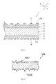
- FIG. 1 is a cross-sectional view of a solar cell manufactured in a first embodiment. The configuration of the solar cell manufactured in this embodiment will be explained first with reference to FIG. 1 .
- the solar cell 1 includes a crystalline silicon substrate 10.
- the crystalline silicon substrate 10 can be a single-crystal silicon substrate or a polycrystalline silicon substrate.
- the conductive type of the crystalline silicon substrate 10 is n-type.
- the present invention is not limited to this.
- the conductive type of the crystalline silicon substrate 10 can be p-type.
- a p-type semiconductor layer 11 with a different type of conductivity from the crystalline silicon substrate 10 is arranged on the first main surface 10a of the crystalline silicon substrate 10.
- the p-type semiconductor layer 11 can be made of a p-type amorphous silicon layer.
- the p-type semiconductor layer 11 preferably contains hydrogen.
- the thickness of the p-type semiconductor layer 11 can be from 3 nm to 20 nm, and is preferably from 5 nm to 15 nm.
- the amorphous silicon is a material of a non-crystalline silicon semiconductor material series, and includes the microcrystalline silicon.
- a substantially intrinsic semiconductor layer 12 is arranged between the first main surface 10a of the crystalline silicon substrate 10 and the p-type semiconductor layer 11.
- the substantially intrinsic semiconductor layer 12 can be an i-type amorphous silicon layer.
- the substantially intrinsic semiconductor layer 12 preferably contains hydrogen.
- the substantially intrinsic semiconductor layer 12 is preferably of a thickness that does not contribute substantially to the generation of electricity.
- the thickness of the substantially intrinsic semiconductor layer 12 can be from 3 nm to 15 nm, and is preferably from 5 nm to 10 nm.
- n-type semiconductor layer 13 with the same type of conductivity as the crystalline silicon substrate 10 is arranged on top of the second main surface 10b of the crystalline silicon substrate 10.
- the n-type semiconductor layer 13 can be made of an n-type amorphous silicon layer.
- the n-type semiconductor layer 13 preferably contains hydrogen.
- the thickness of the n-type semiconductor layer 13 can be from 3 nm to 25 nm, and is preferably from 5 nm to 15 nm.
- a substantially intrinsic semiconductor layer 14 is arranged between the second main surface 10b of the crystalline silicon substrate 10 and the n-type semiconductor layer 13.
- the substantially intrinsic semiconductor layer 14 can be an i-type amorphous silicon layer.
- the substantially intrinsic semiconductor layer 14 is preferably of a thickness that does not contribute substantially to the generation of electricity.
- the substantially intrinsic semiconductor layer 14 preferably contains hydrogen.
- the thickness of the substantially intrinsic semiconductor layer 14 can be from 3 nm to 15 nm, and is preferably from 5 nm to 10 nm.
- Transparent conductive oxide (TCO) layers 15 and 16 are arranged on the semiconductor layers 11 and 13.
- a p-side collector electrode 17 is arranged on the TCO layer 15. Holes are collected by the p-side collector electrode 17.
- an n-side collector electrode 18 is arranged on the TCO layer 16. Electrons are collected by the n-side collector electrode 18.
- a crystalline silicon substrate 10 is prepared.
- the method used to produce the crystalline silicon substrate 10 will be explained below in greater detail.
- substantially intrinsic semiconductor layers 12 and 14 are formed on the crystalline silicon substrate 10.
- the substantially intrinsic semiconductor layers 12 and 14 can be formed using a deposition method such the sputtering method or chemical vapor deposition (CVD).
- a p-type semiconductor layer 11 is formed on substantially intrinsic semiconductor layer 12, and an n-type semiconductor layer 13 is formed on substantially intrinsic semiconductor layer 14.
- the p-type semiconductor layer 11 and the n-type semiconductor layer 13 can be formed using a deposition method such the sputtering method or chemical vapor deposition (CVD).
- TCO layers 15 and 16 are formed on the semiconductor layers 11 and 13.
- the TCO layers 15 and 16 can be formed using a deposition method such the sputtering method or chemical vapor deposition (CVD).
- the solar cell 1 is then completed by forming the p-side collector electrode 17 and the n-side collector electrode 18.
- the p-side collector electrode 17 and the n-side collector electrode 18 can be formed by applying conductive paste or by using a plating method.
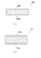
- FIG. 2 is a cross-sectional view of a portion of a crystalline silicon substrate prior to etching.
- FIG. 3 is a cross-sectional view of a portion of a crystalline silicon substrate after the second etching step.
- FIG. 4 is a cross-sectional view of a portion of a crystalline silicon substrate after the third etching step.
- an ingot of crystalline silicon is prepared.
- an ingot of single-crystalline silicon is prepared when a single-crystal silicon substrate is to be produced.
- the ingot of crystalline silicon can be prepared using any method common in the art.
- the ingot of crystalline silicon is sliced using, for example, a wire saw.
- the crystalline silicon substrate 10A shown in FIG. 2 is obtained.
- the crystalline silicon substrate 10A is produced by cutting the ingot in this way.
- the main surfaces 10A1, 10A2 of the crystalline silicon substrate 10A have irregular shapes referred to as saw marks.
- the first and second etching steps are performed on the crystalline silicon substrate 10A. More specifically, in both the first and the second etching steps, the unevenness of the main surfaces 10A1 and 10A2 of the crystalline silicon substrate 10A is removed and the main surfaces 10A1 and 10A2 are substantially smoothed by immersing the crystalline silicon substrate 10A in an etching solution. This produces the crystalline silicon substrate 10B with smooth main surfaces 10B1 and 10B2 as shown in FIG. 3 .
- the main surfaces 10B1 and 10B2 do not have to be completely smooth, but should at least have a degree of smoothness higher than main surfaces 10A1 and 10A2.
- the first etching step and second etching step do not have to be pure isotropic etching steps. They only have to be substantially isotropic etching steps.
- isotropic etching is performed on the main surfaces 10A1 and 10A2 of the crystalline silicon substrate 10A by immersing the crystalline silicon substrate 10A in an etching solution (first etching solution).
- isotropic etching is again performed on the main surfaces 10A1 and 10A2 of the crystalline silicon substrate 10A by immersing the crystalline silicon substrate 10A in an etching solution (second etching solution) different from the first etching solution used in the first etching step.
- the main surfaces 10A1 and 10A2 of the crystalline silicon substrate 10A are removed and the main surfaces 10A1 and 10A2 are smoothed to a certain degree. For this reason, the main surfaces 10A1 and 10A2 do not have to be etched with high shaping precision.
- the main surfaces 10A1 and 10A2 smoothed to a certain degree in the first etching step are etched to a sufficient degree of smoothness.
- the etching rate in the first etching step is relatively high, and the etching rate in the second etching step is relatively low. In this way, the amount of time required for the first and second etching steps is reduced, and the resulting crystalline silicon substrate 10B has main surfaces 10B1 and 10B2 with a high degree of smoothness.
- the first etching step does not have to be performed.
- the second etching step may be performed alone. This can remove organic matter and smooth the main surfaces 10A1 and 10A2. However, when only the second etching step, which has a low etching rate, is performed to remove the organic matter and smooth out the main surfaces 10A1 and 10A2, the time required in the etching process to achieve the target smoothness is lengthy.
- the first and second etching solutions can be alkaline solutions, such as aqueous solutions containing sodium hydroxide and/or potassium hydroxide.
- the first etching solution and the second etching solution can be the same type of etching solution or different types of etching solutions.
- concentration of etching components in the first and second etching solutions sodium hydroxide, potassium hydroxide, etc.
- concentration of etching components in the first etching solution may be lower than, identical to, or higher than the concentration of etching components in the second etching solution.
- the etching components in the first etching step more readily etch the substrate than the etching components in the second etching step.
- the concentration of etching components in the first etching solution used in the first etching step is lower than the concentration of etching components in the second etching solution used in the second etching step, the etching rate in the first etching step is often made higher than the etching rate in the second etching step.
- the concentration of etching components in the first and second etching solutions can be from 2 mass% to 10 mass%.
- the etching times for the first and second etching steps can be determined, as appropriate, according to the thickness of the crystalline silicon substrate 10A to be etched in each etching step.
- the etching time for the first etching step can be the same as the etching time for the second etching step. It can also be shorter or longer than the etching time for the second etching step.
- the etching time for each of the first and second etching steps can be from 1 minute to 15 minutes.
- the temperature for the first etching step can be the same as the temperature for the second etching step. It can also be higher or lower than the temperature for the second etching step.
- the temperature for each of the first and second etching steps can be from room temperature to 95°C.
- the third etching step is performed on the crystalline silicon substrate 10B.
- the third etching step is an anisotropic etching step.
- the third etching step can be performed to complete a crystalline silicon substrate 10 in which the textured structure shown in FIG. 4 is formed on the main surfaces 10a and 10b. Depiction of the textured structure is omitted from the main surfaces 10a and 10b in FIG. 1 .
- a “textured surface” is an uneven surface which is formed to suppress surface reflection and increase the amount of light absorbed by the solar cell substrate.
- the textured surface usually has a plurality of substantially square pyramidal protruding portions.
- the anisotropic etching step utilizes a phenomenon in which, when a silicon crystal has different crystal planes, the etching rates thereof are also different. More specifically, when an alkaline aqueous solution is used as the etching solution, the etching rate is fastest for the (100) plane of the silicon crystal, and is slowest for the (111) plane. For this reason, when a (111) plane which has a slow etching rate occurs while performing the anisotropic etching step on a crystalline silicon substrate 10B in which a (100) plane is exposed, etching of the (100) plane is given priority. As a result, square pyramidal protrusions are formed by the (111) plane and a crystal plane equivalent to the (111) plane. This phenomenon forms a textured structure. The (111) plane and the crystal plane equivalent to the (111) plane are inclined 54.7° with respect to the (100) plane.
- the crystalline silicon substrate 10B is etched using a third etching solution which has a higher etching component concentration than the second etching solution used in the second etching step or isotropic etching step.
- the etching is performed at an etching rate that is lower than the etching rate in the second etching step.
- the dimensional discrepancies between the protrusions constituting the textured structure can be reduced.
- a solar cell 1 with excellent output characteristics can be manufactured with greater efficiency. In other words, the time required to manufacture a solar cell 1 with excellent output characteristics can be reduced.
- the reason for this is not clear, but is thought to be due to the following.
- the formation of a textured structure requires base points (a trigger which starts anisotropic etching due to the difference between both points).
- the base points In order to form a textured structure with a uniform size, the base points have to be formed on the wafer surface at as close to the same time as possible. In other words, it is believed that the base points can be formed at the same time by smoothing out the plane in the first etching step, which is an isotropic etching step, and then forming the base points in the second etching step, which is an anisotropic etching step.
- the textured structure is formed immediately after the base points have been formed, and the time at which the anisotropic etching begins varies in the plane.
- the etching rate is fast, even when there is a slight difference in the time at which the anisotropic etching starts there is not a significant difference in the amount of etching performed on the plane. This is believed to form a relatively uniform textured structure.
- the ratio of the etching rate for the third etching solution used in the third etching step to the etching rate for the second etching solution used in the second etching step should be in a range from 0.10 to 0.95, and is preferably from 0.50 to 0.80.
- the ratio of the concentration of etching components in the third etching solution used in the third etching step to the concentration of etching components in the second etching solution used in the second etching step should be in a range from 1.03 to 1.70, and is preferably from 1.10 to 1.30.
- the temperature of the etching steps can be adjusted so that the etching rate in the third etching step is lower than the etching rate in the second etching step.
- An etching solution containing an additive that reduces the etching rate may also be used as the third etching solution in the third etching step, so as to reduce the etching rate in the third etching step below the etching rate in the second etching rate.
- additives include caprylic acid, lauric acid, 4-propyl benzoic acid (PrBA), 4-t-butyl benzoic acid (TBBA), 4-n-butyl benzoic acid (NBBA), 4-pentyl benzoic acid (PeBA), and 4-n-octyl benzene sulfonic acid (NOBS).
- PrBA 4-propyl benzoic acid
- TBBA 4-t-butyl benzoic acid
- NBBA 4-n-butyl benzoic acid
- PeBA 4-pentyl benzoic acid
- NOBS 4-n-octyl benzene sulfonic acid
- One of these additives may be added to the second etching solution, or multiple kinds of additives may be added to the second etching solution.
- Etching solutions that are preferably used in the third etching step include those containing an alkaline etching component such as an aqueous solution containing sodium hydroxide and/or potassium hydroxide, as well as those containing an additive enabling anisotropic etching.
- PrBA 4-propyl benzoic acid
- TBBA 4-t-butyl benzoic acid
- NBBA 4-n-butyl benzoic acid
- PeBA 4-pentyl benzoic acid
- NOBS 4-n-octyl benzene sulfonic acid
- the etching time for the third etching step can be from 10 minutes to 45 minutes.
- the temperature for the third etching step can be from 70°C to 90°C.
- the solar cell may be a back contact solar cell.
- the solar cell may also be a solar cell including a crystalline silicon substrate on which at least either a p-type dopant diffusion region or a n-type dopant diffusion region has been formed.
- the isotropic etching step was performed twice.
- the isotropic etching step may be performed only once or may be performed three or more times.
- the anisotropic etching step may also be performed two or more times.
- a textured structure does not have to be formed on both main surfaces of the crystalline silicon substrate.
- a textured structure may be formed on only one of the main surfaces of the crystalline silicon substrate.
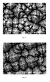
- FIG. 5 is an electron micrograph of a main surface of the single-crystal silicon substrate produced in a first test example.
- the etching rate in the isotropic etching step was 1.5 ⁇ m/min. and the amount of etching was 7 ⁇ m.
- the etching rate in the anisotropic etching step was 1.0 ⁇ m/min. and the amount of etching was 20 ⁇ m.
- Etching Solution Aqueous Solution Containing 4 mass% NaOH
- Etching Solution Aqueous Solution Containing 5 mass% NaOH and 0.05 mol/L caprylic acid
- FIG. 6 is an electron micrograph of a main surface of the single-crystal silicon substrate produced in a second test example.
- the etching rate in the first isotropic etching step was 6 ⁇ m/min. and the amount of etching was 13 ⁇ m.
- the etching rate in the second isotropic etching step was 1.5 ⁇ m/min. and the amount of etching was 7 ⁇ m.
- the etching rate in the anisotropic etching step was 1.0 ⁇ m/min. and the amount of etching was 20 ⁇ m.
- Etching Solution Aqueous Solution Containing 3 mass% NaOH
- Etching Solution Aqueous Solution Containing 4 mass% NaOH
- Etching Solution Aqueous Solution Containing 5 mass% NaOH and 0.05 mol/L caprylic acid
- FIG. 7 is an electron micrograph of a main surface of the single-crystal silicon substrate produced in the comparative example.
- the etching rate in the anisotropic etching step was 1.0 ⁇ m/min. and the amount of etching was 27 ⁇ m.
- Etching Solution Aqueous Solution Containing 16 mass% NaOH and 0.05 mol/L caprylic acid
- the textured structure formed in the comparative example has a small degree of unevenness.
- the textured structures formed in the first and second test examples have a larger degree of unevenness.
- the uniformity of the degree of unevenness in these textured structures is better than that of the comparative example.
Landscapes
- Photovoltaic Devices (AREA)
- Weting (AREA)
Abstract
Description
- The present invention relates to a manufacturing method for a solar cell. More specifically, the present invention relates to a manufacturing method for a solar cell including a crystalline silicon substrate having a main surface in which a textured structure has been formed.
- Interest in solar cells has increased in recent years as an energy source with a low environmental impact.
-
Patent Document 1 and Patent Document 2 describe crystalline silicon solar cells using a crystalline silicon substrate. In the crystalline silicon solar cells described in -
Patent Document 1 and Patent Document 2, an uneven structure referred to as a textured structure is formed on the surface of the crystalline silicon substrate to increase the incident efficiency of the light on the crystalline silicon substrate. - Patent Document 2 describes the following method of forming a textured structure in a single-crystal silicon substrate. In the first step, the single-crystal silicon substrate is immersed in a 5 mass% sodium hydroxide aqueous solution for ten minutes at approximately 85°C. The first step removes the processing strain on the surface of the single-crystal silicon substrate. In the second step, anisotropic etching is performed on the surface of the single-crystal silicon using an aqueous solution containing approximately 2 mass% sodium hydroxide and isopropyl alcohol. Here, the concentration of sodium hydroxide is lower than in the first step. In the second step, a pyramidal textured structure is formed on the surface of the single-crystal silicon substrate. In other words, in Patent Document 2, a textured structure is formed by performing isotropic etching using an etching solution containing a relatively high concentration of etchant, and then performing anisotropic etching using an etching solution containing a relatively low concentration of etchant.
-
- Patent Document 1: Laid-Open Patent Publication No. 11-220146
- Patent Document 2:
PCT Laid-Open Patent Publication No. WO98/43304 - A precisely shaped textured structure cannot be formed in a short period of time using the textured structure forming method described in Patent Document 2. As a result, it takes longer to manufacture a solar cell.
- In view of this situation, it is a purpose of the present invention to reduce the time required to manufacture a solar cell.
- The present invention is a manufacturing method for a solar cell including a crystalline silicon substrate having a main surface in which a textured structure has been formed. In the manufacturing method for a solar cell in the present invention, the textured structure is formed on the main surface of the crystalline silicon substrate by etching the main surface of the crystalline silicon substrate using one etching solution, and then etching the main surface of the crystalline silicon substrate at a lower etching rate than the etching performed using the one etching solution by using another etching solution having a higher concentration of etching components than the one etching solution.
- The present invention is able to reduce the time required to manufacture a solar cell.
-
-
FIG. 1 is a cross-sectional view of a solar cell manufactured in a first embodiment. -
FIG. 2 is a cross-sectional view of a portion of a crystalline silicon substrate prior to etching. -
FIG. 3 is a cross-sectional view of a portion of a crystalline silicon substrate after the second etching step. -
FIG. 4 is a cross-sectional view of a portion of a crystalline silicon substrate after the third etching step. -
FIG. 5 is an electron micrograph of a main surface of the single-crystal silicon substrate produced in a first test example. -
FIG. 6 is an electron micrograph of a main surface of the single-crystal silicon substrate produced in a second test example. -
FIG. 7 is an electron micrograph of a main surface of the single-crystal silicon substrate produced in a comparative example. - The following is an explanation of an example of a preferred embodiment of the present invention. The following embodiment is merely an example. The present invention is not limited to the following embodiment in any way.
- Further, in each of the drawings referenced in the embodiment, members having substantially the same function are denoted by the same symbols. The drawings referenced in the embodiment are also depicted schematically. The dimensional ratios of the objects depicted in the drawings may differ from those of the actual objects. The dimensional ratios of objects may also vary between drawings. The specific dimensional ratios of the objects should be determined with reference to the following explanation.
-
FIG. 1 is a cross-sectional view of a solar cell manufactured in a first embodiment. The configuration of the solar cell manufactured in this embodiment will be explained first with reference toFIG. 1 . - The
solar cell 1 includes acrystalline silicon substrate 10. Thecrystalline silicon substrate 10 can be a single-crystal silicon substrate or a polycrystalline silicon substrate. In the explanation of present embodiment, the conductive type of thecrystalline silicon substrate 10 is n-type. However, the present invention is not limited to this. The conductive type of thecrystalline silicon substrate 10 can be p-type. - A p-
type semiconductor layer 11 with a different type of conductivity from thecrystalline silicon substrate 10 is arranged on the firstmain surface 10a of thecrystalline silicon substrate 10. The p-type semiconductor layer 11 can be made of a p-type amorphous silicon layer. The p-type semiconductor layer 11 preferably contains hydrogen. The thickness of the p-type semiconductor layer 11 can be from 3 nm to 20 nm, and is preferably from 5 nm to 15 nm. The amorphous silicon is a material of a non-crystalline silicon semiconductor material series, and includes the microcrystalline silicon. - A substantially
intrinsic semiconductor layer 12 is arranged between the firstmain surface 10a of thecrystalline silicon substrate 10 and the p-type semiconductor layer 11. The substantiallyintrinsic semiconductor layer 12 can be an i-type amorphous silicon layer. The substantiallyintrinsic semiconductor layer 12 preferably contains hydrogen. The substantiallyintrinsic semiconductor layer 12 is preferably of a thickness that does not contribute substantially to the generation of electricity. The thickness of the substantiallyintrinsic semiconductor layer 12 can be from 3 nm to 15 nm, and is preferably from 5 nm to 10 nm. - An n-
type semiconductor layer 13 with the same type of conductivity as thecrystalline silicon substrate 10 is arranged on top of the secondmain surface 10b of thecrystalline silicon substrate 10. The n-type semiconductor layer 13 can be made of an n-type amorphous silicon layer. The n-type semiconductor layer 13 preferably contains hydrogen. The thickness of the n-type semiconductor layer 13 can be from 3 nm to 25 nm, and is preferably from 5 nm to 15 nm. - A substantially
intrinsic semiconductor layer 14 is arranged between the secondmain surface 10b of thecrystalline silicon substrate 10 and the n-type semiconductor layer 13. The substantiallyintrinsic semiconductor layer 14 can be an i-type amorphous silicon layer. The substantiallyintrinsic semiconductor layer 14 is preferably of a thickness that does not contribute substantially to the generation of electricity. The substantiallyintrinsic semiconductor layer 14 preferably contains hydrogen. The thickness of the substantiallyintrinsic semiconductor layer 14 can be from 3 nm to 15 nm, and is preferably from 5 nm to 10 nm. - Transparent conductive oxide (TCO) layers 15 and 16 are arranged on the semiconductor layers 11 and 13. A p-
side collector electrode 17 is arranged on theTCO layer 15. Holes are collected by the p-side collector electrode 17. Meanwhile, an n-side collector electrode 18 is arranged on theTCO layer 16. Electrons are collected by the n-side collector electrode 18. - The following is an explanation of an example of the manufacturing method for a
solar cell 1. - First, a
crystalline silicon substrate 10 is prepared. The method used to produce thecrystalline silicon substrate 10 will be explained below in greater detail. - Next, substantially intrinsic semiconductor layers 12 and 14 are formed on the
crystalline silicon substrate 10. The substantially intrinsic semiconductor layers 12 and 14 can be formed using a deposition method such the sputtering method or chemical vapor deposition (CVD). - Next, a p-
type semiconductor layer 11 is formed on substantiallyintrinsic semiconductor layer 12, and an n-type semiconductor layer 13 is formed on substantiallyintrinsic semiconductor layer 14. The p-type semiconductor layer 11 and the n-type semiconductor layer 13 can be formed using a deposition method such the sputtering method or chemical vapor deposition (CVD). - Next, TCO layers 15 and 16 are formed on the semiconductor layers 11 and 13. The TCO layers 15 and 16 can be formed using a deposition method such the sputtering method or chemical vapor deposition (CVD).
- The
solar cell 1 is then completed by forming the p-side collector electrode 17 and the n-side collector electrode 18. The p-side collector electrode 17 and the n-side collector electrode 18 can be formed by applying conductive paste or by using a plating method. -
FIG. 2 is a cross-sectional view of a portion of a crystalline silicon substrate prior to etching.FIG. 3 is a cross-sectional view of a portion of a crystalline silicon substrate after the second etching step.FIG. 4 is a cross-sectional view of a portion of a crystalline silicon substrate after the third etching step. - The following is a detailed explanation of the method used to produce the
crystalline silicon substrate 10 with reference primarily toFIG. 2 through FIG. 4 . - First, an ingot of crystalline silicon is prepared. For example, an ingot of single-crystalline silicon is prepared when a single-crystal silicon substrate is to be produced. The ingot of crystalline silicon can be prepared using any method common in the art.
- Next, the ingot of crystalline silicon is sliced using, for example, a wire saw. Thus, the
crystalline silicon substrate 10A shown inFIG. 2 is obtained. Thecrystalline silicon substrate 10A is produced by cutting the ingot in this way. As a result, the main surfaces 10A1, 10A2 of thecrystalline silicon substrate 10A have irregular shapes referred to as saw marks. - Next, the first and second etching steps are performed on the
crystalline silicon substrate 10A. More specifically, in both the first and the second etching steps, the unevenness of the main surfaces 10A1 and 10A2 of thecrystalline silicon substrate 10A is removed and the main surfaces 10A1 and 10A2 are substantially smoothed by immersing thecrystalline silicon substrate 10A in an etching solution. This produces thecrystalline silicon substrate 10B with smooth main surfaces 10B1 and 10B2 as shown inFIG. 3 . The main surfaces 10B1 and 10B2 do not have to be completely smooth, but should at least have a degree of smoothness higher than main surfaces 10A1 and 10A2. The first etching step and second etching step do not have to be pure isotropic etching steps. They only have to be substantially isotropic etching steps. - More specifically, in the first etching step, isotropic etching is performed on the main surfaces 10A1 and 10A2 of the
crystalline silicon substrate 10A by immersing thecrystalline silicon substrate 10A in an etching solution (first etching solution). In the second etching step, isotropic etching is again performed on the main surfaces 10A1 and 10A2 of thecrystalline silicon substrate 10A by immersing thecrystalline silicon substrate 10A in an etching solution (second etching solution) different from the first etching solution used in the first etching step. - In the first etching step, organic matter adhering to the main surfaces 10A1 and 10A2 of the
crystalline silicon substrate 10A are removed and the main surfaces 10A1 and 10A2 are smoothed to a certain degree. For this reason, the main surfaces 10A1 and 10A2 do not have to be etched with high shaping precision. In contrast, in the second etching step, the main surfaces 10A1 and 10A2 smoothed to a certain degree in the first etching step are etched to a sufficient degree of smoothness. - Therefore, the etching rate in the first etching step is relatively high, and the etching rate in the second etching step is relatively low. In this way, the amount of time required for the first and second etching steps is reduced, and the resulting
crystalline silicon substrate 10B has main surfaces 10B1 and 10B2 with a high degree of smoothness. - The first etching step does not have to be performed. The second etching step may be performed alone. This can remove organic matter and smooth the main surfaces 10A1 and 10A2. However, when only the second etching step, which has a low etching rate, is performed to remove the organic matter and smooth out the main surfaces 10A1 and 10A2, the time required in the etching process to achieve the target smoothness is lengthy.
- There are no particular restrictions on the first and second etching solutions as long as the
crystalline silicon substrate 10A can be etched. The first and second etching solutions can be alkaline solutions, such as aqueous solutions containing sodium hydroxide and/or potassium hydroxide. The first etching solution and the second etching solution can be the same type of etching solution or different types of etching solutions. - There are no restrictions on the concentration of etching components in the first and second etching solutions (sodium hydroxide, potassium hydroxide, etc.) as long as the etching rate in the first etching step is higher than the etching rate in the second etching step. The concentration of etching components in the first etching solution may be lower than, identical to, or higher than the concentration of etching components in the second etching solution. Usually, the etching components in the first etching step more readily etch the substrate than the etching components in the second etching step. For this reason, even if the concentration of etching components in the first etching solution used in the first etching step is lower than the concentration of etching components in the second etching solution used in the second etching step, the etching rate in the first etching step is often made higher than the etching rate in the second etching step. The concentration of etching components in the first and second etching solutions can be from 2 mass% to 10 mass%.
- The etching times for the first and second etching steps can be determined, as appropriate, according to the thickness of the
crystalline silicon substrate 10A to be etched in each etching step. The etching time for the first etching step can be the same as the etching time for the second etching step. It can also be shorter or longer than the etching time for the second etching step. The etching time for each of the first and second etching steps can be from 1 minute to 15 minutes. - There are no particular restrictions on the temperatures at which the first and second etching steps are performed. The temperature for the first etching step can be the same as the temperature for the second etching step. It can also be higher or lower than the temperature for the second etching step. The temperature for each of the first and second etching steps can be from room temperature to 95°C.
- Next, the third etching step is performed on the
crystalline silicon substrate 10B. The third etching step is an anisotropic etching step. The third etching step can be performed to complete acrystalline silicon substrate 10 in which the textured structure shown inFIG. 4 is formed on themain surfaces main surfaces FIG. 1 . - Here, a "textured surface" is an uneven surface which is formed to suppress surface reflection and increase the amount of light absorbed by the solar cell substrate. The textured surface usually has a plurality of substantially square pyramidal protruding portions.
- The anisotropic etching step utilizes a phenomenon in which, when a silicon crystal has different crystal planes, the etching rates thereof are also different.. More specifically, when an alkaline aqueous solution is used as the etching solution, the etching rate is fastest for the (100) plane of the silicon crystal, and is slowest for the (111) plane. For this reason, when a (111) plane which has a slow etching rate occurs while performing the anisotropic etching step on a
crystalline silicon substrate 10B in which a (100) plane is exposed, etching of the (100) plane is given priority. As a result, square pyramidal protrusions are formed by the (111) plane and a crystal plane equivalent to the (111) plane. This phenomenon forms a textured structure. The (111) plane and the crystal plane equivalent to the (111) plane are inclined 54.7° with respect to the (100) plane. - In the third etching step or anisotropic etching step, the
crystalline silicon substrate 10B is etched using a third etching solution which has a higher etching component concentration than the second etching solution used in the second etching step or isotropic etching step. In the third etching step, however, the etching is performed at an etching rate that is lower than the etching rate in the second etching step. In this way, a textured structure with high shape precision can be obtained while also reducing the time required to perform both the second and third etching steps. In particular, the dimensional discrepancies between the protrusions constituting the textured structure can be reduced. As a result, asolar cell 1 with excellent output characteristics can be manufactured with greater efficiency. In other words, the time required to manufacture asolar cell 1 with excellent output characteristics can be reduced. - The reason for this is not clear, but is thought to be due to the following. The formation of a textured structure requires base points (a trigger which starts anisotropic etching due to the difference between both points). In order to form a textured structure with a uniform size, the base points have to be formed on the wafer surface at as close to the same time as possible. In other words, it is believed that the base points can be formed at the same time by smoothing out the plane in the first etching step, which is an isotropic etching step, and then forming the base points in the second etching step, which is an anisotropic etching step. When the etching rate is fast, the textured structure is formed immediately after the base points have been formed, and the time at which the anisotropic etching begins varies in the plane. However, when the etching rate is slow, even when there is a slight difference in the time at which the anisotropic etching starts there is not a significant difference in the amount of etching performed on the plane. This is believed to form a relatively uniform textured structure.
- In order to manufacture the
solar cell 1 with even greater efficiency, the ratio of the etching rate for the third etching solution used in the third etching step to the etching rate for the second etching solution used in the second etching step (etching rate for the third etching solution/etching rate of the second etching solution) should be in a range from 0.10 to 0.95, and is preferably from 0.50 to 0.80. - The ratio of the concentration of etching components in the third etching solution used in the third etching step to the concentration of etching components in the second etching solution used in the second etching step (concentration of etching components in the third etching solution/concentration of etching components in the second etching solution) should be in a range from 1.03 to 1.70, and is preferably from 1.10 to 1.30.
- There are no particular restrictions on the method used to reduce the etching rate in the third etching step or anisotropic etching step below the etching rate in the second etching step or isotropic etching step. For example, the temperature of the etching steps can be adjusted so that the etching rate in the third etching step is lower than the etching rate in the second etching step.
- An etching solution containing an additive that reduces the etching rate may also be used as the third etching solution in the third etching step, so as to reduce the etching rate in the third etching step below the etching rate in the second etching rate.
- Specific examples of these additives include caprylic acid, lauric acid, 4-propyl benzoic acid (PrBA), 4-t-butyl benzoic acid (TBBA), 4-n-butyl benzoic acid (NBBA), 4-pentyl benzoic acid (PeBA), and 4-n-octyl benzene sulfonic acid (NOBS). One of these additives may be added to the second etching solution, or multiple kinds of additives may be added to the second etching solution.
- There are no particular restrictions on the etching solution used in the third etching step as long as anisotropic etching can be performed on the
crystalline silicon substrate 10B. Etching solutions that are preferably used in the third etching step include those containing an alkaline etching component such as an aqueous solution containing sodium hydroxide and/or potassium hydroxide, as well as those containing an additive enabling anisotropic etching. Specific examples of additives that enable anisotropic etching include caprylic acid, lauric acid, 4-propyl benzoic acid (PrBA), 4-t-butyl benzoic acid (TBBA), 4-n-butyl benzoic acid (NBBA), 4-pentyl benzoic acid (PeBA), and 4-n-octyl benzene sulfonic acid (NOBS). One or more of these additives may be used. - There are no particular restrictions on the etching time for the third etching step as long as a good textured structure can be formed. The etching time for the third etching step can be from 10 minutes to 45 minutes.
- The temperature for the third etching step can be from 70°C to 90°C.
- In the present invention, there are no particular restrictions on the type of solar cell as long as a crystalline silicon substrate is used. The solar cell may be a back contact solar cell. The solar cell may also be a solar cell including a crystalline silicon substrate on which at least either a p-type dopant diffusion region or a n-type dopant diffusion region has been formed.
- In the embodiment described above, the isotropic etching step was performed twice. However, the present invention is not limited to this configuration. The isotropic etching step may be performed only once or may be performed three or more times. The anisotropic etching step may also be performed two or more times.
- A textured structure does not have to be formed on both main surfaces of the crystalline silicon substrate. A textured structure may be formed on only one of the main surfaces of the crystalline silicon substrate.
- A single-crystal silicon substrate was obtained by slicing an ingot of single-crystal silicon using a wire saw. Next, isotropic etching was performed on the surface of the single-crystal silicon substrate under the conditions mentioned below. Afterwards, anisotropic etching was performed under the conditions mentioned below to form a textured structure.
FIG. 5 is an electron micrograph of a main surface of the single-crystal silicon substrate produced in a first test example. - In the first test example, the etching rate in the isotropic etching step was 1.5 µm/min. and the amount of etching was 7 µm. The etching rate in the anisotropic etching step was 1.0 µm/min. and the amount of etching was 20 µm.
- Etching Solution: Aqueous Solution Containing 4 mass% NaOH
- Temperature of Etching Solution: 75°C
- Etching Time: 270 seconds
- Etching Solution: Aqueous Solution Containing 5 mass% NaOH and 0.05 mol/L caprylic acid
- Temperature of Etching Solution: 85°C
- Etching Time: 1200 seconds
- Isotropic etching was performed twice under the conditions mentioned below on the surface of a single-crystal silicon substrate obtained from a single-crystal silicon ingot in the same manner as the first test example. Afterwards, anisotropic etching was performed under the conditions mentioned below to form a textured structure.
FIG. 6 is an electron micrograph of a main surface of the single-crystal silicon substrate produced in a second test example. - In the second test example, the etching rate in the first isotropic etching step was 6 µm/min. and the amount of etching was 13 µm. The etching rate in the second isotropic etching step was 1.5 µm/min. and the amount of etching was 7 µm. The etching rate in the anisotropic etching step was 1.0 µm/min. and the amount of etching was 20 µm.
- Etching Solution: Aqueous Solution Containing 3 mass% NaOH
- Temperature of Etching Solution: 85°C
- Etching Time: 130 seconds
- Etching Solution: Aqueous Solution Containing 4 mass% NaOH
- Temperature of Etching Solution: 75°C
- Etching Time: 270 seconds
- Etching Solution: Aqueous Solution Containing 5 mass% NaOH and 0.05 mol/L caprylic acid
- Temperature of Etching Solution: 85°C
- Etching Time: 1200 seconds
- A single-crystal silicon substrate was obtained by slicing an ingot of single-crystal silicon using a wire saw. Next, isotropic etching was performed on the surface of the single-crystal silicon substrate under the conditions mentioned above. Afterwards, anisotropic etching was performed under the conditions mentioned below to form a textured structure.
FIG. 7 is an electron micrograph of a main surface of the single-crystal silicon substrate produced in the comparative example. - In the first test example, the etching rate in the anisotropic etching step was 1.0 µm/min. and the amount of etching was 27 µm.
- Etching Solution: Aqueous Solution Containing 16 mass% NaOH and 0.05 mol/L caprylic acid
- Temperature of Etching Solution: 85°C
- Etching Time: 1620 seconds
- As shown in the electron micrograph of a main surface of the single-crystal silicon substrate in
FIG. 7 , the textured structure formed in the comparative example has a small degree of unevenness. However, as shown in the electron micrographs of a main surface of single-crystal silicon substrates inFIG. 5 and FIG. 6 , the textured structures formed in the first and second test examples have a larger degree of unevenness. In addition to a larger degree of unevenness, the uniformity of the degree of unevenness in these textured structures is better than that of the comparative example. -
- 1:
- Solar cell
- 10:
- Crystalline silicon substrate
- 10A:
- Crystalline silicon substrate prior to etching
- 10B:
- Crystalline silicon substrate after isotropic etching
- 10a
- 1st main surface
- 10b:
- 2nd main surface
- 11:
- p-type semiconductor layer
- 12, 14:
- Substantially intrinsic semiconductor layer
- 13:
- n-type semiconductor layer
- 15, 16:
- TCO layer
- 17:
- p-side collector electrode
- 18:
- n-side collector electrode
Claims (10)
- A manufacturing method for a solar cell including a crystalline silicon substrate having a main surface in which a textured structure has been formed,
the textured structure being formed in the main surface of the crystalline silicon substrate by etching the main surface of the crystalline silicon substrate using one etching solution, and then etching the main surface of the crystalline silicon substrate at a lower etching rate than the etching performed using the one etching solution by using another etching solution having a higher concentration of etching components than the one etching solution. - The manufacturing method for a solar cell according to claim 1, wherein the etching rate for the other etching solution is reduced below the etching rate for the one etching solution by using, as the other etching solution, an etching solution including an additive for reducing the etching rate.
- The manufacturing method for a solar cell according to claim 2, wherein the other etching solution is an etching solution containing, as the additive, at least one of caprylic acid, lauric acid, 4-propyl benzoic acid, 4-t-butyl benzoic acid, 4-n-butyl benzoic acid, 4-pentyl benzoic acid, and 4-n-octyl benzene sulfonic acid.
- The manufacturing method for a solar cell according to any one of claims 1 through 3, wherein isotropic etching is performed on the main surface of the crystalline silicon substrate using the one etching solution, and anisotropic etching is performed on the main surface of the crystalline silicon substrate using the other etching solution.
- The manufacturing method for a solar cell according to any one of claims 1 through 4, wherein prior to the etching performed using the one etching solution, etching is performed on the main surface of the crystalline silicon substrate at a higher etching rate than the etching performed using the one etching solution.
- The manufacturing method for a solar cell according to any one of claims 1 through 5, wherein alkaline etching solutions are used for both the one etching solution and the other etching solution.
- The manufacturing method for a solar cell according to claim 6, wherein aqueous solutions containing sodium hydroxide and/or potassium hydroxide are used for both the one etching solution and the other etching solution.
- The manufacturing method for a solar cell according to any one of claims 1 through 7, wherein the ratio of the etching rate for the other etching solution to the etching rate for the one etching solution (etching rate for the other etching solution/etching rate of the one etching solution) is in a range from 0.10 to 0.95.
- The manufacturing method for a solar cell according to any one of claims 1 through 8, wherein the ratio of the concentration of etching components in the other etching solution to the concentration of etching components in the one etching solution (concentration of etching components in the other etching solution/concentration of etching components in the one etching solution) is in a range from 1.03 to 1.70.
- The manufacturing method for a solar cell according to any one of claims 1 through 9, wherein a single-crystal silicon substrate or polycrystalline silicon substrate is used as the crystalline silicon substrate.
Applications Claiming Priority (2)
| Application Number | Priority Date | Filing Date | Title |
|---|---|---|---|
| JP2011124936 | 2011-06-03 | ||
| PCT/JP2012/063312 WO2012165288A1 (en) | 2011-06-03 | 2012-05-24 | Method for manufacturing solar cell |
Publications (3)
| Publication Number | Publication Date |
|---|---|
| EP2717321A1 true EP2717321A1 (en) | 2014-04-09 |
| EP2717321A4 EP2717321A4 (en) | 2015-05-06 |
| EP2717321B1 EP2717321B1 (en) | 2020-07-29 |
Family
ID=47259145
Family Applications (1)
| Application Number | Title | Priority Date | Filing Date |
|---|---|---|---|
| EP12792011.4A Not-in-force EP2717321B1 (en) | 2011-06-03 | 2012-05-24 | Method for manufacturing solar cell |
Country Status (5)
| Country | Link |
|---|---|
| US (1) | US8835210B2 (en) |
| EP (1) | EP2717321B1 (en) |
| JP (1) | JP6160959B2 (en) |
| CN (1) | CN103597604B (en) |
| WO (1) | WO2012165288A1 (en) |
Families Citing this family (3)
| Publication number | Priority date | Publication date | Assignee | Title |
|---|---|---|---|---|
| US9837259B2 (en) * | 2014-08-29 | 2017-12-05 | Sunpower Corporation | Sequential etching treatment for solar cell fabrication |
| JP2017536692A (en) * | 2014-10-31 | 2017-12-07 | ビーコ プリジション サーフェイス プロセシング エルエルシー | Apparatus and method for performing a wet etch process |
| WO2018145699A2 (en) * | 2017-02-09 | 2018-08-16 | RENA Technologies GmbH | Method for texturing a surface of a semiconductor material and device for carrying out the method |
Family Cites Families (13)
| Publication number | Priority date | Publication date | Assignee | Title |
|---|---|---|---|---|
| AU6420398A (en) * | 1997-03-21 | 1998-10-20 | Sanyo Electric Co., Ltd. | Photovoltaic element and method for manufacture thereof |
| JP3772456B2 (en) * | 1997-04-23 | 2006-05-10 | 三菱電機株式会社 | Solar cell, method for manufacturing the same, and semiconductor manufacturing apparatus |
| JP3377931B2 (en) * | 1997-06-26 | 2003-02-17 | 京セラ株式会社 | Solar cell element |
| JP3602323B2 (en) * | 1998-01-30 | 2004-12-15 | 三菱電機株式会社 | Solar cell manufacturing method |
| JP2000323736A (en) * | 1999-05-10 | 2000-11-24 | Mitsubishi Electric Corp | Manufacturing method of silicon solar cell |
| JP3948890B2 (en) * | 2000-08-09 | 2007-07-25 | 三洋電機株式会社 | Method for manufacturing concavo-convex substrate, surfactant for forming concavo-convex structure, and method for manufacturing photovoltaic element |
| JP2006278409A (en) * | 2005-03-28 | 2006-10-12 | Sanyo Electric Co Ltd | Etching device, manufacturing method of texture substrate, and manufacturing method of photovoltaic device |
| JP2006294696A (en) * | 2005-04-06 | 2006-10-26 | Sharp Corp | Manufacturing method of solar cell and silicon substrate for solar cell |
| JP4326545B2 (en) * | 2006-02-23 | 2009-09-09 | 三洋電機株式会社 | Method for manufacturing concavo-convex substrate and method for manufacturing photovoltaic device |
| US8652869B2 (en) * | 2009-03-25 | 2014-02-18 | Mitsubishi Electric Corporation | Method for roughening substrate surface and method for manufacturing photovoltaic device |
| US20120006790A1 (en) * | 2009-03-31 | 2012-01-12 | Kurita Water Industries Ltd. | Apparatus and method for treating etching solution |
| WO2011048656A1 (en) * | 2009-10-19 | 2011-04-28 | 三菱電機株式会社 | Method for roughening substrate surface, and method for manufacturing photovoltaic device |
| US20120160296A1 (en) * | 2011-09-30 | 2012-06-28 | Olivier Laparra | Textured photovoltaic cells and methods |
-
2012
- 2012-05-24 JP JP2013518013A patent/JP6160959B2/en not_active Expired - Fee Related
- 2012-05-24 EP EP12792011.4A patent/EP2717321B1/en not_active Not-in-force
- 2012-05-24 WO PCT/JP2012/063312 patent/WO2012165288A1/en not_active Ceased
- 2012-05-24 CN CN201280027090.2A patent/CN103597604B/en not_active Expired - Fee Related
-
2013
- 2013-11-27 US US14/091,983 patent/US8835210B2/en not_active Expired - Fee Related
Also Published As
| Publication number | Publication date |
|---|---|
| WO2012165288A1 (en) | 2012-12-06 |
| EP2717321A4 (en) | 2015-05-06 |
| JPWO2012165288A1 (en) | 2015-02-23 |
| US8835210B2 (en) | 2014-09-16 |
| EP2717321B1 (en) | 2020-07-29 |
| JP6160959B2 (en) | 2017-07-12 |
| CN103597604A (en) | 2014-02-19 |
| CN103597604B (en) | 2016-01-20 |
| US20140080246A1 (en) | 2014-03-20 |
Similar Documents
| Publication | Publication Date | Title |
|---|---|---|
| TW201308420A (en) | Solar cell wafer, solar cell and method of manufacturing same | |
| EP3050120B1 (en) | Nanostructured silicon based solar cells and methods to produce nanostructured silicon based solar cells | |
| US8852981B2 (en) | Electrical contacts to nanostructured areas | |
| US10181405B2 (en) | Method for selective under-etching of porous silicon | |
| JP6091458B2 (en) | Photoelectric conversion device and manufacturing method thereof | |
| JP2014511038A (en) | Manufacturing method of solar cell | |
| Rao et al. | A novel low cost 25μm thin exfoliated monocrystalline Si solar cell technology | |
| US8835210B2 (en) | Manufacturing method for solar cell | |
| JP5817046B2 (en) | Manufacturing method of back contact type crystalline silicon solar cell | |
| CN103201847A (en) | Solar cell and manufacturing method thereof | |
| US9935216B2 (en) | Wafer for solar cell, method of producing wafer for solar cell, method of producing solar cell, and method of producing solar cell module | |
| JP2011228529A (en) | Solar battery cell and manufacturing method thereof | |
| CN119452759A (en) | Generation of textured surfaces, fabrication of tandem solar cells, and tandem solar cells | |
| JP2012004489A (en) | Silicon wafer, semiconductor device, method for manufacturing silicon wafer and semiconductor device | |
| JP2015122347A (en) | SOLAR CELL, ITS MANUFACTURING METHOD, SOLAR CELL MODULE | |
| JP2012256713A (en) | Manufacturing method of solar cell | |
| JP2014090086A (en) | Method for etching silicon substrate, etchant for silicon substrate, and method for manufacturing solar cell | |
| JP2012256801A (en) | Formation method of texture structure and manufacturing method of solar cell | |
| WO2017007972A1 (en) | High efficiency single crystal silicon solar cell with epitaxially deposited silicon layers with deep junction(s) | |
| KR101359407B1 (en) | Two-Step Wet Texturing Production Method Using Metal Ultra Thin Film | |
| KR101621564B1 (en) | Solar cell and method for texturing substrate for solar cell | |
| KR101429198B1 (en) | Etchant for Texturing Silicon Substrate and Manufacturing Method of High Efficiency Solar Cell Using the Same | |
| CN109716540A (en) | Solar cell, method for manufacturing the same, and solar cell module | |
| CN205810839U (en) | Silica-based heterojunction solaode | |
| Chang et al. | Improved light trapping structure for monocrystalline silicon solar cells |
Legal Events
| Date | Code | Title | Description |
|---|---|---|---|
| PUAI | Public reference made under article 153(3) epc to a published international application that has entered the european phase |
Free format text: ORIGINAL CODE: 0009012 |
|
| 17P | Request for examination filed |
Effective date: 20131212 |
|
| AK | Designated contracting states |
Kind code of ref document: A1 Designated state(s): AL AT BE BG CH CY CZ DE DK EE ES FI FR GB GR HR HU IE IS IT LI LT LU LV MC MK MT NL NO PL PT RO RS SE SI SK SM TR |
|
| DAX | Request for extension of the european patent (deleted) | ||
| RA4 | Supplementary search report drawn up and despatched (corrected) |
Effective date: 20150409 |
|
| RIC1 | Information provided on ipc code assigned before grant |
Ipc: H01L 31/0747 20120101AFI20150401BHEP Ipc: H01L 31/18 20060101ALI20150401BHEP Ipc: H01L 31/0236 20060101ALI20150401BHEP Ipc: H01L 21/306 20060101ALI20150401BHEP |
|
| RAP1 | Party data changed (applicant data changed or rights of an application transferred) |
Owner name: PANASONIC INTELLECTUAL PROPERTY MANAGEMENT CO., LT |
|
| STAA | Information on the status of an ep patent application or granted ep patent |
Free format text: STATUS: EXAMINATION IS IN PROGRESS |
|
| 17Q | First examination report despatched |
Effective date: 20191114 |
|
| GRAP | Despatch of communication of intention to grant a patent |
Free format text: ORIGINAL CODE: EPIDOSNIGR1 |
|
| STAA | Information on the status of an ep patent application or granted ep patent |
Free format text: STATUS: GRANT OF PATENT IS INTENDED |
|
| RIC1 | Information provided on ipc code assigned before grant |
Ipc: H01L 31/0236 20060101AFI20200311BHEP Ipc: H01L 31/0747 20120101ALI20200311BHEP |
|
| INTG | Intention to grant announced |
Effective date: 20200402 |
|
| GRAS | Grant fee paid |
Free format text: ORIGINAL CODE: EPIDOSNIGR3 |
|
| GRAA | (expected) grant |
Free format text: ORIGINAL CODE: 0009210 |
|
| STAA | Information on the status of an ep patent application or granted ep patent |
Free format text: STATUS: THE PATENT HAS BEEN GRANTED |
|
| AK | Designated contracting states |
Kind code of ref document: B1 Designated state(s): AL AT BE BG CH CY CZ DE DK EE ES FI FR GB GR HR HU IE IS IT LI LT LU LV MC MK MT NL NO PL PT RO RS SE SI SK SM TR |
|
| REG | Reference to a national code |
Ref country code: GB Ref legal event code: FG4D |
|
| REG | Reference to a national code |
Ref country code: CH Ref legal event code: EP |
|
| REG | Reference to a national code |
Ref country code: DE Ref legal event code: R096 Ref document number: 602012071498 Country of ref document: DE |
|
| REG | Reference to a national code |
Ref country code: AT Ref legal event code: REF Ref document number: 1296814 Country of ref document: AT Kind code of ref document: T Effective date: 20200815 |
|
| REG | Reference to a national code |
Ref country code: IE Ref legal event code: FG4D |
|
| REG | Reference to a national code |
Ref country code: LT Ref legal event code: MG4D |
|
| REG | Reference to a national code |
Ref country code: NL Ref legal event code: MP Effective date: 20200729 |
|
| REG | Reference to a national code |
Ref country code: AT Ref legal event code: MK05 Ref document number: 1296814 Country of ref document: AT Kind code of ref document: T Effective date: 20200729 |
|
| PG25 | Lapsed in a contracting state [announced via postgrant information from national office to epo] |
Ref country code: ES Free format text: LAPSE BECAUSE OF FAILURE TO SUBMIT A TRANSLATION OF THE DESCRIPTION OR TO PAY THE FEE WITHIN THE PRESCRIBED TIME-LIMIT Effective date: 20200729 Ref country code: NO Free format text: LAPSE BECAUSE OF FAILURE TO SUBMIT A TRANSLATION OF THE DESCRIPTION OR TO PAY THE FEE WITHIN THE PRESCRIBED TIME-LIMIT Effective date: 20201029 Ref country code: BG Free format text: LAPSE BECAUSE OF FAILURE TO SUBMIT A TRANSLATION OF THE DESCRIPTION OR TO PAY THE FEE WITHIN THE PRESCRIBED TIME-LIMIT Effective date: 20201029 Ref country code: AT Free format text: LAPSE BECAUSE OF FAILURE TO SUBMIT A TRANSLATION OF THE DESCRIPTION OR TO PAY THE FEE WITHIN THE PRESCRIBED TIME-LIMIT Effective date: 20200729 Ref country code: LT Free format text: LAPSE BECAUSE OF FAILURE TO SUBMIT A TRANSLATION OF THE DESCRIPTION OR TO PAY THE FEE WITHIN THE PRESCRIBED TIME-LIMIT Effective date: 20200729 Ref country code: GR Free format text: LAPSE BECAUSE OF FAILURE TO SUBMIT A TRANSLATION OF THE DESCRIPTION OR TO PAY THE FEE WITHIN THE PRESCRIBED TIME-LIMIT Effective date: 20201030 Ref country code: HR Free format text: LAPSE BECAUSE OF FAILURE TO SUBMIT A TRANSLATION OF THE DESCRIPTION OR TO PAY THE FEE WITHIN THE PRESCRIBED TIME-LIMIT Effective date: 20200729 Ref country code: FI Free format text: LAPSE BECAUSE OF FAILURE TO SUBMIT A TRANSLATION OF THE DESCRIPTION OR TO PAY THE FEE WITHIN THE PRESCRIBED TIME-LIMIT Effective date: 20200729 Ref country code: SE Free format text: LAPSE BECAUSE OF FAILURE TO SUBMIT A TRANSLATION OF THE DESCRIPTION OR TO PAY THE FEE WITHIN THE PRESCRIBED TIME-LIMIT Effective date: 20200729 Ref country code: PT Free format text: LAPSE BECAUSE OF FAILURE TO SUBMIT A TRANSLATION OF THE DESCRIPTION OR TO PAY THE FEE WITHIN THE PRESCRIBED TIME-LIMIT Effective date: 20201130 |
|
| PG25 | Lapsed in a contracting state [announced via postgrant information from national office to epo] |
Ref country code: LV Free format text: LAPSE BECAUSE OF FAILURE TO SUBMIT A TRANSLATION OF THE DESCRIPTION OR TO PAY THE FEE WITHIN THE PRESCRIBED TIME-LIMIT Effective date: 20200729 Ref country code: RS Free format text: LAPSE BECAUSE OF FAILURE TO SUBMIT A TRANSLATION OF THE DESCRIPTION OR TO PAY THE FEE WITHIN THE PRESCRIBED TIME-LIMIT Effective date: 20200729 Ref country code: PL Free format text: LAPSE BECAUSE OF FAILURE TO SUBMIT A TRANSLATION OF THE DESCRIPTION OR TO PAY THE FEE WITHIN THE PRESCRIBED TIME-LIMIT Effective date: 20200729 Ref country code: IS Free format text: LAPSE BECAUSE OF FAILURE TO SUBMIT A TRANSLATION OF THE DESCRIPTION OR TO PAY THE FEE WITHIN THE PRESCRIBED TIME-LIMIT Effective date: 20201129 |
|
| PG25 | Lapsed in a contracting state [announced via postgrant information from national office to epo] |
Ref country code: NL Free format text: LAPSE BECAUSE OF FAILURE TO SUBMIT A TRANSLATION OF THE DESCRIPTION OR TO PAY THE FEE WITHIN THE PRESCRIBED TIME-LIMIT Effective date: 20200729 |
|
| PG25 | Lapsed in a contracting state [announced via postgrant information from national office to epo] |
Ref country code: RO Free format text: LAPSE BECAUSE OF FAILURE TO SUBMIT A TRANSLATION OF THE DESCRIPTION OR TO PAY THE FEE WITHIN THE PRESCRIBED TIME-LIMIT Effective date: 20200729 Ref country code: SM Free format text: LAPSE BECAUSE OF FAILURE TO SUBMIT A TRANSLATION OF THE DESCRIPTION OR TO PAY THE FEE WITHIN THE PRESCRIBED TIME-LIMIT Effective date: 20200729 Ref country code: EE Free format text: LAPSE BECAUSE OF FAILURE TO SUBMIT A TRANSLATION OF THE DESCRIPTION OR TO PAY THE FEE WITHIN THE PRESCRIBED TIME-LIMIT Effective date: 20200729 Ref country code: CZ Free format text: LAPSE BECAUSE OF FAILURE TO SUBMIT A TRANSLATION OF THE DESCRIPTION OR TO PAY THE FEE WITHIN THE PRESCRIBED TIME-LIMIT Effective date: 20200729 Ref country code: DK Free format text: LAPSE BECAUSE OF FAILURE TO SUBMIT A TRANSLATION OF THE DESCRIPTION OR TO PAY THE FEE WITHIN THE PRESCRIBED TIME-LIMIT Effective date: 20200729 Ref country code: IT Free format text: LAPSE BECAUSE OF FAILURE TO SUBMIT A TRANSLATION OF THE DESCRIPTION OR TO PAY THE FEE WITHIN THE PRESCRIBED TIME-LIMIT Effective date: 20200729 |
|
| REG | Reference to a national code |
Ref country code: DE Ref legal event code: R097 Ref document number: 602012071498 Country of ref document: DE |
|
| PG25 | Lapsed in a contracting state [announced via postgrant information from national office to epo] |
Ref country code: AL Free format text: LAPSE BECAUSE OF FAILURE TO SUBMIT A TRANSLATION OF THE DESCRIPTION OR TO PAY THE FEE WITHIN THE PRESCRIBED TIME-LIMIT Effective date: 20200729 |
|
| PLBE | No opposition filed within time limit |
Free format text: ORIGINAL CODE: 0009261 |
|
| STAA | Information on the status of an ep patent application or granted ep patent |
Free format text: STATUS: NO OPPOSITION FILED WITHIN TIME LIMIT |
|
| PG25 | Lapsed in a contracting state [announced via postgrant information from national office to epo] |
Ref country code: SK Free format text: LAPSE BECAUSE OF FAILURE TO SUBMIT A TRANSLATION OF THE DESCRIPTION OR TO PAY THE FEE WITHIN THE PRESCRIBED TIME-LIMIT Effective date: 20200729 |
|
| 26N | No opposition filed |
Effective date: 20210430 |
|
| PGFP | Annual fee paid to national office [announced via postgrant information from national office to epo] |
Ref country code: DE Payment date: 20210520 Year of fee payment: 10 |
|
| PG25 | Lapsed in a contracting state [announced via postgrant information from national office to epo] |
Ref country code: SI Free format text: LAPSE BECAUSE OF FAILURE TO SUBMIT A TRANSLATION OF THE DESCRIPTION OR TO PAY THE FEE WITHIN THE PRESCRIBED TIME-LIMIT Effective date: 20200729 |
|
| REG | Reference to a national code |
Ref country code: CH Ref legal event code: PL |
|
| GBPC | Gb: european patent ceased through non-payment of renewal fee |
Effective date: 20210524 |
|
| PG25 | Lapsed in a contracting state [announced via postgrant information from national office to epo] |
Ref country code: CH Free format text: LAPSE BECAUSE OF NON-PAYMENT OF DUE FEES Effective date: 20210531 Ref country code: LU Free format text: LAPSE BECAUSE OF NON-PAYMENT OF DUE FEES Effective date: 20210524 Ref country code: MC Free format text: LAPSE BECAUSE OF FAILURE TO SUBMIT A TRANSLATION OF THE DESCRIPTION OR TO PAY THE FEE WITHIN THE PRESCRIBED TIME-LIMIT Effective date: 20200729 Ref country code: LI Free format text: LAPSE BECAUSE OF NON-PAYMENT OF DUE FEES Effective date: 20210531 |
|
| REG | Reference to a national code |
Ref country code: BE Ref legal event code: MM Effective date: 20210531 |
|
| PG25 | Lapsed in a contracting state [announced via postgrant information from national office to epo] |
Ref country code: IE Free format text: LAPSE BECAUSE OF NON-PAYMENT OF DUE FEES Effective date: 20210524 Ref country code: GB Free format text: LAPSE BECAUSE OF NON-PAYMENT OF DUE FEES Effective date: 20210524 |
|
| PG25 | Lapsed in a contracting state [announced via postgrant information from national office to epo] |
Ref country code: FR Free format text: LAPSE BECAUSE OF NON-PAYMENT OF DUE FEES Effective date: 20210531 |
|
| PG25 | Lapsed in a contracting state [announced via postgrant information from national office to epo] |
Ref country code: BE Free format text: LAPSE BECAUSE OF NON-PAYMENT OF DUE FEES Effective date: 20210531 |
|
| REG | Reference to a national code |
Ref country code: DE Ref legal event code: R119 Ref document number: 602012071498 Country of ref document: DE |
|
| PG25 | Lapsed in a contracting state [announced via postgrant information from national office to epo] |
Ref country code: HU Free format text: LAPSE BECAUSE OF FAILURE TO SUBMIT A TRANSLATION OF THE DESCRIPTION OR TO PAY THE FEE WITHIN THE PRESCRIBED TIME-LIMIT; INVALID AB INITIO Effective date: 20120524 Ref country code: DE Free format text: LAPSE BECAUSE OF NON-PAYMENT OF DUE FEES Effective date: 20221201 Ref country code: CY Free format text: LAPSE BECAUSE OF FAILURE TO SUBMIT A TRANSLATION OF THE DESCRIPTION OR TO PAY THE FEE WITHIN THE PRESCRIBED TIME-LIMIT Effective date: 20200729 |
|
| PG25 | Lapsed in a contracting state [announced via postgrant information from national office to epo] |
Ref country code: MK Free format text: LAPSE BECAUSE OF FAILURE TO SUBMIT A TRANSLATION OF THE DESCRIPTION OR TO PAY THE FEE WITHIN THE PRESCRIBED TIME-LIMIT Effective date: 20200729 |
|
| PG25 | Lapsed in a contracting state [announced via postgrant information from national office to epo] |
Ref country code: MT Free format text: LAPSE BECAUSE OF FAILURE TO SUBMIT A TRANSLATION OF THE DESCRIPTION OR TO PAY THE FEE WITHIN THE PRESCRIBED TIME-LIMIT Effective date: 20200729 |
|
| PG25 | Lapsed in a contracting state [announced via postgrant information from national office to epo] |
Ref country code: TR Free format text: LAPSE BECAUSE OF FAILURE TO SUBMIT A TRANSLATION OF THE DESCRIPTION OR TO PAY THE FEE WITHIN THE PRESCRIBED TIME-LIMIT Effective date: 20200729 |