EP2715541B1 - Détection de perturbation de champ de mram et rétablissement - Google Patents
Détection de perturbation de champ de mram et rétablissement Download PDFInfo
- Publication number
- EP2715541B1 EP2715541B1 EP12792839.8A EP12792839A EP2715541B1 EP 2715541 B1 EP2715541 B1 EP 2715541B1 EP 12792839 A EP12792839 A EP 12792839A EP 2715541 B1 EP2715541 B1 EP 2715541B1
- Authority
- EP
- European Patent Office
- Prior art keywords
- memory device
- bits
- ecc
- data
- bit error
- Prior art date
- Legal status (The legal status is an assumption and is not a legal conclusion. Google has not performed a legal analysis and makes no representation as to the accuracy of the status listed.)
- Active
Links
Images
Classifications
-
- G—PHYSICS
- G06—COMPUTING; CALCULATING OR COUNTING
- G06F—ELECTRIC DIGITAL DATA PROCESSING
- G06F11/00—Error detection; Error correction; Monitoring
- G06F11/07—Responding to the occurrence of a fault, e.g. fault tolerance
- G06F11/08—Error detection or correction by redundancy in data representation, e.g. by using checking codes
- G06F11/10—Adding special bits or symbols to the coded information, e.g. parity check, casting out 9's or 11's
- G06F11/1008—Adding special bits or symbols to the coded information, e.g. parity check, casting out 9's or 11's in individual solid state devices
- G06F11/1048—Adding special bits or symbols to the coded information, e.g. parity check, casting out 9's or 11's in individual solid state devices using arrangements adapted for a specific error detection or correction feature
-
- G—PHYSICS
- G11—INFORMATION STORAGE
- G11C—STATIC STORES
- G11C29/00—Checking stores for correct operation ; Subsequent repair; Testing stores during standby or offline operation
- G11C29/04—Detection or location of defective memory elements, e.g. cell constructio details, timing of test signals
- G11C29/08—Functional testing, e.g. testing during refresh, power-on self testing [POST] or distributed testing
- G11C29/12—Built-in arrangements for testing, e.g. built-in self testing [BIST] or interconnection details
- G11C29/44—Indication or identification of errors, e.g. for repair
-
- H—ELECTRICITY
- H03—ELECTRONIC CIRCUITRY
- H03M—CODING; DECODING; CODE CONVERSION IN GENERAL
- H03M13/00—Coding, decoding or code conversion, for error detection or error correction; Coding theory basic assumptions; Coding bounds; Error probability evaluation methods; Channel models; Simulation or testing of codes
- H03M13/03—Error detection or forward error correction by redundancy in data representation, i.e. code words containing more digits than the source words
- H03M13/05—Error detection or forward error correction by redundancy in data representation, i.e. code words containing more digits than the source words using block codes, i.e. a predetermined number of check bits joined to a predetermined number of information bits
- H03M13/11—Error detection or forward error correction by redundancy in data representation, i.e. code words containing more digits than the source words using block codes, i.e. a predetermined number of check bits joined to a predetermined number of information bits using multiple parity bits
Definitions
- the exemplary embodiments described herein generally relate to error detection in memory devices and more particularly to error detection of reference bits used, for example, in connection with magnetoresistive random access memory (MRAM) devices.
- MRAM magnetoresistive random access memory
- a mid-point reference signal can be generated by averaging the signal from two reference bits, one in a high signal state, and one in a low signal state.
- ECC error correcting code
- US 2010/122146 A discloses a method for correcting error bits for non-volatile memory by establishing a suspect region between two bit level distributions of the memory device. Suspect bits having bit levels within the suspect region are detected and a swapping algorithm is applied to the suspect bits which corrects bit level errors by changing a logical bit level association of a subset of the suspect bits.
- US 2009/125787 A discloses a method of operating a MRAM where error correction codes, each of which comprises symbols, each of which comprises bits, are stored in memory arrays.
- the symbols are read by using reference cells .
- a correctable error is detected in a read data of the error correction code from data cells corresponding to an input address
- a data in the data cell corresponding to an error bit is corrected, for a first error symbol as an error pattern of one bit
- a data in the reference cell that is used to read a second error symbol is corrected for a second error symbol as an error pattern of the bits.
- the ECC may be used to discover and possibly correct the memory output. It is not uncommon for reference bits to be disturbed (i.e., changed to an incorrect state) during processing, packaging, and/or at any other time. If a reference bit is disturbed from its original state, the memory bits compared to that reference bit may be subject to an unusually large number of read errors.
- the occurrence of a double bit failure in an ECC word is of sufficiently low probability that it is a good indicator that the accessed ECC word has been tampered with.
- monitoring a single word may not be sufficient since there will be a wide range of susceptibility across the device and other words can accumulate double bit fails while the monitored word remains correct.
- the known double bit error detection scheme is not guaranteed to detect all fails in excess of two (but, will usually detect any even number of fails). It may be possible when monitoring a single ECC word that an extreme disturb condition caused an undetectable number of fails. By monitoring a range of ECC words, the probability of detecting the first signs of tampering, as well as extreme disturbs, is increased.
- a method includes toggling an ECC word twice; reading the ECC word; and indicating that tampering has occurred if reading the ECC word indicates a double bit error.
- a method in another exemplary embodiment, includes reading data from a ECC word of a plurality of reference bits; and determining if a double bit error in the ECC word exists.
- an array includes a plurality of array bits; a plurality of reference bits including an ECC word; and a detection module configured to read data from the ECC word; and indicate that tampering has occurred if a double bit error in indicated in the ECC word.
- an embodiment of a system or a component may employ various integrated circuit components, e.g., memory elements, digital signal processing elements, logic elements, look-up tables, or the like, which may carry out a variety of functions under the control of one or more microprocessors or other control devices.
- integrated circuit components e.g., memory elements, digital signal processing elements, logic elements, look-up tables, or the like, which may carry out a variety of functions under the control of one or more microprocessors or other control devices.
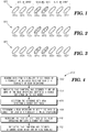
- a set of bits 100 includes a number of bits 102 ("array bits” or simply “bits" in an array (e.g., bits 102(a)-(f)) and one or more reference bits 104 (e.g., reference bits 104(a)-(b)) associated therewith.
- One reference bit 104(a) is designated “L” and nominally has a “low” signal (e.g., a low conductance value in an MRAM memory), and the other reference bit, 104(b), is designated “H” and nominally has a “high” signal (e.g., a high conductance value in an MRAM memory).
- Reference bits 104 are "associated with" bits 102 in the sense that they are used as references during a read operation performed on bits 102.
- FIG. 1 two reference bits 104 are illustrated.
- the present invention is not so limited, and may be implemented in memories utilizing any other number of reference bits. There may be, for example, 16 to 32 array bits per reference pair.
- the systems and methods described herein may be used in connection with an MRAM or any memory device that employs a midpoint generation scheme for reference bits.
- reference bit 104(b) - which would typically have a 'high” signal - might be toggled to a "low' signal state.
- bit 104(a) might be toggled from its normal "low” signal state to a "high” signal state.
- the average signal of reference bits 104 is ( L + H )/2.
- the average signal of reference bits 104 is reduced to ( L + H )/2.
- one or more low bits 102 may be incorrectly read as "high.”
- half of the read bits will be misread.
- the average signal of reference bits 104 is abnormally high - i.e., ( H + H )/2 . This will result in one or more high bits 102 being incorrectly read as "low.”
- the presence of even one disturbed reference bit 104 can lead to multiple read errors with respect to any bits 102 associated with the disturbed reference bit 104.
- toggle operation may comprise reading the bit states followed by writing the opposite state.
- One exemplary embodiment includes 1) use of double bit error detection ECC to identify when an accessed word has reached two fails, 2) use of multiple reads from different ECC words to guarantee no tampering has occurred, 3) alternately, use double forced writes to multiple ECC words for better sensitivity, 4) target the number of multiple ECC words to achieve a minimum detection rate, 5) use of a reference bit programming sequence upon detection of tampering, and 6) use of a write verify sequence to provide robust behavior under operation with cladded line reversal.
- the exemplary embodiments are used to identify tampering in secure applications, and supports recovery and continued use. Reading from multiple ECC words increases the probability of detecting tampering.
- FIGS. 4 and 5 are flow charts that illustrate exemplary embodiments of the error detection scheme disclosed herein.
- the various tasks performed in connection with processes 400 and 500 may be performed by software, hardware, firmware, or any combination thereof.
- the following description of processes 400 and 500 may refer to elements mentioned above in connection with FIG. 1-3 .
- portions of processes 400 and 500 may be performed by different elements of the described system, e.g., a processor or detection module.
- processes 400 and 500 may include any number of additional or alternative tasks, the tasks shown in FIGS. 4 and 5 need not be performed in the illustrated order, and processes 400 and 500 may be incorporated into a more comprehensive procedure or process having additional functionality not described in detail herein.
- one or more of the tasks shown in FIGS. 4 and 5 could be omitted from an embodiment of the processes 400 and 500 as long as the intended overall functionality remains intact.
- FIG. 4 is a flowchart depicting a method for detecting reference bit errors in accordance with one embodiment. These steps may be performed by a module within the memory or external to the memory, and may be implemented via hardware, software, firmware, or a combination thereof.
- ECC Error Correction Code
- SEC single-bit error correcting
- SECDED single-bit error correcting/double error detection
- the output of the ECC will typically include certain information related to the state of the data bit or bits that are read, e.g., a count of the number of errors as well as the locations (i.e., the physical locations) of the errors.
- the location of the corresponding reference bits(s) 104 will also be known.
- an indication is made that tampering has occurred if one or more of the read operations identifies a double bit error in the ECC words, and in step 406, the reference bits are reset upon detecting a double bit error.
- a read operation is performed to verify the data is correct for each of a plurality of write operations (step 408), and the data is rewritten at least once if the read operation indicates a double bit error (step 410).
- a further indication is made that tampering has occurred if errors occur after two or more rewrites (step 412).
- FIG. 5 is a flowchart depicting an alternate embodiment in which it is assumed that two or more bits per reference pair can be read in a single operation.
- the ECC words are toggled twice 502, and read 504. If a reading of the ECC words indicates a double bit error, an indication 506 is made that tampering has occurred, and the reference bits are reset 508 upon detecting of the double bit error.
- the detection and/or repair of reference bits is performed during regular memory operations, thus allowing for a transparent process and undisturbed operation of the memory.
- ECC detection step 402 may be performed during any convenient read operation.
- steps of toggling a reference bit (step 506) may be performed during any convenient write operation. In this process, the references are checked and repaired substantially continuously. This helps prevent disturbed reference bits from impacting read reliability.
- a log used to store the step in the flow and/or impacted addresses can be implemented using volatile or non-volatile elements. Use of non-volatile elements would prevent a power down event from interrupting the detection and correction sequence, but is not necessary for most applications. If non-volatile elements are used that require association with reference pairs, the bits associated with the log may be included in the ECC and reference detection scheme used.
- an exemplary semiconductor memory 600 includes a set of array bits 102 associated with a set of reference bits 104.
- a detection module 602 is configured to perform one or more ECC error detection steps to detect the presence of errors with array bits 102 and toggle one of the reference bits 104 from one state to a second state if the error count associated with the ECC error detection step is greater than the predetermined threshold, as described above.
- the detection module 602 may be implemented or realized with a general purpose processor, a content addressable memory, a digital signal processor, an application specific integrated circuit, a field programmable gate array, any suitable programmable logic device, discrete gate or transistor logic, discrete hardware components, or any combination designed to perform the functions described herein.
- a processor device may be realized as a microprocessor, a controller, a microcontroller, or a state machine.
- a processor device may be implemented as a combination of computing devices, e.g., a combination of a digital signal processor and a microprocessor, a plurality of microprocessors, one or more microprocessors in conjunction with a digital signal processor core, or any other such configuration.
Landscapes
- Engineering & Computer Science (AREA)
- Theoretical Computer Science (AREA)
- Physics & Mathematics (AREA)
- Quality & Reliability (AREA)
- General Engineering & Computer Science (AREA)
- General Physics & Mathematics (AREA)
- Probability & Statistics with Applications (AREA)
- Techniques For Improving Reliability Of Storages (AREA)
- For Increasing The Reliability Of Semiconductor Memories (AREA)
- Mram Or Spin Memory Techniques (AREA)
Claims (10)
- Procédé comprenant :le basculement (502) de bits de données (100) associés à un mot de code de correction d'erreur (ECC) d'un dispositif de mémoire (600) deux fois ;la lecture (504) des bits de données associés au mot ECC à partir du dispositif de mémoire ;la détection d'une double erreur sur les bits associée aux bits de données du mot ECC ; etla détermination (506) que le dispositif de mémoire a été altéré d'après la détection de la double erreur sur les bits associée aux bits de données associés au mot ECC.
- Procédé selon la revendication 1, dans lequel les bits de données associés au mot ECC comportent une pluralité de bits de référence (104).
- Procédé selon la revendication 2, comprenant en outre la réinitialisation de la pluralité de bits de référence (104) lors de la détection de la double erreur sur les bits.
- Procédé selon la revendication 1, comprenant en outre :la réalisation (408) d'une opération de lecture pour vérifier si des données stockées dans les bits de données sont correctes pour au moins une opération d'écriture ;la détermination qu'une première double erreur sur les bits supplémentaire s'est produite pour l'opération de lecture ;la réécriture (410) des données au moins une fois lorsque la première double erreur sur les bits supplémentaire s'est produite ;la détermination qu'une seconde double erreur sur les bits supplémentaire s'est produite après réécriture des données ; etl'indication (412) qu'une altération s'est produite lorsque des erreurs se produisent après réécriture des données.
- Dispositif de mémoire (600) comprenant :au moins une matrice, l'au moins une matrice ayant une pluralité de mots de code de correction d'erreur (ECC), des mots ECC individuels de la pluralité de mots ECC comportant des bits de données (100) respectifs et des bits de référence (104) respectifs ; et, le dispositif de mémoire comprenant des moyens réalisant toutes les étapes du procédé selon la revendication 1.
- Dispositif de mémoire (600) selon la revendication 5, dans lequel le dispositif de mémoire est en outre configuré pour basculer les bits de données respectifs et les bits de référence respectifs associés au mot ECC deux fois avant la lecture des bits de données respectifs et des bits de référence respectifs associés au mot ECC.
- Dispositif de mémoire (600) selon la revendication 5, dans lequel le dispositif de mémoire est en outre configuré pour réinitialiser les bits de référence respectifs associés à l'au moins un mot ECC lors de la détection que la double erreur sur les bits s'est produite.
- Dispositif de mémoire (600) selon la revendication 5, dans lequel le dispositif de mémoire est en outre configuré pour :indiquer qu'une altération s'est produite sur au moins un circuit associé au dispositif de mémoire.
- Dispositif de mémoire (600) selon la revendication 5, dans lequel le Dispositif de mémoire est en outre configuré pour réinitialiser les bits de référence respectifs lors de l'occurrence de la double erreur sur les bits.
- Procédé selon la revendication 1, dans lequel la détermination que le dispositif de mémoire (600) a été altéré comporte la détermination qu'une perturbation s'est produite, qu'une opération d'écriture a été dégradée par une exposition à un champ externe, ou les deux.
Applications Claiming Priority (2)
| Application Number | Priority Date | Filing Date | Title |
|---|---|---|---|
| US201161491761P | 2011-05-31 | 2011-05-31 | |
| PCT/US2012/040196 WO2012166910A1 (fr) | 2011-05-31 | 2012-05-31 | Détection de perturbation de champ de mram et rétablissement |
Publications (3)
| Publication Number | Publication Date |
|---|---|
| EP2715541A1 EP2715541A1 (fr) | 2014-04-09 |
| EP2715541A4 EP2715541A4 (fr) | 2014-11-26 |
| EP2715541B1 true EP2715541B1 (fr) | 2017-12-20 |
Family
ID=47259850
Family Applications (1)
| Application Number | Title | Priority Date | Filing Date |
|---|---|---|---|
| EP12792839.8A Active EP2715541B1 (fr) | 2011-05-31 | 2012-05-31 | Détection de perturbation de champ de mram et rétablissement |
Country Status (5)
| Country | Link |
|---|---|
| US (1) | US8984379B2 (fr) |
| EP (1) | EP2715541B1 (fr) |
| KR (1) | KR101983651B1 (fr) |
| CN (1) | CN103703447B (fr) |
| WO (1) | WO2012166910A1 (fr) |
Families Citing this family (9)
| Publication number | Priority date | Publication date | Assignee | Title |
|---|---|---|---|---|
| WO2014124271A1 (fr) * | 2013-02-08 | 2014-08-14 | Everspin Technologies, Inc. | Détection de tentatives d'altération et réaction à ces tentatives dans un dispositif mémoire |
| US9218509B2 (en) | 2013-02-08 | 2015-12-22 | Everspin Technologies, Inc. | Response to tamper detection in a memory device |
| US10146601B2 (en) | 2013-06-12 | 2018-12-04 | Everspin Technologies, Inc. | Methods and devices for healing reset errors in a magnetic memory |
| US9558066B2 (en) * | 2014-09-26 | 2017-01-31 | Intel Corporation | Exchanging ECC metadata between memory and host system |
| US10449811B2 (en) | 2015-06-15 | 2019-10-22 | Infineon Technologies Ag | Tire monitoring system and method |
| WO2017058111A1 (fr) * | 2015-09-28 | 2017-04-06 | Agency For Science, Technology And Research | Procédé de détection d'erreur dans un dispositif de mémoire vive magnétique à champ électrique oscillant (tef-ram), et dispositif tef-ram |
| TWI670717B (zh) * | 2016-09-13 | 2019-09-01 | 東芝記憶體股份有限公司 | 記憶裝置及記憶體系統 |
| DE102017124313B4 (de) * | 2017-10-18 | 2021-03-18 | Infineon Technologies Ag | Speicheranordnung und verfahren zum verifizieren eines speicherzugriffs |
| US11621026B2 (en) | 2020-12-01 | 2023-04-04 | International Business Machines Corporation | Write driver with magnetic field compensation |
Family Cites Families (16)
| Publication number | Priority date | Publication date | Assignee | Title |
|---|---|---|---|---|
| US5644583A (en) * | 1992-09-22 | 1997-07-01 | International Business Machines Corporation | Soft error correction technique and system for odd weight row error correction codes |
| US6331943B1 (en) * | 2000-08-28 | 2001-12-18 | Motorola, Inc. | MTJ MRAM series-parallel architecture |
| ATE441928T1 (de) | 2003-01-14 | 2009-09-15 | Nxp Bv | Manipulationsbeständige kapselung und ansatz mit magnetischgesetzten daten |
| US7320100B2 (en) * | 2003-05-20 | 2008-01-15 | Cray Inc. | Apparatus and method for memory with bit swapping on the fly and testing |
| US7536612B2 (en) | 2003-08-29 | 2009-05-19 | International Business Machines Corporation | Field spike monitor for MRAM |
| CN100547676C (zh) | 2003-11-24 | 2009-10-07 | Nxp股份有限公司 | 防止对磁阻存储器元件错误编程的方法和器件 |
| JP2007513502A (ja) | 2003-11-24 | 2007-05-24 | コーニンクレッカ フィリップス エレクトロニクス エヌ ヴィ | 磁界センサを有するmramチップの不均一シールド |
| US7543211B2 (en) * | 2005-01-31 | 2009-06-02 | Everspin Technologies, Inc. | Toggle memory burst |
| WO2007046350A1 (fr) | 2005-10-18 | 2007-04-26 | Nec Corporation | Procede de fonctionnement d'une mram |
| US7747926B2 (en) | 2006-05-02 | 2010-06-29 | Everspin Technologies, Inc. | Methods and apparatus for a memory device with self-healing reference bits |
| US8495438B2 (en) * | 2007-12-28 | 2013-07-23 | Texas Instruments Incorporated | Technique for memory imprint reliability improvement |
| US8677221B2 (en) | 2008-01-02 | 2014-03-18 | Apple Inc. | Partial voltage read of memory |
| US8255758B2 (en) | 2008-01-21 | 2012-08-28 | Apple Inc. | Decoding of error correction code using partial bit inversion |
| US8296626B2 (en) | 2008-11-07 | 2012-10-23 | Spansion Llc | Error correction for flash memory |
| US8111544B2 (en) | 2009-02-23 | 2012-02-07 | Taiwan Semiconductor Manufacturing Company, Ltd. | Programming MRAM cells using probability write |
| KR101688051B1 (ko) * | 2010-11-08 | 2016-12-20 | 삼성전자 주식회사 | 에러 검출 코드를 이용한 데이터 처리 장치, 데이터 처리 방법, 데이터 스큐 보상 방법 및 데이터 처리 장치를 포함하는 반도체 장치 |
-
2012
- 2012-05-31 US US13/484,509 patent/US8984379B2/en active Active
- 2012-05-31 EP EP12792839.8A patent/EP2715541B1/fr active Active
- 2012-05-31 KR KR1020137034683A patent/KR101983651B1/ko active IP Right Grant
- 2012-05-31 WO PCT/US2012/040196 patent/WO2012166910A1/fr unknown
- 2012-05-31 CN CN201280034545.3A patent/CN103703447B/zh active Active
Non-Patent Citations (1)
| Title |
|---|
| None * |
Also Published As
| Publication number | Publication date |
|---|---|
| CN103703447B (zh) | 2017-02-08 |
| US20120311396A1 (en) | 2012-12-06 |
| EP2715541A1 (fr) | 2014-04-09 |
| EP2715541A4 (fr) | 2014-11-26 |
| US8984379B2 (en) | 2015-03-17 |
| KR20140051864A (ko) | 2014-05-02 |
| KR101983651B1 (ko) | 2019-05-29 |
| WO2012166910A1 (fr) | 2012-12-06 |
| CN103703447A (zh) | 2014-04-02 |
Similar Documents
| Publication | Publication Date | Title |
|---|---|---|
| EP2715541B1 (fr) | Détection de perturbation de champ de mram et rétablissement | |
| US10019312B2 (en) | Error monitoring of a memory device containing embedded error correction | |
| US10108509B2 (en) | Dynamic enabling of redundant memory cells during operating life | |
| US8504884B2 (en) | Threshold voltage techniques for detecting an imminent read failure in a memory array | |
| US10564866B2 (en) | Bank-level fault management in a memory system | |
| US9208027B2 (en) | Address error detection | |
| US20080040652A1 (en) | Memory Error Detection Device and Method for Detecting a Memory Error | |
| US7747926B2 (en) | Methods and apparatus for a memory device with self-healing reference bits | |
| US20110107160A1 (en) | Time-based techniques for detecting an imminent read failure in a memory array | |
| JPH03248251A (ja) | 情報処理装置 | |
| US10795763B2 (en) | Memory system and error correcting method thereof | |
| US9858145B2 (en) | Selective error coding | |
| JP5869649B2 (ja) | データ処理のための方法、機器、および装置 | |
| KR101512927B1 (ko) | 비휘발성 메모리의 페이지 관리 방법 및 장치 | |
| US20090199043A1 (en) | Error correction in an integrated circuit with an array of memory cells | |
| CN106067326B (zh) | 错误校正电路及包括其的半导体存储器件 | |
| US9104568B2 (en) | Detection of memory cells that are stuck in a physical state | |
| US20200250029A1 (en) | Dynamic redundancy for memory | |
| US9032273B2 (en) | Method, apparatus and device for data processing | |
| US9940204B2 (en) | Memory error recovery | |
| JP2012230730A (ja) | 半導体装置 |
Legal Events
| Date | Code | Title | Description |
|---|---|---|---|
| PUAI | Public reference made under article 153(3) epc to a published international application that has entered the european phase |
Free format text: ORIGINAL CODE: 0009012 |
|
| 17P | Request for examination filed |
Effective date: 20140102 |
|
| AK | Designated contracting states |
Kind code of ref document: A1 Designated state(s): AL AT BE BG CH CY CZ DE DK EE ES FI FR GB GR HR HU IE IS IT LI LT LU LV MC MK MT NL NO PL PT RO RS SE SI SK SM TR |
|
| DAX | Request for extension of the european patent (deleted) | ||
| REG | Reference to a national code |
Ref country code: DE Ref legal event code: R079 Ref document number: 602012041160 Country of ref document: DE Free format text: PREVIOUS MAIN CLASS: G06F0011000000 Ipc: G06F0011100000 |
|
| A4 | Supplementary search report drawn up and despatched |
Effective date: 20141029 |
|
| RIC1 | Information provided on ipc code assigned before grant |
Ipc: H03M 13/11 20060101ALI20141023BHEP Ipc: G06F 11/10 20060101AFI20141023BHEP Ipc: G11C 29/44 20060101ALI20141023BHEP |
|
| GRAP | Despatch of communication of intention to grant a patent |
Free format text: ORIGINAL CODE: EPIDOSNIGR1 |
|
| INTG | Intention to grant announced |
Effective date: 20170706 |
|
| GRAS | Grant fee paid |
Free format text: ORIGINAL CODE: EPIDOSNIGR3 |
|
| GRAJ | Information related to disapproval of communication of intention to grant by the applicant or resumption of examination proceedings by the epo deleted |
Free format text: ORIGINAL CODE: EPIDOSDIGR1 |
|
| GRAL | Information related to payment of fee for publishing/printing deleted |
Free format text: ORIGINAL CODE: EPIDOSDIGR3 |
|
| GRAR | Information related to intention to grant a patent recorded |
Free format text: ORIGINAL CODE: EPIDOSNIGR71 |
|
| GRAA | (expected) grant |
Free format text: ORIGINAL CODE: 0009210 |
|
| INTC | Intention to grant announced (deleted) | ||
| INTG | Intention to grant announced |
Effective date: 20171108 |
|
| AK | Designated contracting states |
Kind code of ref document: B1 Designated state(s): AL AT BE BG CH CY CZ DE DK EE ES FI FR GB GR HR HU IE IS IT LI LT LU LV MC MK MT NL NO PL PT RO RS SE SI SK SM TR |
|
| REG | Reference to a national code |
Ref country code: GB Ref legal event code: FG4D |
|
| REG | Reference to a national code |
Ref country code: CH Ref legal event code: EP |
|
| REG | Reference to a national code |
Ref country code: IE Ref legal event code: FG4D |
|
| REG | Reference to a national code |
Ref country code: AT Ref legal event code: REF Ref document number: 956956 Country of ref document: AT Kind code of ref document: T Effective date: 20180115 |
|
| REG | Reference to a national code |
Ref country code: DE Ref legal event code: R096 Ref document number: 602012041160 Country of ref document: DE |
|
| REG | Reference to a national code |
Ref country code: NL Ref legal event code: MP Effective date: 20171220 |
|
| PG25 | Lapsed in a contracting state [announced via postgrant information from national office to epo] |
Ref country code: FI Free format text: LAPSE BECAUSE OF FAILURE TO SUBMIT A TRANSLATION OF THE DESCRIPTION OR TO PAY THE FEE WITHIN THE PRESCRIBED TIME-LIMIT Effective date: 20171220 Ref country code: SE Free format text: LAPSE BECAUSE OF FAILURE TO SUBMIT A TRANSLATION OF THE DESCRIPTION OR TO PAY THE FEE WITHIN THE PRESCRIBED TIME-LIMIT Effective date: 20171220 Ref country code: LT Free format text: LAPSE BECAUSE OF FAILURE TO SUBMIT A TRANSLATION OF THE DESCRIPTION OR TO PAY THE FEE WITHIN THE PRESCRIBED TIME-LIMIT Effective date: 20171220 Ref country code: NO Free format text: LAPSE BECAUSE OF FAILURE TO SUBMIT A TRANSLATION OF THE DESCRIPTION OR TO PAY THE FEE WITHIN THE PRESCRIBED TIME-LIMIT Effective date: 20180320 |
|
| REG | Reference to a national code |
Ref country code: LT Ref legal event code: MG4D |
|
| REG | Reference to a national code |
Ref country code: AT Ref legal event code: MK05 Ref document number: 956956 Country of ref document: AT Kind code of ref document: T Effective date: 20171220 |
|
| PG25 | Lapsed in a contracting state [announced via postgrant information from national office to epo] |
Ref country code: LV Free format text: LAPSE BECAUSE OF FAILURE TO SUBMIT A TRANSLATION OF THE DESCRIPTION OR TO PAY THE FEE WITHIN THE PRESCRIBED TIME-LIMIT Effective date: 20171220 Ref country code: GR Free format text: LAPSE BECAUSE OF FAILURE TO SUBMIT A TRANSLATION OF THE DESCRIPTION OR TO PAY THE FEE WITHIN THE PRESCRIBED TIME-LIMIT Effective date: 20180321 Ref country code: RS Free format text: LAPSE BECAUSE OF FAILURE TO SUBMIT A TRANSLATION OF THE DESCRIPTION OR TO PAY THE FEE WITHIN THE PRESCRIBED TIME-LIMIT Effective date: 20171220 Ref country code: HR Free format text: LAPSE BECAUSE OF FAILURE TO SUBMIT A TRANSLATION OF THE DESCRIPTION OR TO PAY THE FEE WITHIN THE PRESCRIBED TIME-LIMIT Effective date: 20171220 Ref country code: BG Free format text: LAPSE BECAUSE OF FAILURE TO SUBMIT A TRANSLATION OF THE DESCRIPTION OR TO PAY THE FEE WITHIN THE PRESCRIBED TIME-LIMIT Effective date: 20180320 |
|
| PG25 | Lapsed in a contracting state [announced via postgrant information from national office to epo] |
Ref country code: NL Free format text: LAPSE BECAUSE OF FAILURE TO SUBMIT A TRANSLATION OF THE DESCRIPTION OR TO PAY THE FEE WITHIN THE PRESCRIBED TIME-LIMIT Effective date: 20171220 |
|
| RAP2 | Party data changed (patent owner data changed or rights of a patent transferred) |
Owner name: EVERSPIN TECHNOLOGIES, INC. |
|
| PG25 | Lapsed in a contracting state [announced via postgrant information from national office to epo] |
Ref country code: CZ Free format text: LAPSE BECAUSE OF FAILURE TO SUBMIT A TRANSLATION OF THE DESCRIPTION OR TO PAY THE FEE WITHIN THE PRESCRIBED TIME-LIMIT Effective date: 20171220 Ref country code: ES Free format text: LAPSE BECAUSE OF FAILURE TO SUBMIT A TRANSLATION OF THE DESCRIPTION OR TO PAY THE FEE WITHIN THE PRESCRIBED TIME-LIMIT Effective date: 20171220 Ref country code: SK Free format text: LAPSE BECAUSE OF FAILURE TO SUBMIT A TRANSLATION OF THE DESCRIPTION OR TO PAY THE FEE WITHIN THE PRESCRIBED TIME-LIMIT Effective date: 20171220 Ref country code: EE Free format text: LAPSE BECAUSE OF FAILURE TO SUBMIT A TRANSLATION OF THE DESCRIPTION OR TO PAY THE FEE WITHIN THE PRESCRIBED TIME-LIMIT Effective date: 20171220 Ref country code: CY Free format text: LAPSE BECAUSE OF FAILURE TO SUBMIT A TRANSLATION OF THE DESCRIPTION OR TO PAY THE FEE WITHIN THE PRESCRIBED TIME-LIMIT Effective date: 20171220 |
|
| PG25 | Lapsed in a contracting state [announced via postgrant information from national office to epo] |
Ref country code: IT Free format text: LAPSE BECAUSE OF FAILURE TO SUBMIT A TRANSLATION OF THE DESCRIPTION OR TO PAY THE FEE WITHIN THE PRESCRIBED TIME-LIMIT Effective date: 20171220 Ref country code: RO Free format text: LAPSE BECAUSE OF FAILURE TO SUBMIT A TRANSLATION OF THE DESCRIPTION OR TO PAY THE FEE WITHIN THE PRESCRIBED TIME-LIMIT Effective date: 20171220 Ref country code: PL Free format text: LAPSE BECAUSE OF FAILURE TO SUBMIT A TRANSLATION OF THE DESCRIPTION OR TO PAY THE FEE WITHIN THE PRESCRIBED TIME-LIMIT Effective date: 20171220 Ref country code: AT Free format text: LAPSE BECAUSE OF FAILURE TO SUBMIT A TRANSLATION OF THE DESCRIPTION OR TO PAY THE FEE WITHIN THE PRESCRIBED TIME-LIMIT Effective date: 20171220 Ref country code: SM Free format text: LAPSE BECAUSE OF FAILURE TO SUBMIT A TRANSLATION OF THE DESCRIPTION OR TO PAY THE FEE WITHIN THE PRESCRIBED TIME-LIMIT Effective date: 20171220 Ref country code: IS Free format text: LAPSE BECAUSE OF FAILURE TO SUBMIT A TRANSLATION OF THE DESCRIPTION OR TO PAY THE FEE WITHIN THE PRESCRIBED TIME-LIMIT Effective date: 20180420 |
|
| REG | Reference to a national code |
Ref country code: DE Ref legal event code: R097 Ref document number: 602012041160 Country of ref document: DE |
|
| PLBE | No opposition filed within time limit |
Free format text: ORIGINAL CODE: 0009261 |
|
| STAA | Information on the status of an ep patent application or granted ep patent |
Free format text: STATUS: NO OPPOSITION FILED WITHIN TIME LIMIT |
|
| 26N | No opposition filed |
Effective date: 20180921 |
|
| PG25 | Lapsed in a contracting state [announced via postgrant information from national office to epo] |
Ref country code: DK Free format text: LAPSE BECAUSE OF FAILURE TO SUBMIT A TRANSLATION OF THE DESCRIPTION OR TO PAY THE FEE WITHIN THE PRESCRIBED TIME-LIMIT Effective date: 20171220 |
|
| REG | Reference to a national code |
Ref country code: CH Ref legal event code: PL |
|
| GBPC | Gb: european patent ceased through non-payment of renewal fee |
Effective date: 20180531 |
|
| REG | Reference to a national code |
Ref country code: BE Ref legal event code: MM Effective date: 20180531 |
|
| PG25 | Lapsed in a contracting state [announced via postgrant information from national office to epo] |
Ref country code: MC Free format text: LAPSE BECAUSE OF FAILURE TO SUBMIT A TRANSLATION OF THE DESCRIPTION OR TO PAY THE FEE WITHIN THE PRESCRIBED TIME-LIMIT Effective date: 20171220 |
|
| PG25 | Lapsed in a contracting state [announced via postgrant information from national office to epo] |
Ref country code: LI Free format text: LAPSE BECAUSE OF NON-PAYMENT OF DUE FEES Effective date: 20180531 Ref country code: SI Free format text: LAPSE BECAUSE OF FAILURE TO SUBMIT A TRANSLATION OF THE DESCRIPTION OR TO PAY THE FEE WITHIN THE PRESCRIBED TIME-LIMIT Effective date: 20171220 Ref country code: CH Free format text: LAPSE BECAUSE OF NON-PAYMENT OF DUE FEES Effective date: 20180531 |
|
| REG | Reference to a national code |
Ref country code: IE Ref legal event code: MM4A |
|
| PG25 | Lapsed in a contracting state [announced via postgrant information from national office to epo] |
Ref country code: LU Free format text: LAPSE BECAUSE OF NON-PAYMENT OF DUE FEES Effective date: 20180531 |
|
| PG25 | Lapsed in a contracting state [announced via postgrant information from national office to epo] |
Ref country code: FR Free format text: LAPSE BECAUSE OF NON-PAYMENT OF DUE FEES Effective date: 20180531 Ref country code: GB Free format text: LAPSE BECAUSE OF NON-PAYMENT OF DUE FEES Effective date: 20180531 Ref country code: IE Free format text: LAPSE BECAUSE OF NON-PAYMENT OF DUE FEES Effective date: 20180531 |
|
| PG25 | Lapsed in a contracting state [announced via postgrant information from national office to epo] |
Ref country code: BE Free format text: LAPSE BECAUSE OF NON-PAYMENT OF DUE FEES Effective date: 20180531 |
|
| PG25 | Lapsed in a contracting state [announced via postgrant information from national office to epo] |
Ref country code: MT Free format text: LAPSE BECAUSE OF NON-PAYMENT OF DUE FEES Effective date: 20180531 |
|
| PG25 | Lapsed in a contracting state [announced via postgrant information from national office to epo] |
Ref country code: TR Free format text: LAPSE BECAUSE OF FAILURE TO SUBMIT A TRANSLATION OF THE DESCRIPTION OR TO PAY THE FEE WITHIN THE PRESCRIBED TIME-LIMIT Effective date: 20171220 |
|
| PG25 | Lapsed in a contracting state [announced via postgrant information from national office to epo] |
Ref country code: PT Free format text: LAPSE BECAUSE OF FAILURE TO SUBMIT A TRANSLATION OF THE DESCRIPTION OR TO PAY THE FEE WITHIN THE PRESCRIBED TIME-LIMIT Effective date: 20171220 Ref country code: HU Free format text: LAPSE BECAUSE OF FAILURE TO SUBMIT A TRANSLATION OF THE DESCRIPTION OR TO PAY THE FEE WITHIN THE PRESCRIBED TIME-LIMIT; INVALID AB INITIO Effective date: 20120531 |
|
| PG25 | Lapsed in a contracting state [announced via postgrant information from national office to epo] |
Ref country code: MK Free format text: LAPSE BECAUSE OF NON-PAYMENT OF DUE FEES Effective date: 20171220 |
|
| PG25 | Lapsed in a contracting state [announced via postgrant information from national office to epo] |
Ref country code: AL Free format text: LAPSE BECAUSE OF FAILURE TO SUBMIT A TRANSLATION OF THE DESCRIPTION OR TO PAY THE FEE WITHIN THE PRESCRIBED TIME-LIMIT Effective date: 20171220 |
|
| P01 | Opt-out of the competence of the unified patent court (upc) registered |
Effective date: 20230523 |
|
| PGFP | Annual fee paid to national office [announced via postgrant information from national office to epo] |
Ref country code: DE Payment date: 20230530 Year of fee payment: 12 |