EP2709259A2 - Voltage balancing circuit - Google Patents
Voltage balancing circuit Download PDFInfo
- Publication number
- EP2709259A2 EP2709259A2 EP13184838.4A EP13184838A EP2709259A2 EP 2709259 A2 EP2709259 A2 EP 2709259A2 EP 13184838 A EP13184838 A EP 13184838A EP 2709259 A2 EP2709259 A2 EP 2709259A2
- Authority
- EP
- European Patent Office
- Prior art keywords
- voltage
- node
- groups
- capacitors
- resistance
- Prior art date
- Legal status (The legal status is an assumption and is not a legal conclusion. Google has not performed a legal analysis and makes no representation as to the accuracy of the status listed.)
- Withdrawn
Links
Images


Classifications
-
- G—PHYSICS
- G05—CONTROLLING; REGULATING
- G05F—SYSTEMS FOR REGULATING ELECTRIC OR MAGNETIC VARIABLES
- G05F5/00—Systems for regulating electric variables by detecting deviations in the electric input to the system and thereby controlling a device within the system to obtain a regulated output
-
- H—ELECTRICITY
- H02—GENERATION; CONVERSION OR DISTRIBUTION OF ELECTRIC POWER
- H02M—APPARATUS FOR CONVERSION BETWEEN AC AND AC, BETWEEN AC AND DC, OR BETWEEN DC AND DC, AND FOR USE WITH MAINS OR SIMILAR POWER SUPPLY SYSTEMS; CONVERSION OF DC OR AC INPUT POWER INTO SURGE OUTPUT POWER; CONTROL OR REGULATION THEREOF
- H02M1/00—Details of apparatus for conversion
- H02M1/32—Means for protecting converters other than automatic disconnection
-
- H—ELECTRICITY
- H02—GENERATION; CONVERSION OR DISTRIBUTION OF ELECTRIC POWER
- H02M—APPARATUS FOR CONVERSION BETWEEN AC AND AC, BETWEEN AC AND DC, OR BETWEEN DC AND DC, AND FOR USE WITH MAINS OR SIMILAR POWER SUPPLY SYSTEMS; CONVERSION OF DC OR AC INPUT POWER INTO SURGE OUTPUT POWER; CONTROL OR REGULATION THEREOF
- H02M5/00—Conversion of ac power input into ac power output, e.g. for change of voltage, for change of frequency, for change of number of phases
- H02M5/40—Conversion of ac power input into ac power output, e.g. for change of voltage, for change of frequency, for change of number of phases with intermediate conversion into dc
- H02M5/42—Conversion of ac power input into ac power output, e.g. for change of voltage, for change of frequency, for change of number of phases with intermediate conversion into dc by static converters
- H02M5/44—Conversion of ac power input into ac power output, e.g. for change of voltage, for change of frequency, for change of number of phases with intermediate conversion into dc by static converters using discharge tubes or semiconductor devices to convert the intermediate dc into ac
- H02M5/453—Conversion of ac power input into ac power output, e.g. for change of voltage, for change of frequency, for change of number of phases with intermediate conversion into dc by static converters using discharge tubes or semiconductor devices to convert the intermediate dc into ac using devices of a triode or transistor type requiring continuous application of a control signal
- H02M5/458—Conversion of ac power input into ac power output, e.g. for change of voltage, for change of frequency, for change of number of phases with intermediate conversion into dc by static converters using discharge tubes or semiconductor devices to convert the intermediate dc into ac using devices of a triode or transistor type requiring continuous application of a control signal using semiconductor devices only
-
- H—ELECTRICITY
- H02—GENERATION; CONVERSION OR DISTRIBUTION OF ELECTRIC POWER
- H02M—APPARATUS FOR CONVERSION BETWEEN AC AND AC, BETWEEN AC AND DC, OR BETWEEN DC AND DC, AND FOR USE WITH MAINS OR SIMILAR POWER SUPPLY SYSTEMS; CONVERSION OF DC OR AC INPUT POWER INTO SURGE OUTPUT POWER; CONTROL OR REGULATION THEREOF
- H02M7/00—Conversion of ac power input into dc power output; Conversion of dc power input into ac power output
- H02M7/42—Conversion of dc power input into ac power output without possibility of reversal
- H02M7/44—Conversion of dc power input into ac power output without possibility of reversal by static converters
- H02M7/48—Conversion of dc power input into ac power output without possibility of reversal by static converters using discharge tubes with control electrode or semiconductor devices with control electrode
-
- H—ELECTRICITY
- H02—GENERATION; CONVERSION OR DISTRIBUTION OF ELECTRIC POWER
- H02J—CIRCUIT ARRANGEMENTS OR SYSTEMS FOR SUPPLYING OR DISTRIBUTING ELECTRIC POWER; SYSTEMS FOR STORING ELECTRIC ENERGY
- H02J7/00—Circuit arrangements for charging or depolarising batteries or for supplying loads from batteries
- H02J7/0013—Circuit arrangements for charging or depolarising batteries or for supplying loads from batteries acting upon several batteries simultaneously or sequentially
- H02J7/0014—Circuits for equalisation of charge between batteries
-
- H—ELECTRICITY
- H02—GENERATION; CONVERSION OR DISTRIBUTION OF ELECTRIC POWER
- H02J—CIRCUIT ARRANGEMENTS OR SYSTEMS FOR SUPPLYING OR DISTRIBUTING ELECTRIC POWER; SYSTEMS FOR STORING ELECTRIC ENERGY
- H02J7/00—Circuit arrangements for charging or depolarising batteries or for supplying loads from batteries
- H02J7/34—Parallel operation in networks using both storage and other dc sources, e.g. providing buffering
- H02J7/345—Parallel operation in networks using both storage and other dc sources, e.g. providing buffering using capacitors as storage or buffering devices
Definitions
- Embodiments described herein relate to a voltage balancing circuit.
- load such as an electric motor is driven using a semiconductor switch after AC voltage has been converted to DC voltage by a rectifier and main circuit capacitors.
- the main circuit capacitors are connected in series to one another between main terminals since the circuit is required to have voltage proof against high DC voltage.
- leakage current flows through the main circuit capacitors. Since the leakage current flowing through the main circuit capacitors varies according to individual difference or temperature, voltage sharing of a plurality of main circuit capacitors changes with lapse of time, with the result of possibility that shared voltage would exceed a breakdown voltage of the main circuit capacitors.
- balancing resistances are generally connected between terminals of the main circuit capacitors. Since current constantly flows into the balancing resistances, mere supply of AC voltage to the device always results in a large amount of power loss. In view of this problem, it is desirable to change the number of series-connected smoothing main circuit capacitors after rectification according to AC voltage to be supplied. In this case, the breakdown voltage can be rendered higher when the number of series-connected main circuit capacitors is 3 or above but not 2.
- transistor-complementary elements are connected to a midpoint of a composition of series-connected electrolytic capacitors and a midpoint of a composition of series-connected resistances is connected to a common base terminal of the transistor-complementary elements.
- a voltage balancing circuit includes n-number of groups of resistances series-connected between a high voltage side first reference node and a low voltage side (n+1)-th reference node, between first and second main terminals to which DC voltage is supplied, where n ⁇ 3. N-number of groups of main circuit capacitors are series-connected between the high voltage side first output node and the low voltage side (n+1)-th output node between the first and second main terminals supplying DC voltage.
- the voltage balancing circuit is characterized by (N-1)-number of voltage stabilization circuits are configured between k-th reference nodes of the n-number of groups of resistances and k-th output nodes of the n-number of groups of main circuit capacitors respectively where 2 ⁇ k ⁇ n.
- Each voltage stabilization circuit includes first and second transistors of first and second conductivity types opposed to each other, respectively and having commonly connected reference input terminals and commonly connected output terminals, the reference input terminals being connected to the k-th reference nodes of the n-number of groups of main circuit capacitors, the output terminals being connected to the k-th output nodes of the n-number of groups of main circuit capacitors.
- the k-th voltage stabilization circuit is configured in such a manner that the first transistor is connected via a first resistance to a (k-a)-th output node serving as the source node and the second transistor is connected via a second resistance further connected to a (k+b)-th output node serving as the destination node, where 2 ⁇ k ⁇ n, 1 ⁇ a ⁇ k-1 and 1 ⁇ b ⁇ n+1-k.
- a first embodiment will be described with reference to FIGS. 1 to 3D .
- An inverter device of AC input voltage 690 volt class is particularly exemplified in the first embodiment.
- condition, (n, k, a, b) will be described later.
- the inverter 1 includes terminals R, S and T to which a three-phase AC power source 2 is connected.
- a rectifier 3 is connected to the terminals R, S and T.
- Three-phase AC power supplied to the terminals R, S and T is further supplied to the rectifier 3, which then rectifies the input AC power.
- Output of the rectifier 3 is supplied to main power lines N1 and N2.
- the main power line N1 serves as a first main terminal and has a node serving as a first reference node and a first output node.
- the main power line N2 serves as a second main terminal and has a node serving as a (n+1)-th reference node and a (n+1)-th output node.
- Three main circuit capacitors C1, C2 and C3 are connected in series to one another between the first and second main power lines N1 and N2.
- the capacitors C1 to C3 smooth output rectified by the rectifier 3, supplying DC power between the main power lines N1 and N2.
- two main circuit capacitors C1 and C2 may be series-connected when a three-phase AC power supply of about 400 V is used as the AC input voltage.
- a higher power supply such as the three-phase AC power supply 2 of effective value of 690 V is used, three capacitors C1 to C3 are series-connected with the result that high breakdown voltage can easily be realized.
- Each capacitor is comprised of an aluminum electrolytic capacitor.
- the capacitors C1 to C3 incorporate respective internal resistances r1 to r3, through each of which leakage current flows.
- Terminal voltages V 1 to V 3 in a normal operation are determined according to a ratio of capacitance values of the capacitors C1 to C3. Accordingly, capacitors having the same electrostatic capacitance value and the same breakdown voltage are used when three or more groups of capacitors are series-connected.
- the DC power smoothed by the capacitors C1 to C3 is supplied to an inverter main circuit 4.
- the inverter main circuit 4 converts the supplied DC power to corresponding AC power based on control signals of a control circuit 5, supplying the AC power from terminals U, V and W.
- the terminals U, V and W are connected to an electric motor 6 serving as load.
- the inverter device 1 supplies three-phase AC power via the terminals U, V and W to the motor 6.
- the control circuit 5 is comprised of a microcomputer, for example.
- the resistances R1 to R3 have the same resistance value.
- the transistor Tr1 has a collector connected to the resistance R4 and an emitter connected to an emitter of the second transistor Tr2.
- the second transistor Tr2 has a collector connected to the resistance R5.
- the common emitter (serving as an output terminal) of the transistors Tr1 and Tr2 is connected to a common connection node N3 of the capacitors C1 and C2. Furthermore, the transistors Tr1 and Tr2 have respective bases connected to each other and further to a node N5, whereby the bases serve as reference input terminals.
- a resistance R8 is connected between the common connection node N5 of the resistance R1 and R2 and the common connection node N3 of the capacitors C1 and C2.
- the voltage stabilization circuit 73 of the third group includes a resistance R6 (serving as a first resistance), an NPN transistor Tr3 (serving as the first transistor), a PNP transistor Tr4 and a resistance R7 (serving as a second resistance).
- the transistor Tr3 has a collector connected to the resistance R6 and an emitter connected to an emitter of the transistor Tr4.
- the transistor Tr4 has a collector connected to the resistance R7.
- the common emitter (serving as an output terminal) of the transistors Tr3 and Tr4 is connected to a common connection node N4 of the capacitors C2 and C3. Furthermore, bases of the transistors Tr3 and Tr4 connected to each other and further to a node N6, thereby serving as a reference input terminal.
- a resistance R9 is connected between the common connection node N6 of the resistances R2 and R3 and the common connection node N4.
- Leakage current characteristics of the capacitors C1 to C3 vary according to individual differences and temperature conditions. The individual differences in the leakage current characteristics result in different values of leakage currents of the capacitors C1 to C3 from one another. Accordingly, terminal voltages of the capacitors C1 to C3 also differ from one another, resulting in voltage unbalance.
- the terminal voltage V 1 is higher or lower than the terminal voltages V 2 and V 3 of the capacitors C2 and C3.
- the resistance R5 is set at a resistance value of 400 [k ⁇ ] corresponding to an addition of resistance values of two groups of the resistances R1 to R3.
- the resistance R4 is set at a resistance value of 200 [k ⁇ ] corresponding to the resistance value of one group of three resistances R1 to R3.
- the resistance R4 is set at a resistance value of 50 [k ⁇ ] corresponding to the resistance value of one group of resistance.
- a ratio of the resistance value of the resistance R4 to the resistance value of the resistance R5 is presented as 1:2, and the ratio corresponds to a resistance value ratio of the resistances of each group.
- These resistance value ratios of the resistances R4 and R5 are set by design according to a compensation amount of leakage current. Accordingly, the resistance value ratios of the resistances may not be used particularly but another resistance value may be used.
- a balance among voltages applied to the respective capacitors C1 to C3 can be maintained in an effective state when the resistances R4 to R7 connected to the collectors or emitters of the transistors Tr1 to Tr4 are set at the resistance values correspondingly proportional to the resistance values of the corresponding groups of resistances.
- electric current is supplied through the emitter-collector path of the transistor Tr2 so that the voltage at the node N3 substantially corresponds with the voltage at the node N5, so that the voltage at the node N3 can be controlled so as to substantially correspond with the voltage at the node N5.
- the terminal voltage V 1 of the capacitor C1 becomes larger than the terminal voltages V 2 and V 3 of the respective capacitors C2 and C3.
- the voltage at the node N3 then drops below a normal value 2 ⁇ V 0 /3.
- the voltages at the nodes N5 and N6 become divided voltages (2 ⁇ V 0 /3 and V 0 /3) of the resistances R1 to R3 respectively. Accordingly, since the voltage at the node N5 becomes higher than the voltage at the node N3, the base current flows into the transistor Tr1, which is turned on. Current is supplied from the node N1 via the resistance R4 to the node N3.
- the resistance R4 is set at a resistance value correspondingly proportional to the resistance of one (that is, resistance R1) of three resistances R1 to R3. Furthermore, the resistance R5 is set at a resistance value correspondingly proportional to two (that is, resistances R2 and R3) of three resistances R1 to R3. More specifically, when the resistance R4 is set at 200 [k ⁇ ], the resistance R5 is set at 400 [k ⁇ ]. Accordingly, electric current is supplied to the collector-emitter path of the transistor Tr1 so that the voltage at the node N3 substantially corresponds with the voltage at the node N5.
- FIG. 2 is a graph showing characteristics of terminal voltages of the capacitors according to respective leakage currents.
- FIGS. 3A to 3D show characteristics of currents flowing into the resistances R4, R5, R6 and R7 according to the leakage currents respectively.
- the vertical axis of the graph of FIG. 2 represents an inter-terminal voltage of each capacitor and the horizontal axis represents leakage current assumed to be generated in the capacitor C1.
- FIGS. 2 and 3A to 3D show the results of simulation in the case where leakage currents flowing through the respective capacitors C2 and C3 are 0.
- FIG. 3B shows that current proportional to the leakage current I flows into the resistance R5.
- the voltage at the node N3 is raised by this action, approximating to the normal value 2 ⁇ V 0 /3.
- the leakage currents of the capacitors C2 and C3 are assumed to be zero in the example as shown in FIG. 2 , the terminal voltage V 1 of the capacitor C1 drops below the terminal voltages V 2 and V 3 of the other capacitors C2 and C3 when the leakage current I of the capacitor C1 is larger than those of the other capacitors C2 and C3, as shown in FIG. 2 .
- the voltage balance can be rendered as favorable as possible since the terminal voltages V 2 and V 3 of the capacitors C2 and C3 can be substantially equal to each other.
- the differences between the maximum values and the minimum values of the terminal voltages V 1 to V 3 of the capacitors C1 to C3 become smaller in the embodiment than in a second embodiment which will be described later. Accordingly, the voltage balance in the embodiment can be rendered more favorable than in the second embodiment.
- the first main power supply line N1 serves as a common source node of the voltage stabilization circuits 72 and 73
- the second main power supply line N2 serves as the common destination node of the voltage stabilization circuits 72 and 73.
- the voltage stabilization circuits 72 and 73 which are connected to the respective common connection nodes N3 and N4 control the voltages at the nodes N3 and N4 so that the voltages are approximated to the respective normal values, 2 ⁇ V 0 /3 and V 0 /3, respectively. Accordingly, the voltages of the common connection nodes N3 and N4 of all the main circuit capacitors C1 to C3 can be approximated to the divided voltage, whereby the voltage unbalance can be resolved as much as possible.
- the transistors Tr1 to Tr4 are each maintained in the OFF state. Accordingly, since the resistances R4 to R7 do not result in power loss, electrical power consumption can be reduced. Consequently, the differences among leakage currents among the capacitors C1 to C3 can be compensated.
- FIGS. 4 to 6D illustrate a second embodiment.
- the second embodiment differs from the first embodiment in that the destination node of the voltage stabilization circuit 72 has been changed to the third output node N4 and the source node of the voltage stabilization circuit 73 has been changed to the second output node N3.
- Identical or similar parts in the second embodiment are labeled by the same reference symbols as those in the first embodiment and the description of these parts will be eliminated. Only the difference between the first and second embodiments will be described.
- the second main power supply line N2 (the (n+1)-th output node) serves as the destination node and is connected via the resistance R5 to the emitter of the transistor Tr2 in the voltage stabilization circuit 72.
- the first main power supply line N1 (the first output node) serves as the source node and is connected via the resistance R6 to the collector of the transistor Tr3.
- a node N4 (a third output node) serves as a destination node and is connected via the resistance R5 to the collector of the transistor Tr2 in the voltage stabilization circuit 72.
- a node N3 (a second output node) serves as a source node and is connected via the resistance R6 to the collector of the transistor Tr3.
- FIGS. 5 and 6A to 6D show characteristics corresponding to FIGS. 2 and 3A to 3D respectively.
- the vertical axis in FIG. 5 designates an inter-terminal voltage V of each capacitor and the horizontal axis designates a leakage current I assumed to occur in the capacitor C1.
- FIGS. 5 and 6A to 6D show the results of simulation carried out under the condition where leakage current flowing into each of the capacitors C2 and C3 is zero.
- leakage current flowing through each of the capacitors C2 and C3 is assumed to be zero in the example shown in FIG. 5
- terminal voltages of the capacitors C1, C2 and C3 are rendered larger in the sequence of V 1 , V 2 and V 3 when the leakage current of the capacitor C1 is large as shown in FIG. 5 .
- the voltage balance between the capacitors C1 and C2 and the voltage balance between the C2 and C3 can be improved in the second embodiment.
- the voltage balance between the capacitors C1 and C3 in the first embodiment is better than that in the second embodiment.
- a rectified and smoothed voltage V 0 is applied between the first and second main power supply lines N1 and N2.
- the voltage V 0 is divided into three parts and a device having the divided voltage with voltage margin as a breakdown voltage can be used as each transistor (Tr1, Tr2 and Tr3).
- each one of the transistors Tr2 and Tr3 has a collector-emitter breakdown voltage obtained by providing one group of voltage of two resistances (two-thirds of voltage V 0 ) with voltage margin.
- voltage obtained by providing voltage of one resistance with voltage margin can be used as the breakdown voltage in the second embodiment.
- a device having breakdown voltage which is as low as possible can be used as each one of the capacitors C1 to C3. Consequently, the second embodiment can provide a circuit arrangement advantageous in the costs.
- the terminal voltages V2 and V3 of the respective capacitors C2 and C3 are substantially at the same voltage as shown in FIG. 2 .
- the terminal voltage V3 of the capacitor C3 is higher than the terminal voltage V2 of the capacitor C2 as shown in FIG. 5 . Accordingly, the electrical potential at the node N4 is easy to increase and the transistor Tr4 is turned on. The potential at the node N4 can be controlled so as to drop by turning on the transistor Tr4. Even when the inverter device is wire connected in the above-described manner, the second embodiment can achieve the same operation and advantageous effect as the first embodiment.
- FIGS. 7 to 8D illustrate a third embodiment.
- Identical or similar parts in the third embodiment are labeled by the same reference symbols as those in the first and second embodiments and the description of these parts will be eliminated. Only the difference between the first and second embodiments and the third embodiment will be described.
- the combination of (n, k, a, b) should not be limited to those described above and particularly, the combination of "a” and "b” should not be limited to those described above.
- an intermediate voltage of the DC voltage is sometimes obtained according to the type thereof to be used. Accordingly, the even-numbered (four, for example) capacitors C1 to C4 are series-connected, and divided voltages of the same number of capacitors C1 and C2 and of the same number of capacitors C3 and C4 between the high-voltage side first main power supply line N1 and the low-voltage side second main power supply line N2.
- even-numbered resistances R1 to R3 and R14 are series-connected between the first and second main power supply lines N1 and N2
- even-numbered capacitors C1 to C4 are series-connected between the first and second main power supply lines N1 and N2, as shown in FIG. 7 .
- Reference symbols r1 to r4 designate internal resistances of the capacitors C1 to C4 in FIG. 7 .
- the voltage stabilization circuits 72, 73 and 74 are provided in the embodiment as shown in FIG. 7 .
- the voltage stabilization circuit 72 includes the transistors Tr1 and Tr2.
- the voltage stabilization circuit 73 includes the transistors Tr3 and Tr4.
- the voltage stabilization circuit 74 includes the NPN transistor Tr5 and the PNP transistor Tr6 both of which are connected so as to have a common base and a common emitter.
- the resistance R4 connected to the collector of the transistor Tr1 is further connected to the first main power supply line N1 (the first output node) as a source node.
- the resistance R6 connected to the collector of the transistor Tr3 is also connected to the first main power supply line N1 as a source node.
- a resistance R10 connected to the transistor Tr5 is also connected to the first main power supply line N1 as a source node.
- the resistance R5 connected to the collector of the transistor Tr2 is further connected to the second main power supply line N2 (a fifth output node) as a destination node.
- the resistance R7 connected to the collector of the transistor Tr4 is also connected the second main power supply line N2 as the destination node.
- a resistance R11 connected to the collector of the transistor Tr6 is further connected to the second main power supply line N2 as the destination node.
- a resistance R12 is connected between the common base and the common emitter of the transistor Tr5 and Tr6.
- the resistance R5 is set at a resistance value correspondingly proportional to a resistance value of three of four groups of resistances R1 to R3 and R14.
- the resistance R4 is set at a resistance value correspondingly proportional to one group of resistance value. In other words, a ratio of the resistance value of the resistance R4 to the resistance value of the resistance R5 is set to 1:3.
- the resistance R6 has a resistance value set so as to be correspondingly proportional to a resistance value of two of the four groups of resistances R1 to R3 and R14.
- the resistance R10 has a resistance value set so as to be correspondingly proportional to a resistance value of three of the four groups of resistances R1 to R3 and R14.
- the resistance R11 also has a resistance value set so as to be correspondingly proportional to the resistance value of one of the four groups of resistances. More specifically, the resistance values of the resistances R10 and R11 are set in ratio of 3:1.
- FIGS. 8A, 8B, 8C and 8D show the results of simulation in the case where an amount of leakage current of the capacitor C1 is larger, the case where an amount of leakage current of the capacitor C2 is larger, a case where an amount of leakage current of the capacitor C3 is larger and a case where an amount of leakage current of the capacitor C4 is larger, respectively.
- amounts of leakage current of the capacitors except for the target capacitor having a larger amount of leakage current are each assumed to be set at 0.
- amounts of leakage current of the capacitors C2 to C4 except for the target capacitor C1 are each assumed to be set at 0.
- the terminal voltage V 1 of the capacitor C1 is especially lower and the terminal voltages V2 to V4 of the respective capacitors C2 to C4 are substantially equivalent in the case of FIG. 8A .
- terminal voltages are presented in the relationship of V 2 ⁇ V 1 ⁇ V 3 ⁇ V 4 .
- FIG. 8B thus shows that the terminal voltages have high or low levels.
- terminal voltages are presented in the relationship of V 3 ⁇ V 1 ⁇ V 2 ⁇ V 4 .
- FIG. 8C also shows that the terminal voltages have high or low levels.
- terminal voltages are presented in the relationship of V 4 ⁇ V 1 ⁇ V 2 ⁇ V 3 .
- FIG. 8D further shows that the terminal voltages have high or low levels. More specifically, the terminal voltage of the capacitor having a larger amount of leakage current becomes lower while the terminal voltages of the other capacitors become higher.
- the transistor Tr2 When the potential at the node N3 is higher than the potential at the node N5, the transistor Tr2 is turned on, whereby the potential at the node N3 is controlled to become lower so that the potential at the node N3 substantially corresponds with the potential at the node N5.
- the transistor Tr1 when the potential at the node N3 is lower than the potential at the node N5, the transistor Tr1 is turned on, whereby the potential at the node N3 is controlled to become higher so that the potential at the node N3 substantially corresponds with the potential at the node N5.
- the transistor Tr4 when the potential at the node N4 is higher than the potential at the node N6, the transistor Tr4 is turned on, whereby the potential at the node N4 is controlled to become lower so that the potential at the node N4 substantially corresponds with the potential at the node N6.
- the transistor Tr3 when the potential at the node N4 is lower than the potential at the node N6, the transistor Tr3 is turned on, whereby the potential at the node N4 is controlled to become higher so that the potential at the node N4 substantially corresponds with the potential at the node N6.
- FIGS. 9 to 10D illustrate a fourth embodiment.
- the fourth embodiment differs from the first to third embodiments in that the source node and the destination node have been changed.
- FIGS. 10A, 10B, 10C and 10D show the results of simulation in the case where the capacitor C1 has a larger amount of leakage current, the case where the capacitor C2 has a larger amount of leakage current, the case where the capacitor C3 has a larger amount of leakage current and the case where the capacitor C4 has a larger amount of leakage current, respectively.
- amounts of leakage current of the capacitors except for the target capacitor having a larger amount of leakage current are each assumed to be set at 0.
- amounts of leakage current of the capacitors C2 to C4 except for the target capacitor C1 are each assumed to be set at 0.
- the terminal voltage V 1 of the capacitor C1 is particularly low and the terminal voltage V 2 of the capacitor C2 is higher than the terminal voltage V 1 .
- the terminal voltages V 3 and V 4 of the capacitors C3 and C4 are substantially equal to each other and are higher than the terminal voltage V 2 .
- terminal voltages are presented in the relationship of V 2 ⁇ V 1 ⁇ V 3 ⁇ V 4 .
- terminal voltages are presented in the relationship of V 3 ⁇ V 1 ⁇ V 2 ⁇ V 4 .
- terminal voltages are presented in the relationship of V 4 ⁇ V 3 ⁇ V 1 ⁇ V 2 .
- the terminal voltage of the capacitor having a larger amount of leakage current becomes lower while the terminal voltages of the other capacitors become higher in the same manner as in the foregoing embodiments. Consequently, the fourth embodiment can achieve the same operation and advantageous effect as the foregoing embodiments.
- FIGS. 11 to 12D illustrate a fifth embodiment.
- the fifth embodiment differs from the first to fourth embodiments in that the source node and the destination node have been changed.
- the voltage stabilization circuit 72 includes a source node of the resistance R4 which is connected to the collector of the transistor Tr1 and serves as the first main power supply line N1 (the first output node).
- the voltage stabilization circuit 72 also includes a destination node of the resistance R5 which is connected to the collector of the transistor Tr2 and serves as a node N7 (a fourth output node).
- the voltage stabilization circuit 73 includes a source node of the resistance R6 which is connected to the collector of the transistor Tr3 and serves as the node N3 (the second output node).
- the voltage stabilization circuit 73 also includes a destination node of the resistance R7 which is connected to the collector of the transistor Tr4 and serves as the node N7 (the fourth output node).
- the voltage stabilization circuit 74 includes a source node of the resistance R10 which is connected to the collector of the transistor Tr5 and serves as the node N3 (the second output node).
- the voltage stabilization circuit 74 also includes a destination node of the resistance R11 which is connected to the collector of the transistor Tr6 and serves as the second main power supply line N2 (a fifth output node).
- FIGS. 12A, 12B, 12C and 12D show the results of simulation in the case where the capacitor C1 has a larger amount of leakage current, the case where the capacitor C2 has a larger amount of leakage current, the case where the capacitor C3 has a larger amount of leakage current and the case where the capacitor C4 has a larger amount of leakage current, respectively.
- amounts of leakage current of the capacitors except for the target capacitor having a larger amount of leakage current are each assumed to be set at 0.
- amounts of leakage current of the capacitors C2 to C4 except for the target capacitor C1 are each assumed to be set at 0.
- the terminal voltage V 1 of the capacitor C1 is particularly low and the terminal voltages V3 and V 2 of the capacitors C3 and C2 are higher than the terminal voltage V 1 .
- the terminal voltage V 4 of the capacitor C4 is higher than the terminal voltages V 3 and V 2 .
- terminal voltages are presented in the relationship of V 2 ⁇ V 1 ⁇ V 3 ⁇ V 4
- terminal voltages are presented in the relationship of V 3 ⁇ V 2 ⁇ V 4 ⁇ V 1
- terminal voltages are presented in the relationship of V 4 ⁇ V 2 ⁇ V 3 ⁇ V 1 .
- the terminal voltage of the capacitor having a larger amount of leakage current becomes lower while the terminal voltages of the other capacitors become higher, in the same manner as in the foregoing embodiments. Consequently, the fifth embodiment can achieve the same operation and advantageous effect as the foregoing embodiments.
- FIGS. 13 to 14D illustrate a sixth embodiment.
- the sixth embodiment differs from the first to fifth embodiments in that the source node and the destination node have been changed.
- the voltage stabilization circuit 72 includes a source node of the resistance R4 which is connected to the collector of the transistor Tr1 and serves as the first main power supply line N1 (the first output node).
- the voltage stabilization circuit 72 also includes a destination node of the resistance R5 which is connected to the collector of the transistor Tr2 and serves as a node N4 (a third output node).
- the voltage stabilization circuit 73 includes a source node of the resistance R6 which is connected to the collector of the transistor Tr3 and serves as the node N3 (the second output node).
- the voltage stabilization circuit 73 also includes a destination node of the resistance R7 which is connected to the collector of the transistor Tr4 and serves as the node N7 (the fourth output node).
- the voltage stabilization circuit 74 includes a source node of the resistance R10 which is connected to the collector of the transistor Tr5 and serves as the node N4 (the third output node).
- the voltage stabilization circuit 74 also includes a destination node of the resistance R11 which is connected to the collector of the transistor Tr6 and serves as the second main power supply line N2 (a fifth output node).
- FIGS. 14A, 14B, 14C and 14D show the results of simulation in the case where the capacitor C1 has a larger amount of leakage current, the case where the capacitor C2 has a larger amount of leakage current, the case where the capacitor C3 has a larger amount of leakage current and the case where the capacitor C4 has a larger amount of leakage current, respectively.
- amounts of leakage current of the capacitors except for the target capacitor having a larger amount of leakage current are each assumed to be set at 0.
- amounts of leakage current of the capacitors C2 to C4 except for the target capacitor C1 are each assumed to be set at 0.
- the terminal voltage V 1 of the capacitor C1 is particularly low and the terminal voltages V 2 , V 3 and V 4 of the capacitors C2, C3 and C4 are sequentially higher than the terminal voltage V 1 in this order.
- terminal voltages are presented in the relationship of V 2 ⁇ V 1 ⁇ V 3 ⁇ V 4 .
- terminal voltages are presented in the relationship of V 3 ⁇ V 2 ⁇ V 4 ⁇ V 1 .
- terminal voltages are presented in the relationship of V 4 ⁇ V 3 ⁇ V 2 ⁇ V 1 .
- the terminal voltage of the capacitor having a larger amount of leakage current becomes lower while the terminal voltages of the other capacitors become higher, in the same manner as in the foregoing embodiments. Consequently, the sixth embodiment can achieve the same operation and advantageous effect as the foregoing embodiments.
- the circuit configuration of the third embodiment indicates a highest performance of the third to sixth embodiments.
- the fourth and fifth embodiments indicate second and third highest performances respectively and the sixth embodiment ( FIG. 13 ) indicates a lowest performance of the four embodiments.
- the collector-emitter breakdown voltage of each one of the transistors Tr1 to Tr6 composing the voltage stabilization circuits 72, 73 and 74 is set so as to correspond to the voltage of the number of groups between the source and destination nodes. Accordingly, the transistor Tr2 is set at a collector-emitter breakdown voltage corresponding to three groups of DC voltage applied to four groups of resistances R1 to R3 and R14 in the third embodiment ( FIG. 7 ). Similarly, each of the transistors Tr3 and Tr4 is set at a collector-emitter breakdown voltage corresponding to two groups of DC voltage applied to four groups of resistances R1 to R3 and R14. Furthermore, the transistor Tr5 is set at a collector-emitter breakdown voltage corresponding to three groups of DC voltage applied to four groups of resistances R1 to R3 and R14.
- each of the transistors Tr3 and Tr4 is set at a collector-emitter breakdown voltage corresponding to two groups of DC voltage applied to four groups of resistances R1 to R3 and R14.
- each of the transistors Tr2 and Tr5 is set at a collector-emitter breakdown voltage corresponding to two groups of DC voltage applied to four groups of resistances R1 to R3 and R14.
- each one of the transistors Tr1 to Tr6 merely requires a collector-emitter breakdown voltage corresponding to one group of DC voltage applied to the resistances R1 to R3 and R14.
- the sixth embodiment presents a most advantageous circuit configuration since the circuit can be composed of transistors each of which has a lower collector-emitter breakdown voltage.
- the circuit of the sixth embodiment can be composed of transistors each of which has a lowest collector-emitter breakdown voltage of the third to sixth embodiments.
- the collector-emitter breakdown voltage becomes higher in the sequence of the circuits of the fifth ( FIG. 11 ), fourth ( FIG. 9 ) and third ( FIG. 7 ) embodiments.
- Using transistors each of which has a lower collector-emitter breakdown voltage is advantageous in costs.
- the circuit configuration of the sixth embodiment ( FIG. 13 ) is most advantageous of those of the third to sixth embodiments. Although any one of the circuit configurations of the third to sixth embodiments may be used, it is desirable to configure a circuit by trade-off between voltage balance performance and the collector-emitter breakdown voltages of transistors.
- the foregoing embodiments should not be restrictive but may be modified or expanded as follows.
- the combination of the condition (n, k, a, b) should not be limited to those employed in the foregoing embodiments.
- a voltage stabilization circuit configured on the basis of a combination of the condition (n, k, a, b) as shown in FIG. 15 .
- a case where n ⁇ 5 may be applicable.
- the resistance R8 is connected between the common base and the common emitter between the transistors Tr1 and Tr2.
- the resistance R9 is connected between the common base and the common emitter between the transistors Tr3 and Tr4.
- the resistance R12 is connected between the common base and the common emitter between the transistors Tr5 and Tr6.
- the resistances R8, R9 and R12 may be provided as needed.
- the resistances connected to the collectors of the transistors Tr1 to Tr6 are set at the resistance values correspondingly proportional to the numbers of groups of the resistances R1 to R3 and R14.
- the resistances may not be strictly set at the respective exemplified resistance values but may be changed to appropriate values.
- the voltage between the main terminals is divided by n-number of groups of resistances and also by n-number of groups of main circuit capacitors. However, since each main circuit capacitor causes leakage current, the divided voltage fluctuates.
- An (n-1)-number of voltage stabilization circuits each include the first and second transistors.
- the (k-a)-th output node serving as the source node is connected via the first resistance correspondingly proportional to, for example, a-number of groups and the first transistor to the output terminals of the first and second transistors.
- the (k+b)-th output node serving as the destination node is connected to the output terminals of the first and second transistors via the second resistance correspondingly proportional to, for example, b-number of resistances and via the second transistor. Accordingly, when the voltage at the k-th reference node of n-number of resistances is lower than the voltage at the k-th output node of n-number of main circuit capacitors, electric current is supplied from the output terminal via the second transistor to the (k+b)-th output node, whereupon the voltage at the k-th output node of the main circuit capacitor connected to the output terminal can be controlled to be reduced.
- the k-th (2 ⁇ k ⁇ n) voltage stabilization circuit can stabilize the voltage at the k-th output node into the normal voltage, the voltages at the common connection nodes of all the main circuit capacitors can be stabilized so as to be approximated to the normal values. Consequently, unbalance among the terminal voltages of all the main circuit capacitors can be resolved as much as possible as compared with the conventional technique in which voltage balance is not carried out among a plurality of pairs of main circuit capacitors although voltage balance is carried out between a pair of adjacent main circuit capacitors.
Abstract
Description
- Embodiments described herein relate to a voltage balancing circuit.
- For example, in an electrical circuit such as an inverter, load such as an electric motor is driven using a semiconductor switch after AC voltage has been converted to DC voltage by a rectifier and main circuit capacitors. The main circuit capacitors are connected in series to one another between main terminals since the circuit is required to have voltage proof against high DC voltage.
- In the above-described inverter, leakage current flows through the main circuit capacitors. Since the leakage current flowing through the main circuit capacitors varies according to individual difference or temperature, voltage sharing of a plurality of main circuit capacitors changes with lapse of time, with the result of possibility that shared voltage would exceed a breakdown voltage of the main circuit capacitors. In view of the possibility, balancing resistances are generally connected between terminals of the main circuit capacitors. Since current constantly flows into the balancing resistances, mere supply of AC voltage to the device always results in a large amount of power loss. In view of this problem, it is desirable to change the number of series-connected smoothing main circuit capacitors after rectification according to AC voltage to be supplied. In this case, the breakdown voltage can be rendered higher when the number of series-connected main circuit capacitors is 3 or above but not 2.
- Techniques for obtaining voltage balance have conventionally been proposed. In one proposed technique, transistor-complementary elements are connected to a midpoint of a composition of series-connected electrolytic capacitors and a midpoint of a composition of series-connected resistances is connected to a common base terminal of the transistor-complementary elements.
- However, consider now a case where four or more even-numbered compositions of series-connected electrolytic capacitors are used and the adjacent compositions connected in series to each other constitute one pair. In this case, when voltage balance is to be improved between the compositions of each pair, it would be difficult to improve voltage balance between the pairs of compositions.
- Several embodiments will be described with reference to the accompanying drawings, in which:
-
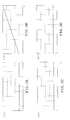
FIG. 1 is a diagram showing an electrical arrangement of an inverter device according to a first embodiment; -
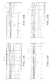
FIG. 2 is a graph showing terminal voltage characteristics of main circuit capacitors according to leakage current in the first embodiment; -
FIGS. 3A to 3D are graphs showing characteristics of current flowing into respective resistances according to leakage current in the first embodiment; -
FIG. 4 is a view similar toFIG. 1 , showing an electrical arrangement of the inverter device according to a second embodiment; -
FIG. 5 is a graph similar toFIG. 2 , showing the terminal voltage characteristics in the second embodiment; -
FIGS. 6A to 6D are graphs similar toFIGS. 3A to 3D , showing the current characteristics in the second embodiment; -
FIG. 7 is a view similar toFIG. 1 , showing an electrical arrangement of the inverter device according to a third embodiment; -
FIGS. 8A to 8D are graphs similar toFIG. 2 , showing the terminal voltage characteristics in the third embodiment; -
FIG. 9 is a view similar toFIG. 1 , showing the inverter device according to a fourth embodiment; -
FIGS. 10A to 10D are graphs similar toFIG. 2 , showing the terminal voltage characteristics in the fourth embodiment; -
FIG. 11 is a view similar toFIG. 1 , showing the inverter device according to a fifth embodiment; -
FIGS. 12A to 12D are graphs similar toFIG. 2 , showing the terminal voltage characteristics in the fifth embodiment; -
FIG. 13 is a view similar toFIG. 1 , showing the inverter device according to a sixth embodiment; -
FIGS. 14A to 14D are graphs similar toFIG. 2 , showing the terminal voltage characteristics in the sixth embodiment; and -
FIG. 15 shows combinations of voltage stabilization circuits regarding all the embodiments. - In general, according to one embodiment, a voltage balancing circuit includes n-number of groups of resistances series-connected between a high voltage side first reference node and a low voltage side (n+1)-th reference node, between first and second main terminals to which DC voltage is supplied, where n≥3. N-number of groups of main circuit capacitors are series-connected between the high voltage side first output node and the low voltage side (n+1)-th output node between the first and second main terminals supplying DC voltage. The voltage balancing circuit is characterized by (N-1)-number of voltage stabilization circuits are configured between k-th reference nodes of the n-number of groups of resistances and k-th output nodes of the n-number of groups of main circuit capacitors respectively where 2≤k≤n. Each voltage stabilization circuit includes first and second transistors of first and second conductivity types opposed to each other, respectively and having commonly connected reference input terminals and commonly connected output terminals, the reference input terminals being connected to the k-th reference nodes of the n-number of groups of main circuit capacitors, the output terminals being connected to the k-th output nodes of the n-number of groups of main circuit capacitors. When voltage of each reference input terminal is higher than voltage of each output terminal, power is supplied from a source node via the first transistor to the output terminal, and when the voltage of each reference input terminal is lower than the voltage of each output terminal, power is supplied from the output terminal via the second transistor to a destination node, whereby the voltage of the output terminal is stabilized so as to correspond with the voltage of the reference input terminal. The k-th voltage stabilization circuit is configured in such a manner that the first transistor is connected via a first resistance to a (k-a)-th output node serving as the source node and the second transistor is connected via a second resistance further connected to a (k+b)-th output node serving as the destination node, where 2≤k≤n, 1≤a≤k-1 and 1≤b≤n+1-k.
- Several embodiments will be described with reference to the accompanying drawings. Identical or similar parts will be labeled by the same or similar reference symbols throughout the embodiments.
- A first embodiment will be described with reference to
FIGS. 1 to 3D . An inverter device of AC input voltage 690 volt class is particularly exemplified in the first embodiment. The first embodiment is directed to a combination of voltage stabilization circuits configured to meet a condition, (n, k, a, b)=(3, 2, 1, 2) and (n, k, a, b)=(3, 3, 2, 1) respectively. The meaning of condition, (n, k, a, b) will be described later. - The
inverter 1 includes terminals R, S and T to which a three-phaseAC power source 2 is connected. Arectifier 3 is connected to the terminals R, S and T. Three-phase AC power supplied to the terminals R, S and T is further supplied to therectifier 3, which then rectifies the input AC power. Output of therectifier 3 is supplied to main power lines N1 and N2. - The main power line N1 serves as a first main terminal and has a node serving as a first reference node and a first output node. The main power line N2 serves as a second main terminal and has a node serving as a (n+1)-th reference node and a (n+1)-th output node. Three main circuit capacitors C1, C2 and C3 are connected in series to one another between the first and second main power lines N1 and N2. The capacitors C1 to C3 smooth output rectified by the
rectifier 3, supplying DC power between the main power lines N1 and N2. - For example, two main circuit capacitors C1 and C2 may be series-connected when a three-phase AC power supply of about 400 V is used as the AC input voltage. However, when a higher power supply such as the three-phase
AC power supply 2 of effective value of 690 V is used, three capacitors C1 to C3 are series-connected with the result that high breakdown voltage can easily be realized. - Three capacitors C1 to C3 are series-connected between the main power supply lines N1 and N2 in the embodiment. Each capacitor is comprised of an aluminum electrolytic capacitor. The capacitors C1 to C3 incorporate respective internal resistances r1 to r3, through each of which leakage current flows.
- Individual differences occur in characteristic values such as a leakage current characteristic, a temperature characteristic and the like in the capacitors C1 to C3. As a result, voltage tends to become unbalanced according to the individual differences. Terminal voltages V1 to V3 in a normal operation are determined according to a ratio of capacitance values of the capacitors C1 to C3. Accordingly, capacitors having the same electrostatic capacitance value and the same breakdown voltage are used when three or more groups of capacitors are series-connected. In the following description, a node N3 serving as a second output node (k=2) will refer to a common connection point between adjacent capacitors C1 and C2, and a node N4 serving as a third output node (k=3) will refer to a common connection point between adjacent capacitors C2 and C3.
- DC power smoothed by the capacitors C1 to C3 is supplied to an inverter
main circuit 4. The invertermain circuit 4 converts the supplied DC power to corresponding AC power based on control signals of acontrol circuit 5, supplying the AC power from terminals U, V and W. The terminals U, V and W are connected to anelectric motor 6 serving as load. Theinverter device 1 supplies three-phase AC power via the terminals U, V and W to themotor 6. Thecontrol circuit 5 is comprised of a microcomputer, for example. - Three groups (n=3) of reference voltage generating resistances R1 to R3 are series-connected between the main power supply lines N1 and N2. The resistances R1 to R3 have the same resistance value. In the following description, a node N5 (serving as a second reference node (k=2)) will refer to a common connection point between the adjacent resistances R1 and R2 and a node N6 (serving as a third reference node (k=3)) will refer to a common connection point between the resistances R2 and R3.
-
Voltage stabilization circuits voltage stabilization circuit 72 includes a resistance R4 (serving as a first resistance), an NPN transistor Tr1 (serving as a first transistor), a PNP transistor Tr2 (serving as a second transistor) and a resistance R5 (serving as a second resistance), all of which are connected in series to one another. The transistor Tr1 has a collector connected to the resistance R4 and an emitter connected to an emitter of the second transistor Tr2. - The second transistor Tr2 has a collector connected to the resistance R5.
- The common emitter (serving as an output terminal) of the transistors Tr1 and Tr2 is connected to a common connection node N3 of the capacitors C1 and C2. Furthermore, the transistors Tr1 and Tr2 have respective bases connected to each other and further to a node N5, whereby the bases serve as reference input terminals. A resistance R8 is connected between the common connection node N5 of the resistance R1 and R2 and the common connection node N3 of the capacitors C1 and C2.
- Furthermore, the
voltage stabilization circuit 73 of the third group (k=3) includes a resistance R6 (serving as a first resistance), an NPN transistor Tr3 (serving as the first transistor), a PNP transistor Tr4 and a resistance R7 (serving as a second resistance). The transistor Tr3 has a collector connected to the resistance R6 and an emitter connected to an emitter of the transistor Tr4. The transistor Tr4 has a collector connected to the resistance R7. - The common emitter (serving as an output terminal) of the transistors Tr3 and Tr4 is connected to a common connection node N4 of the capacitors C2 and C3. Furthermore, bases of the transistors Tr3 and Tr4 connected to each other and further to a node N6, thereby serving as a reference input terminal. A resistance R9 is connected between the common connection node N6 of the resistances R2 and R3 and the common connection node N4.
- The condition, (n, k, a, b) means that when n-number (n=3) of groups of reference voltage generation resistances R1 to R3 are connected, the k-th (k=2, 3) group of
voltage stabilization circuits - The operation of the above-described configuration will now be described. In the following description, a maximum value of AC power supply voltage (= 690×√2) will be defined as DC voltage V0 supplied to the inverter
main circuit 4. Leakage current characteristics of the capacitors C1 to C3 vary according to individual differences and temperature conditions. The individual differences in the leakage current characteristics result in different values of leakage currents of the capacitors C1 to C3 from one another. Accordingly, terminal voltages of the capacitors C1 to C3 also differ from one another, resulting in voltage unbalance. The following description of the operation is directed to the case where the leakage current of the capacitor C1 differs from the leakage currents of the capacitors C2 and C3 and accordingly, the terminal voltage V1 is higher or lower than the terminal voltages V2 and V3 of the capacitors C2 and C3. - When the capacitor C1 has a larger leakage current than the other capacitors C2 and C3, the terminal voltage V1 of the capacitor C1 drops below the terminal voltages V2 and V3 of the respective capacitors C2 and C3. Then, voltage at node N3 rises above a divided voltage (2×V0/3) and voltage at node N4 also rises above a divided voltage (V0/3).
- Voltages at nodes N5 and N6 are divided by the respective three groups of resistances R1 to R3. Accordingly, the voltages at nodes N5 and N6 are divided voltages (= 2 × V0/3, V0/3) correspond to each other. However, since the voltage at the node N5 is lower than the voltage at the node N3, the transistor Tr2 is turned on when a base current flows into the transistor Tr2. In this case, the resistance R5 is set at a resistance value correspondingly proportional to a resistance value obtained by adding resistance values of two (that is, resistances R2 and R3) of the three groups of resistances R1 to R3. The resistance R4 is set at a resistance value correspondingly proportional to a resistance value of one of three resistances R1 to R3.
- When each one of the reference voltage generating resistances R1 to R3 is set at 200 [kΩ] in the embodiment, the resistance R5 is set at a resistance value of 400 [kΩ] corresponding to an addition of resistance values of two groups of the resistances R1 to R3. The resistance R4 is set at a resistance value of 200 [kΩ] corresponding to the resistance value of one group of three resistances R1 to R3. Furthermore, as another example, when the resistance R5 is set at a resistance value of 100 [kΩ] corresponding to an addition of resistance values of two groups of the three resistances, the resistance R4 is set at a resistance value of 50 [kΩ] corresponding to the resistance value of one group of resistance. More specifically, a ratio of the resistance value of the resistance R4 to the resistance value of the resistance R5 is presented as 1:2, and the ratio corresponds to a resistance value ratio of the resistances of each group. These resistance value ratios of the resistances R4 and R5 are set by design according to a compensation amount of leakage current. Accordingly, the resistance value ratios of the resistances may not be used particularly but another resistance value may be used.
- Thus, a balance among voltages applied to the respective capacitors C1 to C3 can be maintained in an effective state when the resistances R4 to R7 connected to the collectors or emitters of the transistors Tr1 to Tr4 are set at the resistance values correspondingly proportional to the resistance values of the corresponding groups of resistances. In this case, electric current is supplied through the emitter-collector path of the transistor Tr2 so that the voltage at the node N3 substantially corresponds with the voltage at the node N5, so that the voltage at the node N3 can be controlled so as to substantially correspond with the voltage at the node N5.
- Conversely, when the capacitor C1 has a smaller leakage current than the other capacitors C2 and C3, the terminal voltage V1 of the capacitor C1 becomes larger than the terminal voltages V2 and V3 of the respective capacitors C2 and C3. The voltage at the node N3 then drops below a
normal value 2×V0/3. The voltages at the nodes N5 and N6 become divided voltages (2×V0/3 and V0/3) of the resistances R1 to R3 respectively. Accordingly, since the voltage at the node N5 becomes higher than the voltage at the node N3, the base current flows into the transistor Tr1, which is turned on. Current is supplied from the node N1 via the resistance R4 to the node N3. - In the above-described case, the resistance R4 is set at a resistance value correspondingly proportional to the resistance of one (that is, resistance R1) of three resistances R1 to R3. Furthermore, the resistance R5 is set at a resistance value correspondingly proportional to two (that is, resistances R2 and R3) of three resistances R1 to R3. More specifically, when the resistance R4 is set at 200 [kΩ], the resistance R5 is set at 400 [kΩ]. Accordingly, electric current is supplied to the collector-emitter path of the transistor Tr1 so that the voltage at the node N3 substantially corresponds with the voltage at the node N5. Even when any one of the leakage currents of the main circuit capacitors C1 to C3 differs, the
voltage stabilization circuits - The inventors simulated terminal voltages of the capacitors C1 to C3, leakage current I and characteristics of current flowing into the resistance R5 (during ON of the transistor Tr2) when leakage current of the capacitor C1 is larger than leakage currents of the other capacitors C2 and C3.
FIG. 2 is a graph showing characteristics of terminal voltages of the capacitors according to respective leakage currents.FIGS. 3A to 3D show characteristics of currents flowing into the resistances R4, R5, R6 and R7 according to the leakage currents respectively. The vertical axis of the graph ofFIG. 2 represents an inter-terminal voltage of each capacitor and the horizontal axis represents leakage current assumed to be generated in the capacitor C1.FIGS. 2 and3A to 3D show the results of simulation in the case where leakage currents flowing through the respective capacitors C2 and C3 are 0. -
FIG. 3B shows that current proportional to the leakage current I flows into the resistance R5. The voltage at the node N3 is raised by this action, approximating to thenormal value 2×V0/3. - Although the leakage currents of the capacitors C2 and C3 are assumed to be zero in the example as shown in
FIG. 2 , the terminal voltage V1 of the capacitor C1 drops below the terminal voltages V2 and V3 of the other capacitors C2 and C3 when the leakage current I of the capacitor C1 is larger than those of the other capacitors C2 and C3, as shown inFIG. 2 . However, the voltage balance can be rendered as favorable as possible since the terminal voltages V2 and V3 of the capacitors C2 and C3 can be substantially equal to each other. Moreover, the differences between the maximum values and the minimum values of the terminal voltages V1 to V3 of the capacitors C1 to C3 become smaller in the embodiment than in a second embodiment which will be described later. Accordingly, the voltage balance in the embodiment can be rendered more favorable than in the second embodiment. - According to the above-described embodiment, the first main power supply line N1 serves as a common source node of the
voltage stabilization circuits voltage stabilization circuits voltage stabilization circuits - Furthermore, when no voltage imbalance is caused, the transistors Tr1 to Tr4 are each maintained in the OFF state. Accordingly, since the resistances R4 to R7 do not result in power loss, electrical power consumption can be reduced. Consequently, the differences among leakage currents among the capacitors C1 to C3 can be compensated.
-
FIGS. 4 to 6D illustrate a second embodiment. The second embodiment differs from the first embodiment in that the destination node of thevoltage stabilization circuit 72 has been changed to the third output node N4 and the source node of thevoltage stabilization circuit 73 has been changed to the second output node N3. The second embodiment is directed to a combination of voltage stabilization circuits configured to meet the condition, (n, k, a, b)=(3, 2, 1, 1) and (n, k, a, b)=(3, 3, 1, 1) respectively. Identical or similar parts in the second embodiment are labeled by the same reference symbols as those in the first embodiment and the description of these parts will be eliminated. Only the difference between the first and second embodiments will be described. - In the first embodiment, the second main power supply line N2 (the (n+1)-th output node) serves as the destination node and is connected via the resistance R5 to the emitter of the transistor Tr2 in the
voltage stabilization circuit 72. The first main power supply line N1 (the first output node) serves as the source node and is connected via the resistance R6 to the collector of the transistor Tr3. In the second embodiment, as shown inFIG. 4 , a node N4 (a third output node) serves as a destination node and is connected via the resistance R5 to the collector of the transistor Tr2 in thevoltage stabilization circuit 72. A node N3 (a second output node) serves as a source node and is connected via the resistance R6 to the collector of the transistor Tr3. This circuit arrangement differs from that in the first embodiment in that voltage is balanced between the capacitors C1 and C2 and between the capacitors C2 and C3. -
FIGS. 5 and6A to 6D show characteristics corresponding toFIGS. 2 and3A to 3D respectively. In particular, the vertical axis inFIG. 5 designates an inter-terminal voltage V of each capacitor and the horizontal axis designates a leakage current I assumed to occur in the capacitor C1.FIGS. 5 and6A to 6D show the results of simulation carried out under the condition where leakage current flowing into each of the capacitors C2 and C3 is zero. - Although leakage current flowing through each of the capacitors C2 and C3 is assumed to be zero in the example shown in
FIG. 5 , terminal voltages of the capacitors C1, C2 and C3 are rendered larger in the sequence of V1, V2 and V3 when the leakage current of the capacitor C1 is large as shown inFIG. 5 . The voltage balance between the capacitors C1 and C2 and the voltage balance between the C2 and C3 can be improved in the second embodiment. However, the voltage balance between the capacitors C1 and C3 in the first embodiment is better than that in the second embodiment. - A rectified and smoothed voltage V0 is applied between the first and second main power supply lines N1 and N2. In the second embodiment, the voltage V0 is divided into three parts and a device having the divided voltage with voltage margin as a breakdown voltage can be used as each transistor (Tr1, Tr2 and Tr3).
- In the first embodiment, each one of the transistors Tr2 and Tr3 has a collector-emitter breakdown voltage obtained by providing one group of voltage of two resistances (two-thirds of voltage V0) with voltage margin. On the other hand, voltage obtained by providing voltage of one resistance with voltage margin can be used as the breakdown voltage in the second embodiment. Thus, a device having breakdown voltage which is as low as possible can be used as each one of the capacitors C1 to C3. Consequently, the second embodiment can provide a circuit arrangement advantageous in the costs.
- Furthermore, electric current is also supplied through the resistance R7 (see
FIG. 6D ) as shown inFIGS. 6A to 6d . This occurs when an increase in the electrical potential of the node N4 turns on the transistor Tr4. In the first embodiment, the terminal voltages V2 and V3 of the respective capacitors C2 and C3 are substantially at the same voltage as shown inFIG. 2 . In the second embodiment, however, the terminal voltage V3 of the capacitor C3 is higher than the terminal voltage V2 of the capacitor C2 as shown inFIG. 5 . Accordingly, the electrical potential at the node N4 is easy to increase and the transistor Tr4 is turned on. The potential at the node N4 can be controlled so as to drop by turning on the transistor Tr4. Even when the inverter device is wire connected in the above-described manner, the second embodiment can achieve the same operation and advantageous effect as the first embodiment. -
FIGS. 7 to 8D illustrate a third embodiment. The third embodiment differs from the first and second embodiments in that even-numbered main circuit capacitors C1 to C4 are connected in series to one another so that voltages V0a (=V1 + V2) and V0b (=V3 + V4) each of which is one half of the maximum DC voltage are obtained. Identical or similar parts in the third embodiment are labeled by the same reference symbols as those in the first and second embodiments and the description of these parts will be eliminated. Only the difference between the first and second embodiments and the third embodiment will be described. - The third embodiment is directed to a combination of
voltage stabilization circuits - In the
inverter device 1, an intermediate voltage of the DC voltage is sometimes obtained according to the type thereof to be used. Accordingly, the even-numbered (four, for example) capacitors C1 to C4 are series-connected, and divided voltages of the same number of capacitors C1 and C2 and of the same number of capacitors C3 and C4 between the high-voltage side first main power supply line N1 and the low-voltage side second main power supply line N2. As a result, the voltage V0a (=V1 + V2) of the series circuit of the capacitors C1 and C2 or the voltage V0b (=V3 + V4) of the series circuit of the capacitors C3 and C4 is obtained, whereby one half of the DC voltage between the first and second main power supply lines N1 and N2 can be supplied. - In the above-described case, even-numbered resistances R1 to R3 and R14 (four (=n), in the embodiment) are series-connected between the first and second main power supply lines N1 and N2, and even-numbered capacitors C1 to C4 (four, in the embodiment) are series-connected between the first and second main power supply lines N1 and N2, as shown in
FIG. 7 . Reference symbols r1 to r4 designate internal resistances of the capacitors C1 to C4 inFIG. 7 . - The
voltage stabilization circuits FIG. 7 . Thevoltage stabilization circuit 72 includes the transistors Tr1 and Tr2. Thevoltage stabilization circuit 73 includes the transistors Tr3 and Tr4. Furthermore, thevoltage stabilization circuit 74 includes the NPN transistor Tr5 and the PNP transistor Tr6 both of which are connected so as to have a common base and a common emitter. - The resistance R4 connected to the collector of the transistor Tr1 is further connected to the first main power supply line N1 (the first output node) as a source node. The resistance R6 connected to the collector of the transistor Tr3 is also connected to the first main power supply line N1 as a source node. In the same manner, a resistance R10 connected to the transistor Tr5 is also connected to the first main power supply line N1 as a source node.
- Furthermore, the resistance R5 connected to the collector of the transistor Tr2 is further connected to the second main power supply line N2 (a fifth output node) as a destination node. The resistance R7 connected to the collector of the transistor Tr4 is also connected the second main power supply line N2 as the destination node. Still furthermore, a resistance R11 connected to the collector of the transistor Tr6 is further connected to the second main power supply line N2 as the destination node. A resistance R12 is connected between the common base and the common emitter of the transistor Tr5 and Tr6.
- The resistance R5 is set at a resistance value correspondingly proportional to a resistance value of three of four groups of resistances R1 to R3 and R14. The resistance R4 is set at a resistance value correspondingly proportional to one group of resistance value. In other words, a ratio of the resistance value of the resistance R4 to the resistance value of the resistance R5 is set to 1:3.
- The resistance R6 has a resistance value set so as to be correspondingly proportional to a resistance value of two of the four groups of resistances R1 to R3 and R14. The resistance R7 also has a resistance value set so as to be correspondingly proportional to the resistance value of two of the four groups of resistances. More specifically, the resistance values of the resistances R6 and R7 are set in ratios of 2:2=1:1.
- The resistance R10 has a resistance value set so as to be correspondingly proportional to a resistance value of three of the four groups of resistances R1 to R3 and R14. The resistance R11 also has a resistance value set so as to be correspondingly proportional to the resistance value of one of the four groups of resistances. More specifically, the resistance values of the resistances R10 and R11 are set in ratio of 3:1. The
voltage stabilization circuit 72 is configured into the arrangement corresponding to the combination of condition (n, k, a, b) = (4, 2, 1, 3). Thevoltage stabilization circuit 73 is configured into the arrangement corresponding to the combination of condition (n, k, a, b) = (4, 3, 2, 2). Thevoltage stabilization circuit 74 is configured into the arrangement corresponding to the combination of (n, k, a, b) = (4, 4, 3, 1). - The inventors conducted simulation of the terminal voltages V1 to V4 of the respective capacitors C1 to C4.
FIGS. 8A, 8B, 8C and 8D show the results of simulation in the case where an amount of leakage current of the capacitor C1 is larger, the case where an amount of leakage current of the capacitor C2 is larger, a case where an amount of leakage current of the capacitor C3 is larger and a case where an amount of leakage current of the capacitor C4 is larger, respectively. In each ofFIGS. 8A to 8D , amounts of leakage current of the capacitors except for the target capacitor having a larger amount of leakage current are each assumed to be set at 0. In the case shown inFIG. 8A , for example, amounts of leakage current of the capacitors C2 to C4 except for the target capacitor C1 are each assumed to be set at 0. - In the four patterns, the terminal voltage V1 of the capacitor C1 is especially lower and the terminal voltages V2 to V4 of the respective capacitors C2 to C4 are substantially equivalent in the case of
FIG. 8A . In the case ofFIG. 8B , terminal voltages are presented in the relationship of V2<V1<V3≈V4.FIG. 8B thus shows that the terminal voltages have high or low levels. In the case ofFIG. 8C , terminal voltages are presented in the relationship of V3<V1≈V2<V4.FIG. 8C also shows that the terminal voltages have high or low levels. In the case ofFIG. 8D , terminal voltages are presented in the relationship of V4<V1≈V2≈V3.FIG. 8D further shows that the terminal voltages have high or low levels. More specifically, the terminal voltage of the capacitor having a larger amount of leakage current becomes lower while the terminal voltages of the other capacitors become higher. - When the potential at the node N3 is higher than the potential at the node N5, the transistor Tr2 is turned on, whereby the potential at the node N3 is controlled to become lower so that the potential at the node N3 substantially corresponds with the potential at the node N5. In contrast with this, when the potential at the node N3 is lower than the potential at the node N5, the transistor Tr1 is turned on, whereby the potential at the node N3 is controlled to become higher so that the potential at the node N3 substantially corresponds with the potential at the node N5.
- In the similar manner, when the potential at the node N4 is higher than the potential at the node N6, the transistor Tr4 is turned on, whereby the potential at the node N4 is controlled to become lower so that the potential at the node N4 substantially corresponds with the potential at the node N6. In contrast with this, when the potential at the node N4 is lower than the potential at the node N6, the transistor Tr3 is turned on, whereby the potential at the node N4 is controlled to become higher so that the potential at the node N4 substantially corresponds with the potential at the node N6.
- Still furthermore, when the potential at the common connection node N7 of the capacitors C3 and C4 is higher than the potential at the common connection node N8 of the resistances R3 and R14, the transistor Tr6 is turned on, whereby the potential at the node N7 is controlled to substantially correspond with the potential at the node N8. In contrast with this, when the potential at the node N7 is lower than the potential at the node N8, the transistor Tr5 is turned on, whereby the potential at the node N7 is controlled to become higher so that the potential at the node N8 substantially corresponds with the potential at the node N8. Thus, voltage balance can be achieved in the similar manner to that in the first embodiment.
-
FIGS. 9 to 10D illustrate a fourth embodiment. The fourth embodiment differs from the first to third embodiments in that the source node and the destination node have been changed. The fourth embodiment is directed to a combination ofvoltage stabilization circuits FIG. 9 , thevoltage stabilization circuit 72 in which k=2 includes the destination node of the resistance R5 which is connected to the collector of the transistor Tr2 and serves as the node 4 (the third output node (b=1). Furthermore, thevoltage stabilization circuit 74 includes the source node of the resistance R10 which is connected to the collector of the transistor Tr5 and serves as the source node N4 (the third output node (a=1)). -
FIGS. 10A, 10B, 10C and 10D show the results of simulation in the case where the capacitor C1 has a larger amount of leakage current, the case where the capacitor C2 has a larger amount of leakage current, the case where the capacitor C3 has a larger amount of leakage current and the case where the capacitor C4 has a larger amount of leakage current, respectively. In each ofFIGS. 10A to 10D , amounts of leakage current of the capacitors except for the target capacitor having a larger amount of leakage current are each assumed to be set at 0. InFIG. 10A , for example, amounts of leakage current of the capacitors C2 to C4 except for the target capacitor C1 are each assumed to be set at 0. - In the case of
FIG. 10A , the terminal voltage V1 of the capacitor C1 is particularly low and the terminal voltage V2 of the capacitor C2 is higher than the terminal voltage V1. The terminal voltages V3 and V4 of the capacitors C3 and C4 are substantially equal to each other and are higher than the terminal voltage V2. In the case ofFIG. 10B , terminal voltages are presented in the relationship of V2<V1<V3≈V4. In the case ofFIG. 10C , terminal voltages are presented in the relationship of V3<V1≈V2<V4. In the case ofFIG. 10D , terminal voltages are presented in the relationship of V4<V3<V1≈V2. The terminal voltage of the capacitor having a larger amount of leakage current becomes lower while the terminal voltages of the other capacitors become higher in the same manner as in the foregoing embodiments. Consequently, the fourth embodiment can achieve the same operation and advantageous effect as the foregoing embodiments. -
FIGS. 11 to 12D illustrate a fifth embodiment. The fifth embodiment differs from the first to fourth embodiments in that the source node and the destination node have been changed. The fifth embodiment is directed to a combination ofvoltage stabilization circuits FIG. 11 , thevoltage stabilization circuit 72 includes a source node of the resistance R4 which is connected to the collector of the transistor Tr1 and serves as the first main power supply line N1 (the first output node). Thevoltage stabilization circuit 72 also includes a destination node of the resistance R5 which is connected to the collector of the transistor Tr2 and serves as a node N7 (a fourth output node). - The
voltage stabilization circuit 73 includes a source node of the resistance R6 which is connected to the collector of the transistor Tr3 and serves as the node N3 (the second output node). Thevoltage stabilization circuit 73 also includes a destination node of the resistance R7 which is connected to the collector of the transistor Tr4 and serves as the node N7 (the fourth output node). Furthermore, thevoltage stabilization circuit 74 includes a source node of the resistance R10 which is connected to the collector of the transistor Tr5 and serves as the node N3 (the second output node). Thevoltage stabilization circuit 74 also includes a destination node of the resistance R11 which is connected to the collector of the transistor Tr6 and serves as the second main power supply line N2 (a fifth output node). - The inventors simulated terminal voltages V1 to V4 of the capacitors C1 to C4.
FIGS. 12A, 12B, 12C and 12D show the results of simulation in the case where the capacitor C1 has a larger amount of leakage current, the case where the capacitor C2 has a larger amount of leakage current, the case where the capacitor C3 has a larger amount of leakage current and the case where the capacitor C4 has a larger amount of leakage current, respectively. In each ofFIGS. 12A to 12D , amounts of leakage current of the capacitors except for the target capacitor having a larger amount of leakage current are each assumed to be set at 0. InFIG. 12A , for example, amounts of leakage current of the capacitors C2 to C4 except for the target capacitor C1 are each assumed to be set at 0. - In the case of
FIG. 12A , the terminal voltage V1 of the capacitor C1 is particularly low and the terminal voltages V3 and V2 of the capacitors C3 and C2 are higher than the terminal voltage V1. The terminal voltage V4 of the capacitor C4 is higher than the terminal voltages V3 and V2. In the case ofFIG. 12B , terminal voltages are presented in the relationship of V2<V1≈V3<V4 In the case ofFIG. 12C , terminal voltages are presented in the relationship of V3<V2<V4<V1. In the case ofFIG. 12D , terminal voltages are presented in the relationship of V4<V2≈V3<V1. The terminal voltage of the capacitor having a larger amount of leakage current becomes lower while the terminal voltages of the other capacitors become higher, in the same manner as in the foregoing embodiments. Consequently, the fifth embodiment can achieve the same operation and advantageous effect as the foregoing embodiments. -
FIGS. 13 to 14D illustrate a sixth embodiment. The sixth embodiment differs from the first to fifth embodiments in that the source node and the destination node have been changed. The sixth embodiment is directed to a combination ofvoltage stabilization circuits FIG. 13 , thevoltage stabilization circuit 72 includes a source node of the resistance R4 which is connected to the collector of the transistor Tr1 and serves as the first main power supply line N1 (the first output node). Thevoltage stabilization circuit 72 also includes a destination node of the resistance R5 which is connected to the collector of the transistor Tr2 and serves as a node N4 (a third output node). - The
voltage stabilization circuit 73 includes a source node of the resistance R6 which is connected to the collector of the transistor Tr3 and serves as the node N3 (the second output node). Thevoltage stabilization circuit 73 also includes a destination node of the resistance R7 which is connected to the collector of the transistor Tr4 and serves as the node N7 (the fourth output node). Furthermore, thevoltage stabilization circuit 74 includes a source node of the resistance R10 which is connected to the collector of the transistor Tr5 and serves as the node N4 (the third output node). Thevoltage stabilization circuit 74 also includes a destination node of the resistance R11 which is connected to the collector of the transistor Tr6 and serves as the second main power supply line N2 (a fifth output node). - The inventors simulated terminal voltages V1 to V4 of the capacitors C1 to C4.
FIGS. 14A, 14B, 14C and 14D show the results of simulation in the case where the capacitor C1 has a larger amount of leakage current, the case where the capacitor C2 has a larger amount of leakage current, the case where the capacitor C3 has a larger amount of leakage current and the case where the capacitor C4 has a larger amount of leakage current, respectively. In each ofFIGS. 14A to 14D , amounts of leakage current of the capacitors except for the target capacitor having a larger amount of leakage current are each assumed to be set at 0. InFIG. 14A , for example, amounts of leakage current of the capacitors C2 to C4 except for the target capacitor C1 are each assumed to be set at 0. - In the case of
FIG. 14A , the terminal voltage V1 of the capacitor C1 is particularly low and the terminal voltages V2, V3 and V4 of the capacitors C2, C3 and C4 are sequentially higher than the terminal voltage V1 in this order. In the case ofFIG. 14B , terminal voltages are presented in the relationship of V2<V1≈V3<V4. In the case ofFIG. 14C , terminal voltages are presented in the relationship of V3<V2<V4<V1. In the case ofFIG. 14D , terminal voltages are presented in the relationship of V4<V3<V2<V1. The terminal voltage of the capacitor having a larger amount of leakage current becomes lower while the terminal voltages of the other capacitors become higher, in the same manner as in the foregoing embodiments. Consequently, the sixth embodiment can achieve the same operation and advantageous effect as the foregoing embodiments. - The following will describe the results of comparison of the circuit configurations of the third to sixth embodiments. Comparisons were made among the results of simulation of terminal voltages V1 to V4 of the respective capacitors C1 to C4. The comparisons show that voltage difference according to a leakage current (the difference between the maximum and the minimum of terminal voltage corresponding to a leakage current value) tends to become smaller in the sequence of the third embodiment (
FIGS. 7 and8A to 8D) , the fourth embodiment (FIGS. 9 and10A to 10D) , the fifth embodiment (FIGS. 11 and12A to 12D) and the sixth embodiment (FIGS. 13 and14A to 14D ). More specifically, the circuit configuration of the third embodiment (FIG. 7 ) has a smallest difference between the maximum value and the minimum value of terminal voltages V1 to V4 of the respective capacitors C1 to C4 even when an amount of leakage current is increased. Conversely, the circuit configuration of the sixth embodiment (FIG. 13 ) has a largest difference. - More specifically, the circuit configuration of the third embodiment (
FIG. 7 ) indicates a highest performance of the third to sixth embodiments. The fourth and fifth embodiments (FIGS. 9 and11 ) indicate second and third highest performances respectively and the sixth embodiment (FIG. 13 ) indicates a lowest performance of the four embodiments. - On the other hand, the collector-emitter breakdown voltage of each one of the transistors Tr1 to Tr6 composing the
voltage stabilization circuits FIG. 7 ). Similarly, each of the transistors Tr3 and Tr4 is set at a collector-emitter breakdown voltage corresponding to two groups of DC voltage applied to four groups of resistances R1 to R3 and R14. Furthermore, the transistor Tr5 is set at a collector-emitter breakdown voltage corresponding to three groups of DC voltage applied to four groups of resistances R1 to R3 and R14. - On the other hand, in the fourth embodiment (
FIG. 9 ), each of the transistors Tr3 and Tr4 is set at a collector-emitter breakdown voltage corresponding to two groups of DC voltage applied to four groups of resistances R1 to R3 and R14. In the fifth embodiment (FIG. 11 ), each of the transistors Tr2 and Tr5 is set at a collector-emitter breakdown voltage corresponding to two groups of DC voltage applied to four groups of resistances R1 to R3 and R14. Furthermore, in the sixth embodiment (FIG. 13 ), each one of the transistors Tr1 to Tr6 merely requires a collector-emitter breakdown voltage corresponding to one group of DC voltage applied to the resistances R1 to R3 and R14. Thus, the sixth embodiment presents a most advantageous circuit configuration since the circuit can be composed of transistors each of which has a lower collector-emitter breakdown voltage. - More specifically, the circuit of the sixth embodiment (
FIG. 13 ) can be composed of transistors each of which has a lowest collector-emitter breakdown voltage of the third to sixth embodiments. The collector-emitter breakdown voltage becomes higher in the sequence of the circuits of the fifth (FIG. 11 ), fourth (FIG. 9 ) and third (FIG. 7 ) embodiments. Using transistors each of which has a lower collector-emitter breakdown voltage is advantageous in costs. More specifically, the circuit configuration of the sixth embodiment (FIG. 13 ) is most advantageous of those of the third to sixth embodiments. Although any one of the circuit configurations of the third to sixth embodiments may be used, it is desirable to configure a circuit by trade-off between voltage balance performance and the collector-emitter breakdown voltages of transistors. - The foregoing embodiments should not be restrictive but may be modified or expanded as follows. The combination of the condition (n, k, a, b) should not be limited to those employed in the foregoing embodiments. For example, a voltage stabilization circuit configured on the basis of a combination of the condition (n, k, a, b) as shown in
FIG. 15 . More specifically, each of the first and second embodiments employs the voltage stabilization circuits in the case where n=3. Each of the third to sixth embodiments employs the voltage stabilization circuits in the case where n=4. However, a case where n≥5 may be applicable. - The resistance R8 is connected between the common base and the common emitter between the transistors Tr1 and Tr2. The resistance R9 is connected between the common base and the common emitter between the transistors Tr3 and Tr4. The resistance R12 is connected between the common base and the common emitter between the transistors Tr5 and Tr6. However, the resistances R8, R9 and R12 may be provided as needed.
- In the foregoing embodiments, the resistances connected to the collectors of the transistors Tr1 to Tr6 are set at the resistance values correspondingly proportional to the numbers of groups of the resistances R1 to R3 and R14. However, when variations in element values, design values and the like are considered, the resistances may not be strictly set at the respective exemplified resistance values but may be changed to appropriate values.
- As obvious from the foregoing description, all the embodiments achieve the following advantageous effects. The voltage between the main terminals is divided by n-number of groups of resistances and also by n-number of groups of main circuit capacitors. However, since each main circuit capacitor causes leakage current, the divided voltage fluctuates. An (n-1)-number of voltage stabilization circuits each include the first and second transistors. The (k-a)-th output node serving as the source node is connected via the first resistance correspondingly proportional to, for example, a-number of groups and the first transistor to the output terminals of the first and second transistors.
- Accordingly, when the voltage of the k-th reference node of the n-number of resistances is higher than the voltage at the k-th output node of n-number of main circuit capacitors, electric power is supplied from the (k-a)-th output node via the first transistor to the output terminal side of the first transistor, whereupon the voltage of the k-th output node of the main circuit capacitor connected to the output terminal can be controlled to be increased.
- On the contrary, the (k+b)-th output node serving as the destination node is connected to the output terminals of the first and second transistors via the second resistance correspondingly proportional to, for example, b-number of resistances and via the second transistor. Accordingly, when the voltage at the k-th reference node of n-number of resistances is lower than the voltage at the k-th output node of n-number of main circuit capacitors, electric current is supplied from the output terminal via the second transistor to the (k+b)-th output node, whereupon the voltage at the k-th output node of the main circuit capacitor connected to the output terminal can be controlled to be reduced.
- Since the k-th (2≤k≤n) voltage stabilization circuit can stabilize the voltage at the k-th output node into the normal voltage, the voltages at the common connection nodes of all the main circuit capacitors can be stabilized so as to be approximated to the normal values. Consequently, unbalance among the terminal voltages of all the main circuit capacitors can be resolved as much as possible as compared with the conventional technique in which voltage balance is not carried out among a plurality of pairs of main circuit capacitors although voltage balance is carried out between a pair of adjacent main circuit capacitors.
Claims (8)
- A voltage balancing circuit which includes:n-number of groups of resistances (R1-R4) series-connected between a high voltage side first reference node (N1) and a low voltage side (n+1)-th reference node (N2), between first and second main terminals (N1, N2) to which DC voltage is supplied, where n≥3;n-number of groups of main circuit capacitors (C1-C4) series-connected between the high voltage side first output node (N1) and the low voltage side (n+1)-th output node (N2) between the first and second main terminals (N1, N2) supplying DC voltage, characterized by:(n-1)-number of voltage stabilization circuits (72, 73, 74) configured between k-th reference nodes (N1, N2) of the n-number of groups of resistances and k-th output nodes (N1, N2) of the n-number of groups of main circuit capacitors (C1-C4) respectively where 2≤k≤n, each voltage stabilization circuit (72, 73) including first and second transistors (R4, R5) of first and second conductivity types opposed to each other, respectively and having commonly connected reference input terminals and commonly connected output terminals, the reference input terminals being connected to the k-th reference nodes of the n-number of groups of main circuit capacitors (C1-C4), the output terminals being connected to the k-th output nodes of the n-number of groups of main circuit capacitors (C1-C4),wherein when voltage of each reference input terminal is higher than voltage of each output terminal, power is supplied from a source node via the first transistor (Tr1, Tr3) to the output terminal, and when the voltage of each reference input terminal is lower than the voltage of each output terminal, power is supplied from the output terminal via the second transistor (Tr2, Tr4)) to a destination node, whereby the voltage of the output terminal is stabilized so as to correspond with the voltage of the reference input terminal; andwherein the k-th voltage stabilization circuit (72, 73, 74) is configured in such a manner that the first transistor (Tr1, Tr3, Tr5) is connected via a first resistance (R4, R6) to a (k-a)-th output node (N1) serving as the source node and the second transistor (Tr2, Tr4, Tr6) is connected via a second resistance(R5, R7) further connected to a (k+b)-th output node (N2) serving as the destination node, where 2≤k≤n, 1≤a≤k-1 and 1≤b≤n+1-k.
- The voltage balancing circuit according to claim 1, wherein three groups of the resistances (R1, R2, R3) and three groups of the main circuit capacitors (C1-C3) are provided and the (n-1)-number (=2) of voltage stabilization circuits (72, 73) are configured so as to meet conditions, (n, k, a, b)=(3, 2, 1, 2) and (n, k, a, b)=(3, 3, 2, 1) respectively.
- The voltage balancing circuit according to claim 1, wherein three groups of the resistances (R1-R3) and three groups of the main circuit capacitors (C1-C3) are provided and the (n-1)-number (=2) of voltage stabilization circuits (72, 73) are configured so as to meet conditions, (n, k, a, b)=(3, 2, 1, 1) and (n, k, a, b)=(3, 3, 1, 1) respectively.
- The voltage balancing circuit according to claim 1, wherein four groups of the resistances (R1, R2, R3, R14) and four groups of the main circuit capacitors (C1-C4) are provided and the (n-1)-number (=3) of voltage stabilization circuits (72, 73) are configured so as to meet conditions, (n, k, a, b)=(4, 2, 1, 3), (n, k, a, b)=(4, 3, 2, 2) and (n, k, a, b)=(4, 4, 3, 1) respectively.
- The voltage balancing circuit according to claim 1, wherein four groups of the resistances (R1, R2, R3, R14) of the main circuit capacitors (C1-C4) are provided and the (n-1)-number (=3) of voltage stabilization circuits (72, 73, 74) are configured so as to meet conditions, (n, k, a, b)=(4, 2, 1, 1), (n, k, a, b)=(4, 3, 2, 2) and (n, k, a, b)=(4, 4, 1, 1) respectively.
- The voltage balancing circuit according to claim 1, wherein four groups of the resistances (R1, R2, R3, R14) and four groups of the main circuit capacitors (C1, C2, C3, C4) are provided and the (n-1)-number (=3) of voltage stabilization circuits (72, 73, 74) are configured so as to meet conditions, (n, k, a, b)=(4, 2, 1, 2), (n, k, a, b)=(4, 3, 1, 1) and (n, k, a, b)=(4, 4, 2, 1) respectively.
- The voltage balancing circuit according to claim 1, wherein four groups of the resistances (R1, R2, R3, R4) and four groups of the main circuit capacitors (C1, C2, C3, C4) are provided and the (n-1)-number (=3) of voltage stabilization circuits (72, 73, 74) are configured so as to meet conditions, (n, k, a, b)=(4, 2, 1, 1), (n, k, a, b)=(4, 3, 1, 1) and (n, k, a, b)=(4, 4, 1, 1) respectively.
- The voltage balancing circuit according to any one of claims 1 to 7, wherein the first resistance (R4, R6, R10) is set at a resistance value that is correspondingly proportional to a resistance value of a-number of the n-number of groups of resistances (R6, R7), and the second resistance (R5, R7, R11) is set at a resistance value that is correspondingly proportional to a resistance value of b-number of the n-number of groups of resistances (R6, R7).
Applications Claiming Priority (1)
| Application Number | Priority Date | Filing Date | Title |
|---|---|---|---|
| JP2012204353A JP6030898B2 (en) | 2012-09-18 | 2012-09-18 | Voltage balance circuit |
Publications (2)
| Publication Number | Publication Date |
|---|---|
| EP2709259A2 true EP2709259A2 (en) | 2014-03-19 |
| EP2709259A3 EP2709259A3 (en) | 2018-03-28 |
Family
ID=49165676
Family Applications (1)
| Application Number | Title | Priority Date | Filing Date |
|---|---|---|---|
| EP13184838.4A Withdrawn EP2709259A3 (en) | 2012-09-18 | 2013-09-17 | Voltage balancing circuit |
Country Status (4)
| Country | Link |
|---|---|
| US (1) | US9110479B2 (en) |
| EP (1) | EP2709259A3 (en) |
| JP (1) | JP6030898B2 (en) |
| CN (1) | CN103684023B (en) |
Cited By (1)
| Publication number | Priority date | Publication date | Assignee | Title |
|---|---|---|---|---|
| EP3151405A1 (en) * | 2015-09-30 | 2017-04-05 | Siemens Aktiengesellschaft | Circuit for balancing the voltages of dc-link capacitors |
Families Citing this family (6)
| Publication number | Priority date | Publication date | Assignee | Title |
|---|---|---|---|---|
| DE102013219173B4 (en) * | 2013-09-24 | 2016-03-03 | Siemens Aktiengesellschaft | Power supply for electrical focusing of electron beams |
| RU2551427C1 (en) * | 2014-05-23 | 2015-05-27 | Открытое акционерное общество Научно-исследовательский и конструкторско-технологический институт подвижного состава (ОАО "ВНИКТИ") | Method and device of stabilisation of three-phase alternating voltage |
| KR20170111592A (en) * | 2016-03-29 | 2017-10-12 | 엘에스산전 주식회사 | Apparatus for voltage balancing for dc link capacitor in inverter |
| KR102485917B1 (en) * | 2016-03-29 | 2023-01-05 | 엘에스일렉트릭(주) | Voltage balancing circuit for dc link capacitor in inverter |
| RU172409U1 (en) * | 2017-02-02 | 2017-07-07 | Открытое акционерное общество "Авангард" | Three-phase AC voltage stabilization device |
| KR102614137B1 (en) * | 2018-04-13 | 2023-12-14 | 현대자동차주식회사 | Inverter system for vehicle and control method of the same |
Family Cites Families (17)
| Publication number | Priority date | Publication date | Assignee | Title |
|---|---|---|---|---|
| NL7907275A (en) * | 1979-10-01 | 1981-04-03 | Philips Nv | VOLTAGE STABILIZER SUITABLE FOR A TELEPHONE. |
| US5063340A (en) * | 1990-10-25 | 1991-11-05 | Motorola, Inc. | Capacitive power supply having charge equalization circuit |
| JPH0557808A (en) | 1991-07-01 | 1993-03-09 | Sekisui Chem Co Ltd | Manufacture of polyolefin resin crosslinking foamed body and its manufacturing device |
| JP2888104B2 (en) * | 1993-09-01 | 1999-05-10 | 株式会社日立製作所 | Power converter |
| JP3271468B2 (en) * | 1995-04-28 | 2002-04-02 | 松下電器産業株式会社 | Charging circuit |
| JPH10295081A (en) * | 1997-01-30 | 1998-11-04 | Toyo Electric Mfg Co Ltd | Voltage-dividing circuit with serial capacitor body |
| JP3665934B2 (en) * | 2001-08-03 | 2005-06-29 | 株式会社日立製作所 | 3-level inverter device |
| US6738277B2 (en) * | 2001-11-27 | 2004-05-18 | Power Integrations, Inc. | Method and apparatus for balancing active capacitor leakage current |
| US20050077875A1 (en) * | 2003-10-14 | 2005-04-14 | Bohley Thomas K. | Battery cell balancing circuit |
| US20050269989A1 (en) * | 2004-06-05 | 2005-12-08 | Geren Michael D | Cell balancing circuit |
| CN100358212C (en) * | 2005-04-05 | 2007-12-26 | 苏州星恒电源有限公司 | Battery equalization method and battery equalization circuit |
| CN101192756A (en) * | 2006-12-02 | 2008-06-04 | 比亚迪股份有限公司 | Balance charging and discharging protection circuit of secondary battery and its method |
| CN101202470B (en) * | 2007-12-06 | 2010-10-06 | 中国科学院电工研究所 | Electric voltage equalization circuit for connecting in series super battery of capacitors |
| JP5438931B2 (en) * | 2008-08-06 | 2014-03-12 | Fdk株式会社 | Voltage balance correction circuit between modules of power storage system |
| KR101076786B1 (en) * | 2009-01-30 | 2011-10-25 | 한국과학기술원 | Charge Equalization Apparatus for Series-Connected Battery String and Charge Equalization Method Thereof |
| FR2956261B1 (en) * | 2010-02-05 | 2012-03-09 | Commissariat Energie Atomique | BALANCING SYSTEM FOR BATTERIES OF ACCUMULATORS |
| CN102510114B (en) * | 2011-11-13 | 2014-04-23 | 东华大学 | Four-end type capacitor node voltage balancing module |
-
2012
- 2012-09-18 JP JP2012204353A patent/JP6030898B2/en not_active Expired - Fee Related
-
2013
- 2013-09-17 CN CN201310424901.9A patent/CN103684023B/en not_active Expired - Fee Related
- 2013-09-17 US US14/029,257 patent/US9110479B2/en not_active Expired - Fee Related
- 2013-09-17 EP EP13184838.4A patent/EP2709259A3/en not_active Withdrawn
Non-Patent Citations (1)
| Title |
|---|
| None |
Cited By (2)
| Publication number | Priority date | Publication date | Assignee | Title |
|---|---|---|---|---|
| EP3151405A1 (en) * | 2015-09-30 | 2017-04-05 | Siemens Aktiengesellschaft | Circuit for balancing the voltages of dc-link capacitors |
| US10181732B2 (en) | 2015-09-30 | 2019-01-15 | Siemens Aktiengesellschaft | Circuit for balancing capacitor voltages at capacitors in a DC circuit |
Also Published As
| Publication number | Publication date |
|---|---|
| CN103684023A (en) | 2014-03-26 |
| CN103684023B (en) | 2017-03-01 |
| EP2709259A3 (en) | 2018-03-28 |
| JP2014060852A (en) | 2014-04-03 |
| US9110479B2 (en) | 2015-08-18 |
| US20140077773A1 (en) | 2014-03-20 |
| JP6030898B2 (en) | 2016-11-24 |
Similar Documents
| Publication | Publication Date | Title |
|---|---|---|
| EP2709259A2 (en) | Voltage balancing circuit | |
| JP3893103B2 (en) | Method and apparatus for balancing active capacitor leakage current | |
| US9479080B2 (en) | Multilevel converter circuit for generating a plurality of voltage levels | |
| CN102035420B (en) | Five-level converter | |
| US9143054B2 (en) | Multilevel conversion circuit | |
| US7170760B2 (en) | Switching power supply with clamping circuit | |
| US10411602B2 (en) | Multipurpose power supply for power switch driver applications | |
| US20120161743A1 (en) | Regulation device and power adapter using the same | |
| US9270166B2 (en) | Power factor improvement circuit | |
| JP6191478B2 (en) | Power converter | |
| TWI756906B (en) | Multi-level converter with voltage divider for pre-charging flying capacitor | |
| US8971069B2 (en) | Startup circuit and input capacitor balancing circuit | |
| CN109039045A (en) | LDO parallel current-equalizing circuit | |
| US20110199008A1 (en) | Current source, current source arrangement and their use | |
| US10389344B2 (en) | Voltage supply circuits and controlling methods therefor | |
| JP5814009B2 (en) | Voltage balance circuit of inverter device | |
| US10587181B2 (en) | Power semiconductor device with built-in resistor between control electrode and control terminal, and power semiconductor drive system | |
| EP3289674A1 (en) | A thermoelectric power generating system | |
| CN112558680A (en) | Linear regulator and control circuit thereof | |
| JP2019110704A (en) | Power conversion device | |
| JP2006333622A (en) | Switching power circuit | |
| JP2016152628A (en) | Switching power supply | |
| JP2010193564A (en) | Semiconductor switch circuit | |
| KR20170111593A (en) | Voltage balancing circuit for dc link capacitor in inverter | |
| KR20150022579A (en) | Power supply device |
Legal Events
| Date | Code | Title | Description |
|---|---|---|---|
| PUAI | Public reference made under article 153(3) epc to a published international application that has entered the european phase |
Free format text: ORIGINAL CODE: 0009012 |
|
| 17P | Request for examination filed |
Effective date: 20130917 |
|
| AK | Designated contracting states |
Kind code of ref document: A2 Designated state(s): AL AT BE BG CH CY CZ DE DK EE ES FI FR GB GR HR HU IE IS IT LI LT LU LV MC MK MT NL NO PL PT RO RS SE SI SK SM TR |
|
| AX | Request for extension of the european patent |
Extension state: BA ME |
|
| PUAL | Search report despatched |
Free format text: ORIGINAL CODE: 0009013 |
|
| AK | Designated contracting states |
Kind code of ref document: A3 Designated state(s): AL AT BE BG CH CY CZ DE DK EE ES FI FR GB GR HR HU IE IS IT LI LT LU LV MC MK MT NL NO PL PT RO RS SE SI SK SM TR |
|
| AX | Request for extension of the european patent |
Extension state: BA ME |
|
| RIC1 | Information provided on ipc code assigned before grant |
Ipc: H02M 5/458 20060101ALI20180221BHEP Ipc: H02M 7/02 20060101AFI20180221BHEP Ipc: H02M 1/32 20070101ALI20180221BHEP Ipc: H02M 7/48 20070101ALI20180221BHEP Ipc: H02J 7/00 20060101ALI20180221BHEP |
|
| 17Q | First examination report despatched |
Effective date: 20181030 |
|
| STAA | Information on the status of an ep patent application or granted ep patent |
Free format text: STATUS: THE APPLICATION IS DEEMED TO BE WITHDRAWN |
|
| 18D | Application deemed to be withdrawn |
Effective date: 20200603 |