US8971069B2 - Startup circuit and input capacitor balancing circuit - Google Patents
Startup circuit and input capacitor balancing circuit Download PDFInfo
- Publication number
- US8971069B2 US8971069B2 US13/347,616 US201213347616A US8971069B2 US 8971069 B2 US8971069 B2 US 8971069B2 US 201213347616 A US201213347616 A US 201213347616A US 8971069 B2 US8971069 B2 US 8971069B2
- Authority
- US
- United States
- Prior art keywords
- input
- voltage
- capacitor
- circuit
- power supply
- Prior art date
- Legal status (The legal status is an assumption and is not a legal conclusion. Google has not performed a legal analysis and makes no representation as to the accuracy of the status listed.)
- Active, expires
Links
Images


Classifications
-
- H—ELECTRICITY
- H02—GENERATION; CONVERSION OR DISTRIBUTION OF ELECTRIC POWER
- H02M—APPARATUS FOR CONVERSION BETWEEN AC AND AC, BETWEEN AC AND DC, OR BETWEEN DC AND DC, AND FOR USE WITH MAINS OR SIMILAR POWER SUPPLY SYSTEMS; CONVERSION OF DC OR AC INPUT POWER INTO SURGE OUTPUT POWER; CONTROL OR REGULATION THEREOF
- H02M1/00—Details of apparatus for conversion
- H02M1/36—Means for starting or stopping converters
-
- H—ELECTRICITY
- H02—GENERATION; CONVERSION OR DISTRIBUTION OF ELECTRIC POWER
- H02J—CIRCUIT ARRANGEMENTS OR SYSTEMS FOR SUPPLYING OR DISTRIBUTING ELECTRIC POWER; SYSTEMS FOR STORING ELECTRIC ENERGY
- H02J7/00—Circuit arrangements for charging or depolarising batteries or for supplying loads from batteries
- H02J7/0013—Circuit arrangements for charging or depolarising batteries or for supplying loads from batteries acting upon several batteries simultaneously or sequentially
- H02J7/0014—Circuits for equalisation of charge between batteries
Definitions
- Power converters are essential for many modern electronic devices. Among other capabilities, a power converter can adjust voltage level downward (buck converter and its derivatives) or adjust voltage level upward (boost converter and its derivatives). A power converter may also convert from alternating current (AC) power to direct current (DC) power, or vice versa. A power converter may also function to provide an output at a regulated level (e.g., 5.0V or 5 amps). Power converters are typically implemented using one or more switching devices, such as transistors, which are turned on and off to deliver power to the output of the converter.
- Control circuitry is provided to regulate the turning on and off of the switching devices, and thus, these converters are known as “switching regulators” or “switching converters.”
- switching regulators or “switching converters.”
- Such a power converter may be incorporated into or used to implement a power supply—i.e., a switching mode power supply (SMPS).
- SMPS switching mode power supply
- the power converter may also include one or more capacitors or inductors for alternately storing and delivering energy.
- HV High voltage
- industrial power supplies requiring up to 600V AC input
- bias supplies for windmills requiring up to 1000V AC inputs
- solar panels requiring “string” converters that can operate to 800V to 1000V DC input
- ballasts which can operate from approximately 85V AC to more than 480V AC
- power factor pre-regulators in industrial lighting applications
- smart meters that can operate on inputs ranging from around 85V to 576V AC or approximately 120V to 820V DC.
- Meters for monitoring can require power supplies ranging between 1 W and 15 W.
- Non-smart meters use power supplies of around 1 W.
- Smart meters enable two-way communications between electric utilities and both consumer and business power users to attempt to improve delivery efficiency and the ability to control and regulate overall power consumption. They are part of the “Smart Grid” technology initiative.
- a smart meter can include a power supply, a controller for the power supply, an input for receiving power (e.g., AC source), a measurement section, and a communications section.
- the communications section typically includes a radio-frequency (RF) subsection which receives and/or transmits RF signals to/from a meter reader, other meters (e.g., gas or water), or electrical appliances (e.g., refrigerator).
- RF radio-frequency
- a smart meter should be able to withstand up to 6000V transients at AC input.
- a smart meter can be used in or exposed to a wide range of applications (e.g., from 85V to 900V). For this, all components at the front-end of the smart meter typically must be rated for this wide range or arranged in a certain way.
- Power supplies for meters can provide single outputs: 27 to 12 volts (or so), or dual outputs: 27 to 12V (or so) and 5V/3.3V. These power supplies are generally implemented using non-isolated flyback converters, but sometimes using buck or isolated flyback converters.
- a controller may typically include a high voltage (HV) startup pin or terminal and related circuitry which are connected to receive and convert the HV power to the levels required by the controller.
- HV high voltage
- embodiments of the invention include a high voltage input capacitor balancing circuit which can also be used as, or combined with, a high voltage startup circuit. It is possible to use both features in the same power supply.
- the startup and input capacitor balancing circuitry can be used in a wide range of applications, including low and high voltage applications.
- Embodiments of the invention also include power supplies having the start-up and input capacitor balancing circuitry.
- Further embodiments of the invention include a system (such as, a smart meter) incorporating such a power supply.
- an input capacitor balancing circuit for a power supply includes an input capacitance operable to filter input power for the power supply.
- the input capacitance has a first capacitor and a second capacitor coupled in series between an input voltage and a first node.
- a voltage divider circuit is coupled to the input voltage and operable to generate a divided voltage therefrom.
- a buffer circuit is operable to receive the divided voltage and, if the first capacitor and the second capacitor are not balanced, to provide current to the input capacitance to balance the first capacitor and the second capacitor.
- an input capacitor balancing circuit for a power supply includes M input capacitors coupled in series between an input voltage and a first node.
- the M input capacitors are operable to filter input power for the power supply.
- a voltage divider circuit is coupled to the input voltage and operable to generate a plurality of divided voltages therefrom.
- M-1 buffer circuits are each coupled to a respective common connection between respective two of the M input capacitors.
- Each of the M-1 buffer circuits is operable to receive a respective divided voltage from the voltage divider circuit and, if the respective two of the M input capacitors are not balanced, to provide current to balance the respective two of the M input capacitors.
- an input capacitor balancing circuit for a power supply includes an input capacitance operable to filter input power for the power supply.
- the input capacitance has a first capacitor and a second capacitor coupled in series between an input voltage and a first node.
- a voltage divider circuit is coupled to the input voltage and operable to generate a divided voltage therefrom.
- An operational amplifier circuit is operable to receive the divided voltage and, if the first capacitor and the second capacitor are not balanced, to provide current to the input capacitance to balance the first capacitor and the second capacitor.
- FIGS. 1A and 1B collectively, are a schematic diagram of an exemplary implementation of a power supply with an input capacitor balancing circuit that also provides controller startup.
- FIG. 2 is a partial block diagram of an exemplary implementation of a high voltage input capacitor balancing circuit for a power supply.
- FIGS. 3A and 3B illustrate exemplary connection arrangements and configurations for the resistor divider and X1 buffer.
- FIG. 4 is a schematic diagram of an exemplary implementation of an X1 buffer.
- FIGS. 5A through 5G are schematic diagrams of exemplary implementations of a high voltage input capacitor balancing and startup circuit.
- FIG. 6 is a schematic diagram of an exemplary implementation of a capacitor balancing circuit realized with an operational-amplifier.
- FIG. 7 is a schematic diagram of an exemplary implementation of a high voltage input capacitor balancing circuit.
- FIGS. 1A through 7 of the drawings In general, like numerals are used for like and corresponding parts of the various drawings.
- Power supplies may have one or more capacitors to filter the input power.
- Power supplies with inputs greater than 450V DC typically use stacked electrolytic capacitors for the input filter. These capacitors can introduce problems. All capacitors have leakage current. The leakage of the capacitors can be significant and varies from capacitor to capacitor initially, and over time and temperature. The unbalanced capacitor leakage produces different voltages across the stacked capacitors which can lead to premature failure.
- the typical way to balance the voltage across stacked capacitors is to put balancing resistors across each capacitor.
- the voltage divides according to the ratio of the resistors.
- the resistor bleed currents are selected to be at least 10 times the expected worst-case capacitor leakage currents over time and temperature. This in itself is problematic because the bleed currents can be substantial, significantly increasing power supply power consumption. More specifically, under normal working conditions, the balance resistances dissipate a significant amount of power. However, if the resistances can be set high enough, the power dissipation can be managed.
- the typical value for such resistors is 200K ohm across each capacitor assuming the input capacitor values are below 33 uF at 450V.
- each resistor can be approximately 100K ohms
- Larger capacitor values and higher operating temperatures produce higher leakage currents through the capacitors and require lower resistor values to compensate.
- the power lost via the balancing resistors is meaningful even under ideal conditions and maximum power output. This issue can be aggravated by wide input voltage range power supplies where input voltages can range from 60 to over 1400 volts.
- a high voltage input capacitor balancing circuit functions to balance the input capacitors without the need for balancing resistors.
- the high voltage input capacitor balancing circuit may be used to provide the current for the power supply controller, or combined with a high voltage startup circuit to provide startup voltage (e.g., startup VCC) to controllers with HV startup capabilities.
- startup voltage e.g., startup VCC
- the resistive divider losses can be reduced by up to 90% by actively driving the capacitor.
- Smart meter supplies are sized based upon worst-case power requirements. Smart meters draw most power during transmission/reception. Non-transmission power requirements (standby power) could be 10% or less of the maximum. During standby, fixed loads such as the input capacitor bleed resistors can be a substantial percentage of all power supply current; thus, representing a significant loss during standby. Meters in many applications are run in standby most of their operating time. To maximize meter efficiency, a method needs to be employed to minimize capacitor balancing overhead power costs during standby.
- FIGS. 1A and 1B collectively, are a schematic diagram of an exemplary implementation of a power supply 200 according to an embodiment of the invention.
- a power supply 200 could be used or incorporated in devices, such as, for example, a smart meter, that are subject to, or used in a wide range of applications, from low voltage to high voltage.
- the power supply 200 can be connected to a power source at an input terminal and operate with a wide range of input voltages, for example, approximately 60V to 850V DC.
- the power supply 200 provides power for the device (e.g., smart meter) at an output terminal.
- Power supply 200 includes a switching controller 210 and a high voltage input capacitor balancing circuit 300 .
- switching controller 210 can be implemented with a suitable controller having an HV input pin, such, for example, a FAN 7601 switching controller available from Fairchild Semiconductor Corp.
- the high voltage input capacitor balancing circuit 300 can be implemented in a number of ways.
- FIG. 2 is a schematic diagram of an exemplary implementation of high voltage input capacitor balancing circuit 300 according to an embodiment of the invention.
- High voltage input capacitor balancing circuit 300 can provide active balance for a two input capacitor configuration (capacitors 302 and 304 (also labeled as C 1 and C 2 , respectively)) used as an input filter for a power supply.
- a resistor 309 also labeled as R 3 ) limits the drive current to capacitors 302 and 304 given worst-case capacitance value imbalance and input voltage ripple.
- high voltage input capacitor balancing circuit 300 includes voltage divider 310 and an X1 (“times one”) buffer 312 .
- Voltage divider 310 can be set, for example, to be one-fifth to one-twentieth the normal required bleed current that would be used to directly balance the capacitors, given the values of capacitors 302 and 304 and their worst-case leakage current over time and temperature.
- voltage divider 310 can be implemented with a plurality of resistors 320 , 322 (also labeled as R 1 , R 2 ) having values which provide the desired lower bleed current (e.g., one-fifth to one-twentieth the normal required bleed current).
- FIGS. 5A and 5B illustrate exemplary connection arrangements and configurations for the resistor divider 310 and X1 buffer 312 .
- the output from buffer 312 can also be used to provide starting power to a power supply controller equipped with a HV startup provision.
- FIG. 3A and FIG. 3B are exemplary implementations of possible integrated circuits for performing or supporting the balancing and controller startup function.
- the circuit of FIG. 3A uses a single transistor or compound to provide the sink current to balanced capacitors.
- the circuit of FIG. 3B uses a stacked transistor or compound arrangement to provide the sink current.
- FIG. 4 is schematic diagram of an exemplary implementation of one possible X1 buffer 312 according to an embodiment of the invention.
- the X1 buffer 312 itself may include transistors 314 , 316 , and 318 .
- transistor 314 can be implemented with a MOSFET, such as a FQNIN60C, available from Fairchild Semiconductor Corp.; and each of transistors 316 and 318 can be implemented with a BJT, such as a KSP94, also available from Fairchild Semiconductor Corp. It should be understood, however, that transistors 314 , 316 , and 318 can be implemented with other suitable devices.
- X1 buffer 312 the transistors 314 , 316 , and 318 are biased such that only leakage current typically flows through them from the voltage input to ground.
- the high voltage input capacitor balancing circuit 300 does not consume significant power when capacitors 302 and 304 are balanced.
- the X1 buffer 312 provides current through resistor 309 to actively drive the capacitor balance. This current is sourced or sunk through transistor 314 , 316 , or 318 , which is turned on by the voltage difference between the input voltage to the buffer established by voltage divider 310 (resistors 320 and 322 ), and the voltage on input filter capacitors common connection. If the buffer input is positive relative to the capacitor common voltage, 314 is tuned on. If the relative buffer input is negative, 316 and 318 are turned on and 314 remains off.
- high voltage input capacitor balancing circuit 300 can also provide a buffered voltage equal to, for example, one-half the input voltage for a power supply controller equipped with a HV startup pin (e.g., switching controller 210 with VSTR pin as shown in FIG. 2 ).
- the MOSFET implementation for transistor 314 can provide extra drive for the high-voltage startup controller pin of the controller.
- transistor 314 could be implemented using a high gain BJT such as a Darlington transistor.
- Transistors 316 , 318 can be replaced by a single BJT or MOSFET, or combination thereof, provided they have suitable gain. Controllers with HV startup pins turn off the current draw after startup, and thus are very efficient. This, combined with the active balance circuit, can greatly improve power supply efficiency.
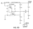
- FIGS. 5A through 5G are schematic diagrams of exemplary implementations of a high voltage input capacitor balancing and startup circuit.
- an exemplary implementation of a high voltage input capacitor balancing and startup circuit 400 can provide active balance for two input capacitor configuration (capacitors 414 , 416 (also labeled C 1 , C 2 , respectively)) used as an input filter for a power supply.
- High voltage input capacitor balancing circuit 400 can also provide startup voltage for the controller 440 in the power supply.
- high voltage input capacitor balancing circuit 400 includes voltage divider 410 and an X1 (“times one”) buffer 412 .
- the X1 buffer 412 can be packaged in an SOIC (small-outline integrated circuit) package with 8 pins.
- Voltage divider 410 can be implemented with resistors 420 , 424 , 426 , and 428 (also labeled R 1 , R 2 , R 3 , and R 4 , respectively) having values which provide the desired lower bleed current (e.g., one-fifth to one-twentieth the normal required bleed current).
- FIG. 5B is a schematic diagram of an exemplary implementation of high voltage input capacitor balancing and startup circuit 500 according to an embodiment of the invention.
- High voltage input capacitor balancing circuit 500 can provide active balance for a three input capacitor configuration (capacitors 514 , 516 , and 518 (also labeled C 1 , C 2 , and C 3 , respectively)) used as an input filter for a power supply.
- High voltage input capacitor balancing circuit 500 can also provide startup voltage for the controller 540 in a power supply.
- high voltage input capacitor balancing and startup circuit 500 comprises a plurality of X1 (“times one”) buffers 512 , which are coupled to voltage divider 510 (implemented with resistors 520 , 522 , 524 , 526 , 528 , and 530 (also labeled R 1 , R 2 , R 3 , R 4 , R 5 , and R 6 , respectively)).
- FIG. 5C illustrates, that components of, or multiple start up and balance circuits, can be stacked in a similar manner to the input capacitors to provide capacitor balance for any number of input capacitors or input voltage.
- four input capacitors would require three start up and balance circuits in stacked arrangement.
- Six input capacitors would require five stacked start up and balance circuits.
- M ⁇ 1 number of start-up and balance circuits may be provided.
- high voltage input capacitor balancing circuit 600 includes voltage divider 610 and two X1 (“times one”) buffers 612 .
- each X1 buffer 612 can be packaged in an SOIC package with 8 pins.
- the X1 buffer 612 can be stacked to balance input capacitors 614 , 616 , and 618 (also labeled C 1 , C 2 , and C 3 , respectively).
- Voltage divider 610 can be implemented with resistors 620 , 622 , 624 , 626 , 628 , and 630 (also labeled R 1 , R 2 , R 3 , R 4 , R 5 , and R 6 , respectively) having values which provide the desired lower bleed current (e.g., one-fifth to one-twentieth the normal required bleed current).
- FIGS. 5D through 5G are schematic diagrams of further exemplary implementation of input capacitor balancing and startup circuits, according to embodiments of the invention.
- Capacitive balancing may also be an issue at low voltages when using high capacitive value capacitors such as “Supercapacitors” or “Supercaps.”
- Supercaps typically have voltage ratings typically below 6 volts, and so must be stacked to increase the voltage at which they can function.
- low voltage capacitors, such as Supercaps are very sensitive to over-voltage and thus must be balanced carefully.
- the energy storage capacity of such capacitors is very high so the resistive balancing methodology may be inappropriate especially during charge and discharge.
- low voltage capacitors are balanced without excessive bleed current, thereby increasing power supply efficiency.
- Such embodiment can reduce the traditional divider losses by up to 90% or more.
- FIG. 6 is a schematic diagram of an exemplary implementation of a possible supercapacitor balancing circuit employing operational amplifiers (“op-amps”).
- op-amps operational amplifiers
- Such a circuit could be used or incorporated in a device, such as, for example, smart meter output voltage storage that is subject to, or used in, a wide range of applications.
- the circuit of FIG. 6 can be connected to a power source at an input terminal and operate with a wide range of input voltages, for example, approximately 6 to 20V DC.
- These balancing circuits can be stacked along with additional capacitors for higher voltage applications.
- Similar circuits can also be used at high voltages using appropriate op-amps, in which case, the operating voltages could range from 1 volt to more than 1000 volts.
- the circuit includes low voltage capacitors 714 , 716 , and 718 (also labeled C 1 , C 2 , and C 3 , respectively) in stacked arrangement.
- Each capacitor 714 , 716 , and 718 may have high energy storage capacity and relatively low voltage rating.
- These capacitors can each be implemented with a Supercapacitor.
- Resistors 720 , 722 , and 724 (also labeled as R 1 , R 2 , and R 3 , respectively) form a voltage divider 710 that (evenly) divides the input voltage VIN among the three stacked capacitors 714 , 716 , and 718 .
- Resistors 709 and 711 limits the drive current provided to balance capacitors 714 , 716 , and 718 .
- Operational amplifiers 750 and 752 also labeled U 1 a and U 1 b , respectively, each of which can be implemented as a buffer amplifier (e.g., with approximately ⁇ 1 gain), provide the balancing current. With this arrangement, the low voltage capacitors 714 , 716 , and 718 can be used at higher voltages and in many applications where they previously could not be used.
- FIG. 7 is a schematic diagram of an exemplary implementation of a high voltage input capacitor balancing circuit 800 according to an embodiment of the invention.
- FIG. 7 shows how to use the circuit to start a controller not equipped for high voltage (HV) start up.
- the circuit 800 is used to provide a buffered voltage which is approximately one-half of Vin to the collector of a transistor 802 (also labeled Q 1 ), which in one embodiment (as shown) can be a BJT.
- the emitter of transistor 802 is connected to a resistor 804 (also labeled R 6 ) which in turn is connected to the Vcc pin of a power supply controller.
- the base of transistor 802 is connected to a zener diode 806 (also labeled D 1 ) and to the bottom of the chain of resistors 808 , 810 , 812 , and 814 (also labeled R 1 , R 2 , R 3 , and R 4 , respectively).
- the top of the resistor chain is connected to Vin.
- Resistors 808 through 814 can be of equal value. Vin, less the voltage of diode 806 , is divided across resistors 808 - 814 and provides an approximate midpoint value of Vin to pin 4 of the X1 buffer 816 .
- the voltage at pin 5 of the buffer is roughly one fourth of Vin plus 3 ⁇ 4 of the voltage on diode 806 .
- Vin produces a current flow through the resistors 808 - 814 and the zener diode 806 .
- the current drops voltage across the zener diode 806 .
- This voltage is applied to the base of transistor 802 . If the voltage at the base of transistor 802 is approximately 0.7 volts more positive than the voltage on Vcc, transistor 802 will turn on and charge the Vcc capacitor.
- the current through transistor 802 is limited by resistor 804 .
- the maximum current is determined by the maximum voltage difference between the voltage at the emitter of transistor 802 divided by the value of resistor 804 . When the voltage on Vcc is less than that required to cause the BJT to turn on, transistor 802 turns off.
- Vcc would be charged to a high enough voltage for the power supply controller to turn on. The action of the power supply would then supply the needed current to continue to charge and maintain Vcc. Thus, once the startup circuit has charged Vcc to a value sufficient for the controller to function, the start up circuit is no longer required during regular power supply operation.
- Resistor 818 also labeled R 5
- capacitor 820 also labeled C 1
- Buffer 816 can be made up of any combination of suitable devices, such as BJTs, JFETs, MOSFETS, as understood by one of ordinary skill.
- the X1 buffer 816 as shown in FIG. 7 is one possible implementation for providing one half Vin to the transistor 802 .
- this buffer might also be realized or implemented in other ways, such as a single BJT or MOSFET or a combination of BJTs and/or MOSFETs.
Landscapes
- Engineering & Computer Science (AREA)
- Power Engineering (AREA)
- Dc-Dc Converters (AREA)
- Direct Current Feeding And Distribution (AREA)
Abstract
Description
Claims (13)
Priority Applications (1)
| Application Number | Priority Date | Filing Date | Title |
|---|---|---|---|
| US13/347,616 US8971069B2 (en) | 2010-08-11 | 2012-01-10 | Startup circuit and input capacitor balancing circuit |
Applications Claiming Priority (4)
| Application Number | Priority Date | Filing Date | Title |
|---|---|---|---|
| US37279310P | 2010-08-11 | 2010-08-11 | |
| US201161431723P | 2011-01-11 | 2011-01-11 | |
| US13/207,798 US8638575B2 (en) | 2010-08-11 | 2011-08-11 | High voltage startup circuit |
| US13/347,616 US8971069B2 (en) | 2010-08-11 | 2012-01-10 | Startup circuit and input capacitor balancing circuit |
Publications (2)
| Publication Number | Publication Date |
|---|---|
| US20120176821A1 US20120176821A1 (en) | 2012-07-12 |
| US8971069B2 true US8971069B2 (en) | 2015-03-03 |
Family
ID=46455105
Family Applications (1)
| Application Number | Title | Priority Date | Filing Date |
|---|---|---|---|
| US13/347,616 Active 2032-08-24 US8971069B2 (en) | 2010-08-11 | 2012-01-10 | Startup circuit and input capacitor balancing circuit |
Country Status (2)
| Country | Link |
|---|---|
| US (1) | US8971069B2 (en) |
| CN (1) | CN102710114B (en) |
Cited By (3)
| Publication number | Priority date | Publication date | Assignee | Title |
|---|---|---|---|---|
| CN105515381A (en) * | 2016-01-27 | 2016-04-20 | 南京能瑞电力科技有限公司 | Multi-level converter direct-current side voltage balancing circuit |
| US9812986B2 (en) * | 2016-03-29 | 2017-11-07 | Lsis Co., Ltd. | Apparatus for balancing voltages of DC link capacitor in inverter |
| US11736103B2 (en) | 2021-06-16 | 2023-08-22 | Appleton Grp Llc | Voltage source kickstart circuit for powering integrated circuits |
Families Citing this family (6)
| Publication number | Priority date | Publication date | Assignee | Title |
|---|---|---|---|---|
| DE102012109283A1 (en) * | 2012-09-28 | 2014-04-03 | Siemens Aktiengesellschaft | Power converter of electrical machine used for feeding three-phase motor of motor vehicle, has electrical resistance that is provided in circuit portion at same time through decoupling element |
| US10903663B2 (en) | 2017-06-30 | 2021-01-26 | Avx Corporation | Balancing circuit for an ultracapacitor module |
| CN110870160B (en) | 2017-07-21 | 2024-01-26 | 京瓷Avx元器件公司 | Balancing circuit for an electrical energy storage device |
| CN111614258B (en) * | 2020-06-16 | 2021-08-17 | 任守华 | High-voltage generator based on MOS tube series discharge |
| CN117549743A (en) * | 2023-11-09 | 2024-02-13 | 阳光电源股份有限公司 | Hot plug protection slow start circuit and battery management system |
| CN120749978B (en) * | 2025-09-04 | 2025-11-18 | 深圳市复兴伟业技术有限公司 | Capacitor-based photovoltaic circuits, low-energy-loss methods, and home controllers |
Citations (4)
| Publication number | Priority date | Publication date | Assignee | Title |
|---|---|---|---|---|
| US5682022A (en) * | 1995-05-11 | 1997-10-28 | Otis Elevator Company | Active stabilization of serially connected capacitors in high voltage applications |
| US20030214267A1 (en) * | 2002-05-20 | 2003-11-20 | Long Laurence P. | Ultracapacitor balancing circuit |
| US6738277B2 (en) * | 2001-11-27 | 2004-05-18 | Power Integrations, Inc. | Method and apparatus for balancing active capacitor leakage current |
| US20080007891A1 (en) * | 2004-02-17 | 2008-01-10 | Cooper Technologies Company | Active balancing circuit modules, systems and capacitor devices |
-
2012
- 2012-01-10 US US13/347,616 patent/US8971069B2/en active Active
- 2012-01-11 CN CN201210061724.8A patent/CN102710114B/en active Active
Patent Citations (4)
| Publication number | Priority date | Publication date | Assignee | Title |
|---|---|---|---|---|
| US5682022A (en) * | 1995-05-11 | 1997-10-28 | Otis Elevator Company | Active stabilization of serially connected capacitors in high voltage applications |
| US6738277B2 (en) * | 2001-11-27 | 2004-05-18 | Power Integrations, Inc. | Method and apparatus for balancing active capacitor leakage current |
| US20030214267A1 (en) * | 2002-05-20 | 2003-11-20 | Long Laurence P. | Ultracapacitor balancing circuit |
| US20080007891A1 (en) * | 2004-02-17 | 2008-01-10 | Cooper Technologies Company | Active balancing circuit modules, systems and capacitor devices |
Non-Patent Citations (1)
| Title |
|---|
| IBM Technical Disclosure Bulletin NB84092320, Capacitive Start-Up Circuit for Switching Power Supply, Sep. 1, 1984, vol. 27, Issue No. 4B, p. 2320. * |
Cited By (3)
| Publication number | Priority date | Publication date | Assignee | Title |
|---|---|---|---|---|
| CN105515381A (en) * | 2016-01-27 | 2016-04-20 | 南京能瑞电力科技有限公司 | Multi-level converter direct-current side voltage balancing circuit |
| US9812986B2 (en) * | 2016-03-29 | 2017-11-07 | Lsis Co., Ltd. | Apparatus for balancing voltages of DC link capacitor in inverter |
| US11736103B2 (en) | 2021-06-16 | 2023-08-22 | Appleton Grp Llc | Voltage source kickstart circuit for powering integrated circuits |
Also Published As
| Publication number | Publication date |
|---|---|
| CN102710114B (en) | 2015-11-25 |
| US20120176821A1 (en) | 2012-07-12 |
| CN102710114A (en) | 2012-10-03 |
Similar Documents
| Publication | Publication Date | Title |
|---|---|---|
| US8971069B2 (en) | Startup circuit and input capacitor balancing circuit | |
| US8638575B2 (en) | High voltage startup circuit | |
| US8929107B2 (en) | Active surge protection in a power supply | |
| US9438108B2 (en) | Bias voltage generating circuit and switching power supply thereof | |
| He | A novel quasi-resonant bridge modular switched-capacitor converter with enhanced efficiency and reduced output voltage ripple | |
| US7167028B2 (en) | Voltage detection circuit, power supply unit and semiconductor device | |
| CN103066817A (en) | Ripple suppression circuit, power supply system thereof and ripple suppression method | |
| CN107251398A (en) | DC‑DC Converter | |
| CN117769798A (en) | Multilevel structures and methods for switch mode power supplies | |
| CN102377327B (en) | High-voltage starting circuit | |
| CN102104325A (en) | Power factor converter and method | |
| US10159125B1 (en) | LED power supply device | |
| CN202997919U (en) | Ripple suppression circuit and power supply system thereof | |
| KR20080110376A (en) | Multi-output adapter | |
| US10143046B2 (en) | Light emitting diode driver with differential voltage supply | |
| CN103580508A (en) | Ac/dc converter circuit | |
| US20250070641A1 (en) | Power conversion circuit and method | |
| JP2014033553A (en) | Dc-dc power conversion device and power conditioner for photovoltaic power generation system | |
| KR20160124588A (en) | LED power supply control circuit | |
| US9960636B2 (en) | Power supply system and direct-current converter thereof | |
| US11165348B2 (en) | Boost converter with high output efficiency | |
| US20180367041A1 (en) | Dual-Capacitors-Based AC Line Frequency Low Voltage DC Power Supply Circuit | |
| CN209402761U (en) | A kind of overvoltage crowbar suitable for LED constant current power supply | |
| CN110995010B (en) | Power supply conversion device | |
| TW202537209A (en) | Integrated circuit, method and circuit for operating multi- level converter circuits |
Legal Events
| Date | Code | Title | Description |
|---|---|---|---|
| AS | Assignment |
Owner name: FAIRCHILD SEMICONDUCTOR CORPORATION, CALIFORNIA Free format text: ASSIGNMENT OF ASSIGNORS INTEREST;ASSIGNOR:DUNIPACE, RICHARD A.;REEL/FRAME:032903/0928 Effective date: 20120109 |
|
| STCF | Information on status: patent grant |
Free format text: PATENTED CASE |
|
| AS | Assignment |
Owner name: DEUTSCHE BANK AG NEW YORK BRANCH, AS COLLATERAL AGENT, NEW YORK Free format text: PATENT SECURITY AGREEMENT;ASSIGNOR:FAIRCHILD SEMICONDUCTOR CORPORATION;REEL/FRAME:040075/0644 Effective date: 20160916 Owner name: DEUTSCHE BANK AG NEW YORK BRANCH, AS COLLATERAL AG Free format text: PATENT SECURITY AGREEMENT;ASSIGNOR:FAIRCHILD SEMICONDUCTOR CORPORATION;REEL/FRAME:040075/0644 Effective date: 20160916 |
|
| MAFP | Maintenance fee payment |
Free format text: PAYMENT OF MAINTENANCE FEE, 4TH YEAR, LARGE ENTITY (ORIGINAL EVENT CODE: M1551); ENTITY STATUS OF PATENT OWNER: LARGE ENTITY Year of fee payment: 4 |
|
| AS | Assignment |
Owner name: SEMICONDUCTOR COMPONENTS INDUSTRIES, LLC, ARIZONA Free format text: ASSIGNMENT OF ASSIGNORS INTEREST;ASSIGNOR:FAIRCHILD SEMICONDUCTOR CORPORATION;REEL/FRAME:057694/0374 Effective date: 20210722 Owner name: SEMICONDUCTOR COMPONENTS INDUSTRIES, LLC, ARIZONA Free format text: ASSIGNMENT OF ASSIGNOR'S INTEREST;ASSIGNOR:FAIRCHILD SEMICONDUCTOR CORPORATION;REEL/FRAME:057694/0374 Effective date: 20210722 |
|
| AS | Assignment |
Owner name: FAIRCHILD SEMICONDUCTOR CORPORATION, ARIZONA Free format text: RELEASE BY SECURED PARTY;ASSIGNOR:DEUTSCHE BANK AG NEW YORK BRANCH;REEL/FRAME:057969/0206 Effective date: 20211027 Owner name: FAIRCHILD SEMICONDUCTOR CORPORATION, ARIZONA Free format text: RELEASE OF SECURITY INTEREST;ASSIGNOR:DEUTSCHE BANK AG NEW YORK BRANCH;REEL/FRAME:057969/0206 Effective date: 20211027 |
|
| AS | Assignment |
Owner name: DEUTSCHE BANK AG NEW YORK BRANCH, AS COLLATERAL AGENT, NEW YORK Free format text: SECURITY INTEREST;ASSIGNOR:SEMICONDUCTOR COMPONENTS INDUSTRIES, LLC;REEL/FRAME:058871/0799 Effective date: 20211028 |
|
| MAFP | Maintenance fee payment |
Free format text: PAYMENT OF MAINTENANCE FEE, 8TH YEAR, LARGE ENTITY (ORIGINAL EVENT CODE: M1552); ENTITY STATUS OF PATENT OWNER: LARGE ENTITY Year of fee payment: 8 |
|
| AS | Assignment |
Owner name: FAIRCHILD SEMICONDUCTOR CORPORATION, ARIZONA Free format text: RELEASE OF SECURITY INTEREST IN PATENTS RECORDED AT REEL 040075, FRAME 0644;ASSIGNOR:DEUTSCHE BANK AG NEW YORK BRANCH, AS COLLATERAL AGENT;REEL/FRAME:064070/0536 Effective date: 20230622 Owner name: SEMICONDUCTOR COMPONENTS INDUSTRIES, LLC, ARIZONA Free format text: RELEASE OF SECURITY INTEREST IN PATENTS RECORDED AT REEL 040075, FRAME 0644;ASSIGNOR:DEUTSCHE BANK AG NEW YORK BRANCH, AS COLLATERAL AGENT;REEL/FRAME:064070/0536 Effective date: 20230622 |
|
| AS | Assignment |
Owner name: FAIRCHILD SEMICONDUCTOR CORPORATION, ARIZONA Free format text: RELEASE OF SECURITY INTEREST IN PATENTS RECORDED AT REEL 058871, FRAME 0799;ASSIGNOR:DEUTSCHE BANK AG NEW YORK BRANCH, AS COLLATERAL AGENT;REEL/FRAME:065653/0001 Effective date: 20230622 Owner name: SEMICONDUCTOR COMPONENTS INDUSTRIES, LLC, ARIZONA Free format text: RELEASE OF SECURITY INTEREST IN PATENTS RECORDED AT REEL 058871, FRAME 0799;ASSIGNOR:DEUTSCHE BANK AG NEW YORK BRANCH, AS COLLATERAL AGENT;REEL/FRAME:065653/0001 Effective date: 20230622 |