EP2704536A1 - Method for producing a circuit board system - Google Patents
Method for producing a circuit board system Download PDFInfo
- Publication number
- EP2704536A1 EP2704536A1 EP20120182566 EP12182566A EP2704536A1 EP 2704536 A1 EP2704536 A1 EP 2704536A1 EP 20120182566 EP20120182566 EP 20120182566 EP 12182566 A EP12182566 A EP 12182566A EP 2704536 A1 EP2704536 A1 EP 2704536A1
- Authority
- EP
- European Patent Office
- Prior art keywords
- circuit board
- solder
- metallization layer
- soldering
- electronic components
- Prior art date
- Legal status (The legal status is an assumption and is not a legal conclusion. Google has not performed a legal analysis and makes no representation as to the accuracy of the status listed.)
- Granted
Links
Images





Classifications
-
- H—ELECTRICITY
- H05—ELECTRIC TECHNIQUES NOT OTHERWISE PROVIDED FOR
- H05K—PRINTED CIRCUITS; CASINGS OR CONSTRUCTIONAL DETAILS OF ELECTRIC APPARATUS; MANUFACTURE OF ASSEMBLAGES OF ELECTRICAL COMPONENTS
- H05K1/00—Printed circuits
- H05K1/02—Details
- H05K1/0201—Thermal arrangements, e.g. for cooling, heating or preventing overheating
- H05K1/0203—Cooling of mounted components
-
- H—ELECTRICITY
- H05—ELECTRIC TECHNIQUES NOT OTHERWISE PROVIDED FOR
- H05K—PRINTED CIRCUITS; CASINGS OR CONSTRUCTIONAL DETAILS OF ELECTRIC APPARATUS; MANUFACTURE OF ASSEMBLAGES OF ELECTRICAL COMPONENTS
- H05K1/00—Printed circuits
- H05K1/02—Details
- H05K1/0201—Thermal arrangements, e.g. for cooling, heating or preventing overheating
- H05K1/0203—Cooling of mounted components
- H05K1/0204—Cooling of mounted components using means for thermal conduction connection in the thickness direction of the substrate
-
- H—ELECTRICITY
- H05—ELECTRIC TECHNIQUES NOT OTHERWISE PROVIDED FOR
- H05K—PRINTED CIRCUITS; CASINGS OR CONSTRUCTIONAL DETAILS OF ELECTRIC APPARATUS; MANUFACTURE OF ASSEMBLAGES OF ELECTRICAL COMPONENTS
- H05K1/00—Printed circuits
- H05K1/02—Details
- H05K1/0213—Electrical arrangements not otherwise provided for
- H05K1/0237—High frequency adaptations
- H05K1/024—Dielectric details, e.g. changing the dielectric material around a transmission line
-
- H—ELECTRICITY
- H05—ELECTRIC TECHNIQUES NOT OTHERWISE PROVIDED FOR
- H05K—PRINTED CIRCUITS; CASINGS OR CONSTRUCTIONAL DETAILS OF ELECTRIC APPARATUS; MANUFACTURE OF ASSEMBLAGES OF ELECTRICAL COMPONENTS
- H05K13/00—Apparatus or processes specially adapted for manufacturing or adjusting assemblages of electric components
- H05K13/04—Mounting of components, e.g. of leadless components
- H05K13/046—Surface mounting
- H05K13/0465—Surface mounting by soldering
-
- H—ELECTRICITY
- H05—ELECTRIC TECHNIQUES NOT OTHERWISE PROVIDED FOR
- H05K—PRINTED CIRCUITS; CASINGS OR CONSTRUCTIONAL DETAILS OF ELECTRIC APPARATUS; MANUFACTURE OF ASSEMBLAGES OF ELECTRICAL COMPONENTS
- H05K3/00—Apparatus or processes for manufacturing printed circuits
- H05K3/30—Assembling printed circuits with electric components, e.g. with resistors
- H05K3/32—Assembling printed circuits with electric components, e.g. with resistors electrically connecting electric components or wires to printed circuits
- H05K3/34—Assembling printed circuits with electric components, e.g. with resistors electrically connecting electric components or wires to printed circuits by soldering
- H05K3/3465—Application of solder
- H05K3/3485—Application of solder paste, slurry or powder
-
- H—ELECTRICITY
- H10—SEMICONDUCTOR DEVICES; ELECTRIC SOLID-STATE DEVICES NOT OTHERWISE PROVIDED FOR
- H10W—GENERIC PACKAGES, INTERCONNECTIONS, CONNECTORS OR OTHER CONSTRUCTIONAL DETAILS OF DEVICES COVERED BY CLASS H10
- H10W40/00—Arrangements for thermal protection or thermal control
- H10W40/70—Fillings or auxiliary members in containers or in encapsulations for thermal protection or control
-
- H—ELECTRICITY
- H10—SEMICONDUCTOR DEVICES; ELECTRIC SOLID-STATE DEVICES NOT OTHERWISE PROVIDED FOR
- H10W—GENERIC PACKAGES, INTERCONNECTIONS, CONNECTORS OR OTHER CONSTRUCTIONAL DETAILS OF DEVICES COVERED BY CLASS H10
- H10W42/00—Arrangements for protection of devices
- H10W42/20—Arrangements for protection of devices protecting against electromagnetic or particle radiation, e.g. light, X-rays, gamma-rays or electrons
-
- H—ELECTRICITY
- H10—SEMICONDUCTOR DEVICES; ELECTRIC SOLID-STATE DEVICES NOT OTHERWISE PROVIDED FOR
- H10W—GENERIC PACKAGES, INTERCONNECTIONS, CONNECTORS OR OTHER CONSTRUCTIONAL DETAILS OF DEVICES COVERED BY CLASS H10
- H10W70/00—Package substrates; Interposers; Redistribution layers [RDL]
- H10W70/01—Manufacture or treatment
- H10W70/05—Manufacture or treatment of insulating or insulated package substrates, or of interposers, or of redistribution layers
- H10W70/093—Connecting or disconnecting other interconnections thereto or therefrom, e.g. connecting bond wires or bumps
-
- H—ELECTRICITY
- H05—ELECTRIC TECHNIQUES NOT OTHERWISE PROVIDED FOR
- H05K—PRINTED CIRCUITS; CASINGS OR CONSTRUCTIONAL DETAILS OF ELECTRIC APPARATUS; MANUFACTURE OF ASSEMBLAGES OF ELECTRICAL COMPONENTS
- H05K2201/00—Indexing scheme relating to printed circuits covered by H05K1/00
- H05K2201/10—Details of components or other objects attached to or integrated in a printed circuit board
- H05K2201/10227—Other objects, e.g. metallic pieces
- H05K2201/10371—Shields or metal cases
-
- H—ELECTRICITY
- H05—ELECTRIC TECHNIQUES NOT OTHERWISE PROVIDED FOR
- H05K—PRINTED CIRCUITS; CASINGS OR CONSTRUCTIONAL DETAILS OF ELECTRIC APPARATUS; MANUFACTURE OF ASSEMBLAGES OF ELECTRICAL COMPONENTS
- H05K2203/00—Indexing scheme relating to apparatus or processes for manufacturing printed circuits covered by H05K3/00
- H05K2203/15—Position of the PCB during processing
- H05K2203/1572—Processing both sides of a PCB by the same process; Providing a similar arrangement of components on both sides; Making interlayer connections from two sides
-
- H—ELECTRICITY
- H10—SEMICONDUCTOR DEVICES; ELECTRIC SOLID-STATE DEVICES NOT OTHERWISE PROVIDED FOR
- H10W—GENERIC PACKAGES, INTERCONNECTIONS, CONNECTORS OR OTHER CONSTRUCTIONAL DETAILS OF DEVICES COVERED BY CLASS H10
- H10W90/00—Package configurations
- H10W90/701—Package configurations characterised by the relative positions of pads or connectors relative to package parts
- H10W90/721—Package configurations characterised by the relative positions of pads or connectors relative to package parts of bump connectors
- H10W90/724—Package configurations characterised by the relative positions of pads or connectors relative to package parts of bump connectors between a chip and a stacked insulating package substrate, interposer or RDL
Definitions
- circuit board system as can be used, for instance, in an infotainment head unit or in a telematic unit, and a method for producing a circuit board system.
- a first circuit board with a top side, a bottom side, a top metallization layer arranged at the top side, and a bottom metallization layer arranged at the bottom side.
- the bottom metallization layer includes a number of soldering pads.
- a first solder is applied over the soldering pads and a second solder is applied over the top metallization layer.
- Also provided are a number of electronic components, and a metallic or metallized shielding frame that has an opening. The number of electronic components and the shielding frame are arranged on the applied second solder and soldered to the top metallization layer by melting the second solder and by subsequently cooling of the second solder to below its solidification temperature. After cooling, a thermal interface material is applied through the opening over the top side of at least one of the electronic components.
- a housing cover with an electrically conductive surface may be attached to the first circuit board such that the contact springs electrically contact the housing cover and that the thermal interface material mechanically contacts the housing cover and at least one of the electronic components.
- a second circuit board with a top side, a bottom side and a top metallization layer arranged at the top side is provided.
- the soldering pads are electrically and mechanically connected to the top metallization layer of the second circuit board by soldering.
- FIG. 1 illustrates a circuit board system 100 with a first circuit board 1.
- the first circuit board 1 has a top side 11 and a bottom side 12.
- a top metallization layer 13 is arranged at the top side 11 and a bottom metallization layer 14 is arranged at the bottom side 12.
- a number of soldering pads 141 are formed in the bottom metallization layer 14.
- a first solder 16 is arranged on the soldering pads 141 such that the first solder 16 completely covers the soldering pads 141.
- a number of electronic components 17 and a shielding frame 18 are soldered to the top metallization layer 13 using a second solder 15.
- a spring frame 19, which has an electrically conductive surface and several electrically conductive contact springs 191, is snapped onto the shielding frame 18.
- such a circuit board system 100 may be, prior to or after snapping the spring frame 19 onto the shielding frame 18, soldered together with other electronic components to a second circuit board.
- a circuit board arrangement may form an infotainment head unit or a telematic unit of a vehicle.
- the invention is not limited to infotainment head units or telematic units and/or the use in vehicles.
- FIG. 2 is a bottom view of the first circuit board 1 of the circuit board system 100.
- no first solder 16 is applied over the soldering pads 141.
- the soldering pads 141 are formed in the bottom metallization layer 14.
- the cross-sectional plane E1 which corresponds to the view of FIG. 1 .
- the bottom metallization layer 14 is protected with a solder mask 10.
- the solder mask 10 exists but is not shown in FIG. 1 .
- the bottom metallization layer 14 also includes conductor lines for electrically connecting the soldering pads 141. However, the conductor lines are covered by the solder mask 10 and therefore hidden in FIG. 2 .
- the soldering pads 141 may have different sizes. The size may depend on the required capacity & inductance. A first subset of the soldering pads 141 may have a first pitch p1, for instance at least 2,4 mm, and a second subset of the soldering pads 141 may have a second pitch p2, for instance at least 3 mm. The total number of soldering pads 141 has a total surface area A141 tot . In this regard, the surface of a soldering pad 141 is the area of the footprint of the pad 141.
- the first circuit board 1 itself has a footprint of w1 (length) x w2 (width) which may be, for instance, less than or equal to 70 mm x 70 mm. However, the footprint may also exceed the size of 70 mm x 70 mm, that is, the length w1 and the width w2 may each be more than 70 mm.
- the corner regions of the first circuit board 1 may optionally be free of soldering pads 141, which is also illustrated in FIG. 2 .
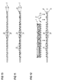
- FIG. 3 shows an exploded view of the circuit board system 100 of FIG. 1 .
- the top and bottom metallization layers 13, 14 form integral parts of the first circuit board 1.
- a first solder 16 e.g. a soldering paste
- FIG. 4 the first circuit board 1 with the first solder 16 applied over the soldering pads 141 is arranged in a reflow soldering machine 300 in which the first solder 16 is melted and subsequently cooled to below its solidification temperature.
- the soldering pads 141 are plated with the first solder 16, for instance a solder depot, such that the first circuit board 1 can be handled without the risk of wearing the soldering paste away.
- Applying the first solder 16 may be carried out using screen printing, stencil printing or jet printing.
- the first circuit board 1 is removed from the reflow soldering machine 300 and a second solder 15, e.g. a soldering paste, is applied over the top metallization 13, for instance by means of dispensing, screen printing or mask printing.
- a second solder 15 e.g. a soldering paste
- FIG. 6 a number of electronic components 17 and a shielding frame 18 are arranged on the applied second solder 15, that is, on the soldering paste, see FIG. 7 .
- the shielding frame 18 may consist of or include nickel (Ni) and/or silver (Ag), or consist of or include an alloy of both nickel (Ni) and silver (Ag).
- the first circuit board 1 with the number of electronic components 17 and the shielding frame 18 arranged on the applied second solder 15, i.e. the soldering paste, is arranged in the same or a further reflow soldering machine 300 in which the number of electronic components 17 and the shielding frame 18 are soldered to the top metallization layer 13 by melting the second solder 16 and subsequently cooling the melted solder 16 to below its solidification temperature.
- the first circuit board 1 with the number of electronic components 17 and the shielding frame 18 soldered to the top metallization layer 13 may be removed from the reflow soldering machine 300.
- the result is an electronic subunit 100 which may be soldered to a second circuit board in order to form a circuit board arrangement.
- the spring frame 19 Prior to or after soldering the electronic subunit to a second circuit board, the spring frame 19 is snapped onto the shielding frame 18.
- FIG. 9 shows the subunit 100 with the spring frame 19 snapped onto the shielding frame 18.
- a circuit board arrangement 200 ( FIG. 16 ) can be produced by soldering.
- a second circuit board 2 as exemplarily illustrated in FIG. 10 is provided.
- the second circuit board 2 has a top side 21 and a bottom side 22.
- a top metallization layer 23 is arranged at the top side 21 and an optional bottom metallization layer 24 is arranged at the bottom side 12.
- a third solder 25 e.g. a soldering paste
- a third solder 25 is applied over the top metallization layer 23, for instance by means of dispensing, screen printing or mask printing.
- the result is illustrated in FIG. 11 .
- the subunit 100 as described above and one ore more further arbitrary electronic components 27 are arranged on the applied third solder 25, for instance in a pick-and-place process.
- the second circuit board 2 with the third solder 25 and the subunit 100 and the further arbitrary electronic components 27 arranged on the third solder 25 are arranged in one of the previous or a further reflow soldering machine 300, see FIG.
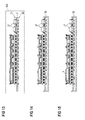
- the soldered arrangement may be removed from the reflow soldering machine 300 and optionally be mounted in a bottom housing 32, see FIG. 14 .
- a subunit which includes the first circuit board 1 with the top metallization layer 13 and the bottom metallization layer 14, the first solder 16, the second solder 15 and the number of electronic components 17 but not the shielding frame 18, the thermal interface material 4 and the housing cover 31, may have a weight such that the ratio between the mass of the subunit and the total surface area A141 tot is less than or equal to 0,08 g/mm 2 .
- This allows soldering further electronic components to the bottom metallization 24 of the bottom metallization layer 24 of the second circuit board 2 with the subunit already soldered to the top metallization layer 23 and with the second circuit board 2 top side 23 down (i.e. facing towards earth) in a reflow soldering process. Due to the low weight of such a subunit, it will not drop down from the second circuit board 2.
- a thermal interface material 4 for instance a thermal interface paste or a self-adhesive thermal interface pad, is arranged on the top side of at least one of the electronic components 17, that is, on that side of the respective at least one electronic component 17 facing away from the first circuit board 1, see FIG. 15 .
- the thermal interface material 4 is applied after the last of all above mentioned soldering processes, as far as such soldering processes are used.
- the thermal interface material 4 may be arranged on the respective electronic components 17 prior to or after snapping the spring frame 19 onto the shielding frame 18.
- a housing cover 31 with an electrically conductive surface is attached to the first circuit board 1 such that the contact springs 191 of the spring frame 19 electrically contact the housing cover 31, and that the thermal interface material 4 mechanically contacts the housing cover 31 and at least one of the electronic components 17.
- the electronic components 17 provided with the thermal interface material 4 are efficiently cooled by the housing cover 31.
- the housing cover 31 acts both as a heat sink and, due to its electrically conductive surface, as an electromagnetic shielding.
- the housing cover 31 may be made of a bent thin sheet-metal with a thickness D19 (see FIG. 3 ), for instance 0,1 mm to 0,2 mm, e.g. about 0,15 mm.
- FIG. 17 is an enlarged view of a section S1 of the first circuit board 1 illustrated in FIG. 3 .
- the bottom metallization layer 14 includes soldering pads 141 and conductive lines 142.
- the conductive lines 142 serve to electrically connect the soldering pads 141.
- a solder mask 10 covers the conductive lines 142 but not the soldering pads 141.
- Metallic vias 134 are used to electrically interconnect different metallization layers 13, 14 of the first circuit board 1.
- the first circuit board 1 may include one or more additional metallization layers between the top metallization layer 13 and the bottom metallization layer 14.
- a first circuit board 1 may have, including the top and bottom metallization layers 13, 14, four or eight metallization layers, one above the other.
- metallic vias 134 may be used to electrically interconnect any two of the metallization layers of the first circuit board 1.
- none of all metallic vias 134 of the first circuit board 1 is formed in the area of a soldering pad 141 of the bottom metallization layer 14.
- any electric connection between a metallic via 134 of the first circuit board 1 and a soldering pad 141 of the bottom metallization 14 is realized via a conductor line 142 formed in the bottom metallization layer 14.
- a via may be formed in the area of a soldering pad 141, then filled with electrically conductive material, and grinded in order to achieve a flat surface of the soldering pad 141.
- FIG. 18 is an enlarged view of a section S2 of the first circuit board 1 illustrated in FIG. 6 .
- the sections S1 and S2 are identical, however, in the arrangement of FIGs. 6 and 18 (S2) there is a first solder 16 applied over the soldering pads 141 and a second solder 15 applied over the top metallization layer 13. Although the second solder 15 is still present as a paste, the first solder 16 has already undergone a reflow and a subsequent cooling and solidification process as described above with reference to FIGs. 4 and 5 .
- the (structured) first solder layer 16 may have an average thickness D16 of at least 100 ⁇ m.
- the distance d2 between the plane E2 and that section of the first solder 16 arranged above the respective soldering pad 141 is less than 100 ⁇ m.
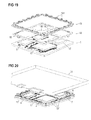
- FIG. 19 again shows an exploded view of a circuit board system 100 as explained above.
- the shielding frame 18 may include a ring-shaped section and a cross-like section 181 arranged inside the ring-shaped section.
- the cross-like section 181 may be used in a pick-and-place process, in which the shielding frame 18 is placed on the second solder 15 as described above with reference to FIG. 7 .
- the cross-like section 181 may include a point of application which is used by a pick-and-place machine in the pick-and-place process.
- FIG. 20 shows the arrangement of FIG 19 in the assembled state, with a thermal interface material 4 applied over the top sides of some of the electronic components 17 and with a housing cover 31 to be mounted on the circuit board system 100.
- FIG. 21 is a perspective view of a further example of a first circuit board 1 that is populated with a number of electronic components.
- a shielding frame 18 with several openings 20 is soldered to the first circuit board 1.
- electronic components such as processors, power transistors etc. with flat large area top sides (e.g. at least 30 mm 2 each) are arranged.
- FIG. 22 is a top view of the first circuit board of FIG. 21 .
- a thermal interface material 4 is applied through some of the openings 20 over the top sides of some of the electronic components 20 underneath the openings 20.
- the thermal interface material 4 allows thermally coupling the respective electronic components to a heat sink or a housing cover.
- the thermal interface material 4 e.g. a thermal interface paste or a self-adhesive thermal interface pad, is not exposed to the high temperatures of the soldering process. Through this, a degradation of the thermal interface material 4 is avoided.
- the openings 20 are schematically shown in a hatched manner.
- the total footprint area of all openings 20 may be less than 30 % of the footprint area of the first circuit board 1.
- the footprint area of the openings 20 is taken in the plane of the top side 11 of the first circuit board 1.
- the footprint area of the first circuit board 1 is basically the area of its top side 11.
- the shielding frame 18 may be provided with a bar code.
- the bar code may be directly printed onto the shielding frame 18, or attached to the shielding frame 18 by means of an adhesive label that shows the bar code.
- a circuit board system or arrangement as described above may be used in any arbitrary technical field, for instance in automotive applications such as in a head unit of an infotainment system or in a telematic unit.
- a telematic unit may include, for instance, one or - in any combination - some or all of the following functions: emergency call; modem; wireless hot spot; stolen vehicle tracking; global positioning system (GPS).
- GPS global positioning system
Landscapes
- Engineering & Computer Science (AREA)
- Microelectronics & Electronic Packaging (AREA)
- Manufacturing & Machinery (AREA)
- Shielding Devices Or Components To Electric Or Magnetic Fields (AREA)
- Physics & Mathematics (AREA)
- Health & Medical Sciences (AREA)
- Electromagnetism (AREA)
- Toxicology (AREA)
Abstract
Description
- Disclosed herein is a circuit board system as can be used, for instance, in an infotainment head unit or in a telematic unit, and a method for producing a circuit board system.
- Modular circuit board systems with two or more electrically interconnected circuit boards are becoming more and more popular as the modularity of such arrangements allows swiftly amending or adapting existing technologies. In many conventional circuit board systems, the connections between individual circuit boards are implemented as plug-in connections. However, plug-in technology is expensive as it requires plugs and sockets. Aside from that, plug and socket technology occupies a lot of space on the circuit boards. If, on the other hand, soldered connections are used instead of plug-in technology, the operating temperature of the system is limited in range and / or cycles. At increased temperatures and temperature cycles, the failure probability is significantly higher than for systems that use plug-in technology. Hence there is a need for an improved circuit board system.
- In a method for producing a circuit board system is provided a first circuit board with a top side, a bottom side, a top metallization layer arranged at the top side, and a bottom metallization layer arranged at the bottom side. The bottom metallization layer includes a number of soldering pads. A first solder is applied over the soldering pads and a second solder is applied over the top metallization layer. Also provided are a number of electronic components, and a metallic or metallized shielding frame that has an opening. The number of electronic components and the shielding frame are arranged on the applied second solder and soldered to the top metallization layer by melting the second solder and by subsequently cooling of the second solder to below its solidification temperature. After cooling, a thermal interface material is applied through the opening over the top side of at least one of the electronic components.
- Optionally, a housing cover with an electrically conductive surface may be attached to the first circuit board such that the contact springs electrically contact the housing cover and that the thermal interface material mechanically contacts the housing cover and at least one of the electronic components.
- In order to further produce a circuit board arrangement, a second circuit board with a top side, a bottom side and a top metallization layer arranged at the top side is provided. The soldering pads are electrically and mechanically connected to the top metallization layer of the second circuit board by soldering.
- Various specific examples are described in more detail below based on the principles illustrated in the figures of the drawings. Unless stated otherwise, similar or identical components are labeled in all of the figures with the same reference numbers.
- FIG. 1
- is a cross-sectional view of a circuit board system which is an LGA module (LGA = land grid array).
- FIG. 2
- is a bottom view of the circuit board of the circuit board system of
FIG. 1 . - FIG. 3
- is an exploded view of the circuit board system of
FIG. 1 . - FIGs. 4 to 9
- illustrate different steps of a method for producing a circuit board system as explained above with reference to
FIGs. 1 to 3 . - FIGs. 10 to 16
- illustrate different steps of a method for producing a circuit board arrangement.
- FIG. 17
- is an enlarged section of the circuit board of the circuit board system explained above with reference to
FIGs. 1 . - FIG. 18
- is an enlarged section of the circuit board of the circuit board system explained above with reference to
FIGs. 1 , wherein a first solder is applied over the soldering pads and a second solder is applied over the top metallization layer. - FIG. 19
- is a further exploded view of the circuit board system of
FIG. 1 . - FIG. 20
- is an exploded view of a circuit board system explained above with reference to
FIGs. 1 to 3 prior to being thermally coupled to a housing lid. - FIG. 21
- is a perspective view of a first circuit board populated with a number of electronic components and a shielding frame that has openings.
- FIG. 22
- is a top view of the first circuit board of
FIG. 21 . - FIG. 23
- is a top view of the first circuit board of
FIGs. 21 and 22 with a thermal interface material applied through some of the openings over the top sides of some electronic components. - FIG. 24
- is a top view of the first circuit board of
FIGs. 21 to 23 that schematically illustrates the openings formed in the shielding frame. -
FIG. 1 illustrates acircuit board system 100 with afirst circuit board 1. Thefirst circuit board 1 has a top side 11 and abottom side 12. Atop metallization layer 13 is arranged at the top side 11 and abottom metallization layer 14 is arranged at thebottom side 12. In thebottom metallization layer 14, a number of solderingpads 141 are formed. Afirst solder 16 is arranged on the solderingpads 141 such that thefirst solder 16 completely covers thesoldering pads 141. A number ofelectronic components 17 and ashielding frame 18 are soldered to thetop metallization layer 13 using asecond solder 15. Aspring frame 19, which has an electrically conductive surface and several electricallyconductive contact springs 191, is snapped onto theshielding frame 18. - In order to form a more complex circuit board arrangement, such a
circuit board system 100 may be, prior to or after snapping thespring frame 19 onto theshielding frame 18, soldered together with other electronic components to a second circuit board. For instance, such a circuit board arrangement may form an infotainment head unit or a telematic unit of a vehicle. However, the invention is not limited to infotainment head units or telematic units and/or the use in vehicles. -
FIG. 2 is a bottom view of thefirst circuit board 1 of thecircuit board system 100. Here nofirst solder 16 is applied over thesoldering pads 141. Thesoldering pads 141 are formed in thebottom metallization layer 14. Also illustrated inFIG. 2 is the cross-sectional plane E1 which corresponds to the view ofFIG. 1 . Except for thesoldering pads 141, thebottom metallization layer 14 is protected with asolder mask 10. In the arrangement ofFIG. 1 , thesolder mask 10 exists but is not shown inFIG. 1 . Thebottom metallization layer 14 also includes conductor lines for electrically connecting thesoldering pads 141. However, the conductor lines are covered by thesolder mask 10 and therefore hidden inFIG. 2 . - As also illustrated in
FIG. 2 , thesoldering pads 141 may have different sizes. The size may depend on the required capacity & inductance. A first subset of thesoldering pads 141 may have a first pitch p1, for instance at least 2,4 mm, and a second subset of thesoldering pads 141 may have a second pitch p2, for instance at least 3 mm. The total number ofsoldering pads 141 has a total surface area A141tot. In this regard, the surface of asoldering pad 141 is the area of the footprint of thepad 141. - The
first circuit board 1 itself has a footprint of w1 (length) x w2 (width) which may be, for instance, less than or equal to 70 mm x 70 mm. However, the footprint may also exceed the size of 70 mm x 70 mm, that is, the length w1 and the width w2 may each be more than 70 mm. - If during the soldering of the
first circuit board 1 to a substantially plane second circuit board a significant warpage of thefirst circuit board 1 occurs, it may happen that some of the soldering pads are not wetted with solder. As a maximum of warpage predominantly occurs in the corner regions of thefirst circuit board 1, the corner regions of thefirst circuit board 1 may optionally be free ofsoldering pads 141, which is also illustrated inFIG. 2 . - For the sake of clearness,
FIG. 3 shows an exploded view of thecircuit board system 100 ofFIG. 1 . As illustrated inFIG. 3 , the top and bottom metallization layers 13, 14 form integral parts of thefirst circuit board 1. In order to produce acircuit board system 100, afirst solder 16, e.g. a soldering paste, is applied over thesoldering pads 141, for instance by means of dispensing, screen printing or mask printing. The result is illustrated inFIG. 4 . Then, according toFIG. 5 , thefirst circuit board 1 with thefirst solder 16 applied over thesoldering pads 141 is arranged in areflow soldering machine 300 in which thefirst solder 16 is melted and subsequently cooled to below its solidification temperature. As a result, thesoldering pads 141 are plated with thefirst solder 16, for instance a solder depot, such that thefirst circuit board 1 can be handled without the risk of wearing the soldering paste away. Applying thefirst solder 16 may be carried out using screen printing, stencil printing or jet printing. - Subsequently, the
first circuit board 1 is removed from thereflow soldering machine 300 and asecond solder 15, e.g. a soldering paste, is applied over thetop metallization 13, for instance by means of dispensing, screen printing or mask printing. The result is illustrated inFIG. 6 . Then, a number ofelectronic components 17 and ashielding frame 18 are arranged on the appliedsecond solder 15, that is, on the soldering paste, seeFIG. 7 . For example, the shieldingframe 18 may consist of or include nickel (Ni) and/or silver (Ag), or consist of or include an alloy of both nickel (Ni) and silver (Ag). - Then, according to
FIG. 8 , thefirst circuit board 1 with the number ofelectronic components 17 and the shieldingframe 18 arranged on the appliedsecond solder 15, i.e. the soldering paste, is arranged in the same or a furtherreflow soldering machine 300 in which the number ofelectronic components 17 and the shieldingframe 18 are soldered to thetop metallization layer 13 by melting thesecond solder 16 and subsequently cooling the meltedsolder 16 to below its solidification temperature. - Subsequently, the
first circuit board 1 with the number ofelectronic components 17 and the shieldingframe 18 soldered to thetop metallization layer 13 may be removed from thereflow soldering machine 300. The result is anelectronic subunit 100 which may be soldered to a second circuit board in order to form a circuit board arrangement. Prior to or after soldering the electronic subunit to a second circuit board, thespring frame 19 is snapped onto the shieldingframe 18.FIG. 9 shows thesubunit 100 with thespring frame 19 snapped onto the shieldingframe 18. - As will now be explained with reference to
FIGs. 10 to 16 , using asubunit 100 as explained above, either with or without thespring frame 19 snapped onto the shieldingframe 18, a circuit board arrangement 200 (FIG. 16 ) can be produced by soldering. To this, asecond circuit board 2 as exemplarily illustrated inFIG. 10 is provided. Thesecond circuit board 2 has atop side 21 and abottom side 22. Atop metallization layer 23 is arranged at thetop side 21 and an optionalbottom metallization layer 24 is arranged at thebottom side 12. - In order to produce a
circuit board arrangement 200, athird solder 25, e.g. a soldering paste, is applied over thetop metallization layer 23, for instance by means of dispensing, screen printing or mask printing. The result is illustrated inFIG. 11 . Then, according toFIG. 12 , thesubunit 100 as described above and one ore more further arbitraryelectronic components 27 are arranged on the appliedthird solder 25, for instance in a pick-and-place process. Subsequently, thesecond circuit board 2 with thethird solder 25 and thesubunit 100 and the further arbitraryelectronic components 27 arranged on thethird solder 25 are arranged in one of the previous or a furtherreflow soldering machine 300, seeFIG. 13 , in which thethird solder 25 is melted and subsequently cooled to below its solidification temperature. As a result, thesubunit 100 and the further arbitraryelectronic components 27 are fixedly connected to thesecond circuit board 2. After the soldering process, the soldered arrangement may be removed from thereflow soldering machine 300 and optionally be mounted in abottom housing 32, seeFIG. 14 . - Optionally, after the
first solder 16 and thesecond solder 15 are cooled to below their respective solidification temperatures, a subunit which includes thefirst circuit board 1 with thetop metallization layer 13 and thebottom metallization layer 14, thefirst solder 16, thesecond solder 15 and the number ofelectronic components 17 but not the shieldingframe 18, thethermal interface material 4 and thehousing cover 31, may have a weight such that the ratio between the mass of the subunit and the total surface area A141tot is less than or equal to 0,08 g/mm2. This allows soldering further electronic components to thebottom metallization 24 of thebottom metallization layer 24 of thesecond circuit board 2 with the subunit already soldered to thetop metallization layer 23 and with thesecond circuit board 2top side 23 down (i.e. facing towards earth) in a reflow soldering process. Due to the low weight of such a subunit, it will not drop down from thesecond circuit board 2. - In any case, a
thermal interface material 4, for instance a thermal interface paste or a self-adhesive thermal interface pad, is arranged on the top side of at least one of theelectronic components 17, that is, on that side of the respective at least oneelectronic component 17 facing away from thefirst circuit board 1, seeFIG. 15 . Thethermal interface material 4 is applied after the last of all above mentioned soldering processes, as far as such soldering processes are used. - Regardless of whether the soldered arrangement is mounted in a
bottom housing 32 or not, thethermal interface material 4 may be arranged on the respectiveelectronic components 17 prior to or after snapping thespring frame 19 onto the shieldingframe 18. - Finally, as illustrated in
FIG. 16 , ahousing cover 31 with an electrically conductive surface is attached to thefirst circuit board 1 such that the contact springs 191 of thespring frame 19 electrically contact thehousing cover 31, and that thethermal interface material 4 mechanically contacts thehousing cover 31 and at least one of theelectronic components 17. Hence, theelectronic components 17 provided with thethermal interface material 4 are efficiently cooled by thehousing cover 31. That is, thehousing cover 31 acts both as a heat sink and, due to its electrically conductive surface, as an electromagnetic shielding. For example, thehousing cover 31 may be made of a bent thin sheet-metal with a thickness D19 (seeFIG. 3 ), forinstance 0,1 mm to 0,2 mm, e.g. about 0,15 mm. -
FIG. 17 is an enlarged view of a section S1 of thefirst circuit board 1 illustrated inFIG. 3 . Thebottom metallization layer 14 includessoldering pads 141 andconductive lines 142. Theconductive lines 142 serve to electrically connect thesoldering pads 141. Asolder mask 10 covers theconductive lines 142 but not thesoldering pads 141.Metallic vias 134 are used to electrically interconnect different metallization layers 13, 14 of thefirst circuit board 1. Optionally, thefirst circuit board 1 may include one or more additional metallization layers between thetop metallization layer 13 and thebottom metallization layer 14. For instance, afirst circuit board 1 may have, including the top and bottom metallization layers 13, 14, four or eight metallization layers, one above the other. In cases where afirst circuit board 1 has three or more metallization layers,metallic vias 134 may be used to electrically interconnect any two of the metallization layers of thefirst circuit board 1. - According to one embodiment, none of all
metallic vias 134 of thefirst circuit board 1 is formed in the area of asoldering pad 141 of thebottom metallization layer 14. In other words, any electric connection between a metallic via 134 of thefirst circuit board 1 and asoldering pad 141 of thebottom metallization 14 is realized via aconductor line 142 formed in thebottom metallization layer 14. There is no direct electric contact between a metallic via 134 of thefirst circuit board 1 and asoldering pad 141. - Alternatively, a via may be formed in the area of a
soldering pad 141, then filled with electrically conductive material, and grinded in order to achieve a flat surface of thesoldering pad 141. -
FIG. 18 is an enlarged view of a section S2 of thefirst circuit board 1 illustrated inFIG. 6 . The sections S1 and S2 are identical, however, in the arrangement ofFIGs. 6 and18 (S2) there is afirst solder 16 applied over thesoldering pads 141 and asecond solder 15 applied over thetop metallization layer 13. Although thesecond solder 15 is still present as a paste, thefirst solder 16 has already undergone a reflow and a subsequent cooling and solidification process as described above with reference toFIGs. 4 and 5 . Optionally, the (structured)first solder layer 16 may have an average thickness D16 of at least 100 µm. - According to a further option which is independent from an average thickness of the
first solder layer 16, there may exist a plane E2 which does not intersect thefirst solder 16 with the secondary condition that for each of thesoldering pads 141, the distance d2 between the plane E2 and that section of thefirst solder 16 arranged above therespective soldering pad 141 is less than 100 µm. -
FIG. 19 again shows an exploded view of acircuit board system 100 as explained above. From this view it can be seen that the shieldingframe 18 may include a ring-shaped section and across-like section 181 arranged inside the ring-shaped section. Thecross-like section 181 may be used in a pick-and-place process, in which theshielding frame 18 is placed on thesecond solder 15 as described above with reference toFIG. 7 . Thecross-like section 181 may include a point of application which is used by a pick-and-place machine in the pick-and-place process. -
FIG. 20 shows the arrangement ofFIG 19 in the assembled state, with athermal interface material 4 applied over the top sides of some of theelectronic components 17 and with ahousing cover 31 to be mounted on thecircuit board system 100. -
FIG. 21 is a perspective view of a further example of afirst circuit board 1 that is populated with a number of electronic components. A shieldingframe 18 withseveral openings 20 is soldered to thefirst circuit board 1. Underneath one or more of theopenings 20, electronic components such as processors, power transistors etc. with flat large area top sides (e.g. at least 30 mm2 each) are arranged.FIG. 22 is a top view of the first circuit board ofFIG. 21 . - In order to provide for a sufficient cooling of the electronic components, a
thermal interface material 4 is applied through some of theopenings 20 over the top sides of some of theelectronic components 20 underneath theopenings 20. Thethermal interface material 4 allows thermally coupling the respective electronic components to a heat sink or a housing cover. As thethermal interface material 4 is applied after the soldering process in which thefirst circuit board 1 is populated with the electronic components and the shieldingframe 18, thethermal interface material 4, e.g. a thermal interface paste or a self-adhesive thermal interface pad, is not exposed to the high temperatures of the soldering process. Through this, a degradation of thethermal interface material 4 is avoided. - In
FIG. 24 , theopenings 20 are schematically shown in a hatched manner. In order to achieve a sufficient shielding effect, the total footprint area of allopenings 20 may be less than 30 % of the footprint area of thefirst circuit board 1. Hereby, the footprint area of theopenings 20 is taken in the plane of the top side 11 of thefirst circuit board 1. The footprint area of thefirst circuit board 1 is basically the area of its top side 11. - According to a further option also illustrated in
FIGs. 21 to 24 , the shieldingframe 18 may be provided with a bar code. For this, the bar code may be directly printed onto the shieldingframe 18, or attached to the shieldingframe 18 by means of an adhesive label that shows the bar code. - A circuit board system or arrangement as described above may be used in any arbitrary technical field, for instance in automotive applications such as in a head unit of an infotainment system or in a telematic unit. Such a telematic unit may include, for instance, one or - in any combination - some or all of the following functions: emergency call; modem; wireless hot spot; stolen vehicle tracking; global positioning system (GPS).
Claims (15)
- A method for producing a circuit board system comprising:providing a first circuit board comprising a top side, a bottom side, a top metallization layer arranged at the top side, and a bottom metallization layer arranged at the bottom side, wherein the bottom metallization layer comprises a number of soldering pads;applying a first solder over the soldering pads;applying a second solder over the top metallization layer;providing a number of electronic components, and a metallic or metallized shielding frame having at least one opening;arranging the number of electronic components and the shielding frame on the applied second solder;soldering the number of electronic components and the shielding frame to the top metallization layer by melting the second solder and by subsequently cooling the second solder to below its solidification temperature; andapplying, after cooling, a thermal interface material through at least one of the openings over the top side of at least one of the electronic components.
- The method as claimed in claim 1 comprising:providing a housing cover; andattaching the housing cover to the first circuit board such that the thermal interface material mechanically contacts the housing cover and the at least one of the electronic components.
- The method as claimed in claim 1 or 2, wherein the first solder is, after applying the first solder over the soldering pads and prior to applying the second solder over the top metallization layer, melted and subsequently cooled to below its solidification temperature.
- The method as claimed in claim 3, wherein the first solder forms, after being cooled to below its solidification temperature, a structured first solder layer with an average thickness of at least 100 µm.
- The method as claimed in claim 3 or 4, wherein, after the first solder is cooled to below its solidification temperature,
there is a plane which does not intersect the first solder;
for each of the soldering pads, the distance between the plane and that section of the first solder arranged above the respective soldering pad is less than 100 µm. - The method as claimed in one of claims 3 to 5, wherein
the total number of soldering pads has a total surface area;
after the first solder and the second solder are cooled to below their respective solidification temperatures, a subunit comprising the first circuit board with the top metallization layer and the bottom metallization layer, the first solder, the second solder and the number of electronic components but without the shielding frame, without the thermal interface material and without the housing cover is formed;
the ratio between the mass of the subunit and the total surface area is less than or equal to 0,08 g/mm2. - The method as claimed in one of the preceding claims, wherein
a first subset of the soldering pads has a first pitch of at least 2,4 mm;
and/or
a second subset of the soldering pads has a second pitch of at least 3 mm, the second pitch being different from the first pitch. - The method as claimed in one of the preceding claims, wherein the first circuit board comprises a footprint of less than or equal to 70 mm x 70 mm.
- The method as claimed in one of the preceding claims, wherein the total footprint area of all openings may be less than 30 % of the footprint area of the first circuit board.
- The method as claimed in one of the preceding claims, comprising:providing a metallic or metallized spring frame comprising an electrically conductive surface and several electrically conductive contact springs;snapping the spring frame onto the shielding frame.
- A method for producing a circuit board arrangement comprising:producing a first circuit board according to method as claimed in one of the preceding claims;providing a second circuit board comprising a top side, a bottom side and a top metallization layer arranged at the top side; andelectrically and mechanically connecting the soldering pads to the top metallization layer of the second circuit board by soldering.
- The method as claimed in claim 11, wherein
the first circuit board is produced according to claim 10;
snapping the spring frame onto the shielding frame is carried out prior to or after electrically and mechanically connecting the soldering pads to the top metallization layer of the second circuit board by soldering. - The method as claimed in claim 12, wherein, after electrically and mechanically connecting the soldering pads to the top metallization layer of the second circuit board by soldering and prior to or after snapping the spring frame onto the shielding frame, the second circuit board is arranged in a bottom housing.
- The method as claimed in one of claims 11 to 13 comprising:providing a housing cover having an electrically conductive surface; andattaching the housing cover to the first circuit board such that the several electrically conductive contact springs mechanically and electrically contact the housing cover.
- The method as claimed in one of claims 11 to 14, wherein the circuit board arrangement is an infotainment head unit or a telematic unit of a vehicle.
Priority Applications (3)
| Application Number | Priority Date | Filing Date | Title |
|---|---|---|---|
| EP12182566.5A EP2704536B1 (en) | 2012-08-31 | 2012-08-31 | Method for producing a circuit board system |
| CN201310313898.3A CN103687332B (en) | 2012-08-31 | 2013-07-24 | Method for making circuit board systems and circuit board layout |
| US13/973,785 US9706637B2 (en) | 2012-08-31 | 2013-08-22 | Method for producing a circuit board system |
Applications Claiming Priority (1)
| Application Number | Priority Date | Filing Date | Title |
|---|---|---|---|
| EP12182566.5A EP2704536B1 (en) | 2012-08-31 | 2012-08-31 | Method for producing a circuit board system |
Publications (2)
| Publication Number | Publication Date |
|---|---|
| EP2704536A1 true EP2704536A1 (en) | 2014-03-05 |
| EP2704536B1 EP2704536B1 (en) | 2015-12-16 |
Family
ID=46880959
Family Applications (1)
| Application Number | Title | Priority Date | Filing Date |
|---|---|---|---|
| EP12182566.5A Active EP2704536B1 (en) | 2012-08-31 | 2012-08-31 | Method for producing a circuit board system |
Country Status (3)
| Country | Link |
|---|---|
| US (1) | US9706637B2 (en) |
| EP (1) | EP2704536B1 (en) |
| CN (1) | CN103687332B (en) |
Cited By (1)
| Publication number | Priority date | Publication date | Assignee | Title |
|---|---|---|---|---|
| CN114700571A (en) * | 2022-04-19 | 2022-07-05 | 深圳市智联科迅科技有限公司 | A kind of FPC welding tool, welding system and welding method |
Families Citing this family (3)
| Publication number | Priority date | Publication date | Assignee | Title |
|---|---|---|---|---|
| US9554486B2 (en) * | 2013-02-22 | 2017-01-24 | Xcerra Corporation | Heat dissipation system |
| US9296056B2 (en) * | 2014-07-08 | 2016-03-29 | International Business Machines Corporation | Device for thermal management of surface mount devices during reflow soldering |
| US10687447B2 (en) | 2016-10-14 | 2020-06-16 | Laird Technologies, Inc. | Methods of applying thermal interface materials to board level shields |
Citations (8)
| Publication number | Priority date | Publication date | Assignee | Title |
|---|---|---|---|---|
| US6377472B1 (en) * | 2000-04-18 | 2002-04-23 | Hon Hai Precision Ind. Co., Ltd. | Shielding device |
| US20030143971A1 (en) * | 2000-08-22 | 2003-07-31 | Toyohiko Hongo | Radio transmitting/receiving device |
| US20030218238A1 (en) * | 2002-02-28 | 2003-11-27 | Hiroshi Kikuchi | Semiconductor device and electronic device |
| WO2006001087A1 (en) * | 2004-06-29 | 2006-01-05 | Renesas Technology Corp. | Semiconductor device |
| EP1933609A1 (en) * | 2005-08-30 | 2008-06-18 | Matsushita Electric Industrial Co., Ltd. | Substrate structure |
| US20080296735A1 (en) * | 2007-06-01 | 2008-12-04 | Matsushita Electric Industrial Co., Ltd. | Semiconductor device and method of manufacturing the same |
| US7638717B1 (en) * | 2008-08-06 | 2009-12-29 | Apple Inc. | Can spring housing contact |
| US20110255250A1 (en) * | 2010-04-19 | 2011-10-20 | Richard Hung Minh Dinh | Printed circuit board components for electronic devices |
Family Cites Families (8)
| Publication number | Priority date | Publication date | Assignee | Title |
|---|---|---|---|---|
| US4541893A (en) * | 1984-05-15 | 1985-09-17 | Advanced Micro Devices, Inc. | Process for fabricating pedestal interconnections between conductive layers in an integrated circuit |
| US6495406B1 (en) * | 2000-08-31 | 2002-12-17 | Micron Technology, Inc. | Method of forming lightly doped drain MOS transistor including forming spacers on gate electrode pattern before exposing gate insulator |
| JP2002093811A (en) * | 2000-09-11 | 2002-03-29 | Sony Corp | Electrode and method of manufacturing semiconductor device |
| FI119714B (en) * | 2005-06-16 | 2009-02-13 | Imbera Electronics Oy | PCB design and method of manufacturing PCB design |
| US7262369B1 (en) * | 2006-03-09 | 2007-08-28 | Laird Technologies, Inc. | Combined board level EMI shielding and thermal management |
| TWI280097B (en) * | 2006-03-14 | 2007-04-21 | Arima Communication Corp | Metal insert molding plastic of shielding case structure for hand hold device |
| US8097489B2 (en) * | 2009-03-23 | 2012-01-17 | Stats Chippac, Ltd. | Semiconductor device and method of mounting pre-fabricated shielding frame over semiconductor die |
| CN102612307B (en) * | 2012-03-12 | 2016-04-13 | 惠州Tcl移动通信有限公司 | One easily welds radome |
-
2012
- 2012-08-31 EP EP12182566.5A patent/EP2704536B1/en active Active
-
2013
- 2013-07-24 CN CN201310313898.3A patent/CN103687332B/en active Active
- 2013-08-22 US US13/973,785 patent/US9706637B2/en active Active
Patent Citations (8)
| Publication number | Priority date | Publication date | Assignee | Title |
|---|---|---|---|---|
| US6377472B1 (en) * | 2000-04-18 | 2002-04-23 | Hon Hai Precision Ind. Co., Ltd. | Shielding device |
| US20030143971A1 (en) * | 2000-08-22 | 2003-07-31 | Toyohiko Hongo | Radio transmitting/receiving device |
| US20030218238A1 (en) * | 2002-02-28 | 2003-11-27 | Hiroshi Kikuchi | Semiconductor device and electronic device |
| WO2006001087A1 (en) * | 2004-06-29 | 2006-01-05 | Renesas Technology Corp. | Semiconductor device |
| EP1933609A1 (en) * | 2005-08-30 | 2008-06-18 | Matsushita Electric Industrial Co., Ltd. | Substrate structure |
| US20080296735A1 (en) * | 2007-06-01 | 2008-12-04 | Matsushita Electric Industrial Co., Ltd. | Semiconductor device and method of manufacturing the same |
| US7638717B1 (en) * | 2008-08-06 | 2009-12-29 | Apple Inc. | Can spring housing contact |
| US20110255250A1 (en) * | 2010-04-19 | 2011-10-20 | Richard Hung Minh Dinh | Printed circuit board components for electronic devices |
Cited By (1)
| Publication number | Priority date | Publication date | Assignee | Title |
|---|---|---|---|---|
| CN114700571A (en) * | 2022-04-19 | 2022-07-05 | 深圳市智联科迅科技有限公司 | A kind of FPC welding tool, welding system and welding method |
Also Published As
| Publication number | Publication date |
|---|---|
| CN103687332A (en) | 2014-03-26 |
| CN103687332B (en) | 2018-02-16 |
| EP2704536B1 (en) | 2015-12-16 |
| US20140063748A1 (en) | 2014-03-06 |
| US9706637B2 (en) | 2017-07-11 |
Similar Documents
| Publication | Publication Date | Title |
|---|---|---|
| KR101463988B1 (en) | Semiconductor embedded substrate and method for manufacturing the same | |
| US10573582B2 (en) | Semiconductor systems having dual leadframes | |
| US8466543B2 (en) | Three dimensional stacked package structure | |
| US6816385B1 (en) | Compliant laminate connector | |
| US20080157295A1 (en) | Methods and apparatus for multichip module packaging | |
| US10624214B2 (en) | Low-profile space-efficient shielding for SIP module | |
| KR20110084444A (en) | Flexible and stackable semiconductor die packages, systems using the same, and methods of manufacturing the same | |
| US20030218249A1 (en) | High-density integrated circuit package and method for the same | |
| JP2015082576A (en) | Electronic device, electronic apparatus, and method of manufacturing electronic device | |
| EP2656700B1 (en) | Circuit for a light emitting component and method of manufacturing the same | |
| US9706637B2 (en) | Method for producing a circuit board system | |
| EP2883430B1 (en) | A printed circuit board arrangement and a method for forming electrical connection at a printed circuit board | |
| JP4854770B2 (en) | Printed circuit board unit and electronic device | |
| EP2023387A1 (en) | Semiconductor device, electronic parts module, and method for manufacturing the semiconductor device | |
| JP2006156534A (en) | Mobile device inter-board connection structure and electronic circuit device using the same | |
| US20060214278A1 (en) | Shield and semiconductor die assembly | |
| KR102409692B1 (en) | Communication module | |
| CN217217231U (en) | Heat dissipation device | |
| JP2002151634A (en) | Board heat dissipation device | |
| JP4919689B2 (en) | Module board | |
| JP2005166892A (en) | Stack type small memory card | |
| KR20110092779A (en) | Semiconductor power module package and manufacturing method thereof | |
| JP2004327940A (en) | Wiring board and method of manufacturing the same | |
| CN113764451B (en) | Packaging structure, camera and manufacturing method of packaging structure | |
| US20250311249A1 (en) | Chip Heat Dissipation Integrated Packaging Module |
Legal Events
| Date | Code | Title | Description |
|---|---|---|---|
| AK | Designated contracting states |
Kind code of ref document: A1 Designated state(s): AL AT BE BG CH CY CZ DE DK EE ES FI FR GB GR HR HU IE IS IT LI LT LU LV MC MK MT NL NO PL PT RO RS SE SI SK SM TR |
|
| AX | Request for extension of the european patent |
Extension state: BA ME |
|
| PUAI | Public reference made under article 153(3) epc to a published international application that has entered the european phase |
Free format text: ORIGINAL CODE: 0009012 |
|
| 17P | Request for examination filed |
Effective date: 20140827 |
|
| RBV | Designated contracting states (corrected) |
Designated state(s): AL AT BE BG CH CY CZ DE DK EE ES FI FR GB GR HR HU IE IS IT LI LT LU LV MC MK MT NL NO PL PT RO RS SE SI SK SM TR |
|
| RIC1 | Information provided on ipc code assigned before grant |
Ipc: H01L 23/42 20060101ALI20150417BHEP Ipc: H01L 21/48 20060101ALI20150417BHEP Ipc: H05K 3/34 20060101ALI20150417BHEP Ipc: H05K 13/04 20060101ALI20150417BHEP Ipc: H01L 23/552 20060101ALI20150417BHEP Ipc: H05K 1/02 20060101AFI20150417BHEP |
|
| GRAP | Despatch of communication of intention to grant a patent |
Free format text: ORIGINAL CODE: EPIDOSNIGR1 |
|
| INTG | Intention to grant announced |
Effective date: 20150715 |
|
| GRAS | Grant fee paid |
Free format text: ORIGINAL CODE: EPIDOSNIGR3 |
|
| GRAA | (expected) grant |
Free format text: ORIGINAL CODE: 0009210 |
|
| AK | Designated contracting states |
Kind code of ref document: B1 Designated state(s): AL AT BE BG CH CY CZ DE DK EE ES FI FR GB GR HR HU IE IS IT LI LT LU LV MC MK MT NL NO PL PT RO RS SE SI SK SM TR |
|
| REG | Reference to a national code |
Ref country code: GB Ref legal event code: FG4D |
|
| REG | Reference to a national code |
Ref country code: CH Ref legal event code: EP |
|
| REG | Reference to a national code |
Ref country code: IE Ref legal event code: FG4D |
|
| REG | Reference to a national code |
Ref country code: AT Ref legal event code: REF Ref document number: 766088 Country of ref document: AT Kind code of ref document: T Effective date: 20160115 |
|
| REG | Reference to a national code |
Ref country code: DE Ref legal event code: R096 Ref document number: 602012013065 Country of ref document: DE |
|
| REG | Reference to a national code |
Ref country code: NL Ref legal event code: MP Effective date: 20151216 |
|
| REG | Reference to a national code |
Ref country code: LT Ref legal event code: MG4D |
|
| PG25 | Lapsed in a contracting state [announced via postgrant information from national office to epo] |
Ref country code: LT Free format text: LAPSE BECAUSE OF FAILURE TO SUBMIT A TRANSLATION OF THE DESCRIPTION OR TO PAY THE FEE WITHIN THE PRESCRIBED TIME-LIMIT Effective date: 20151216 Ref country code: HR Free format text: LAPSE BECAUSE OF FAILURE TO SUBMIT A TRANSLATION OF THE DESCRIPTION OR TO PAY THE FEE WITHIN THE PRESCRIBED TIME-LIMIT Effective date: 20151216 Ref country code: NO Free format text: LAPSE BECAUSE OF FAILURE TO SUBMIT A TRANSLATION OF THE DESCRIPTION OR TO PAY THE FEE WITHIN THE PRESCRIBED TIME-LIMIT Effective date: 20160316 |
|
| REG | Reference to a national code |
Ref country code: AT Ref legal event code: MK05 Ref document number: 766088 Country of ref document: AT Kind code of ref document: T Effective date: 20151216 |
|
| PG25 | Lapsed in a contracting state [announced via postgrant information from national office to epo] |
Ref country code: GR Free format text: LAPSE BECAUSE OF FAILURE TO SUBMIT A TRANSLATION OF THE DESCRIPTION OR TO PAY THE FEE WITHIN THE PRESCRIBED TIME-LIMIT Effective date: 20160317 Ref country code: SE Free format text: LAPSE BECAUSE OF FAILURE TO SUBMIT A TRANSLATION OF THE DESCRIPTION OR TO PAY THE FEE WITHIN THE PRESCRIBED TIME-LIMIT Effective date: 20151216 Ref country code: NL Free format text: LAPSE BECAUSE OF FAILURE TO SUBMIT A TRANSLATION OF THE DESCRIPTION OR TO PAY THE FEE WITHIN THE PRESCRIBED TIME-LIMIT Effective date: 20151216 Ref country code: FI Free format text: LAPSE BECAUSE OF FAILURE TO SUBMIT A TRANSLATION OF THE DESCRIPTION OR TO PAY THE FEE WITHIN THE PRESCRIBED TIME-LIMIT Effective date: 20151216 Ref country code: RS Free format text: LAPSE BECAUSE OF FAILURE TO SUBMIT A TRANSLATION OF THE DESCRIPTION OR TO PAY THE FEE WITHIN THE PRESCRIBED TIME-LIMIT Effective date: 20151216 Ref country code: LV Free format text: LAPSE BECAUSE OF FAILURE TO SUBMIT A TRANSLATION OF THE DESCRIPTION OR TO PAY THE FEE WITHIN THE PRESCRIBED TIME-LIMIT Effective date: 20151216 |
|
| PG25 | Lapsed in a contracting state [announced via postgrant information from national office to epo] |
Ref country code: ES Free format text: LAPSE BECAUSE OF FAILURE TO SUBMIT A TRANSLATION OF THE DESCRIPTION OR TO PAY THE FEE WITHIN THE PRESCRIBED TIME-LIMIT Effective date: 20151216 Ref country code: CZ Free format text: LAPSE BECAUSE OF FAILURE TO SUBMIT A TRANSLATION OF THE DESCRIPTION OR TO PAY THE FEE WITHIN THE PRESCRIBED TIME-LIMIT Effective date: 20151216 Ref country code: IT Free format text: LAPSE BECAUSE OF FAILURE TO SUBMIT A TRANSLATION OF THE DESCRIPTION OR TO PAY THE FEE WITHIN THE PRESCRIBED TIME-LIMIT Effective date: 20151216 |
|
| PG25 | Lapsed in a contracting state [announced via postgrant information from national office to epo] |
Ref country code: RO Free format text: LAPSE BECAUSE OF FAILURE TO SUBMIT A TRANSLATION OF THE DESCRIPTION OR TO PAY THE FEE WITHIN THE PRESCRIBED TIME-LIMIT Effective date: 20151216 Ref country code: SK Free format text: LAPSE BECAUSE OF FAILURE TO SUBMIT A TRANSLATION OF THE DESCRIPTION OR TO PAY THE FEE WITHIN THE PRESCRIBED TIME-LIMIT Effective date: 20151216 Ref country code: AT Free format text: LAPSE BECAUSE OF FAILURE TO SUBMIT A TRANSLATION OF THE DESCRIPTION OR TO PAY THE FEE WITHIN THE PRESCRIBED TIME-LIMIT Effective date: 20151216 Ref country code: IS Free format text: LAPSE BECAUSE OF FAILURE TO SUBMIT A TRANSLATION OF THE DESCRIPTION OR TO PAY THE FEE WITHIN THE PRESCRIBED TIME-LIMIT Effective date: 20160416 Ref country code: SM Free format text: LAPSE BECAUSE OF FAILURE TO SUBMIT A TRANSLATION OF THE DESCRIPTION OR TO PAY THE FEE WITHIN THE PRESCRIBED TIME-LIMIT Effective date: 20151216 Ref country code: EE Free format text: LAPSE BECAUSE OF FAILURE TO SUBMIT A TRANSLATION OF THE DESCRIPTION OR TO PAY THE FEE WITHIN THE PRESCRIBED TIME-LIMIT Effective date: 20151216 Ref country code: PT Free format text: LAPSE BECAUSE OF FAILURE TO SUBMIT A TRANSLATION OF THE DESCRIPTION OR TO PAY THE FEE WITHIN THE PRESCRIBED TIME-LIMIT Effective date: 20160418 |
|
| REG | Reference to a national code |
Ref country code: DE Ref legal event code: R097 Ref document number: 602012013065 Country of ref document: DE |
|
| PLBE | No opposition filed within time limit |
Free format text: ORIGINAL CODE: 0009261 |
|
| STAA | Information on the status of an ep patent application or granted ep patent |
Free format text: STATUS: NO OPPOSITION FILED WITHIN TIME LIMIT |
|
| PG25 | Lapsed in a contracting state [announced via postgrant information from national office to epo] |
Ref country code: DK Free format text: LAPSE BECAUSE OF FAILURE TO SUBMIT A TRANSLATION OF THE DESCRIPTION OR TO PAY THE FEE WITHIN THE PRESCRIBED TIME-LIMIT Effective date: 20151216 Ref country code: PL Free format text: LAPSE BECAUSE OF FAILURE TO SUBMIT A TRANSLATION OF THE DESCRIPTION OR TO PAY THE FEE WITHIN THE PRESCRIBED TIME-LIMIT Effective date: 20151216 |
|
| 26N | No opposition filed |
Effective date: 20160919 |
|
| REG | Reference to a national code |
Ref country code: DE Ref legal event code: R083 Ref document number: 602012013065 Country of ref document: DE |
|
| PG25 | Lapsed in a contracting state [announced via postgrant information from national office to epo] |
Ref country code: BE Free format text: LAPSE BECAUSE OF FAILURE TO SUBMIT A TRANSLATION OF THE DESCRIPTION OR TO PAY THE FEE WITHIN THE PRESCRIBED TIME-LIMIT Effective date: 20151216 |
|
| PG25 | Lapsed in a contracting state [announced via postgrant information from national office to epo] |
Ref country code: SI Free format text: LAPSE BECAUSE OF FAILURE TO SUBMIT A TRANSLATION OF THE DESCRIPTION OR TO PAY THE FEE WITHIN THE PRESCRIBED TIME-LIMIT Effective date: 20151216 |
|
| PG25 | Lapsed in a contracting state [announced via postgrant information from national office to epo] |
Ref country code: MC Free format text: LAPSE BECAUSE OF FAILURE TO SUBMIT A TRANSLATION OF THE DESCRIPTION OR TO PAY THE FEE WITHIN THE PRESCRIBED TIME-LIMIT Effective date: 20151216 |
|
| REG | Reference to a national code |
Ref country code: CH Ref legal event code: PL |
|
| REG | Reference to a national code |
Ref country code: GB Ref legal event code: S117 Free format text: REQUEST FILED; REQUEST FOR CORRECTION UNDER SECTION 117 FILED ON 14 DECEMBER 2016 |
|
| PG25 | Lapsed in a contracting state [announced via postgrant information from national office to epo] |
Ref country code: CH Free format text: LAPSE BECAUSE OF NON-PAYMENT OF DUE FEES Effective date: 20160831 Ref country code: LI Free format text: LAPSE BECAUSE OF NON-PAYMENT OF DUE FEES Effective date: 20160831 |
|
| REG | Reference to a national code |
Ref country code: FR Ref legal event code: ST Effective date: 20170428 |
|
| REG | Reference to a national code |
Ref country code: IE Ref legal event code: MM4A |
|
| PG25 | Lapsed in a contracting state [announced via postgrant information from national office to epo] |
Ref country code: FR Free format text: LAPSE BECAUSE OF NON-PAYMENT OF DUE FEES Effective date: 20160831 Ref country code: IE Free format text: LAPSE BECAUSE OF NON-PAYMENT OF DUE FEES Effective date: 20160831 |
|
| PG25 | Lapsed in a contracting state [announced via postgrant information from national office to epo] |
Ref country code: LU Free format text: LAPSE BECAUSE OF NON-PAYMENT OF DUE FEES Effective date: 20160831 |
|
| PG25 | Lapsed in a contracting state [announced via postgrant information from national office to epo] |
Ref country code: HU Free format text: LAPSE BECAUSE OF FAILURE TO SUBMIT A TRANSLATION OF THE DESCRIPTION OR TO PAY THE FEE WITHIN THE PRESCRIBED TIME-LIMIT; INVALID AB INITIO Effective date: 20120831 Ref country code: CY Free format text: LAPSE BECAUSE OF FAILURE TO SUBMIT A TRANSLATION OF THE DESCRIPTION OR TO PAY THE FEE WITHIN THE PRESCRIBED TIME-LIMIT Effective date: 20151216 |
|
| PG25 | Lapsed in a contracting state [announced via postgrant information from national office to epo] |
Ref country code: MT Free format text: LAPSE BECAUSE OF NON-PAYMENT OF DUE FEES Effective date: 20160831 Ref country code: TR Free format text: LAPSE BECAUSE OF FAILURE TO SUBMIT A TRANSLATION OF THE DESCRIPTION OR TO PAY THE FEE WITHIN THE PRESCRIBED TIME-LIMIT Effective date: 20151216 Ref country code: MK Free format text: LAPSE BECAUSE OF FAILURE TO SUBMIT A TRANSLATION OF THE DESCRIPTION OR TO PAY THE FEE WITHIN THE PRESCRIBED TIME-LIMIT Effective date: 20151216 |
|
| PG25 | Lapsed in a contracting state [announced via postgrant information from national office to epo] |
Ref country code: BG Free format text: LAPSE BECAUSE OF FAILURE TO SUBMIT A TRANSLATION OF THE DESCRIPTION OR TO PAY THE FEE WITHIN THE PRESCRIBED TIME-LIMIT Effective date: 20151216 |
|
| PG25 | Lapsed in a contracting state [announced via postgrant information from national office to epo] |
Ref country code: AL Free format text: LAPSE BECAUSE OF FAILURE TO SUBMIT A TRANSLATION OF THE DESCRIPTION OR TO PAY THE FEE WITHIN THE PRESCRIBED TIME-LIMIT Effective date: 20151216 |
|
| P01 | Opt-out of the competence of the unified patent court (upc) registered |
Effective date: 20230526 |
|
| PGFP | Annual fee paid to national office [announced via postgrant information from national office to epo] |
Ref country code: DE Payment date: 20250724 Year of fee payment: 14 |
|
| PGFP | Annual fee paid to national office [announced via postgrant information from national office to epo] |
Ref country code: GB Payment date: 20250724 Year of fee payment: 14 |