EP2703943A2 - Appareil et procédé permettant de changer d'alimentation dans un dispositif électronique - Google Patents
Appareil et procédé permettant de changer d'alimentation dans un dispositif électronique Download PDFInfo
- Publication number
- EP2703943A2 EP2703943A2 EP13182026.8A EP13182026A EP2703943A2 EP 2703943 A2 EP2703943 A2 EP 2703943A2 EP 13182026 A EP13182026 A EP 13182026A EP 2703943 A2 EP2703943 A2 EP 2703943A2
- Authority
- EP
- European Patent Office
- Prior art keywords
- power
- electronic device
- unit
- switching
- generated
- Prior art date
- Legal status (The legal status is an assumption and is not a legal conclusion. Google has not performed a legal analysis and makes no representation as to the accuracy of the status listed.)
- Withdrawn
Links
Images


Classifications
-
- H—ELECTRICITY
- H02—GENERATION; CONVERSION OR DISTRIBUTION OF ELECTRIC POWER
- H02J—CIRCUIT ARRANGEMENTS OR SYSTEMS FOR SUPPLYING OR DISTRIBUTING ELECTRIC POWER; SYSTEMS FOR STORING ELECTRIC ENERGY
- H02J7/00—Circuit arrangements for charging or depolarising batteries or for supplying loads from batteries
- H02J7/34—Parallel operation in networks using both storage and other dc sources, e.g. providing buffering
-
- G—PHYSICS
- G06—COMPUTING; CALCULATING OR COUNTING
- G06F—ELECTRIC DIGITAL DATA PROCESSING
- G06F1/00—Details not covered by groups G06F3/00 - G06F13/00 and G06F21/00
- G06F1/26—Power supply means, e.g. regulation thereof
- G06F1/263—Arrangements for using multiple switchable power supplies, e.g. battery and AC
-
- H—ELECTRICITY
- H02—GENERATION; CONVERSION OR DISTRIBUTION OF ELECTRIC POWER
- H02J—CIRCUIT ARRANGEMENTS OR SYSTEMS FOR SUPPLYING OR DISTRIBUTING ELECTRIC POWER; SYSTEMS FOR STORING ELECTRIC ENERGY
- H02J1/00—Circuit arrangements for dc mains or dc distribution networks
- H02J1/10—Parallel operation of dc sources
-
- H—ELECTRICITY
- H02—GENERATION; CONVERSION OR DISTRIBUTION OF ELECTRIC POWER
- H02J—CIRCUIT ARRANGEMENTS OR SYSTEMS FOR SUPPLYING OR DISTRIBUTING ELECTRIC POWER; SYSTEMS FOR STORING ELECTRIC ENERGY
- H02J3/00—Circuit arrangements for ac mains or ac distribution networks
- H02J3/38—Arrangements for parallely feeding a single network by two or more generators, converters or transformers
- H02J3/381—Dispersed generators
Definitions
- the present invention relates to a method of supplying power to an electronic device and an electronic device thereof.
- the portable terminal is primarily powered by a battery due to its portability.
- the portable terminal may also be supplied with external power through a Travel Adapter (TA) for example. That is, the portable terminal can use the external power along with the battery.
- the TA can be used to charge the battery which has a limited capacity.
- the portable terminal may be powered by a plurality of units or power supplies, such as the battery and the TA. Therefore, there is a need for a scheme for efficiently managing a plurality of power supplies.
- an aspect of the present invention is to provide an apparatus and method for efficiently managing a plurality of power supplies in an electronic device.
- Another aspect of the present invention is to provide an apparatus and method for stably switching a plurality of power supplies in an electronic device.
- Another aspect of the present invention is to provide an apparatus and method for preventing a voltage from dropping upon switching of power in an electronic device.
- Another aspect of the present invention is to provide an apparatus and method for implementing a power switching circuit having a small size in an electronic device.
- an apparatus for controlling power in an electronic device includes a switching unit configured to selectively supply a load with one of first power, which is continuously generated, and second power, which is discontinuously generated, during operation of the electronic device, and a control unit configured to control switching of the switching unit such that the second power is supplied to the electronic device after a delay of a predetermined time upon generation of the second power.
- a method for controlling power in an electronic device includes supplying a load with first power, which is continuously generated, during operation of the electronic device, and supplying the load with second power, which is discontinuously generated, after delay of a predetermined time when the second power is generated.
- FIG. 1 is a diagram illustrating a power supply mechanism in an electronic device according to an exemplary embodiment of the present invention
- FIG. 2 is a diagram illustrating a power control mechanism in an electronic device according to an exemplary embodiment of the present invention
- FIG. 3 is a diagram illustrating a block configuration of a switching control unit in an electronic device according to an exemplary embodiment of the present invention
- FIG. 4 is a diagram illustrating an implementation example of a switching control unit in an electronic device according to an exemplary embodiment of the present invention
- FIG. 5 is a diagram illustrating another implementation example of a switching control unit in an electronic device according to an exemplary embodiment of the present invention.
- FIG. 6 is a diagram illustrating a block configuration of an electronic device according to an exemplary embodiment of the present invention.
- FIG. 7 is a diagram illustrating an operation process of an electronic device according to an exemplary embodiment of the present invention.
- FIGS. 8A and 8B are diagrams illustrating the performance of a power supply mechanism according to an exemplary embodiment of the present invention.
- the electronic device may be a portable electronic device, examples of which may include a smart phone, a portable terminal, a mobile phone, a mobile pad, a media player, a tablet computer, a handheld computer, and a Personal Digital Assistant (PDA).
- PDA Personal Digital Assistant
- the electronic device may be a device into which two or more functions of the above-described devices are integrated.
- the present invention is not limited to the above-described devices, and may be similarly applicable to any electronic device that requires power supply.
- FIG. 1 illustrates a power supply mechanism in an electronic device according to an exemplary embodiment of the present invention.
- At least one of power A 111 and power B 112 may be supplied to a load 120.
- a power switching unit 130 performs switching between power supply paths such that one of the power A 111 and the power B 112 is supplied to the load 120.
- the power A 111 is continuously supplied to the electronic device during the electronic device's operation, and the power B 112 is discontinuously supplied thereto depending on a situation.
- the power A 110 is supplied from a battery
- the power B 112 is supplied from a Travel Adapter (TA).
- TA Travel Adapter
- the power A 111 is continuously supplied from the battery until the battery is completely discharged
- the power B 112 is supplied from the TA only when the TA is connected to the electronic device.
- the embodiments of the present invention are not limited to the case of including the battery and the TA, and are similarly applicable to any case in which a continuous power supply and a discontinuous power supply are provided.
- the load 120 includes at least one element requiring power in the electronic device.
- the load 120 may include an operational device, an input device, a display device, and a communication device.
- the power switching unit 130 performs switching between power supply paths. That is, when the power B 112 is not supplied, the power switching unit 130 connects the power A 111 to the load 120 such that the power A 111 is supplied to the load 120. When the power B 112 is supplied, the power switching unit 130 connects the power B 112 to the load 120 such that the power B 112 is supplied to the load 120. As a result, the load 120 is supplied with the power B 112 when the power B 112 is generated, and is supplied with power A 111 when the power B 112 is not generated. That is, a relationship in which the power B 112 is supplied more preferentially than the power A 111 is established.
- FIG. 2 illustrates a power supply control mechanism in an electronic device according to an exemplary embodiment of the present invention.
- a switching control unit 250 controls the switching operation of the power switching unit 220. That is, the switching control unit 250 monitors the power A 211 and the power B 212 and controls the power switching unit 220 according to the states of the power A 211 and power B 212. That is, when the power B 212 is generated, the switching control unit 250 controls the power switching unit 220 to connect the power B 212. On the other hand, when the power B 212 is discontinued the switching control unit 250 controls the power switching unit 220 to connect the power A 211.
- the power switching unit 220 includes a switch. The switching control unit 250 outputs a high/low signal for controlling the connection path of the switch.
- the switching control unit 250 controls the power switching unit 220 to perform switching after a delay of a predetermined time.
- the predetermined time is required until the power reaches a desired value, that is, until the power is stabilized. Therefore, when the switching is accomplished before the stabilization of the power, the power supplied to the load is temporarily reduced. Accordingly, the instability of the power supplied to the load has a bad effect in the operation of the electronic device.
- the switching control unit 250 controls the power switching unit 220 to perform switching immediately without delay. Unlike the case of generation of the power, the power is discontinued immediately without requiring a stabilization time. Therefore, if the switching is not immediately performed, the power supplied to the load is immediately discontinued. As a result a bad effect occurs in the operation of the electronic device.
- FIG. 3 illustrates a block configuration of the switching control unit 250 in the electronic device according to an exemplary embodiment of the present invention.
- the switching control unit 250 includes a second power determination unit 302, a delay unit 304, and a unidirectional conduction unit 306.
- the second power determination unit 302 receives power A and power B, and determines whether the power B is generated.
- the power A is continuously supplied to the electronic device during the electronic device's operation, and the power B is discontinuously supplied thereto depending on a situation. That is, the second power determination unit 302 outputs a control signal for determining a switching direction depending on whether the power B is generated. For example, when the power B is generated, the second power determination unit 302 outputs a control signal for performing switching to supply the power B to a load. In addition, when the power B is not generated, the second power determination unit 302 outputs a control signal for performing switching to supply the power A to the load.
- the delay unit 304 delays the control signal provided from the second power determination unit 302 by a predetermined time and then outputs the control signal.
- the delay time of the delay unit 304 may vary depending on a specific embodiment.
- the delay time may be determined according to the stabilization time of the power B. For example, the delay time may be longer than the stabilization time.
- the unidirectional conduction unit 306 outputs the control signal according to which of the control signals is provided from the second power determination unit 302. That is, the unidirectional conduction unit 306 operates as a short circuit or an open circuit according to which of the control signals is provided thereto. For example, when the control signal is the signal for performing switching to supply the power B to the load, the unidirectional conduction unit 306 operates as an open circuit. Therefore, the control signal is output only through the delay unit 304. When the control signal is the signal for performing switching to supply the power A to the load, the unidirectional conduction unit 306 operates as a short circuit. Therefore, the control signal is output through the unidirectional conduction unit 306 before the delay time of the delay unit has elapsed.
- the control signal for causing switching from the power A to the power B is output after a delay of the predetermined time, and the control signal for causing switching from the power B to the power A is output without delay.
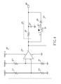
- FIG. 4 illustrates an implementation example of a switching control unit in an electronic device according to an exemplary embodiment of the present invention.
- FIG. 4 corresponds to an exemplary embodiment in which, when a control signal is high, switching is performed such that the power B is supplied to a load, and when the control signal is low, switching is performed such that the power A is supplied to the load.
- the second power determination unit 302 includes a plurality of resistors 411 to 414 and a comparator 416.
- the delay unit 304 includes a resistor 421 and a capacitor 422, and the unidirectional conduction unit 306 includes a transistor 431 and a diode 432.
- the control signal for determining a switching direction is the output signal of the comparator 416, and is determined according to a result of a comparison of the voltage values of signals input to a first terminal and a third terminal of the comparator 416.
- a voltage value of the power A is equal to a voltage value of the power B. Therefore, if the power A and the power B are input as is, a comparison cannot be accomplished. Accordingly, the plurality of resistors 411 to 414 divide the voltage of the power A and the voltage of the power B, thereby generating a voltage difference for comparison.
- the values of the resistors 411 to 414 are selected such that the voltage applied to a third terminal of the comparator 416 is higher than the voltage applied to the first terminal.
- a fifth terminal of the comparator 416 is a power supply terminal for operation of the comparator 416. According to the above-described structure, the comparator 416 outputs a high signal upon generation of the power B, and a low signal upon discontinuing of the power B.
- the delay unit 304 will be described in detail below.
- the delay unit 304 may be configured by a Resistance-Capacitance (RC) circuit.
- the delay unit 304 includes a resistor 421 and a capacitor 422 as shown in FIG. 4 . That is, the delay unit 304 includes a RC filter.
- the specific resistance of the resistor 421 and the specific capacitance of the capacitor 422 may vary according to a specific exemplary embodiment.
- the delay unit 304 may be implemented in a different form from the RC circuit.
- the unidirectional conduction unit 306 includes the transistor 431 and the diode 432.
- the transistor 431 is a p-channel Field Effective Transistor (FET), and operates as a switch.
- FET Field Effective Transistor
- the gate and drain of the transistor 431 are connected to the output terminal of the comparator 416, and the source is connected to a final output terminal 440 through the diode 432. Therefore, when the high signal is output from the comparator 416, a VGS deviates from the operating voltage of the transistor 431, and the transistor 431 operates as an open circuit.
- the VGS becomes the operating voltage of the transistor 431, and the transistor 431 operates as a short circuit. That is, the transistor 431 functions as a switch which is turned on when the low signal is applied thereto.
- the diode 432 is for complementing the operation of the transistor 431. The diode 432 blocks the flow of current in a direction toward the final output terminal 440, and allows only the flow of current in a direction from the final output terminal 440 to the transistor 431. That is, the cathode of the diode 432 is connected to the source of the transistor 431, and the anode of the diode 432 is connected to the final output terminal 440.
- the diode 432 conducts a current only when the source of the transistor 431 is at a higher voltage than the final output terminal 440. Due to the above-described structure, the unidirectional conduction unit 306 is conductive only when the low signal is output from the comparator 416. In FIG. 4 , the unidirectional conduction unit 306 includes both the transistor 431 and the diode 432. However, the unidirectional conduction unit 306 may include any one of the transistor 431 and the diode 432.
- the output of the comparator 416 transits to a low state. Due to this, a voltage difference occurs between the output terminal of the comparator 416 and the final output terminal 440, and a current flowing from the final output terminal 440 to the output terminal of the comparator 416 is generated.
- the transistor 431 operates as a short circuit, and the diode 432 conducts a current. Therefore, the current flows toward both the delay unit 304 and the unidirectional conduction unit 306.
- the delay time by the delay unit 304 has not elapsed, the output of the final output terminal 440 transits to a low state immediately due to a current flowing through the unidirectional conduction unit 306.
- the control signal for performing switching such that the power A is supplied to the load is output immediately after the power B is discontinued.
- FIG. 5 illustrates another implementation example of a switching control unit in an electronic device according to an exemplary embodiment of the present invention.
- FIG. 5 corresponds to an exemplary embodiment in which, when a control signal is high, switching is performed such that the power A is supplied to a load, and when the control signal is low, switching is performed such that the power B is supplied to the load.
- a second power determination unit 302 includes a plurality of resistors 511 to 514 and a comparator 516.
- a delay unit 304 includes a resistor 521 and a capacitor 522, and a unidirectional conduction unit 306 includes a diode 531 and a transistor 532.
- the control signal for determining a switching direction is the output signal of the comparator 516, and the control signal is determined according to a result of a comparison of the voltage values of signals input to the first terminal and to the third terminal of the comparator 516.
- the voltage value of the power A is equal to that of the power B. Therefore, if the power A and the power B are input as they are, a comparison cannot be accomplished. Accordingly, the plurality of resistors 511 to 514 divide the voltages of the power A and the voltage of the power B, causing a voltage difference for comparison.
- the values of the resistors 511 to 514 are selected such that the voltage applied to a third terminal of the comparator 514 is higher than a voltage applied to a first terminal of the comparator 514.
- a fifth terminal of the comparator 516 is a power supply terminal for operation of the comparator 516. According to the above-described structure, the comparator 516 outputs a low signal upon generation of the power B, and a high signal upon discontinuing the power B.
- the delay unit 304 will be described in detail below.
- the delay unit 304 may be configured by a RC circuit.
- the delay unit 304 includes a resistor 521 and a capacitor 522 as in FIG. 5 .
- the delay unit 304 includes a RC filter.
- the specific resistance of the resistor 521 and the specific capacitance of the capacitor 522 may vary according to a specific exemplary embodiment.
- the delay unit 304 may be implemented in a different form from the RC circuit.
- the unidirectional conduction unit 306 includes the diode 531 and the transistor 532.
- the transistor 532 is an n-channel FET, and operates as a switch.
- the gate of the transistor 532 is connected to the output terminal of the comparator 516, the drain thereof is connected through the diode 531 to the output terminal of the comparator 516, and the source thereof is connected to a final output terminal 540. Therefore, when the low signal is output from the comparator 516, a VGS deviates from the operating voltage of the transistor 532, and the transistor 532 operates as an open circuit.
- the VGS becomes the operating voltage of the transistor 532, and the transistor 532 operates as a short circuit. That is, the transistor 532 functions as a switch which is turned on when the high signal is applied thereto.
- the diode 531 is for complementing the operation of the transistor 532. The diode 516 blocks the flow of current in a direction from the final output terminal 540 to the transistor 532, and allows only the flow of current in a direction from the output terminal of the comparator 516 to the final output terminal 540.
- the cathode of the diode 531 is connected to the drain of the transistor 532, and the anode of the diode 531 is connected to the output terminal of the comparator 516. Therefore, the diode 531 conducts a current only when the final output terminal 540 is at a higher voltage than the drain of the transistor 532. Due to the above-described structure, the unidirectional conduction unit 306 is conductive only when the high signal is output from the comparator 516. In FIG. 5 , the unidirectional conduction unit 306 includes both the transistor 531 and the diode 532. However, the unidirectional conduction unit 306 may include any one of the diode 531 and the transistor 532.
- the output of the final output terminal 540 transits to a low state only after the delay time by the delay unit 304 has elapsed.
- the control signal for performing switching such that the power B is supplied to the load is output after delay of the predetermined time.
- the output of the comparator 516 transits to a high state. Due to this, a voltage difference occurs between the output terminal of the comparator 516 and the final output terminal 540, and a current flowing from the final output terminal 540 to the output terminal of the comparator 516 is generated.
- the transistor 532 operates as a short circuit, and the diode 531 conducts a current. Therefore, the current flows toward both the delay unit 304 and the unidirectional conduction unit 306.
- the delay time by the delay unit 304 has not elapsed, the output of the final output terminal 540 transits to a high state immediately due to a current flowing through the unidirectional conduction unit 306.
- the control signal for performing switching such that the power A is supplied to the load is output immediately after the power B is discontinued.
- FIG. 6 illustrates a block configuration of an electronic device according to an exemplary embodiment of the present invention.
- FIG. 6 illustrates a block configuration of a portable communication device in a case where a power supply mechanism according to an exemplary embodiment of the present invention is applied to the portable communication device.
- the electronic device includes a control unit 610, a display unit 620, an input unit 630, a memory 640, a communication unit 650, a power supply unit 660, a battery 670 and a TA connection unit 680.
- the control unit 610 controls an overall operation of the electronic device, and includes at least one processor, for example, an application processor.
- the display unit 620 is a unit for visually transmitting information to a user, and may include at least one of a Liquid Crystal Display (LCD), a Light Emitting Diode (LED), a Light emitting Polymer Display (LPD), an Organic Light Emitting Diode (OLED), an Active Matrix Organic Light Emitting Diode (AMOLED) and a Flexible LED (FLED).
- LCD Liquid Crystal Display
- LED Light Emitting Diode
- LPD Light emitting Polymer Display
- OLED Organic Light Emitting Diode
- AMOLED Active Matrix Organic Light Emitting Diode
- FLED Flexible LED
- the input unit 630 is a unit for processing input from the user, and may include a keypad, a touchscreen or the like.
- the memory 640 is a storage unit for storing an operation program, an application, setting information, user contents and the like.
- the communication unit 650 is a unit for providing an interface for communication with the outside, and includes a modem, a Radio Frequency (RF) processing block, an antenna, and the like.
- RF Radio Frequency
- the power supply unit 660 is a unit for supplying required power to the control unit 610, the display unit 620, the input unit 630, the memory 640, and the communication unit 650.
- the power supply unit 660 selectively supplies power generated from the battery 670 and power generated from the TA connected to the TA connection unit 680 to the above-described blocks.
- the power supply unit 660 may include a power switching unit 662 for switching power and a switching control unit 664 for controlling the switching operation of the power switching unit 664.
- the switching control unit 664 may be configured as illustrated in FIG. 3 .
- the present invention may be implemented in an electronic device including a portable terminal such as, for example, a smart phone and a mobile telecommunication terminal.
- a portable terminal such as, for example, a smart phone and a mobile telecommunication terminal.
- a portable terminal is used as an example for the electronic device.
- FIG. 7 illustrates an operation process of an electronic device according to an exemplary embodiment of the present invention.
- the electronic device determines whether second power is generated.
- the second power is power that is discontinuously supplied to the electronic device. That is, the process illustrated in FIG. 7 is under the assumption that basic power is continuously supplied to the electronic device.
- the basic power may include power from the battery, and the second power may include power supplied from the outside upon connection of the TA.
- the electronic device When the second power is generated, in operation 703, the electronic device performs power switching after delay of a predetermined time. That is, the electronic device performs switching such that the electronic device uses the second power during usage of the basic power. In this case, the electronic device performs switching to the second power after the second power has been generated and the predetermined time has elapsed.
- the power supply device provides the control signal for the switching to the switch through the delay circuit.
- the delay time circuit may include an RC filter.
- the electronic device checks whether the second power is discontinued or cut-off.
- the second power may be discontinued during the operation of the electronic device. For example, in a case where the second power is supplied through the TA, the second power may be discontinued when the TA is separated from the electronic device. When the second power is discontinued, only the basic power exists.
- the electronic device When the second power is discontinued, in operation 707, the electronic device performs power switching without time delay. That is, the electronic device performs switching such that the electronic device uses the basic power during the use of the second power. In this case, the electronic device performs switching to the basic power immediately after the second power is discontinued. For this, the power supply device provides the control signal for the switching to the switch through a unidirectional path connected in parallel to the delay circuit.
- FIGS. 8A and 8B illustrate a performance of a power supply mechanism according to an exemplary embodiment of the present invention.
- FIGS. 8A and 8B illustrate a change in power according to power switching when a second power is generated.
- FIG. 8A is a graph in a case where the power supply mechanism according to an exemplary embodiment of the present invention is not applied
- FIG. 8B is a graph in a case where the power supply mechanism according to an exemplary embodiment of the present invention is applied.
- FIG. 8A since power switching is performed without a delay of the predetermined time when the second power is generated, the temporary drop of power occurs in an interval A 810.
- FIG. 8B since power switching is performed after delay of the predetermined time when the second power is generated, power is prevented from being unstable after the second power has been stabilized prior to the switching.
- Any such software may be stored in a non-transitory computer readable storage medium.
- the non-transitory computer readable storage medium stores one or more programs (software modules), the one or more programs comprising instructions, which when executed by one or more processors in an electronic device, cause the electronic device to perform a method of the present disclosure.
- Any such software may be stored in the form of volatile or non-volatile storage such as, for example, a storage device like a Read Only Memory (ROM), whether erasable or rewritable or not, or in the form of memory such as, for example, Random Access Memory (RAM), memory chips, device or integrated circuits or on an optically or magnetically readable medium such as, for example, a Compact Disk (CD), Digital Versatile Disc (DVD), magnetic disk or magnetic tape or the like.
- ROM Read Only Memory
- RAM Random Access Memory
- CD Compact Disk
- DVD Digital Versatile Disc
- the storage devices and storage media are various embodiments of non-transitory machine-readable storage that are suitable for storing a program or programs comprising instructions that, when executed, implement various embodiments of the present disclosure. Accordingly, various embodiments provide a program comprising code for implementing apparatus or a method as claimed in any one of the claims of this specification and a non-transitory machine-readable storage storing such a program.
Landscapes
- Engineering & Computer Science (AREA)
- Power Engineering (AREA)
- Theoretical Computer Science (AREA)
- Physics & Mathematics (AREA)
- General Engineering & Computer Science (AREA)
- General Physics & Mathematics (AREA)
- Charge And Discharge Circuits For Batteries Or The Like (AREA)
- Direct Current Feeding And Distribution (AREA)
- Dc-Dc Converters (AREA)
Applications Claiming Priority (1)
| Application Number | Priority Date | Filing Date | Title |
|---|---|---|---|
| KR20120094661A KR20140028427A (ko) | 2012-08-29 | 2012-08-29 | 전자 장치에서 다수 전원들 간 전환 장치 및 방법 |
Publications (2)
| Publication Number | Publication Date |
|---|---|
| EP2703943A2 true EP2703943A2 (fr) | 2014-03-05 |
| EP2703943A3 EP2703943A3 (fr) | 2015-09-30 |
Family
ID=49123645
Family Applications (1)
| Application Number | Title | Priority Date | Filing Date |
|---|---|---|---|
| EP13182026.8A Withdrawn EP2703943A3 (fr) | 2012-08-29 | 2013-08-28 | Appareil et procédé permettant de changer d'alimentation dans un dispositif électronique |
Country Status (4)
| Country | Link |
|---|---|
| US (1) | US20140062208A1 (fr) |
| EP (1) | EP2703943A3 (fr) |
| KR (1) | KR20140028427A (fr) |
| CN (1) | CN103683471A (fr) |
Cited By (1)
| Publication number | Priority date | Publication date | Assignee | Title |
|---|---|---|---|---|
| WO2017212448A1 (fr) * | 2016-06-09 | 2017-12-14 | Neill Human | Système d'alimentation électrique pour un élément résistif alimenté électriquement |
Families Citing this family (6)
| Publication number | Priority date | Publication date | Assignee | Title |
|---|---|---|---|---|
| CN106033242B (zh) * | 2015-03-09 | 2019-08-16 | 光宝电子(广州)有限公司 | 外部电源供应器以及应用于其的系统连接侦测单元 |
| KR101758463B1 (ko) | 2015-09-10 | 2017-07-14 | 허영회 | 자전거용 발전기 및 이러한 발전기에 착탈 가능한 배터리모듈 |
| US10913506B2 (en) | 2015-03-09 | 2021-02-09 | Young Hui HUR | Generator for bicycle, and battery module attachable/detachable to/from generator |
| KR101825714B1 (ko) | 2015-06-25 | 2018-02-06 | 허영회 | 발전기용 회전자 |
| TWI637580B (zh) * | 2016-01-11 | 2018-10-01 | 台達電子工業股份有限公司 | 轉換器與其控制方法 |
| CN106227318A (zh) * | 2016-08-23 | 2016-12-14 | 浪潮电子信息产业股份有限公司 | 一种控制电路转换的装置及系统 |
Family Cites Families (6)
| Publication number | Priority date | Publication date | Assignee | Title |
|---|---|---|---|---|
| US6854065B2 (en) * | 2001-07-30 | 2005-02-08 | Hewlett-Packard Development Company, L.P. | Loadshedding uninterruptible power supply |
| CN100459369C (zh) * | 2006-05-29 | 2009-02-04 | 华为技术有限公司 | 一种主备电源的切换控制装置 |
| CN101436830B (zh) * | 2007-11-15 | 2011-06-08 | 鸿富锦精密工业(深圳)有限公司 | 电源装置及其保护方法 |
| CN201302072Y (zh) * | 2008-11-26 | 2009-09-02 | 苏州市相城区富顿厚膜电路制造厂 | 带转换继电电路的太阳能路灯 |
| TWI405408B (zh) * | 2009-04-14 | 2013-08-11 | Novatek Microelectronics Corp | 可連續提供電源之切換控制方法及其相關裝置與電源供應系統 |
| CN102298884A (zh) * | 2011-08-28 | 2011-12-28 | 长沙理工大学 | 智能型太阳能广告牌 |
-
2012
- 2012-08-29 KR KR20120094661A patent/KR20140028427A/ko not_active Application Discontinuation
-
2013
- 2013-08-27 US US14/011,163 patent/US20140062208A1/en not_active Abandoned
- 2013-08-28 EP EP13182026.8A patent/EP2703943A3/fr not_active Withdrawn
- 2013-08-28 CN CN201310381640.7A patent/CN103683471A/zh active Pending
Non-Patent Citations (1)
| Title |
|---|
| None |
Cited By (1)
| Publication number | Priority date | Publication date | Assignee | Title |
|---|---|---|---|---|
| WO2017212448A1 (fr) * | 2016-06-09 | 2017-12-14 | Neill Human | Système d'alimentation électrique pour un élément résistif alimenté électriquement |
Also Published As
| Publication number | Publication date |
|---|---|
| US20140062208A1 (en) | 2014-03-06 |
| KR20140028427A (ko) | 2014-03-10 |
| CN103683471A (zh) | 2014-03-26 |
| EP2703943A3 (fr) | 2015-09-30 |
Similar Documents
| Publication | Publication Date | Title |
|---|---|---|
| EP2703943A2 (fr) | Appareil et procédé permettant de changer d'alimentation dans un dispositif électronique | |
| US9882480B2 (en) | Voltage converter for controlling a voltage of a flying capacitor and a voltage control method thereof | |
| TWI769160B (zh) | 用以軟啟動大功率電荷泵的方法、電路,及電子系統 | |
| US8866341B2 (en) | Voltage regulator | |
| JP6657478B2 (ja) | 供給電圧を安定させるためのデバイスおよび方法 | |
| US20170083034A1 (en) | Voltage regulator using a multi-power and gain-boosting technique and mobile devices including the same | |
| US20120098508A1 (en) | Voltage regulator having soft starting function and method of controlling the same | |
| US9577505B1 (en) | Bootstrap controller for switching power supply | |
| KR20120042649A (ko) | 소프트 스타팅 기능을 갖는 전압 레귤레이터 및 전압 레귤레이터의 제어 방법 | |
| US20160033982A1 (en) | Dc-dc converting circuit and a power management chip package including the same | |
| US10559968B2 (en) | Charge/discharge control circuit and battery apparatus | |
| JP2015211541A (ja) | 充電回路、パワーマネージメント回路、およびそれを用いた電子機器 | |
| US10305305B2 (en) | Unified high power and low power battery charger | |
| CN107070444B (zh) | 具有细粒度功率门控的非易失性铁电逻辑 | |
| US10261116B2 (en) | Apparatus for performing resistance control on a current sensing component in an electronic device, and associated method | |
| TWI462430B (zh) | 電源管理系統 | |
| US9791916B2 (en) | Control circuit including load switch, electronic apparatus including the load switch, and control method thereof | |
| JP2006228027A (ja) | 電源装置及び電源制御方法 | |
| US20130057324A1 (en) | Circuit for clearing complementary metal oxide semiconductor information | |
| JP6446181B2 (ja) | 充電回路およびそれを利用した電子機器 | |
| US20150188348A1 (en) | Power supply circuit and electronic device | |
| US20100007400A1 (en) | Power supply circuit for pulse width modulation controller | |
| US9443431B1 (en) | System and method for preventing undesirable substantially concurrent switching in multiple power circuits | |
| JP5310794B2 (ja) | 低リーク電圧検出回路 | |
| US10630075B2 (en) | Multi-level output circuit having centralized ESD protection |
Legal Events
| Date | Code | Title | Description |
|---|---|---|---|
| 17P | Request for examination filed |
Effective date: 20130828 |
|
| AK | Designated contracting states |
Kind code of ref document: A2 Designated state(s): AL AT BE BG CH CY CZ DE DK EE ES FI FR GB GR HR HU IE IS IT LI LT LU LV MC MK MT NL NO PL PT RO RS SE SI SK SM TR |
|
| AX | Request for extension of the european patent |
Extension state: BA ME |
|
| PUAI | Public reference made under article 153(3) epc to a published international application that has entered the european phase |
Free format text: ORIGINAL CODE: 0009012 |
|
| PUAL | Search report despatched |
Free format text: ORIGINAL CODE: 0009013 |
|
| AK | Designated contracting states |
Kind code of ref document: A3 Designated state(s): AL AT BE BG CH CY CZ DE DK EE ES FI FR GB GR HR HU IE IS IT LI LT LU LV MC MK MT NL NO PL PT RO RS SE SI SK SM TR |
|
| AX | Request for extension of the european patent |
Extension state: BA ME |
|
| RIC1 | Information provided on ipc code assigned before grant |
Ipc: H02J 7/34 20060101ALI20150824BHEP Ipc: G06F 1/26 20060101AFI20150824BHEP |
|
| 17Q | First examination report despatched |
Effective date: 20160818 |
|
| STAA | Information on the status of an ep patent application or granted ep patent |
Free format text: STATUS: THE APPLICATION IS DEEMED TO BE WITHDRAWN |
|
| 18D | Application deemed to be withdrawn |
Effective date: 20170103 |