EP2701040A2 - Capacitive in-cell touch panel and display device - Google Patents
Capacitive in-cell touch panel and display device Download PDFInfo
- Publication number
- EP2701040A2 EP2701040A2 EP13181149.9A EP13181149A EP2701040A2 EP 2701040 A2 EP2701040 A2 EP 2701040A2 EP 13181149 A EP13181149 A EP 13181149A EP 2701040 A2 EP2701040 A2 EP 2701040A2
- Authority
- EP
- European Patent Office
- Prior art keywords
- touch
- electrodes
- disposed
- electrode
- touch panel
- Prior art date
- Legal status (The legal status is an assumption and is not a legal conclusion. Google has not performed a legal analysis and makes no representation as to the accuracy of the status listed.)
- Withdrawn
Links
Images


Classifications
-
- G—PHYSICS
- G02—OPTICS
- G02F—OPTICAL DEVICES OR ARRANGEMENTS FOR THE CONTROL OF LIGHT BY MODIFICATION OF THE OPTICAL PROPERTIES OF THE MEDIA OF THE ELEMENTS INVOLVED THEREIN; NON-LINEAR OPTICS; FREQUENCY-CHANGING OF LIGHT; OPTICAL LOGIC ELEMENTS; OPTICAL ANALOGUE/DIGITAL CONVERTERS
- G02F1/00—Devices or arrangements for the control of the intensity, colour, phase, polarisation or direction of light arriving from an independent light source, e.g. switching, gating or modulating; Non-linear optics
- G02F1/01—Devices or arrangements for the control of the intensity, colour, phase, polarisation or direction of light arriving from an independent light source, e.g. switching, gating or modulating; Non-linear optics for the control of the intensity, phase, polarisation or colour
- G02F1/13—Devices or arrangements for the control of the intensity, colour, phase, polarisation or direction of light arriving from an independent light source, e.g. switching, gating or modulating; Non-linear optics for the control of the intensity, phase, polarisation or colour based on liquid crystals, e.g. single liquid crystal display cells
- G02F1/133—Constructional arrangements; Operation of liquid crystal cells; Circuit arrangements
- G02F1/1333—Constructional arrangements; Manufacturing methods
- G02F1/13338—Input devices, e.g. touch panels
-
- G—PHYSICS
- G06—COMPUTING OR CALCULATING; COUNTING
- G06F—ELECTRIC DIGITAL DATA PROCESSING
- G06F3/00—Input arrangements for transferring data to be processed into a form capable of being handled by the computer; Output arrangements for transferring data from processing unit to output unit, e.g. interface arrangements
- G06F3/01—Input arrangements or combined input and output arrangements for interaction between user and computer
- G06F3/03—Arrangements for converting the position or the displacement of a member into a coded form
- G06F3/041—Digitisers, e.g. for touch screens or touch pads, characterised by the transducing means
- G06F3/0412—Digitisers structurally integrated in a display
-
- G—PHYSICS
- G06—COMPUTING OR CALCULATING; COUNTING
- G06F—ELECTRIC DIGITAL DATA PROCESSING
- G06F3/00—Input arrangements for transferring data to be processed into a form capable of being handled by the computer; Output arrangements for transferring data from processing unit to output unit, e.g. interface arrangements
- G06F3/01—Input arrangements or combined input and output arrangements for interaction between user and computer
- G06F3/03—Arrangements for converting the position or the displacement of a member into a coded form
- G06F3/041—Digitisers, e.g. for touch screens or touch pads, characterised by the transducing means
- G06F3/044—Digitisers, e.g. for touch screens or touch pads, characterised by the transducing means by capacitive means
- G06F3/0443—Digitisers, e.g. for touch screens or touch pads, characterised by the transducing means by capacitive means using a single layer of sensing electrodes
-
- G—PHYSICS
- G06—COMPUTING OR CALCULATING; COUNTING
- G06F—ELECTRIC DIGITAL DATA PROCESSING
- G06F3/00—Input arrangements for transferring data to be processed into a form capable of being handled by the computer; Output arrangements for transferring data from processing unit to output unit, e.g. interface arrangements
- G06F3/01—Input arrangements or combined input and output arrangements for interaction between user and computer
- G06F3/03—Arrangements for converting the position or the displacement of a member into a coded form
- G06F3/041—Digitisers, e.g. for touch screens or touch pads, characterised by the transducing means
- G06F3/044—Digitisers, e.g. for touch screens or touch pads, characterised by the transducing means by capacitive means
- G06F3/0446—Digitisers, e.g. for touch screens or touch pads, characterised by the transducing means by capacitive means using a grid-like structure of electrodes in at least two directions, e.g. using row and column electrodes
Definitions
- Embodiments of the invention relate to a capacitive in-cell touch panel and a display device.
- touch panel may be classified into an add on mode touch panel, an on cell touch panel and an in-cell touch panel, based on the structural configuration of the touch panels.
- the add on mode touch panel employs a touch panel and a liquid crystal display (LCD) which are separately fabricated and then bonded together to form a LCD with a touch function.
- LCD liquid crystal display
- Such an add-on mode touch panel suffers from the disadvantages of high production cost, low transmitivity and thick module.
- An in-cell touch panel embeds touch electrodes of the touch panel inside the LCD, which not only reduces the overall thickness of the module, but also significantly reduces the production cost of the touch panel. As a result, the in-cell touch panel is very popular with panel manufactures.
- the currently available capacitive in-cell touch panel is implemented by directly adding a touch scan line and a touch sense line on a conventional Thin Film Transistor (TFT) array substrate. That is, two layers of strip-shape Indium Tin Oxides (ITO) electrodes intersecting each other in different planes are formed on a surface of the TFT array substrate. The two layers of ITO electrodes respectively function as the touch drive line and the touch sense line of the touch panel and an induction capacitor is generated at the non-coplanar intersection of the two ITO electrodes.
- the functioning procedure of the in-cell touch panel is as follows: when a touch drive signal is applied to the ITO electrode that functions as the touch drive line, a voltage signal coupled through the induction capacitor from the touch sense line is detected.
- the above in-cell touch panel structure requires two separate drive chips ICs to realize touch driving and display driving respectively and therefore has a high cost.
- Embodiments of the invention provide a capacitive in-cell touch panel and a display device so as to provide a capacitive in-cell touch panel with a relatively low cost.
- An embodiment of the invention provides a capacitive in-cell touch panel, comprising: a color film substrate, a thin film transistor (TFT) array substrate, and a liquid crystal layer disposed between the color film substrate and the TFT array substrate, a plurality of pixel units arranged in a matrix are disposed on the TFT array substrate.
- TFT thin film transistor
- the capacitive in-cell touch panel further comprises: at least one touch drive electrodes disposed on a side of the TFT array substrate facing the liquid crystal layer, and at least one touch sense electrode disposed on a side of the color film substrate facing the liquid crystal layer, wherein, wiring of the touch sense electrode runs along a column direction of the pixel units, wiring of the touch drive electrode runs along a row direction of the pixel units and the touch drive electrode is electrically connected to at least one gate line of the TFT array substrate.
- Each touch drive electrode comprises a plurality of touch drive sub-electrodes arranged in the same row, the touch drive sub-electrodes are disposed between adjacent columns of pixel units.
- Another embodiment of the invention provides a display device comprising the capacitive in-cell touch panel provided by the embodiment of the invention.
- the capacitive in-cell touch panel and the display device provided by the embodiments of the invention have at least one touch sense electrode disposed on the color film substrate and at least one touch drive electrode disposed on the TFT array substrate.
- the touch drive electrode is electrically connected to the gate line in the TFT array substrate, wherein each touch drive electrode is made up of touch drive sub-electrodes disposed in the same row and between adjacent columns of pixel units.
- the capacitive in-cell touch panel and the display device provided by the embodiments of the invention employ the input display signal of the gate line electrically connected to the touch drive electrode as a drive signal of the touch to realize the touch control function, thereby avoiding the addition of the IC for touch drive and reducing the production cost.
- Fig. 1 schematically illustrates a configuration of a capacitive in-cell touch panel in accordance with an embodiment of the invention
- Fig. 2 schematically illustrates a configuration of a TFT array substrate of the touch panel in accordance with an embodiment of the invention
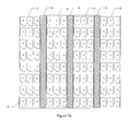
- Figs. 3a ⁇ 3c schematically illustrate a configuration of a color film substrate of the touch panel in accordance with an embodiment of the invention
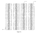
- Figs. 4a ⁇ 4b schematically illustrate a configuration of a cell-assembled color film substrate and TFT array substrate of the touch panel in accordance with an embodiment of the invention
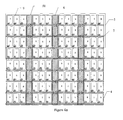
- Figs. 5a ⁇ 5c schematically illustrate a projected electric field of the touch panel in accordance with an embodiment of the invention.
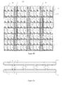
- Fig. 6 schematically illustrates a connection relation of the touch sense line in accordance with an embodiment of the invention.
- connection are not intended to define a physical connection or mechanical connection, but may include an electrical connection, directly or indirectly.
- "On,” “under,” “right,” “left” and the like are only used to indicate relative position relationship, and when the position of the object which is described is changed, the relative position relationship may be changed accordingly.
- each film layer in the drawings are just for illustrative purpose and do not represent the real proportion of the TFT array substrate and the color film substrate.
- a capacitive in-cell touch panel provided by an embodiment of the invention is illustrated in Fig. 1 .
- the capacitive in-cell touch panel comprises: a color film substrate 1, a TFT array substrate 2 and a liquid crystal layer 3 disposed between the color film substrate 1 and the TFT array substrate 2.
- a plurality of pixel units 4 arranged into a matrix is disposed on the TFT array substrate 2.
- the capacitive in-cell touch panel further comprises: at least one touch drive electrode 5 disposed on a side of the TFT array substrate 2 facing the liquid crystal layer 3, and at least one touch sense electrode 6 disposed on a side of the color film substrate 1 facing the liquid crystal layer 3, wherein wiring of the touch sense electrode 6 runs along a column direction of the pixel units 4.
- Fig. 2 illustrates a top plan view of the TFT array substrate. It can be seen from Fig. 2 that a pixel element 4 comprises three sub-pixel units R, G, B, and wiring of the touch drive electrode 5 runs along a row direction of the pixel units 4 and the touch drive electrode 5 is electrically connected to at least one gate line 7 of the TFT array substrate 2.
- Each touch drive electrode 5 comprises a plurality of touch drive sub-electrodes 51 arranged in the same row, and the touch drive sub-electrodes 51 are disposed between adjacent columns of pixel units 4.
- the aforementioned capacitive in-cell touch panel as provided by the embodiment of the invention employs a display signal of the gate line electrically connected to the touch drive electrode as a touch drive signal to realize the touch control function, thereby avoiding the addition of an IC for touch drive, which accordingly saves the fabrication cost.
- the touch drive sub-electrodes may be disposed in the same layer as a source electrode as well as a drain electrode of the TFT array substrate, that is, a pattern of the source electrode and the drain electrode of the TFT and a pattern of the touch drive sub-electrodes are fabricated in a single patterning process. Therefore, no additional patterning process will be introduced to the fabrication of the TFT array substrate and the fabrication cost of the TFT array substrate as the touch panel will not be increased.
- touch drive sub-electrodes in the same touch drive electrode may be electrically connected with each other by a drive data line disposed in the same layer as the touch drive electrode.
- the drive data line is disposed between adjacent rows of pixel units and electrically connected to the gate line. That is, the drive data line and each of the touch drive sub-electrodes connected thereto are fabricated at the same time.
- the drive data line may be disposed parallel to the gate line of the TFT array substrate, that is, disposed in a gap between adjacent rows of pixel unit. Then, the between the drive data line is electrically connected to the gate line using a via hole such that the gate line may provide signal to the drive data line.
- each touch drive sub-electrode 51 in the same touch drive electrode 5 may be electrically connected to the gate line 7 directly, such that a patterning process for fabricating the drive data line may be omitted.
- the touch drive sub-electrode 51 is directly connected to an overlapped gate line 7 using a via hole; while a wire connection is used when the touch drive sub-electrode 51 does not overlap with the gate line 7.
- the touch drive sub-electrodes in each touch drive electrode are disposed in the gap between pixel units, the touch drive sub-electrode will not have a width greater than the gap between adjacent columns of pixel units.
- the touch panel has a precision in the order of a millimeter, while the LCD has a precision of a micrometer.
- the precision of the touch panel is dependent on the length of the touch drive sub-electrodes, that is, the length of the touch drive sub-electrodes may be selected according to the required touch precision. Therefore, the length of each touch drive sub-electrode will span across the length of a number of pixel units in the column direction and normally is above 2mm.
- each touch drive sub-electrode will overlap with a plurality of gate lines in the TFT array substrate providing the display signal for the TFT, and a parasitic capacitance will be generated at the overlapping part. The larger the overlapping part is, the larger the parasitic capacitor is.
- the parasitic capacitor may cause defections such as greenish picture and residual lines which will become more apparent with the increase of the panel size.
- each touch drive sub-electrode 51 may be formed as a plurality of electrically connected drive dot electrodes adjacent each other in the column direction as illustrated in Fig. 2 .
- the drive dot electrodes are disposed between adjacent pixel units and connected to each other via wires.
- Fig. 2 an example of a touch drive sub-electrode 51 having four drive dot electrodes is illustrated, and the broken line marks such a dot drive electrode.
- the touch sense electrode on the color film substrate may be disposed between a substrate and a color resin of the color film substrate, or on a side of the color resin of the color film substrate facing the liquid crystal layer.
- the color film unit on the color film substrate, which has a one-to-one correspondence with the pixel units on the TFT array substrate, and the color film unit comprises three color film sub-elements R, G, B. Since the wiring of the touch sense electrode runs along the column direction of the pixel units, the projection of the touch sense electrode on the TFT array substrate may at least partially cover the touch drive electrode. Moreover, the plurality of touch drive sub-electrodes arranged in the same row included in each touch drive electrode is disposed between adjacent columns of pixel units. When implemented, for example, all touch sense electrodes 6 may be disposed between adjacent columns of color filter elements 8 on the color film substrate, as illustrated in Fig. 3a .
- the projection of the touch sense electrodes 6 on the TFT array substrate overlays all of the touch drive electrode as illustrated in Fig. 4a .
- the touch sense electrode 6 can be selectively disposed between some of the adjacent columns of color film elements 8. As an example, a touch sense electrode 6 is disposed at every other gap, the gaps are between adjacent columns of color filter elements 8 as illustrated in Fig. 3b .
- the projection of the touch sense electrode 6 on the TFT array substrate is illustrated in Fig. 4b , which partially covers the touch drive electrode and will not be described in detail here.
- shield electrodes fabricated on a side of the color film substrate opposite to the liquid crystal layer in conventional technologies may be fabricated on the side of the color film substrate facing the liquid crystal layer, which may facilitate the thinning process after cell assembling the color film substrate and the TFT array substrate.
- a particular liquid is used to etch the exposed substrate.
- a plurality of shield electrodes may be disposed between the substrate and the color resin of the color film substrate or on the side of the color resin of the color film substrate facing the liquid crystal layer.
- a common electrode electrically connected to the shield electrodes may be used to supply a common electrode signal to the shield electrodes so as to shield interference from external signals.
- fabricating the shield electrodes between the substrate and the color resin of the color film substrate can help shielding the interference from the external signals in a better way.
- the shield electrodes fabricated as a whole layer in conventional technologies is fabricated as a strip, and wirings of the shield electrodes and touch sense electrode run in the same direction, thus projections of them on the color film substrate do not overlap with each other.
- the projection of a shield electrode on the TFT array substrate covers all of a column of pixel units.
- a shield electrode 9 on the color film substrate covers a column of color filter element 8 comprising R, G and B.
- the shield electrode 9 and the touch sense electrode 6 may be disposed in the same layer as there is no overlap between the patterns of the shield electrode 9 and the touch sense electrode 6.
- the shield electrodes and the touch sense electrodes may be disposed in different layers of the color film substrate, which will not be limited here.
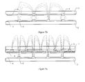
- Fig. 4a a top plan view after cell assembling the color film substrate and the TFT array substrate is illustrated in Fig. 4a .
- the touch sense line 6 substantially overlays the touch drive sub-electrode 51, which is not advantageous for the the electric field from the touch drive electrode projected through the gap between the shield electrodes 9 as illustrated in Fig. 5a .
- Fig. 4b a top view after cell assembling the color film substrate and the TFT array substrate is illustrated in Fig. 4b . It is seen from Fig.
- the touch sense line 6 partially overlays the touch drive sub-electrode 51, that is, a part of the touch drive sub-electrodes 51 is not blocked by the touch sense electrodes 6. Therefore, the electric field from the touch drive electrode 5 can be partially projected to the touch sense electrode 6 through the gap between the shield electrodes 9 as illustrated in Fig. 5b .
- each touch sense electrode can also be disposed such that the projection on the TFT array substrate does not overlay the touch drive electrode.
- the touch sense electrode 6 overlays a column of color filter sub-elements of the color filter elements.
- the touch sense electrodes 6 are generally disposed between the substrate and the color resin of the color film substrate.
- the color film substrate may further comprises: a plurality of shield electrodes 9 disposed on the side of the color resin of the color film substrate facing the liquid crystal layer, the projection of each shield electrode on the color film substrate at least overlays a touch sense electrode.
- the projection of a shield electrode on the TFT array substrate completely overlays a column of pixel units as illustrated in Fig. 5c .
- the shield electrodes are generally disposed on the side of the color resin of the color film substrate facing the liquid crystal layer.
- a design having the projection of each touch sense electrode on the TFT array substrate overlaying a column of sub-pixel units of a column of pixel units as illustrated in Fig. 5c may further reduce the blockage on the projected electric field. That is, the touch sense electrode 6 is disposed on a column of color filter sub-elements. The electric field from the touch drive electrode 5 may be projected onto the touch sense electrodes 6 through the gap between the shield electrodes 9, without being blocked.
- the color film substrate having the above structure has two layers of electrodes, that is, the shield electrodes 9 and the touch sense electrodes 6.
- thickness of the two electrodes layers are normally above 1000 ⁇ .
- a width of the touch sense electrode is designed as being narrow as possible, e.g. about 20 ⁇ m.
- a specific width value for the touch sense electrode may be determined according to the size, the aperture ratio and the required touch precision of the LCD, which will not be elaborated here.
- a number of adjacent touch sense electrodes may be used as one touch sense electrode.
- several adjacent touch sense lines may be connected conductively using a wire at one end, based on the required touch precision, and work as a single touch sense electrode. As illustrated in Fig.
- an embodiment of the invention further provides a display device comprising the afore-mentioned capacitive in-cell touch panel provided by the embodiment of the invention.
- a display device comprising the afore-mentioned capacitive in-cell touch panel provided by the embodiment of the invention.
- the display device please refer to the embodiments of the above capacitive in-cell touch panel, which will not be described in detail here.
- the capacitive in-cell touch panel and the display device provided by the embodiments of the invention have at least one touch sense electrode disposed on the color film substrate and at least one touch drive electrode disposed on the TFT array substrate, the touch drive electrode is electrically connected to the gate line in the TFT array substrate, wherein each touch drive electrode comprises touch drive sub-electrodes disposed in the same row and between adjacent column of pixel units.
- the capacitive in-cell touch panel and the display device provided by the embodiments of the invention employ the input display signal of the gate line connected to the touch drive electrode as the touch drive signal to realized the touch control function, thereby avoiding the addition of the IC for touch drive and reducing the production cost.
Landscapes
- Engineering & Computer Science (AREA)
- Physics & Mathematics (AREA)
- General Engineering & Computer Science (AREA)
- Theoretical Computer Science (AREA)
- General Physics & Mathematics (AREA)
- Human Computer Interaction (AREA)
- Nonlinear Science (AREA)
- Chemical & Material Sciences (AREA)
- Crystallography & Structural Chemistry (AREA)
- Mathematical Physics (AREA)
- Optics & Photonics (AREA)
- Liquid Crystal (AREA)
- Liquid Crystal Display Device Control (AREA)
- Control Of Indicators Other Than Cathode Ray Tubes (AREA)
- Devices For Indicating Variable Information By Combining Individual Elements (AREA)
Abstract
Description
- Embodiments of the invention relate to a capacitive in-cell touch panel and a display device.
- With the rapid development of display technologies, touch screen panels have been widely-used in people's daily life. Currently, touch panels may be classified into an add on mode touch panel, an on cell touch panel and an in-cell touch panel, based on the structural configuration of the touch panels. Among the various touch panels, the add on mode touch panel employs a touch panel and a liquid crystal display (LCD) which are separately fabricated and then bonded together to form a LCD with a touch function. Such an add-on mode touch panel suffers from the disadvantages of high production cost, low transmitivity and thick module. In contrast. An in-cell touch panel embeds touch electrodes of the touch panel inside the LCD, which not only reduces the overall thickness of the module, but also significantly reduces the production cost of the touch panel. As a result, the in-cell touch panel is very popular with panel manufactures.
- The currently available capacitive in-cell touch panel is implemented by directly adding a touch scan line and a touch sense line on a conventional Thin Film Transistor (TFT) array substrate. That is, two layers of strip-shape Indium Tin Oxides (ITO) electrodes intersecting each other in different planes are formed on a surface of the TFT array substrate. The two layers of ITO electrodes respectively function as the touch drive line and the touch sense line of the touch panel and an induction capacitor is generated at the non-coplanar intersection of the two ITO electrodes. The functioning procedure of the in-cell touch panel is as follows: when a touch drive signal is applied to the ITO electrode that functions as the touch drive line, a voltage signal coupled through the induction capacitor from the touch sense line is detected. During the procedure, when a human body contacts the touch panel, an electric field of the human body will affect the induction capacitor and thereby change the capacitance of the induction capacitor, which in turn changes the voltage signal coupled from the touch sense line. A position of the touch point is then determined from the change of the voltage signal.
- The above in-cell touch panel structure requires two separate drive chips ICs to realize touch driving and display driving respectively and therefore has a high cost.
- Embodiments of the invention provide a capacitive in-cell touch panel and a display device so as to provide a capacitive in-cell touch panel with a relatively low cost.
- An embodiment of the invention provides a capacitive in-cell touch panel, comprising: a color film substrate, a thin film transistor (TFT) array substrate, and a liquid crystal layer disposed between the color film substrate and the TFT array substrate, a plurality of pixel units arranged in a matrix are disposed on the TFT array substrate. The capacitive in-cell touch panel further comprises: at least one touch drive electrodes disposed on a side of the TFT array substrate facing the liquid crystal layer, and at least one touch sense electrode disposed on a side of the color film substrate facing the liquid crystal layer, wherein, wiring of the touch sense electrode runs along a column direction of the pixel units, wiring of the touch drive electrode runs along a row direction of the pixel units and the touch drive electrode is electrically connected to at least one gate line of the TFT array substrate.
- Each touch drive electrode comprises a plurality of touch drive sub-electrodes arranged in the same row, the touch drive sub-electrodes are disposed between adjacent columns of pixel units.
- Another embodiment of the invention provides a display device comprising the capacitive in-cell touch panel provided by the embodiment of the invention.
- The capacitive in-cell touch panel and the display device provided by the embodiments of the invention have at least one touch sense electrode disposed on the color film substrate and at least one touch drive electrode disposed on the TFT array substrate. The touch drive electrode is electrically connected to the gate line in the TFT array substrate, wherein each touch drive electrode is made up of touch drive sub-electrodes disposed in the same row and between adjacent columns of pixel units. The capacitive in-cell touch panel and the display device provided by the embodiments of the invention employ the input display signal of the gate line electrically connected to the touch drive electrode as a drive signal of the touch to realize the touch control function, thereby avoiding the addition of the IC for touch drive and reducing the production cost.
- In order to clearly illustrate the technical solution of the embodiments of the invention, the drawings of the embodiments will be briefly described in the following. It is obvious that the described drawings are only related to some embodiments of the invention and thus are not limitative of the invention.
-
Fig. 1 schematically illustrates a configuration of a capacitive in-cell touch panel in accordance with an embodiment of the invention; -
Fig. 2 schematically illustrates a configuration of a TFT array substrate of the touch panel in accordance with an embodiment of the invention; -
Figs. 3a∼3c schematically illustrate a configuration of a color film substrate of the touch panel in accordance with an embodiment of the invention; -
Figs. 4a∼4b schematically illustrate a configuration of a cell-assembled color film substrate and TFT array substrate of the touch panel in accordance with an embodiment of the invention; -
Figs. 5a∼5c schematically illustrate a projected electric field of the touch panel in accordance with an embodiment of the invention; and -
Fig. 6 schematically illustrates a connection relation of the touch sense line in accordance with an embodiment of the invention. - In order to make objects, technical details and advantages of the embodiments of the invention apparent, the technical solutions of the embodiment will be described in a clearly and fully understandable way in connection with the drawings related to the embodiments of the invention. It is obvious that the described embodiments are just a part but not all of the embodiments of the invention. Based on the described embodiments herein, those skilled in the art can obtain other embodiment(s), without any inventive work, which should be within the scope of the invention.
- Unless otherwise defined, all the technical and scientific terms used herein have the same meanings as commonly understood by one of ordinary skill in the art to which the present invention belongs. The terms "first," "second," etc., which are used in the description and the claims of the present application for invention, are not intended to indicate any sequence, amount or importance, but distinguish various components. Also, the terms such as "a," "an," etc., are not intended to limit the amount, but indicate the existence of at lease one. The terms "comprises," "comprising," "includes," "including," etc., are intended to specify that the elements or the objects stated before these terms encompass the elements or the objects and equivalents thereof listed after these terms, but do not preclude the other elements or objects. The words "connect", "connected", etc., are not intended to define a physical connection or mechanical connection, but may include an electrical connection, directly or indirectly. "On," "under," "right," "left" and the like are only used to indicate relative position relationship, and when the position of the object which is described is changed, the relative position relationship may be changed accordingly.
- In the following, detailed implementations of a capacitive in-cell touch panel and a display device in accordance with embodiments of the invention will be described in detail in connection with the drawings.
- The thickness and the shape of each film layer in the drawings are just for illustrative purpose and do not represent the real proportion of the TFT array substrate and the color film substrate.
- A capacitive in-cell touch panel provided by an embodiment of the invention is illustrated in
Fig. 1 . The capacitive in-cell touch panel comprises: acolor film substrate 1, aTFT array substrate 2 and aliquid crystal layer 3 disposed between thecolor film substrate 1 and theTFT array substrate 2. A plurality ofpixel units 4 arranged into a matrix is disposed on theTFT array substrate 2. The capacitive in-cell touch panel further comprises: at least onetouch drive electrode 5 disposed on a side of theTFT array substrate 2 facing theliquid crystal layer 3, and at least onetouch sense electrode 6 disposed on a side of thecolor film substrate 1 facing theliquid crystal layer 3, wherein wiring of thetouch sense electrode 6 runs along a column direction of thepixel units 4. -
Fig. 2 illustrates a top plan view of the TFT array substrate. It can be seen fromFig. 2 that apixel element 4 comprises three sub-pixel units R, G, B, and wiring of thetouch drive electrode 5 runs along a row direction of thepixel units 4 and thetouch drive electrode 5 is electrically connected to at least onegate line 7 of theTFT array substrate 2. - Each
touch drive electrode 5 comprises a plurality oftouch drive sub-electrodes 51 arranged in the same row, and thetouch drive sub-electrodes 51 are disposed between adjacent columns ofpixel units 4. - The aforementioned capacitive in-cell touch panel as provided by the embodiment of the invention employs a display signal of the gate line electrically connected to the touch drive electrode as a touch drive signal to realize the touch control function, thereby avoiding the addition of an IC for touch drive, which accordingly saves the fabrication cost.
- When implemented, for example, the touch drive sub-electrodes may be disposed in the same layer as a source electrode as well as a drain electrode of the TFT array substrate, that is, a pattern of the source electrode and the drain electrode of the TFT and a pattern of the touch drive sub-electrodes are fabricated in a single patterning process. Therefore, no additional patterning process will be introduced to the fabrication of the TFT array substrate and the fabrication cost of the TFT array substrate as the touch panel will not be increased.
- Furthermore, when the electrical connection between the touch drive electrode and the gate line is established such that the display signal of the gate line may function as the touch drive signal, touch drive sub-electrodes in the same touch drive electrode may be electrically connected with each other by a drive data line disposed in the same layer as the touch drive electrode. The drive data line is disposed between adjacent rows of pixel units and electrically connected to the gate line. That is, the drive data line and each of the touch drive sub-electrodes connected thereto are fabricated at the same time. The drive data line may be disposed parallel to the gate line of the TFT array substrate, that is, disposed in a gap between adjacent rows of pixel unit. Then, the between the drive data line is electrically connected to the gate line using a via hole such that the gate line may provide signal to the drive data line.
- Alternatively, when the touch drive electrode is electrically connected to the gate line such that the display signal of the gate line may function as the touch drive signal, as illustrated in
Fig. 2 , eachtouch drive sub-electrode 51 in the sametouch drive electrode 5 may be electrically connected to thegate line 7 directly, such that a patterning process for fabricating the drive data line may be omitted. For example, thetouch drive sub-electrode 51 is directly connected to an overlappedgate line 7 using a via hole; while a wire connection is used when thetouch drive sub-electrode 51 does not overlap with thegate line 7. - Specifically, since the touch drive sub-electrodes in each touch drive electrode are disposed in the gap between pixel units, the touch drive sub-electrode will not have a width greater than the gap between adjacent columns of pixel units.
- Generally speaking, the touch panel has a precision in the order of a millimeter, while the LCD has a precision of a micrometer. The precision of the touch panel is dependent on the length of the touch drive sub-electrodes, that is, the length of the touch drive sub-electrodes may be selected according to the required touch precision. Therefore, the length of each touch drive sub-electrode will span across the length of a number of pixel units in the column direction and normally is above 2mm. Thus, each touch drive sub-electrode will overlap with a plurality of gate lines in the TFT array substrate providing the display signal for the TFT, and a parasitic capacitance will be generated at the overlapping part. The larger the overlapping part is, the larger the parasitic capacitor is. The parasitic capacitor may cause defections such as greenish picture and residual lines which will become more apparent with the increase of the panel size.
- Therefore, when implemented, for the purpose of reducing the overlapping area between the touch sub-electrode and the gate electrode and then further reducing the parasitic capacitor, each
touch drive sub-electrode 51 may be formed as a plurality of electrically connected drive dot electrodes adjacent each other in the column direction as illustrated inFig. 2 . In each row, the drive dot electrodes are disposed between adjacent pixel units and connected to each other via wires. InFig. 2 , an example of atouch drive sub-electrode 51 having four drive dot electrodes is illustrated, and the broken line marks such a dot drive electrode. As a result, the overlapping area between the wire and the gate line will be significantly less than the overlapping area between the drive dot electrode and the gate line, thereby minimizing the generation of the parasitic capacitor. - When implemented, for example, the touch sense electrode on the color film substrate may be disposed between a substrate and a color resin of the color film substrate, or on a side of the color resin of the color film substrate facing the liquid crystal layer.
- Generally, there exists a color film unit on the color film substrate, which has a one-to-one correspondence with the pixel units on the TFT array substrate, and the color film unit comprises three color film sub-elements R, G, B. Since the wiring of the touch sense electrode runs along the column direction of the pixel units, the projection of the touch sense electrode on the TFT array substrate may at least partially cover the touch drive electrode. Moreover, the plurality of touch drive sub-electrodes arranged in the same row included in each touch drive electrode is disposed between adjacent columns of pixel units. When implemented, for example, all
touch sense electrodes 6 may be disposed between adjacent columns ofcolor filter elements 8 on the color film substrate, as illustrated inFig. 3a . The projection of thetouch sense electrodes 6 on the TFT array substrate, in present the example, overlays all of the touch drive electrode as illustrated inFig. 4a . Thetouch sense electrode 6 can be selectively disposed between some of the adjacent columns ofcolor film elements 8. As an example, atouch sense electrode 6 is disposed at every other gap, the gaps are between adjacent columns ofcolor filter elements 8 as illustrated inFig. 3b . The projection of thetouch sense electrode 6 on the TFT array substrate is illustrated inFig. 4b , which partially covers the touch drive electrode and will not be described in detail here. - Furthermore, shield electrodes fabricated on a side of the color film substrate opposite to the liquid crystal layer in conventional technologies may be fabricated on the side of the color film substrate facing the liquid crystal layer, which may facilitate the thinning process after cell assembling the color film substrate and the TFT array substrate. As an example, a particular liquid is used to etch the exposed substrate. More specifically, a plurality of shield electrodes may be disposed between the substrate and the color resin of the color film substrate or on the side of the color resin of the color film substrate facing the liquid crystal layer. When implemented, for example, a common electrode electrically connected to the shield electrodes may be used to supply a common electrode signal to the shield electrodes so as to shield interference from external signals. Preferably, fabricating the shield electrodes between the substrate and the color resin of the color film substrate can help shielding the interference from the external signals in a better way.
- Furthermore, the shield electrodes fabricated as a whole layer in conventional technologies is fabricated as a strip, and wirings of the shield electrodes and touch sense electrode run in the same direction, thus projections of them on the color film substrate do not overlap with each other. For example, the projection of a shield electrode on the TFT array substrate covers all of a column of pixel units. As illustrated in
Figs. 3a and3b , ashield electrode 9 on the color film substrate covers a column ofcolor filter element 8 comprising R, G and B. Thus, when the projection of each touch sense electrode on the TFT array substrate fully or partially overlays the space between adjacent pixel units as illustrated inFigs. 3a and3b , theshield electrode 9 and thetouch sense electrode 6 may be disposed in the same layer as there is no overlap between the patterns of theshield electrode 9 and thetouch sense electrode 6. The shield electrodes and the touch sense electrodes may be disposed in different layers of the color film substrate, which will not be limited here. - Specifically, when the projection of each
touch sense electrode 6 on the TFT array substrate overlays all space between adjacent columns ofpixel units 4, a top plan view after cell assembling the color film substrate and the TFT array substrate is illustrated inFig. 4a . It is seen fromFig. 4a that thetouch sense line 6 substantially overlays thetouch drive sub-electrode 51, which is not advantageous for the the electric field from the touch drive electrode projected through the gap between theshield electrodes 9 as illustrated inFig. 5a . When the projection of eachtouch sense electrode 6 on the TFT array substrate overlays a part of the space between the adjacent columns ofpixel units 4, a top view after cell assembling the color film substrate and the TFT array substrate is illustrated inFig. 4b . It is seen fromFig. 4b that thetouch sense line 6 partially overlays thetouch drive sub-electrode 51, that is, a part of thetouch drive sub-electrodes 51 is not blocked by thetouch sense electrodes 6. Therefore, the electric field from thetouch drive electrode 5 can be partially projected to thetouch sense electrode 6 through the gap between theshield electrodes 9 as illustrated inFig. 5b . - Furthermore, other than being disposed as having projections on the TFT array substrate that at least partially overlay the touch drive electrode, each touch sense electrode can also be disposed such that the projection on the TFT array substrate does not overlay the touch drive electrode. In an example, as illustrated in
Fig. 3c , thetouch sense electrode 6 overlays a column of color filter sub-elements of the color filter elements. In such a case, thetouch sense electrodes 6 are generally disposed between the substrate and the color resin of the color film substrate. In this case, the color film substrate may further comprises: a plurality ofshield electrodes 9 disposed on the side of the color resin of the color film substrate facing the liquid crystal layer, the projection of each shield electrode on the color film substrate at least overlays a touch sense electrode. As an example, the projection of a shield electrode on the TFT array substrate completely overlays a column of pixel units as illustrated inFig. 5c . In this case, the shield electrodes are generally disposed on the side of the color resin of the color film substrate facing the liquid crystal layer. - Specifically, for example, a design having the projection of each touch sense electrode on the TFT array substrate overlaying a column of sub-pixel units of a column of pixel units as illustrated in
Fig. 5c may further reduce the blockage on the projected electric field. That is, thetouch sense electrode 6 is disposed on a column of color filter sub-elements. The electric field from thetouch drive electrode 5 may be projected onto thetouch sense electrodes 6 through the gap between theshield electrodes 9, without being blocked. - Furthermore, the color film substrate having the above structure has two layers of electrodes, that is, the
shield electrodes 9 and thetouch sense electrodes 6. In order to reduce the signal delay between the two electrode layers, thickness of the two electrodes layers are normally above 1000Å. Moreover, in order to reduce the parasitic capacitor between theshield electrodes 9 and thetouch sense electrode 6, a width of the touch sense electrode is designed as being narrow as possible, e.g. about 20µm. When implemented, for example, a specific width value for the touch sense electrode may be determined according to the size, the aperture ratio and the required touch precision of the LCD, which will not be elaborated here. - Similarly, since the precision of the touch panel is normally in the order of a millimeter while the precision of the LCD is normally in the order of a micrometer, a number of adjacent touch sense electrodes may be used as one touch sense electrode. When implemented, for example, several adjacent touch sense lines may be connected conductively using a wire at one end, based on the required touch precision, and work as a single touch sense electrode. As illustrated in
Fig. 6 , an example of having threetouch sense electrodes 6 conductively connected at one end is shown, after threetouch sense electrodes 6 are conductively connected as one touch sense electrode, seal glue is used to connect the touch sense electrode with a touch flex print circuit (FPC) in the region outside the fanout region of the color film substrate, thereby reducing the wiring in the fanout region. - According to the same inventive concept, an embodiment of the invention further provides a display device comprising the afore-mentioned capacitive in-cell touch panel provided by the embodiment of the invention. For the implementation of the display device please refer to the embodiments of the above capacitive in-cell touch panel, which will not be described in detail here.
- The capacitive in-cell touch panel and the display device provided by the embodiments of the invention have at least one touch sense electrode disposed on the color film substrate and at least one touch drive electrode disposed on the TFT array substrate, the touch drive electrode is electrically connected to the gate line in the TFT array substrate, wherein each touch drive electrode comprises touch drive sub-electrodes disposed in the same row and between adjacent column of pixel units. The capacitive in-cell touch panel and the display device provided by the embodiments of the invention employ the input display signal of the gate line connected to the touch drive electrode as the touch drive signal to realized the touch control function, thereby avoiding the addition of the IC for touch drive and reducing the production cost.
- The embodiment of the invention being thus described, it will be obvious that the same may be varied in many ways. Such variations are not to be regarded as a departure from the spirit and scope of the invention, and all such modifications as would be obvious to those skilled in the art are intended to be included within the scope of the following claims.
Claims (14)
- A capacitive in-cell touch panel, comprising: a color film substrate (1), a thin film transistor (TFT) array substrate (2) and a liquid crystal layer (3) disposed between the color film substrate (1) and the TFT array substrate (2), a plurality of pixel units (4) arranged into a matrix is disposed on the TFT array substrate (2), characterized in that the touch panel further comprises:at least one touch drive electrode (5) disposed on a side of the TFT array substrate (2) facing the liquid crystal layer (3), and at least one touch sense electrode (6) disposed on a side of the color film substrate (1) facing the liquid crystal layer (3), wherein,the touch sense electrodes (6) are wired along a column direction of the pixel units (4), the touch drive electrodes (5) are wired along a row direction of the pixel units (4) and are electrically connected to at least one gate line (7) of the TFT array substrate (2);each of the touch drive electrodes (5) comprises a plurality of touch drive sub-electrodes (51) arranged in the same row, the touch drive sub-electrodes (51) are disposed between adjacent columns of pixel units (4).
- The touch panel claim 1, characterized in that the touch drive sub-electrodes (51) and a source as well as a drain of the TFT array substrate (2) are disposed in the same layer.
- The touch panel of claim 2, characterized in that the touch drive sub-electrodes (51) in a single touch drive electrode (5) are electrically connected with each other through a drive data line disposed in the same layer, the drive data line is disposed between adjacent rows of pixel units (4) and electrically connected to the gate line (7).
- The touch panel of claim 2, characterized in that each of the touch drive sub-electrodes (51) in a single touch drive electrode (5) is respectively electrically connected to the gate line (7).
- The touch panel according to any one of claims 1-4, characterized in that each touch drive sub-electrode (51) comprises a plurality of electrically connected drive dot electrodes adjacent each other in the column direction; in each row, the dot drive electrodes are disposed between adjacent pixel units (4).
- The touch panel according to any one of claims 1-5, characterized in that the touch sense electrodes (6) are disposed between a substrate and a color resin of the color film substrate (1), or disposed on a side of the color resin of the color film substrate (1) facing the liquid crystal layer (3).
- The touch panel according to any one of claims 1-6, characterized in that a projection of each touch sense electrode (6) on the TFT array substrate (2) overlays at least a part of the touch drive electrode (5).
- The touch panel of claim 7, characterized in that the color film substrate (1) further comprises a plurality of shield electrodes (9) disposed between the substrate and the color resin of the color film substrate (1), or on a side of the color resin of the color film substrate (1) facing the liquid crystal layer (3);
the shield electrodes (9) and the touch sense electrodes (6) are wired in the same direction, and projections of both the shield electrodes (9) and the touch sense electrode (6)on the color film substrate (1) do not overlap with each other. - The touch panel of claim 8, characterized in that the shield electrodes (9) and the touch sense electrodes (6) are disposed in the same layer.
- The touch panel according to any one of claims 1-6, characterized in that a projection of each of the touch sense electrodes (6) on the TFT array substrate (2) does not overlap with the touch drive electrode (5).
- The touch panel of claim 1, characterized in that the color film substrate (1) further comprises a plurality of shield electrodes (9) disposed on a side of the color resin of the color film substrate (1) facing the liquid crystal layer (3), a projection of each of the shield electrodes (9) on the color film substrate (1) overlays at least one of the touch sense electrodes (6).
- The touch panel of claim 11, characterized in that the touch sense electrode (6) is disposed between the substrate and the color resin of the color film substrate (1), and the shield electrodes (9) are disposed on a side of the color resin of the color film substrate (1) facing the liquid crystal layer (3).
- The touch panel according to any one of claims 6-12, characterized in that a plurality of the touch sense lines are conductively connected with each other via a wire at either end.
- A display device comprising the capacitive in-cell touch panel according to any one of claims 1-13.
Applications Claiming Priority (1)
| Application Number | Priority Date | Filing Date | Title |
|---|---|---|---|
| CN201210299421.XA CN102841716B (en) | 2012-08-21 | 2012-08-21 | A kind of capacitance type in-cell touch panel and display device |
Publications (2)
| Publication Number | Publication Date |
|---|---|
| EP2701040A2 true EP2701040A2 (en) | 2014-02-26 |
| EP2701040A3 EP2701040A3 (en) | 2017-10-18 |
Family
ID=47369139
Family Applications (1)
| Application Number | Title | Priority Date | Filing Date |
|---|---|---|---|
| EP13181149.9A Withdrawn EP2701040A3 (en) | 2012-08-21 | 2013-08-21 | Capacitive in-cell touch panel and display device |
Country Status (3)
| Country | Link |
|---|---|
| US (1) | US9606390B2 (en) |
| EP (1) | EP2701040A3 (en) |
| CN (1) | CN102841716B (en) |
Cited By (3)
| Publication number | Priority date | Publication date | Assignee | Title |
|---|---|---|---|---|
| CN104360762A (en) * | 2014-10-10 | 2015-02-18 | 江西合力泰科技有限公司 | ON CELL solid-state full lamination module processing method |
| EP3073354A1 (en) | 2015-03-24 | 2016-09-28 | Vestel Elektronik Sanayi ve Ticaret A.S. | A touch detection method |
| EP3685221A4 (en) * | 2017-09-01 | 2021-08-11 | BOE Technology Group Co., Ltd. | DISPLAY SUBSTRATE, DISPLAY APPARATUS, PROCESS FOR CONTROLLING DISPLAY APPARATUS AND PROCESS FOR MANUFACTURING DISPLAY SUBSTRATE |
Families Citing this family (48)
| Publication number | Priority date | Publication date | Assignee | Title |
|---|---|---|---|---|
| CN102955635B (en) * | 2012-10-15 | 2015-11-11 | 北京京东方光电科技有限公司 | A kind of capacitance type in-cell touch panel and display device |
| KR101602199B1 (en) * | 2012-12-11 | 2016-03-10 | 엘지디스플레이 주식회사 | Display device with integrated touch screen and method for driving the same |
| CN103927034A (en) * | 2013-01-18 | 2014-07-16 | 上海天马微电子有限公司 | Metal electrode, touch electrode layer, color film substrate and display panel |
| CN103105989B (en) * | 2013-01-24 | 2015-09-02 | 北京京东方光电科技有限公司 | A kind of capacitance type in-cell touch panel and display device |
| JP6045924B2 (en) * | 2013-01-28 | 2016-12-14 | シナプティクス・ジャパン合同会社 | Touch panel display device and touch panel controller |
| CN103150069B (en) * | 2013-03-01 | 2016-08-17 | 合肥京东方光电科技有限公司 | A kind of capacitance type in-cell touch panel and display device |
| CN103150073B (en) | 2013-03-12 | 2015-10-14 | 合肥京东方光电科技有限公司 | A kind of capacitance type in-cell touch panel and display device |
| KR102141459B1 (en) * | 2013-03-22 | 2020-08-05 | 가부시키가이샤 한도오따이 에네루기 켄큐쇼 | Liquid crystal display device |
| CN103257769B (en) | 2013-03-25 | 2016-01-27 | 合肥京东方光电科技有限公司 | A kind of electric capacity In-cell touch panel and display device |
| CN103186287B (en) * | 2013-03-28 | 2015-12-23 | 合肥京东方光电科技有限公司 | A kind of touching display screen and touch control display apparatus |
| CN103218097B (en) * | 2013-04-07 | 2016-07-06 | 北京京东方光电科技有限公司 | A kind of capacitance type in-cell touch panel and display device |
| CN104212463B (en) | 2013-05-31 | 2016-03-16 | 京东方科技集团股份有限公司 | Orientation and smoothing material composition, display unit and Show Color inflation method |
| CN104238787B (en) * | 2013-06-08 | 2019-05-14 | 深圳市联思精密机器有限公司 | A kind of touch control type flat-panel display |
| CN103455205B (en) * | 2013-09-06 | 2016-08-10 | 深圳市华星光电技术有限公司 | Built-in touch screen and liquid crystal display |
| WO2015146462A1 (en) * | 2014-03-28 | 2015-10-01 | シャープ株式会社 | Display device with touch panel |
| CN104020910B (en) | 2014-05-30 | 2017-12-15 | 京东方科技集团股份有限公司 | A kind of In-cell touch panel and display device |
| CN103995617B (en) * | 2014-05-30 | 2018-09-07 | 京东方科技集团股份有限公司 | In-cell touch display panel, its operating method and display device |
| CN104142772B (en) * | 2014-07-24 | 2017-05-03 | 京东方科技集团股份有限公司 | Embedded type touch screen and display device |
| TWI529584B (en) * | 2014-08-29 | 2016-04-11 | 晨星半導體股份有限公司 | Touch display device, driving method thereof and manufacturing method thereof |
| CN104298404B (en) | 2014-10-28 | 2017-05-31 | 上海天马微电子有限公司 | Array substrate and manufacturing method thereof, display device and driving method thereof |
| CN104331210B (en) * | 2014-11-27 | 2018-12-18 | 京东方科技集团股份有限公司 | A kind of In-cell touch panel, its touch control detecting method and display device |
| CN104393025B (en) * | 2014-12-09 | 2017-08-11 | 京东方科技集团股份有限公司 | A kind of array base palte, touch-control display panel and touch control display apparatus |
| CN104461178B (en) * | 2014-12-26 | 2017-07-04 | 京东方科技集团股份有限公司 | Light touch-control structure, light touch display substrate and preparation method thereof |
| CN105988240B (en) * | 2015-02-16 | 2020-03-20 | 上海仪电显示材料有限公司 | Color filter manufacturing method, color filter and liquid crystal display device |
| CN104698702B (en) * | 2015-04-01 | 2017-09-15 | 上海天马微电子有限公司 | Array substrate, display device and driving method |
| KR102338359B1 (en) | 2015-04-09 | 2021-12-10 | 삼성디스플레이 주식회사 | Display device with touch sensor |
| CN104793800A (en) * | 2015-05-04 | 2015-07-22 | 京东方科技集团股份有限公司 | Embedded touch screen and display device |
| CN104881170B (en) * | 2015-05-08 | 2017-12-26 | 厦门天马微电子有限公司 | A kind of array base palte, display panel, display device and preparation method |
| CN104808375B (en) * | 2015-05-08 | 2018-12-07 | 厦门天马微电子有限公司 | A kind of display panel, display device and production method |
| CN104793803A (en) * | 2015-05-11 | 2015-07-22 | 京东方科技集团股份有限公司 | Touch control substrate and manufacturing method and touch control display device thereof |
| CN105094422B (en) * | 2015-06-23 | 2018-09-11 | 京东方科技集团股份有限公司 | A kind of touch-control display panel, preparation method, driving method and display device |
| CN104898892B (en) | 2015-07-09 | 2017-11-17 | 京东方科技集团股份有限公司 | A kind of touch-control display panel and preparation method thereof, touch control display apparatus |
| CN105159516B (en) * | 2015-09-18 | 2018-01-12 | 深圳市华星光电技术有限公司 | Touch-control display panel and touch control display apparatus |
| CN105487722B (en) | 2016-02-06 | 2019-08-23 | 上海中航光电子有限公司 | A kind of touch-control display panel |
| CN105573559B (en) * | 2016-02-07 | 2018-10-30 | 信阳农林学院 | Flexible touch display screen |
| CN105487738B (en) * | 2016-02-07 | 2018-08-10 | 信阳农林学院 | capacitive touch screen panel |
| CN105575305B (en) | 2016-03-17 | 2018-10-30 | 京东方科技集团股份有限公司 | A kind of signal wire broken wire repairing circuit, method and display panel |
| JP2017220174A (en) * | 2016-06-10 | 2017-12-14 | 株式会社ジャパンディスプレイ | Display device |
| CN106293206B (en) * | 2016-07-29 | 2019-04-30 | 厦门天马微电子有限公司 | An integrated touch display panel and its touch display device |
| KR102581950B1 (en) * | 2016-08-29 | 2023-09-22 | 삼성디스플레이 주식회사 | Display device and mufacturing method thereof |
| CN106959780B (en) * | 2017-03-29 | 2020-04-28 | 上海天马有机发光显示技术有限公司 | Touch display panel and touch display device |
| CN107146784B (en) * | 2017-05-12 | 2021-01-26 | 京东方科技集团股份有限公司 | Array substrate and embedded touch display panel comprising same |
| KR102426008B1 (en) * | 2017-05-15 | 2022-07-29 | 삼성디스플레이 주식회사 | Input sensing circuit and display module having the same |
| CN108469927B (en) * | 2018-04-28 | 2021-02-09 | 上海天马微电子有限公司 | Touch display panel, driving method thereof and touch display device |
| CN109582179B (en) | 2018-12-26 | 2024-07-12 | 合肥京东方光电科技有限公司 | Array substrate, touch display panel and touch display device |
| CN110244873B (en) * | 2019-06-05 | 2022-10-04 | 武汉天马微电子有限公司 | Touch display panel and display device |
| CN110376814B (en) * | 2019-07-29 | 2022-08-26 | 昆山龙腾光电股份有限公司 | Array substrate and embedded touch display panel |
| CN110676282B (en) * | 2019-10-16 | 2022-07-05 | 福州大学 | Full-color mu LED micro-display device without electrical contact and manufacturing method thereof |
Citations (4)
| Publication number | Priority date | Publication date | Assignee | Title |
|---|---|---|---|---|
| US20110102360A1 (en) * | 2008-07-21 | 2011-05-05 | Inferpoint Systems Limited | Touch screen flat panel display |
| US20110109568A1 (en) * | 2009-11-09 | 2011-05-12 | Hung-Wei Wu | Touch display device |
| US20110175846A1 (en) * | 2010-01-21 | 2011-07-21 | Wintek Corporation | Touch display panel |
| US20120169629A1 (en) * | 2010-12-30 | 2012-07-05 | Au Optronics Corp | Display panel and operation method thereof |
Family Cites Families (22)
| Publication number | Priority date | Publication date | Assignee | Title |
|---|---|---|---|---|
| KR101347291B1 (en) * | 2006-11-17 | 2014-01-03 | 삼성디스플레이 주식회사 | Flat panel display with a built-in touch sensor, method for driving the same and flat panel display device having the same |
| TWI374375B (en) * | 2008-03-10 | 2012-10-11 | Au Optronics Corp | Touch panel and touch-panel device |
| TWI390283B (en) * | 2008-05-09 | 2013-03-21 | Au Optronics Corp | Touch panel |
| JP5571298B2 (en) * | 2008-08-07 | 2014-08-13 | 株式会社ジャパンディスプレイ | Liquid crystal display |
| TWI390433B (en) * | 2008-12-04 | 2013-03-21 | Wintek Corp | Touch display panel |
| TWI376537B (en) * | 2008-12-11 | 2012-11-11 | Au Optronics Corp | Structure of touch device and touch panel |
| US8217913B2 (en) * | 2009-02-02 | 2012-07-10 | Apple Inc. | Integrated touch screen |
| JP4968276B2 (en) * | 2009-02-24 | 2012-07-04 | ソニー株式会社 | Display device and manufacturing method thereof |
| TWI471770B (en) * | 2009-03-05 | 2015-02-01 | Au Optronics Corp | Liquid crystal display panel, liquid crystal display apparatus and control method thereof |
| CN102436107B (en) * | 2009-03-26 | 2014-06-18 | 友达光电股份有限公司 | Liquid crystal display device and control method thereof |
| CN201477560U (en) * | 2009-07-22 | 2010-05-19 | 比亚迪股份有限公司 | A capacitive touch screen |
| CN101989003A (en) * | 2009-07-31 | 2011-03-23 | 群康科技(深圳)有限公司 | Touch liquid crystal display device |
| TWI417624B (en) * | 2009-11-19 | 2013-12-01 | Innolux Display Corp | Touch display device |
| KR101682220B1 (en) * | 2010-01-11 | 2016-12-05 | 삼성디스플레이 주식회사 | Touch display substrate and touch screen display apparatus having the same |
| KR101735386B1 (en) * | 2010-06-25 | 2017-05-30 | 엘지디스플레이 주식회사 | Liquid crystal display device having touch sensor embedded therein, method for driving the same and method for fabricating the same |
| JP5513308B2 (en) * | 2010-08-19 | 2014-06-04 | 株式会社ジャパンディスプレイ | Display device with touch detection function and electronic device |
| KR101230196B1 (en) * | 2010-10-29 | 2013-02-06 | 삼성디스플레이 주식회사 | Liquid Crystal Display having a Touch Screen Panel |
| KR20120045290A (en) * | 2010-10-29 | 2012-05-09 | 삼성모바일디스플레이주식회사 | Liquid crystal display integrated touch screen panel |
| US8804056B2 (en) * | 2010-12-22 | 2014-08-12 | Apple Inc. | Integrated touch screens |
| US20130285966A1 (en) * | 2010-12-28 | 2013-10-31 | Sharp Kabushiki Kaisha | Display apparatus |
| KR101850951B1 (en) * | 2011-12-22 | 2018-04-23 | 삼성디스플레이 주식회사 | display device integrated touch screen panel |
| CN202711227U (en) * | 2012-08-21 | 2013-01-30 | 北京京东方光电科技有限公司 | Capacitive in-cell touch panel and display device |
-
2012
- 2012-08-21 CN CN201210299421.XA patent/CN102841716B/en not_active Expired - Fee Related
-
2013
- 2013-08-15 US US13/968,030 patent/US9606390B2/en not_active Expired - Fee Related
- 2013-08-21 EP EP13181149.9A patent/EP2701040A3/en not_active Withdrawn
Patent Citations (4)
| Publication number | Priority date | Publication date | Assignee | Title |
|---|---|---|---|---|
| US20110102360A1 (en) * | 2008-07-21 | 2011-05-05 | Inferpoint Systems Limited | Touch screen flat panel display |
| US20110109568A1 (en) * | 2009-11-09 | 2011-05-12 | Hung-Wei Wu | Touch display device |
| US20110175846A1 (en) * | 2010-01-21 | 2011-07-21 | Wintek Corporation | Touch display panel |
| US20120169629A1 (en) * | 2010-12-30 | 2012-07-05 | Au Optronics Corp | Display panel and operation method thereof |
Cited By (3)
| Publication number | Priority date | Publication date | Assignee | Title |
|---|---|---|---|---|
| CN104360762A (en) * | 2014-10-10 | 2015-02-18 | 江西合力泰科技有限公司 | ON CELL solid-state full lamination module processing method |
| EP3073354A1 (en) | 2015-03-24 | 2016-09-28 | Vestel Elektronik Sanayi ve Ticaret A.S. | A touch detection method |
| EP3685221A4 (en) * | 2017-09-01 | 2021-08-11 | BOE Technology Group Co., Ltd. | DISPLAY SUBSTRATE, DISPLAY APPARATUS, PROCESS FOR CONTROLLING DISPLAY APPARATUS AND PROCESS FOR MANUFACTURING DISPLAY SUBSTRATE |
Also Published As
| Publication number | Publication date |
|---|---|
| CN102841716A (en) | 2012-12-26 |
| US9606390B2 (en) | 2017-03-28 |
| US20140055685A1 (en) | 2014-02-27 |
| CN102841716B (en) | 2015-08-05 |
| EP2701040A3 (en) | 2017-10-18 |
Similar Documents
| Publication | Publication Date | Title |
|---|---|---|
| US9606390B2 (en) | Capacitive in-cell touch panel and display device | |
| US12474810B2 (en) | Input device, display device, and electronic device having first and second detecting electrodes with overhang portions | |
| EP2703969B1 (en) | Capacitive in-cell touch screen panel and display device | |
| JP6702890B2 (en) | Array substrate, manufacturing method and driving method thereof, and display device | |
| CN102841718B (en) | A kind of capacitance type in-cell touch panel and display device | |
| US9665222B2 (en) | In-cell touch panel and display device with self-capacitance electrodes | |
| US9772723B2 (en) | Capacitive in-cell touch panel and display device | |
| US10133380B2 (en) | Touch display device and driving method thereof | |
| US10496223B2 (en) | Touch detection device and display device with touch detection function | |
| US9423916B2 (en) | In-cell touch panel and display device | |
| CN104793830B (en) | Touch panel and touch display device | |
| EP3316099B1 (en) | Embedded touch screen and display device | |
| EP3270271B1 (en) | In-cell touch screen and display device | |
| TWI510988B (en) | In-cell touch display panel | |
| EP3239820B1 (en) | Touch display device | |
| US10768753B2 (en) | Touch display panel, display device and touch panel | |
| JP2019101095A (en) | Liquid crystal panel | |
| CN202711227U (en) | Capacitive in-cell touch panel and display device | |
| CN202736016U (en) | Capacitive embedded touch screen and display device | |
| CN109839773A (en) | Liquid crystal display panel | |
| JP7431793B2 (en) | Active matrix substrate and display panel |
Legal Events
| Date | Code | Title | Description |
|---|---|---|---|
| PUAI | Public reference made under article 153(3) epc to a published international application that has entered the european phase |
Free format text: ORIGINAL CODE: 0009012 |
|
| AK | Designated contracting states |
Kind code of ref document: A2 Designated state(s): AL AT BE BG CH CY CZ DE DK EE ES FI FR GB GR HR HU IE IS IT LI LT LU LV MC MK MT NL NO PL PT RO RS SE SI SK SM TR |
|
| AX | Request for extension of the european patent |
Extension state: BA ME |
|
| PUAL | Search report despatched |
Free format text: ORIGINAL CODE: 0009013 |
|
| AK | Designated contracting states |
Kind code of ref document: A3 Designated state(s): AL AT BE BG CH CY CZ DE DK EE ES FI FR GB GR HR HU IE IS IT LI LT LU LV MC MK MT NL NO PL PT RO RS SE SI SK SM TR |
|
| AX | Request for extension of the european patent |
Extension state: BA ME |
|
| RIC1 | Information provided on ipc code assigned before grant |
Ipc: G06F 3/044 20060101ALI20170908BHEP Ipc: G02F 1/1333 20060101ALN20170908BHEP Ipc: G06F 3/041 20060101AFI20170908BHEP |
|
| STAA | Information on the status of an ep patent application or granted ep patent |
Free format text: STATUS: REQUEST FOR EXAMINATION WAS MADE |
|
| 17P | Request for examination filed |
Effective date: 20180412 |
|
| RBV | Designated contracting states (corrected) |
Designated state(s): AL AT BE BG CH CY CZ DE DK EE ES FI FR GB GR HR HU IE IS IT LI LT LU LV MC MK MT NL NO PL PT RO RS SE SI SK SM TR |
|
| STAA | Information on the status of an ep patent application or granted ep patent |
Free format text: STATUS: EXAMINATION IS IN PROGRESS |
|
| 17Q | First examination report despatched |
Effective date: 20190122 |
|
| STAA | Information on the status of an ep patent application or granted ep patent |
Free format text: STATUS: THE APPLICATION IS DEEMED TO BE WITHDRAWN |
|
| 18D | Application deemed to be withdrawn |
Effective date: 20230425 |