EP2697823B1 - Bendable carrier mounting, device and method for releasing a carrier substrate - Google Patents
Bendable carrier mounting, device and method for releasing a carrier substrate Download PDFInfo
- Publication number
- EP2697823B1 EP2697823B1 EP11713301.7A EP11713301A EP2697823B1 EP 2697823 B1 EP2697823 B1 EP 2697823B1 EP 11713301 A EP11713301 A EP 11713301A EP 2697823 B1 EP2697823 B1 EP 2697823B1
- Authority
- EP
- European Patent Office
- Prior art keywords
- carrier
- substrate
- carrier substrate
- mount
- product
- Prior art date
- Legal status (The legal status is an assumption and is not a legal conclusion. Google has not performed a legal analysis and makes no representation as to the accuracy of the status listed.)
- Active
Links
Images


Classifications
-
- H—ELECTRICITY
- H01—ELECTRIC ELEMENTS
- H01L—SEMICONDUCTOR DEVICES NOT COVERED BY CLASS H10
- H01L21/00—Processes or apparatus adapted for the manufacture or treatment of semiconductor or solid state devices or of parts thereof
- H01L21/67—Apparatus specially adapted for handling semiconductor or electric solid state devices during manufacture or treatment thereof; Apparatus specially adapted for handling wafers during manufacture or treatment of semiconductor or electric solid state devices or components ; Apparatus not specifically provided for elsewhere
- H01L21/683—Apparatus specially adapted for handling semiconductor or electric solid state devices during manufacture or treatment thereof; Apparatus specially adapted for handling wafers during manufacture or treatment of semiconductor or electric solid state devices or components ; Apparatus not specifically provided for elsewhere for supporting or gripping
- H01L21/687—Apparatus specially adapted for handling semiconductor or electric solid state devices during manufacture or treatment thereof; Apparatus specially adapted for handling wafers during manufacture or treatment of semiconductor or electric solid state devices or components ; Apparatus not specifically provided for elsewhere for supporting or gripping using mechanical means, e.g. chucks, clamps or pinches
- H01L21/68707—Apparatus specially adapted for handling semiconductor or electric solid state devices during manufacture or treatment thereof; Apparatus specially adapted for handling wafers during manufacture or treatment of semiconductor or electric solid state devices or components ; Apparatus not specifically provided for elsewhere for supporting or gripping using mechanical means, e.g. chucks, clamps or pinches the wafers being placed on a robot blade, or gripped by a gripper for conveyance
-
- B—PERFORMING OPERATIONS; TRANSPORTING
- B32—LAYERED PRODUCTS
- B32B—LAYERED PRODUCTS, i.e. PRODUCTS BUILT-UP OF STRATA OF FLAT OR NON-FLAT, e.g. CELLULAR OR HONEYCOMB, FORM
- B32B43/00—Operations specially adapted for layered products and not otherwise provided for, e.g. repairing; Apparatus therefor
- B32B43/006—Delaminating
-
- H—ELECTRICITY
- H01—ELECTRIC ELEMENTS
- H01L—SEMICONDUCTOR DEVICES NOT COVERED BY CLASS H10
- H01L21/00—Processes or apparatus adapted for the manufacture or treatment of semiconductor or solid state devices or of parts thereof
- H01L21/67—Apparatus specially adapted for handling semiconductor or electric solid state devices during manufacture or treatment thereof; Apparatus specially adapted for handling wafers during manufacture or treatment of semiconductor or electric solid state devices or components ; Apparatus not specifically provided for elsewhere
- H01L21/683—Apparatus specially adapted for handling semiconductor or electric solid state devices during manufacture or treatment thereof; Apparatus specially adapted for handling wafers during manufacture or treatment of semiconductor or electric solid state devices or components ; Apparatus not specifically provided for elsewhere for supporting or gripping
- H01L21/6835—Apparatus specially adapted for handling semiconductor or electric solid state devices during manufacture or treatment thereof; Apparatus specially adapted for handling wafers during manufacture or treatment of semiconductor or electric solid state devices or components ; Apparatus not specifically provided for elsewhere for supporting or gripping using temporarily an auxiliary support
-
- H—ELECTRICITY
- H01—ELECTRIC ELEMENTS
- H01L—SEMICONDUCTOR DEVICES NOT COVERED BY CLASS H10
- H01L21/00—Processes or apparatus adapted for the manufacture or treatment of semiconductor or solid state devices or of parts thereof
- H01L21/67—Apparatus specially adapted for handling semiconductor or electric solid state devices during manufacture or treatment thereof; Apparatus specially adapted for handling wafers during manufacture or treatment of semiconductor or electric solid state devices or components ; Apparatus not specifically provided for elsewhere
- H01L21/67005—Apparatus not specifically provided for elsewhere
- H01L21/67011—Apparatus for manufacture or treatment
- H01L21/67092—Apparatus for mechanical treatment
-
- H—ELECTRICITY
- H01—ELECTRIC ELEMENTS
- H01L—SEMICONDUCTOR DEVICES NOT COVERED BY CLASS H10
- H01L21/00—Processes or apparatus adapted for the manufacture or treatment of semiconductor or solid state devices or of parts thereof
- H01L21/67—Apparatus specially adapted for handling semiconductor or electric solid state devices during manufacture or treatment thereof; Apparatus specially adapted for handling wafers during manufacture or treatment of semiconductor or electric solid state devices or components ; Apparatus not specifically provided for elsewhere
- H01L21/683—Apparatus specially adapted for handling semiconductor or electric solid state devices during manufacture or treatment thereof; Apparatus specially adapted for handling wafers during manufacture or treatment of semiconductor or electric solid state devices or components ; Apparatus not specifically provided for elsewhere for supporting or gripping
- H01L21/6838—Apparatus specially adapted for handling semiconductor or electric solid state devices during manufacture or treatment thereof; Apparatus specially adapted for handling wafers during manufacture or treatment of semiconductor or electric solid state devices or components ; Apparatus not specifically provided for elsewhere for supporting or gripping with gripping and holding devices using a vacuum; Bernoulli devices
-
- H—ELECTRICITY
- H01—ELECTRIC ELEMENTS
- H01L—SEMICONDUCTOR DEVICES NOT COVERED BY CLASS H10
- H01L21/00—Processes or apparatus adapted for the manufacture or treatment of semiconductor or solid state devices or of parts thereof
- H01L21/67—Apparatus specially adapted for handling semiconductor or electric solid state devices during manufacture or treatment thereof; Apparatus specially adapted for handling wafers during manufacture or treatment of semiconductor or electric solid state devices or components ; Apparatus not specifically provided for elsewhere
- H01L21/683—Apparatus specially adapted for handling semiconductor or electric solid state devices during manufacture or treatment thereof; Apparatus specially adapted for handling wafers during manufacture or treatment of semiconductor or electric solid state devices or components ; Apparatus not specifically provided for elsewhere for supporting or gripping
- H01L21/687—Apparatus specially adapted for handling semiconductor or electric solid state devices during manufacture or treatment thereof; Apparatus specially adapted for handling wafers during manufacture or treatment of semiconductor or electric solid state devices or components ; Apparatus not specifically provided for elsewhere for supporting or gripping using mechanical means, e.g. chucks, clamps or pinches
- H01L21/68714—Apparatus specially adapted for handling semiconductor or electric solid state devices during manufacture or treatment thereof; Apparatus specially adapted for handling wafers during manufacture or treatment of semiconductor or electric solid state devices or components ; Apparatus not specifically provided for elsewhere for supporting or gripping using mechanical means, e.g. chucks, clamps or pinches the wafers being placed on a susceptor, stage or support
- H01L21/68721—Apparatus specially adapted for handling semiconductor or electric solid state devices during manufacture or treatment thereof; Apparatus specially adapted for handling wafers during manufacture or treatment of semiconductor or electric solid state devices or components ; Apparatus not specifically provided for elsewhere for supporting or gripping using mechanical means, e.g. chucks, clamps or pinches the wafers being placed on a susceptor, stage or support characterised by edge clamping, e.g. clamping ring
-
- H—ELECTRICITY
- H01—ELECTRIC ELEMENTS
- H01L—SEMICONDUCTOR DEVICES NOT COVERED BY CLASS H10
- H01L21/00—Processes or apparatus adapted for the manufacture or treatment of semiconductor or solid state devices or of parts thereof
- H01L21/67—Apparatus specially adapted for handling semiconductor or electric solid state devices during manufacture or treatment thereof; Apparatus specially adapted for handling wafers during manufacture or treatment of semiconductor or electric solid state devices or components ; Apparatus not specifically provided for elsewhere
- H01L21/683—Apparatus specially adapted for handling semiconductor or electric solid state devices during manufacture or treatment thereof; Apparatus specially adapted for handling wafers during manufacture or treatment of semiconductor or electric solid state devices or components ; Apparatus not specifically provided for elsewhere for supporting or gripping
- H01L21/687—Apparatus specially adapted for handling semiconductor or electric solid state devices during manufacture or treatment thereof; Apparatus specially adapted for handling wafers during manufacture or treatment of semiconductor or electric solid state devices or components ; Apparatus not specifically provided for elsewhere for supporting or gripping using mechanical means, e.g. chucks, clamps or pinches
- H01L21/68714—Apparatus specially adapted for handling semiconductor or electric solid state devices during manufacture or treatment thereof; Apparatus specially adapted for handling wafers during manufacture or treatment of semiconductor or electric solid state devices or components ; Apparatus not specifically provided for elsewhere for supporting or gripping using mechanical means, e.g. chucks, clamps or pinches the wafers being placed on a susceptor, stage or support
- H01L21/68785—Apparatus specially adapted for handling semiconductor or electric solid state devices during manufacture or treatment thereof; Apparatus specially adapted for handling wafers during manufacture or treatment of semiconductor or electric solid state devices or components ; Apparatus not specifically provided for elsewhere for supporting or gripping using mechanical means, e.g. chucks, clamps or pinches the wafers being placed on a susceptor, stage or support characterised by the mechanical construction of the susceptor, stage or support
-
- H—ELECTRICITY
- H01—ELECTRIC ELEMENTS
- H01L—SEMICONDUCTOR DEVICES NOT COVERED BY CLASS H10
- H01L21/00—Processes or apparatus adapted for the manufacture or treatment of semiconductor or solid state devices or of parts thereof
- H01L21/70—Manufacture or treatment of devices consisting of a plurality of solid state components formed in or on a common substrate or of parts thereof; Manufacture of integrated circuit devices or of parts thereof
- H01L21/77—Manufacture or treatment of devices consisting of a plurality of solid state components or integrated circuits formed in, or on, a common substrate
- H01L21/78—Manufacture or treatment of devices consisting of a plurality of solid state components or integrated circuits formed in, or on, a common substrate with subsequent division of the substrate into plural individual devices
-
- B—PERFORMING OPERATIONS; TRANSPORTING
- B32—LAYERED PRODUCTS
- B32B—LAYERED PRODUCTS, i.e. PRODUCTS BUILT-UP OF STRATA OF FLAT OR NON-FLAT, e.g. CELLULAR OR HONEYCOMB, FORM
- B32B38/00—Ancillary operations in connection with laminating processes
- B32B38/10—Removing layers, or parts of layers, mechanically or chemically
-
- H—ELECTRICITY
- H01—ELECTRIC ELEMENTS
- H01L—SEMICONDUCTOR DEVICES NOT COVERED BY CLASS H10
- H01L21/00—Processes or apparatus adapted for the manufacture or treatment of semiconductor or solid state devices or of parts thereof
- H01L21/67—Apparatus specially adapted for handling semiconductor or electric solid state devices during manufacture or treatment thereof; Apparatus specially adapted for handling wafers during manufacture or treatment of semiconductor or electric solid state devices or components ; Apparatus not specifically provided for elsewhere
- H01L21/673—Apparatus specially adapted for handling semiconductor or electric solid state devices during manufacture or treatment thereof; Apparatus specially adapted for handling wafers during manufacture or treatment of semiconductor or electric solid state devices or components ; Apparatus not specifically provided for elsewhere using specially adapted carriers or holders; Fixing the workpieces on such carriers or holders
- H01L21/6732—Vertical carrier comprising wall type elements whereby the substrates are horizontally supported, e.g. comprising sidewalls
-
- H—ELECTRICITY
- H01—ELECTRIC ELEMENTS
- H01L—SEMICONDUCTOR DEVICES NOT COVERED BY CLASS H10
- H01L21/00—Processes or apparatus adapted for the manufacture or treatment of semiconductor or solid state devices or of parts thereof
- H01L21/67—Apparatus specially adapted for handling semiconductor or electric solid state devices during manufacture or treatment thereof; Apparatus specially adapted for handling wafers during manufacture or treatment of semiconductor or electric solid state devices or components ; Apparatus not specifically provided for elsewhere
- H01L21/673—Apparatus specially adapted for handling semiconductor or electric solid state devices during manufacture or treatment thereof; Apparatus specially adapted for handling wafers during manufacture or treatment of semiconductor or electric solid state devices or components ; Apparatus not specifically provided for elsewhere using specially adapted carriers or holders; Fixing the workpieces on such carriers or holders
- H01L21/6735—Closed carriers
- H01L21/67383—Closed carriers characterised by substrate supports
-
- H—ELECTRICITY
- H01—ELECTRIC ELEMENTS
- H01L—SEMICONDUCTOR DEVICES NOT COVERED BY CLASS H10
- H01L21/00—Processes or apparatus adapted for the manufacture or treatment of semiconductor or solid state devices or of parts thereof
- H01L21/67—Apparatus specially adapted for handling semiconductor or electric solid state devices during manufacture or treatment thereof; Apparatus specially adapted for handling wafers during manufacture or treatment of semiconductor or electric solid state devices or components ; Apparatus not specifically provided for elsewhere
- H01L21/683—Apparatus specially adapted for handling semiconductor or electric solid state devices during manufacture or treatment thereof; Apparatus specially adapted for handling wafers during manufacture or treatment of semiconductor or electric solid state devices or components ; Apparatus not specifically provided for elsewhere for supporting or gripping
- H01L21/687—Apparatus specially adapted for handling semiconductor or electric solid state devices during manufacture or treatment thereof; Apparatus specially adapted for handling wafers during manufacture or treatment of semiconductor or electric solid state devices or components ; Apparatus not specifically provided for elsewhere for supporting or gripping using mechanical means, e.g. chucks, clamps or pinches
- H01L21/68714—Apparatus specially adapted for handling semiconductor or electric solid state devices during manufacture or treatment thereof; Apparatus specially adapted for handling wafers during manufacture or treatment of semiconductor or electric solid state devices or components ; Apparatus not specifically provided for elsewhere for supporting or gripping using mechanical means, e.g. chucks, clamps or pinches the wafers being placed on a susceptor, stage or support
- H01L21/68735—Apparatus specially adapted for handling semiconductor or electric solid state devices during manufacture or treatment thereof; Apparatus specially adapted for handling wafers during manufacture or treatment of semiconductor or electric solid state devices or components ; Apparatus not specifically provided for elsewhere for supporting or gripping using mechanical means, e.g. chucks, clamps or pinches the wafers being placed on a susceptor, stage or support characterised by edge profile or support profile
-
- H—ELECTRICITY
- H01—ELECTRIC ELEMENTS
- H01L—SEMICONDUCTOR DEVICES NOT COVERED BY CLASS H10
- H01L2221/00—Processes or apparatus adapted for the manufacture or treatment of semiconductor or solid state devices or of parts thereof covered by H01L21/00
- H01L2221/67—Apparatus for handling semiconductor or electric solid state devices during manufacture or treatment thereof; Apparatus for handling wafers during manufacture or treatment of semiconductor or electric solid state devices or components; Apparatus not specifically provided for elsewhere
- H01L2221/683—Apparatus for handling semiconductor or electric solid state devices during manufacture or treatment thereof; Apparatus for handling wafers during manufacture or treatment of semiconductor or electric solid state devices or components; Apparatus not specifically provided for elsewhere for supporting or gripping
- H01L2221/68304—Apparatus for handling semiconductor or electric solid state devices during manufacture or treatment thereof; Apparatus for handling wafers during manufacture or treatment of semiconductor or electric solid state devices or components; Apparatus not specifically provided for elsewhere for supporting or gripping using temporarily an auxiliary support
- H01L2221/68318—Auxiliary support including means facilitating the separation of a device or wafer from the auxiliary support
-
- H—ELECTRICITY
- H01—ELECTRIC ELEMENTS
- H01L—SEMICONDUCTOR DEVICES NOT COVERED BY CLASS H10
- H01L2221/00—Processes or apparatus adapted for the manufacture or treatment of semiconductor or solid state devices or of parts thereof covered by H01L21/00
- H01L2221/67—Apparatus for handling semiconductor or electric solid state devices during manufacture or treatment thereof; Apparatus for handling wafers during manufacture or treatment of semiconductor or electric solid state devices or components; Apparatus not specifically provided for elsewhere
- H01L2221/683—Apparatus for handling semiconductor or electric solid state devices during manufacture or treatment thereof; Apparatus for handling wafers during manufacture or treatment of semiconductor or electric solid state devices or components; Apparatus not specifically provided for elsewhere for supporting or gripping
- H01L2221/68304—Apparatus for handling semiconductor or electric solid state devices during manufacture or treatment thereof; Apparatus for handling wafers during manufacture or treatment of semiconductor or electric solid state devices or components; Apparatus not specifically provided for elsewhere for supporting or gripping using temporarily an auxiliary support
- H01L2221/68381—Details of chemical or physical process used for separating the auxiliary support from a device or wafer
- H01L2221/68386—Separation by peeling
- H01L2221/6839—Separation by peeling using peeling wedge or knife or bar
-
- Y—GENERAL TAGGING OF NEW TECHNOLOGICAL DEVELOPMENTS; GENERAL TAGGING OF CROSS-SECTIONAL TECHNOLOGIES SPANNING OVER SEVERAL SECTIONS OF THE IPC; TECHNICAL SUBJECTS COVERED BY FORMER USPC CROSS-REFERENCE ART COLLECTIONS [XRACs] AND DIGESTS
- Y10—TECHNICAL SUBJECTS COVERED BY FORMER USPC
- Y10T—TECHNICAL SUBJECTS COVERED BY FORMER US CLASSIFICATION
- Y10T156/00—Adhesive bonding and miscellaneous chemical manufacture
- Y10T156/11—Methods of delaminating, per se; i.e., separating at bonding face
- Y10T156/1168—Gripping and pulling work apart during delaminating
- Y10T156/1179—Gripping and pulling work apart during delaminating with poking during delaminating [e.g., jabbing, etc.]
- Y10T156/1184—Piercing layer during delaminating [e.g., cutting, etc.]
-
- Y—GENERAL TAGGING OF NEW TECHNOLOGICAL DEVELOPMENTS; GENERAL TAGGING OF CROSS-SECTIONAL TECHNOLOGIES SPANNING OVER SEVERAL SECTIONS OF THE IPC; TECHNICAL SUBJECTS COVERED BY FORMER USPC CROSS-REFERENCE ART COLLECTIONS [XRACs] AND DIGESTS
- Y10—TECHNICAL SUBJECTS COVERED BY FORMER USPC
- Y10T—TECHNICAL SUBJECTS COVERED BY FORMER US CLASSIFICATION
- Y10T156/00—Adhesive bonding and miscellaneous chemical manufacture
- Y10T156/19—Delaminating means
- Y10T156/1961—Severing delaminating means [e.g., chisel, etc.]
- Y10T156/1967—Cutting delaminating means
-
- Y—GENERAL TAGGING OF NEW TECHNOLOGICAL DEVELOPMENTS; GENERAL TAGGING OF CROSS-SECTIONAL TECHNOLOGIES SPANNING OVER SEVERAL SECTIONS OF THE IPC; TECHNICAL SUBJECTS COVERED BY FORMER USPC CROSS-REFERENCE ART COLLECTIONS [XRACs] AND DIGESTS
- Y10—TECHNICAL SUBJECTS COVERED BY FORMER USPC
- Y10T—TECHNICAL SUBJECTS COVERED BY FORMER US CLASSIFICATION
- Y10T156/00—Adhesive bonding and miscellaneous chemical manufacture
- Y10T156/19—Delaminating means
- Y10T156/1978—Delaminating bending means
Definitions
- the invention relates to a flexible carrier mount according to claim 1, a device for releasing a carrier substrate from a product substrate in a release direction L according to claim 2, a corresponding method according to claim 9 and a use of a flexible carrier holder for supporting a carrier substrate in detaching the carrier substrate from a product substrate according to claim 10.
- the most commonly used method of bonding product wafers to a carrier wafer is to apply an adhesion layer to one of the two substrates (or both substrates) and contact under pressure.
- the carrier wafer is detached from the product wafer after reducing the adhesive force of the adhesive (temperature, UV radiation, etc.), for example by moving the wafers parallel to one another.
- the wafers are held by so-called chucks by negative pressure.
- document DE 10 2008 018536 shows a carrier mount which is usable in releasing a carrier substrate from a product substrate.
- Object of the present invention is therefore to develop the generic devices and methods for detaching carrier substrates such that a gentle and at the same time much faster detachment is possible. At the same time, the energy consumption should be reduced.
- the basic idea of the present invention is to construct a carrier holder for holding the carrier substrate when releasing the carrier substrate from the product substrate in such a way that the carrier holder is designed to permit a bending of the carrier substrate.
- the carrier holder has a sufficient bending stiffness in order to bring about a release force for detaching the carrier substrate from the product substrate, in particular by lifting it off from the edge of the carrier substrate.
- a slight deflection in particular ⁇ 45 ° bending angle, preferably ⁇ 40 °, more preferably ⁇ 30 °, particularly preferably ⁇ 20 °, with even greater preference ⁇ 10 °, with very great preference ⁇ 5 °, take place.
- a certain, in particular the support bracket similar bending stiffness-containing carrier substrate and, above all, the product substrate is protected from damage. Due to the bending, most of the dissolving force acts on the migrating release front, which in particular migrates from the edge of the carrier substrate in the direction of the center.
- the core of the invention is therefore a flexible carrier holder for holding a carrier substrate when releasing the carrier substrate from a product substrate, wherein solvents for detaching the product substrate are provided under bending of the carrier substrate on the carrier holder.
- the carrier holder in particular of polymer with a certain elasticity or flexural rigidity. These would have vacuum passages for fixing and receiving the carrier substrate.
- an electrostatic fixing of the carrier substrate may be provided on the carrier holder.
- the support bracket may also be at least partially made of metal, ceramic or a composite material. The materials used must allow only the functionality of the invention.
- the release direction L is essentially, in particular exactly, normal to the surface of the carrier substrate and / or product substrate.
- a bending axis of the bending of the carrier holder and / or of the carrier substrate received by the carrier holder is normal to the release direction L.
- the bending axis lies in particular parallel to the surface of the product substrate and / or the carrier substrate.
- the device according to the invention can comprise a pressure chamber which can be subjected to overpressure in order to fix a carrier substrate, which is fixed with negative pressure to the carrier holder, even more strongly thereon.
- the pressure in the chamber can thereby be> 1 bar, with preference> 2 bar, with even greater preference> 5 bar, with even greater preference> 10 bar, in particular less than 100 bar.
- the carrier holder in the release direction L is elastically deformable. Due to the elasticity of the carrier holder, it is possible according to the invention to concentrate the release force in each case on the migrating release front, although a tensile force is applied only on the circumference of the carrier substrate.
- At least one tensile force acting on the circumference of the substrate holder and at least one opposing force acting against the tensile force on the circumference of the carrier holder for the generation of loosening moments along a release front can be applied by the solvent.
- the total burden, especially at the beginning of the detachment can be reduced. In this way an even greater protection of the carrier and the product substrate is effected.
- the tensile forces in particular by uniform application of Tensile forces on the circumference of the substrate holder, add up to a resultant tensile force in the center of the substrate holder, while the counterforce or the counter forces add up to a resulting counterforce on an edge of the carrier support and corresponding release moments on the migrating release front.
- the carrier holder is thus tilted relative to the substrate holder.
- the substrate holder As a rigid, in particular the product substrate over the entire surface receiving.
- the carrier holder as, in particular open, ring with adjustable inner diameter D i .
- the flexural rigidity can also be optimally adjusted to the carrier substrate by the ring geometry, in particular the ring width B to the ring diameter D a and / or the height H of the ring.
- the ring shape further causes a greater freedom of movement of the carrier substrate is allowed in the region of the ring opening, so that an interaction of the flexural rigidity of the carrier holder and the flexural rigidity of the carrier substrate is achieved.
- the bending stiffness of the carrier holder is in particular at least equal to or higher than the bending stiffness of the carrier substrate.
- the bending stiffness of the carrier holder is advantageously selected according to the invention such that it is in a range between 1/20 and 20 times, in particular between 1/10 and 10 times, preferably between 1/5 and 5 times, more preferably between 1/2 and 2 times, the flexural rigidity of the carrier substrate is located.
- a carrier substrate is in particular a wafer of silicon having a thickness d between 500 .mu.m and 750 .mu.m, preferably from 600 ⁇ m, in question. This may have a diameter D t of 200 mm or 300 mm.
- the carrier mount the carrier substrate substantially completely, in particular at least 98% of the circumference, preferably at least 99%, more preferably at least 99.5%, laterally enclosing.
- the carrier holder is designed in particular as, preferably at least 98% of the circumference, more preferably at least 99%, even more preferably at least 99.5%, circumferentially closed ring.
- the ring can also be composed of individual segments.
- the solvents have translational drive means for effecting a translational movement of at least one circumferential section of the carrier holder in the release direction L.
- a use of a flexible carrier holder for holding a carrier substrate when detaching the carrier substrate from a product substrate is provided.
- the detachment takes place at a temperature ⁇ 200 ° C., preferably ⁇ 100 ° C., more preferably ⁇ 50 ° C., ideally at ambient temperature, in particular without full-area heating means.
- the separation means may comprise mechanical separation and / or local heating, preferably a directional heating air flow.
- a separating wedge, a separating blade, a separating wire or a preferably compressed, compressed air jet directed towards the release front can be provided individually or in combination.
- a separating wedge is understood to mean a tool with a preferably V-shaped profile.
- a cutting blade is a tool with an extremely sharp edge.
- the separation wire is a very thin, preferably high-strength wire, which is moved by a corresponding apparatus in the tensioned state in the plane of the intermediate layer to it.
- the separating wire is designed in particular as a heating wire, that is to say heatable.
- an embodiment is conceivable in which the release front is quasi spiral-shaped during the loosening along the circumference of the Product substrate extends inwardly to the center. This is achieved by circumferentially increasing the loosening forces acting on the circumference.
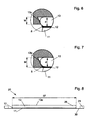
- FIG. 1 shows a semi-automatically usable carrier holder 1, in which the recording of a carrier substrate 13 by the carrier holder 1 is done manually.
- the carrier holder 1 serves to detach the carrier substrate 13 from a product substrate 11 connected to the carrier substrate by a connection layer 12.
- the support bracket 1 consists of a arranged on a peripheral portion 26 handle 2 and an opposite to the handle 2 open ring 3.
- the spacing means 25 for adjusting a distance A is provided between the ends 24, 24 '.
- the spacing means 25 consist in the present embodiment of levers 4, 5, wherein the lever 4 at the end 24 and the lever 5 at the end 24 'are introduced.
- the levers 4, 5 are penetrated by adjusting elements 14, which are manually operated here.
- the attachment of the handle 2 on the ring 3 is effected by fixing elements 10, in particular screws.
- the material of the ring 3 is according to the invention at a given geometry (ring height H, ring width B, outer diameter D a , inner diameter D i ) to be chosen so that the ring 3 can be bent elastically by the spacer means 25, and against its caused by the flexural rigidity Force.
- the ring 3 has a circumferential shoulder 7 which projects from an annular shoulder 6 and forms a step 9.
- the step 9 is Z-shaped with an inner angle directed to the center of the ring 45 ° ⁇ I ⁇ 90 °, in particular ⁇ 80 °, preferably ⁇ 70 ° and thereby forms a, in particular circumferential, wall slope 17, which ends at a sharp inner edge 8.
- the end face 7s is equidistant from the annular shoulder 6 with a distance M.
- the distance M is inventively chosen so that it is at most slightly larger, in particular at most around the Thickness of the connection layer 12 is greater than a thickness d of the carrier substrate 13 (see FIG. 7 ).
- the distance M is as in FIG. 6 is selected to be smaller than the thickness d of the carrier substrate 13.
- the distance M is at least half as large as the thickness d of the carrier substrate 13.
- a diameter D k formed by the inner edge 8 and lying between the inner diameter D i and the outer diameter D a for receiving the carrier substrate 13 can be increased until the carrier substrate 13 is replaced by an opening (diameter D) formed by the inner edge 8 k ) can be used to the annular shoulder 6. Subsequently, the diameter D k is reduced again by the spacing means 25 until a peripheral edge 13u of the carrier substrate 13 bears against the bevel 17 of the peripheral shoulder 7 and is fixed by the latter. Thus, the support substrate 13 is held by the flexible support bracket 1.
- the holder is quasi by clamping and / or positive connection. at Clamping of the carrier substrate 13 on the slope 17 can be provided with force measuring means for controlling the entrapment, in particular on the adjusting means 14.
- the product substrate 11 is attached to the carrier mount only via the tie layer 12. Direct contact between the carrier holder 1 and the product substrate 11 is not provided. By avoiding contact between the support bracket 1 and the product substrate 11, the product substrate 11 is maximally protected and contamination or damage is practically eliminated.
- the product substrate 11 forms with the connection layer 12 and the carrier substrate 13 a stack 19 (carrier substrate - product substrate - composite).
- the present invention is suitable for a composite of carrier substrate and product substrate without intermediate connecting layer, in particular in so-called pre-bonds, in which the wafers adhere to one another, in particular by means of van der Waals forces.
- the pointed inner edge 8 is used in the fixation of the stack 19 to the support bracket 1 in the in FIG. 7 shown embodiment as a release agent or to initiate the release by the tip of the inner edge 8 at the peripheral edge of the bonding layer 12 penetrates into the bonding layer 12.
- the carrier holder 1 encloses the carrier substrate 13 virtually completely, with the exception of the ring opening 3o.
- FIG. 8 shows the stack 19 on a film frame 23, wherein the product substrate 11 is connected to a film 21 connected to the film frame 23.
- the stack 19, the film frame 23 and the film 21 a film frame composite 20th
- the carrier substrate 13 is removable from the product substrate 11.
- the tensile force is applied laterally on the carrier substrate 13, that is on the peripheral portion 26, by the one-sided arrangement of the handle 2. Initiated by the penetration of the inner edge 8 into the connecting layer 12, the carrier substrate 13 is slowly removed from the peripheral section 26 to the opposite side while deforming the carrier substrate 13 and the ring 3 (counter to their force generated by the flexural strength). In this case, a release front of the peripheral portion 26 migrates to the opposite side of the carrier substrate 13 through the connecting layer 12. Along the release front thus act depending on the distance of the release front of the handle 2 and the applied on the handle 2 release force defined torques.
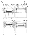
- FIGS. 9a to 9d in a first embodiment and in the FIGS. 10a to 10d shown in a second embodiment, which will be described in more detail below.
- An essential aspect of the invention is to provide a particularly gentle treatment at the beginning of the detachment, that is to say when initiating the detachment, in particular by implementing a mechanical release of the bonding layer on the circumference or at its edge.
- a base 27 and a frame 22 based thereon for the provision of a stable basic construction and fastening of further, below-described components of the device according to the invention are shown.
- the drive means 15 ' may have a freewheel in the translation direction, in particular formed by a floating bearing.
- the substrate holder 18 is according to both embodiments FIG. 9 and FIG. 10 in a release direction L, ie in the drawing plane up and / or down translationally movable.
- the drive means 15 for driving the substrate holder 18 can in particular be moved synchronously, preferably driven by motors controlled by a central control device, in particular stepper motors.
- the carrier support 1 suitable for the film frame assembly 20, in particular the carrier substrate 13, is attached to the upper drive means 15 'and the pivot bearing 16.
- the substrate holder 18 is movable by the drive means 15 in the release direction L.
- the carrier holder 1 can be fixed to the drive means 15 'and the pivot bearing 16 by holding means 28 arranged on the ring circumference 3u.
- the substrate holder 18 can be fixed by holding means 29 to the drive means 15.
- the substrate holder 18 in the in FIG. 9b shown position (ie in the release direction L to the support bracket 1 back) method by the drive means 15 perform a synchronous translational movement of the substrate holder 18 until the carrier substrate 13 abuts with its upper side 13o on the annular shoulder 6.
- the control can take place via the central control device, wherein the detection of the impingement of the carrier substrate 13 on the annular shoulder 6 by, in particular in the substrate holder 18 integrated force measuring means takes place.
- a number n load cells are arranged distributed at an angular distance of 360 ° / n at the periphery of the substrate holder 18.
- the diameter D k on the inner edge 8 of the ring 3 must be correspondingly adapted beforehand so that the carrier substrate 13 with its outer contour (in particular circular with a diameter D t ) can be received in the carrier holder 1 ,
- the inner diameter D i is smaller than the diameter D t of the carrier substrate 13, so that the carrier substrate 13 does not slip.
- the inner diameter D i can be reduced until the support substrate 13 is fixed in the support bracket 1 (see FIGS. 6 and 7 ), that is applied to the wall slope 17.
- the upper, fixable drive means 15 ' is released so that it has a degree of freedom in the release direction L and the drive means 15' attached to the side of the support bracket 1 in the release direction L is freely movable.
- the drive means 15 ' is formed without drive.
- control of the movement by the central control device is also conceivable here, so that the drive means 15 'is not formed passively (as in the preferred embodiment), but actively.
- each one of the support bracket 1 directed away drive force F 1 (tensile force) and, in particular with the driving force F 1 identical, driving force F 2 (tensile force), in particular synchronously, for releasing the carrier substrate 1 fixed to the carrier substrate 1 from the product substrate 11.
- a counterforce G (or a plurality of opposing forces G, if several pivot bearings 16 are provided) abuts on the pivot bearing 16.
- a release front extends from the spherical bearing 16 to the opposite side of the carrier holder 1 with increasing bending of the carrier holder 1 and of the carrier substrate 13.
- the release front act in equilibrium with the driving forces F 1 and F 2 and the (caused by the connection force of the connecting layer 12) counterforce G torques as infinitesimal along the release front distributed loosening moments K 1 to K n .
- connection layer 12 adheres to the product substrate 11 in the illustration, but may also partially or completely adhere to the carrier substrate 13.
- the carrier holder 1 and the carrier substrate 13 bend about a (average, in particular measured at half separation of the carrier substrate 13 from the product substrate 11) bending angle 1 ° ⁇ W ⁇ 45 °, in particular W ⁇ 35 ° here about 6 °.
- a pivot bearing 16 is provided on the carrier holder 1, so that the carrier holder 1 is fixated in the release direction L on the peripheral portions 26 and an opposite peripheral portion 26' (ie, where the pivot bearings 16 are attached to holding means 28 of the carrier holder 1) (According to the invention, a plurality of joint bearings 16 may be provided on the circumference of the carrier holder 1). In sections between the peripheral portions 26, the support bracket 1 is movable in the context of its flexibility against the flexural rigidity. Thus, when the driving forces are applied in the method step according to FIG.
- connection layer 12 a substantially (corrugated) concentrically extending from the periphery of the connecting layer 12 dissolving front to the middle of the connecting layer 12.
- the release moments K l to K n act according to the embodiment FIGS. 10a to 10d as the dissolution front progresses, predominantly on a (corrugated) circular section along the release front.
- the Bending angle W according to FIG. 9c is measured to the hinge bearing opposite side edge, the bending angle W 'is measured because of the circumferentially acting from all sides release force K from the center of the support substrate 13 to the edge, the bending angle W' is correspondingly smaller in this case because of the smaller distance, as far as the material the carrier holder 1 and the carrier substrate 2 and their dimensions are otherwise identical.
Description
Die Erfindung betrifft eine biegsame Trägerhalterung gemäß Patentanspruch 1, eine Vorrichtung zum Lösen eines Trägersubstrats von einem Produktsubstrat in einer Löserichtung L gemäß Patentanspruch 2, ein korrespondierendes Verfahren gemäß Patentanspruch 9 und eine Verwendung einer biegsamen Trägerhalterung zur Halterung eines Trägersubstrats beim Ablösen des Trägersubstrats von einem Produktsubstrat gemäß Patentanspruch 10.The invention relates to a flexible carrier mount according to
In der Halbleiterindustrie werden Strukturwafer beziehungsweise Produktwafer häufig temporär auf Trägerwafer beziehungsweise Trägersubstrate gebondet, um sie handhaben zu können. Nach Prozessierung der Produktsubstrate sollen diese möglichst einfach, schnell und kostengünstig sowie sauber von dem Trägersubstrat entfernt werden. Das am häufigsten eingesetzte Verfahren zum Bonden von Produktwafern auf einem Trägerwafer ist die Aufbringung einer Adhäsionsschicht auf einem der beiden Substrate (oder beiden Substraten) und Kontaktierung unter Druck. Beim Ablösen (Debonding) wird der Trägerwafer nach Reduzierung der Adhäsionskraft des Klebers (Temperatur, UV-Strahlung etc.) vom Produktwafer abgelöst, beispielsweise durch paralleles Verschieben der Wafer gegeneinander. Die Wafer werden dabei durch sogenannte Chucks durch Unterdruck gehalten.In the semiconductor industry, structural wafers or product wafers are often temporarily bonded to carrier wafers or carrier substrates in order to be able to handle them. After processing the product substrates, they should be removed from the carrier substrate as simply, quickly and cost-effectively as possible. The most commonly used method of bonding product wafers to a carrier wafer is to apply an adhesion layer to one of the two substrates (or both substrates) and contact under pressure. During debonding, the carrier wafer is detached from the product wafer after reducing the adhesive force of the adhesive (temperature, UV radiation, etc.), for example by moving the wafers parallel to one another. The wafers are held by so-called chucks by negative pressure.
Dokument
Beim Debonden sind eine Vielzahl kritischer Faktoren zu berücksichtigen und oberste Priorität besteht darin, den brüchigen und auf Grund der Vorbearbeitung sehr teuren Produktwafer möglichst geringem Stress auszusetzen und diesen nicht zu beschädigen. Das Ablösen des Trägersubstrats soll auf der anderen Seite kostengünstig und schnell mit geringst möglichem Energieaufwand erfolgen. Bei einer Vielzahl von bekannten Ablöseprozessen ist es erforderlich, insbesondere zur Auflösung der Adhäsionseigenschaften der Adhäsionsschicht zwischen den Wafern, den "Stack" (Stapel) aus Trägerwafer und Strukturwafer/Produktwafer auf eine für den Kleber spezifische Temperatur aufzuheizen.When debonding a variety of critical factors are taken into account and the top priority is to suspend the fragile and due to the pre-processing very expensive product wafer as low as possible stress and not to damage it. The detachment of the carrier substrate should be done on the other side cost and quickly with the least possible energy. In a variety of known peeling processes, it is necessary, especially for dissolving the adhesion properties of the adhesion layer between the wafers, to heat the "stack" of carrier wafers and structural wafers / product wafers to a temperature specific to the adhesive.
Aufgabe der vorliegenden Erfindung ist es daher, die gattungsgemäßen Vorrichtungen und Verfahren zum Ablösen von Trägersubstraten derart weiterzubilden, dass ein schonendes und gleichzeitig deutlich schnelleres Ablösen ermöglicht wird. Gleichzeitig soll der Energieverbrauch reduziert werden.Object of the present invention is therefore to develop the generic devices and methods for detaching carrier substrates such that a gentle and at the same time much faster detachment is possible. At the same time, the energy consumption should be reduced.
Diese Aufgabe wird mit den Merkmalen der Patentansprüche 1, 9 und 10 gelöst. Vorteilhafte Weiterbildungen der Erfindung sind in den Unteransprüchen angegeben. In den Rahmen der Erfindung fallen auch sämtliche Kombinationen aus zumindest zwei von in der Beschreibung, den Ansprüchen und/oder den Zeichnungen angegebenen Merkmalen. Bei Wertebereichen sollen auch innerhalb der genannten Grenzen liegende Werte als Grenzwerte offenbart und in beliebiger Kombination beanspruchbar sein.This object is achieved with the features of
Grundgedanke der vorliegenden Erfindung ist es, eine Trägerhalterung zur Halterung des Trägersubstrats beim Lösen des Trägersubstrats von dem Produktsubstrat so zu konstruieren, dass die Trägerhalterung eine Biegung des Trägersubstrats zulassend ausgebildet ist. Die Trägerhalterung weist erfindungsgemäß eine ausreichende Biegesteifigkeit auf, um eine Lösekraft zum Ablösen des Trägersubstrats vom Produktsubstrat zu bewirken, insbesondere durch Abheben vom Rand des Trägersubstrats her.The basic idea of the present invention is to construct a carrier holder for holding the carrier substrate when releasing the carrier substrate from the product substrate in such a way that the carrier holder is designed to permit a bending of the carrier substrate. According to the invention, the carrier holder has a sufficient bending stiffness in order to bring about a release force for detaching the carrier substrate from the product substrate, in particular by lifting it off from the edge of the carrier substrate.
Erfindungsgemäß soll dabei nur eine leichte Durchbiegung, insbesondere < 45° Biegewinkel, vorzugsweise < 40°, noch bevorzugter < 30°, besonders bevorzugt < 20°, mit noch größerem Vorzug < 10°, mit allergrößtem Vorzug < 5°, erfolgen. Auf diese Weise wird das auch eine gewisse, insbesondere der Trägerhalterung ähnliche, Biegesteifigkeit aufweisende Trägersubstrat und vor allen Dingen das Produktsubstrat vor Beschädigung geschützt. Durch die Biegung wirkt der größte Teil der Lösekraft an der wandernden Lösefront, die insbesondere vom Rand des Trägersubstrats her in Richtung des Zentrums wandert.According to the invention, only a slight deflection, in particular <45 ° bending angle, preferably <40 °, more preferably <30 °, particularly preferably <20 °, with even greater preference <10 °, with very great preference <5 °, take place. In this way, a certain, in particular the support bracket similar bending stiffness-containing carrier substrate and, above all, the product substrate is protected from damage. Due to the bending, most of the dissolving force acts on the migrating release front, which in particular migrates from the edge of the carrier substrate in the direction of the center.
Kern der Erfindung ist daher eine biegsame Trägerhalterung zur Halterung eines Trägersubstrats beim Lösen des Trägersubstrats von einem Produktsubstrat, wobei Lösemittel zum Ablösen des Produktsubstrats unter Biegung des Trägersubstrats an der Trägerhalterung vorgesehen sind.The core of the invention is therefore a flexible carrier holder for holding a carrier substrate when releasing the carrier substrate from a product substrate, wherein solvents for detaching the product substrate are provided under bending of the carrier substrate on the carrier holder.
Erfindungsgemäß denkbar sind also auch vollflächige, nicht ringförmige Ausführungen der Trägerhalterung, insbesondere aus Polymer mit einer gewissen Elastizität beziehungsweise Biegesteifigkeit. Diese würden zur Fixierung und Aufnahme des Trägersubstrats Vakuumdurchgänge aufweisen. Hierbei kann, insbesondere zusätzlich, zur Erhöhung der Haltekraft, eine elektrostatische Fixierung des Trägersubstrats an der Trägerhalterung vorgesehen sein.
Die Trägerhalterung kann auch zumindest teilweise aus Metall, Keramik oder einem Verbundwerkstoff bestehen. Die verwendeten Materialien müssen nur die erfindungsgemäße Funktionalität erlauben.Also conceivable according to the invention are full-surface, non-annular embodiments of the carrier holder, in particular of polymer with a certain elasticity or flexural rigidity. These would have vacuum passages for fixing and receiving the carrier substrate. In this case, in particular in addition to increase the holding force, an electrostatic fixing of the carrier substrate may be provided on the carrier holder.
The support bracket may also be at least partially made of metal, ceramic or a composite material. The materials used must allow only the functionality of the invention.
Als eigenständige Erfindung ist außerdem eine Vorrichtung zum Lösen eines Trägersubstrats von einem Produktsubstrat in einer Löserichtung L mit folgenden Merkmalen vorgesehen:
- einer in Löserichtung L biegsamen Trägerhalterung zur Halterung des Trägersubstrats,
- einer Substrathalterung zur Halterung des Produktsubstrats und
- Lösemitteln zum Ablösen des Trägersubstrats vom Produktsubstrat unter Biegung des Trägersubstrats.
- a support holder which is flexible in the release direction L for holding the carrier substrate,
- a substrate holder for holding the product substrate and
- Solvents for detaching the carrier substrate from the product substrate while bending the carrier substrate.
Die Löserichtung L ist erfindungsgemäß im Wesentlichen, insbesondere genau, normal zur Oberfläche des Trägersubstrats und/oder Produktsubstrats. Eine Biegeachse der Biegung der Trägerhalterung und/oder des von der Trägerhalterung aufgenommenen Trägersubstrats ist normal zur Löserichtung L. Die Biegeachse liegt insbesondere parallel zur Oberfläche des Produktsubstrats und/oder des Trägersubstrats.According to the invention, the release direction L is essentially, in particular exactly, normal to the surface of the carrier substrate and / or product substrate. A bending axis of the bending of the carrier holder and / or of the carrier substrate received by the carrier holder is normal to the release direction L. The bending axis lies in particular parallel to the surface of the product substrate and / or the carrier substrate.
Die erfindungsgemäße Vorrichtung kann in vorteilhafter Ausführung eine Druckkammer umfassen, die mit Überdruck beaufschlagbar ist, um einen mit Unterdruck an der Trägerhalterung fixiertes Trägersubstrat noch stärker an diesem zu fixieren. Der Druck in der Kammer kann dabei > 1 bar, mit Vorzug > 2 bar, mit noch größerem Vorzug > 5 bar, mit noch größerem Vorzug > 10 bar, insbesondere kleiner 100 bar, sein.In an advantageous embodiment, the device according to the invention can comprise a pressure chamber which can be subjected to overpressure in order to fix a carrier substrate, which is fixed with negative pressure to the carrier holder, even more strongly thereon. The pressure in the chamber can thereby be> 1 bar, with preference> 2 bar, with even greater preference> 5 bar, with even greater preference> 10 bar, in particular less than 100 bar.
Gemäß einer vorteilhaften Ausführungsform der Erfindung ist vorgesehen, dass die Trägerhalterung in Löserichtung L elastisch verformbar ist. Durch die Elastizität der Trägerhalterung wird es erfindungsgemäß ermöglicht, die Lösekraft jeweils an der wandernden Lösefront zu konzentrieren, obwohl eine Zugkraft nur am Umfang des Trägersubstrats angelegt wird.According to an advantageous embodiment of the invention, it is provided that the carrier holder in the release direction L is elastically deformable. Due to the elasticity of the carrier holder, it is possible according to the invention to concentrate the release force in each case on the migrating release front, although a tensile force is applied only on the circumference of the carrier substrate.
In einer weiteren vorteilhaften Ausführungsform der Erfindung ist vorgesehen, dass durch die Lösemittel mindestens eine am Umfang der Substrathalterung wirkende Zugkraft und mindestens eine entgegen der Zugkraft am Umfang der Trägerhalterung wirkende Gegenkraft zur Erzeugung von Lösemomenten entlang einer Lösefront anlegbar sind. Hierdurch kann die Gesamtbelastung, insbesondere beim Beginn des Ablösens, reduziert werden. Auf diese Weise wird eine noch stärkere Schonung des Träger- und des Produktsubstrats bewirkt. Es ist dabei insbesondere vorgesehen, dass die Zugkräfte sich, insbesondere durch gleichmäßige Aufbringung von Zugkräften am Umfang der Substrathalterung, zu einer resultierenden Zugkraft im Zentrum der Substrathalterung summieren, während sich die Gegenkraft oder die Gegenkräfte zu einer resultierenden Gegenkraft an einem Rand der Trägerhalterung sowie entsprechenden Lösemomenten an der wandernden Lösefront summieren. Die Trägerhalterung wird demnach gegenüber der Substrathalterung gekippt.In a further advantageous embodiment of the invention, it is provided that at least one tensile force acting on the circumference of the substrate holder and at least one opposing force acting against the tensile force on the circumference of the carrier holder for the generation of loosening moments along a release front can be applied by the solvent. As a result, the total burden, especially at the beginning of the detachment can be reduced. In this way an even greater protection of the carrier and the product substrate is effected. It is particularly provided that the tensile forces, in particular by uniform application of Tensile forces on the circumference of the substrate holder, add up to a resultant tensile force in the center of the substrate holder, while the counterforce or the counter forces add up to a resulting counterforce on an edge of the carrier support and corresponding release moments on the migrating release front. The carrier holder is thus tilted relative to the substrate holder.
Zur noch stärkeren Schonung des Produktsubstrats, insbesondere bei sehr empfindlichen oder sehr teuren Produktsubstraten, ist es erfindungsgemäß vorgesehen, die Substrathalterung als starre, insbesondere das Produktsubstrat vollflächig aufnehmende, Aufnahme auszubilden.For even greater protection of the product substrate, in particular for very sensitive or very expensive product substrates, it is provided according to the invention to form the substrate holder as a rigid, in particular the product substrate over the entire surface receiving.
Gemäß einer weiteren vorteilhaften Ausführungsform der Erfindung ist vorgesehen, die Trägerhalterung als, insbesondere offener, Ring mit verstellbarem Innendurchmesser Di auszubilden. Durch die Ringform lässt sich die Biegesteifigkeit auch durch die Ringgeometrie, insbesondere die Ringbreite B zum Ringdurchmesser Da und/oder zur Höhe H des Rings optimal auf das Trägersubstrat einstellen. Die Ringform bewirkt weiterhin, dass im Bereich der Ringöffnung eine stärkere Bewegungsfreiheit des Trägersubstrats zugelassen wird, so dass ein Zusammenwirken der Biegesteifigkeit der Trägerhalterung und der Biegesteifigkeit des Trägersubstrats erreicht wird. Dabei ist die Biegesteifigkeit der Trägerhalterung insbesondere mindestens gleich oder höher als die Biegesteifigkeit des Trägersubstrats.According to a further advantageous embodiment of the invention, it is provided to form the carrier holder as, in particular open, ring with adjustable inner diameter D i . Due to the ring shape, the flexural rigidity can also be optimally adjusted to the carrier substrate by the ring geometry, in particular the ring width B to the ring diameter D a and / or the height H of the ring. The ring shape further causes a greater freedom of movement of the carrier substrate is allowed in the region of the ring opening, so that an interaction of the flexural rigidity of the carrier holder and the flexural rigidity of the carrier substrate is achieved. In this case, the bending stiffness of the carrier holder is in particular at least equal to or higher than the bending stiffness of the carrier substrate.
Die Biegesteifigkeit der Trägerhalterung ist mit Vorteil erfindungsgemäß derart gewählt, dass diese in einem Bereich zwischen 1/20 bis 20 mal, insbesondere zwischen 1/10 bis 10 mal, vorzugsweise zwischen 1/5 bis 5 mal, noch bevorzugter zwischen ½ bis 2 mal, der Biegesteifigkeit des Trägersubstrats liegt. Als Trägersubstrat kommt insbesondere ein Wafer aus Silizium mit einer Dicke d zwischen 500µm und 750µm, vorzugsweise von 600µm, in Frage. Dieser kann einen Durchmesser Dt von 200 mm oder 300 mm aufweisen.The bending stiffness of the carrier holder is advantageously selected according to the invention such that it is in a range between 1/20 and 20 times, in particular between 1/10 and 10 times, preferably between 1/5 and 5 times, more preferably between 1/2 and 2 times, the flexural rigidity of the carrier substrate is located. As a carrier substrate is in particular a wafer of silicon having a thickness d between 500 .mu.m and 750 .mu.m, preferably from 600μm, in question. This may have a diameter D t of 200 mm or 300 mm.
Dabei ist es von besonderem Vorteil, insbesondere über den gesamten Ringumfang verlaufende, Haltemittel, insbesondere in Form einer zurückspringenden Umfangsschulter, vorzusehen. Somit kann mit einer einfachen geometrischen Form, die kostengünstig herstellbar ist, sowohl die Lösekraft auf das Trägersubstrat, insbesondere am gesamten Umfang des Trägersubstrats, aufgebracht werden und die besonders kritische Initiierung der Lösefront beim Beginn des Ablösens an eine oder mehrere Stellen am Umfang des Trägersubstarts konzentriert werden.It is of particular advantage, in particular over the entire ring circumference extending, holding means, in particular in the form of a recessed circumferential shoulder to provide. Thus, with a simple geometric shape, which is inexpensive to produce, both the release force on the carrier substrate, in particular the entire circumference of the carrier substrate, are applied and concentrated the particularly critical initiation of the release front at the beginning of the detachment at one or more locations on the circumference of the Trägerubstarts become.
In Weiterbildung ist es erfindungsgemäß vorgesehen, dass die Trägerhalterung das Trägersubstrat im Wesentlichen vollständig, insbesondere mindestens zu 98% des Umfangs, vorzugsweise mindestens zu 99%, noch bevorzugter zu mindestens 99,5%, seitlich umschließend ausgebildet ist. Hierdurch wird das Trägersubstrat quasi vollumfänglich gestützt. Die Trägerhalterung ist insbesondere als, vorzugsweise mindestens zu 98% des Umfangs, noch bevorzugter mindestens zu 99%, noch bevorzugter zu mindestens 99,5%, umfangsgeschlossener Ring ausgebildet. Der Ring kann auch aus Einzelsegmenten zusammengesetzt sein.In a further development, it is provided according to the invention that the carrier mount the carrier substrate substantially completely, in particular at least 98% of the circumference, preferably at least 99%, more preferably at least 99.5%, laterally enclosing. As a result, the carrier substrate is virtually fully supported. The carrier holder is designed in particular as, preferably at least 98% of the circumference, more preferably at least 99%, even more preferably at least 99.5%, circumferentially closed ring. The ring can also be composed of individual segments.
Gemäß einer vorteilhaften Ausführungsform weisen die Lösemittel translatorische Antriebsmittel zur Bewirkung einer Translationsbewegung mindestens eines Umfangsabschnitts der Trägerhalterung in Löserichtung L auf.According to an advantageous embodiment, the solvents have translational drive means for effecting a translational movement of at least one circumferential section of the carrier holder in the release direction L.
Als eigenständige Erfindung ist ein Verfahren zum Lösen eines Trägersubstrats von einem Produktsubstrat in einer Löserichtung L mit folgenden Schritten, insbesondere folgendem Ablauf, vorgesehen:
- Halterung des Produktsubstrats mit einer Substrathalterung und Halterung des Trägersubstrats mit einer in Löserichtung L biegsamen Trägerhalterung und
- Ablösen des Trägersubstrats vom Produktsubstrat unter Biegung des Trägersubstrats.
- Mounting of the product substrate with a substrate holder and mounting of the carrier substrate with a in the release direction L flexible carrier holder and
- Detaching the carrier substrate from the product substrate while bending the carrier substrate.
Weiterhin ist erfindungsgemäß eine Verwendung einer biegsamen Trägerhalterung zur Halterung eines Trägersubstrats beim Ablösen des Trägersubstrats von einem Produktsubstrat vorgesehen.Furthermore, according to the invention, a use of a flexible carrier holder for holding a carrier substrate when detaching the carrier substrate from a product substrate is provided.
In vorteilhafter Ausführungsform der Erfindung ist vorgesehen, dass das Ablösen bei einer Temperatur < 200°C, vorzugsweise < 100°C, noch bevorzugter < 50°C, idealerweise bei Umgebungstemperatur, insbesondere ohne vollflächige Aufheizmittel, erfolgt.In an advantageous embodiment of the invention, it is provided that the detachment takes place at a temperature <200 ° C., preferably <100 ° C., more preferably <50 ° C., ideally at ambient temperature, in particular without full-area heating means.
Erfindungsgemäß ist es denkbar, das Ablösen, insbesondere an der Lösefront, zu beschleunigen, indem lokal auf die Lösefront durch die Lösemittel eingewirkt wird, insbesondere durch Trennungsmittel. Die Trennungsmittel können mechanisches Trennen und/oder lokales Aufheizen, vorzugsweise einen gerichteten Heizluftstrom umfassen. Konkret können ein Trennkeil, eine Trennklinge, ein Trenndraht oder ein auf die Lösefront gerichteter, vorzugsweise warmer, Druckluftstrahl einzeln oder kombiniert vorgesehen sein.
Unter einem Trennkeil versteht man ein Werkzeug mit vorzugsweise v-förmigem Profil. Unter einer Trennklinge versteht man ein Werkzeug mit einer extrem scharfen Kante. Der Trenndraht ist ein sehr dünner, mit Vorzug hochfester Draht, welcher durch eine entsprechende Apparatur im gespannten Zustand in der Ebene der Zwischenschicht auf sie zu verschoben wird. Der Trenndraht ist insbesondere als Heizdraht, also beheizbar ausgebildet.According to the invention, it is conceivable to accelerate the detachment, in particular at the release front, by acting locally on the release front by the solvents, in particular by release agents. The separation means may comprise mechanical separation and / or local heating, preferably a directional heating air flow. Specifically, a separating wedge, a separating blade, a separating wire or a preferably compressed, compressed air jet directed towards the release front can be provided individually or in combination.
A separating wedge is understood to mean a tool with a preferably V-shaped profile. A cutting blade is a tool with an extremely sharp edge. The separation wire is a very thin, preferably high-strength wire, which is moved by a corresponding apparatus in the tensioned state in the plane of the intermediate layer to it. The separating wire is designed in particular as a heating wire, that is to say heatable.
Erfindungsgemäß ist auch eine Ausführungsform denkbar, bei der die Lösefront quasi spiralförmig während des Lösens entlang des Umfangs des Produktsubstrats nach innen zum Zentrum verläuft. Dies wird erreicht, indem die am Umfang wirkenden Lösekräfte am Umfang umlaufend gesteigert werden.According to the invention, an embodiment is conceivable in which the release front is quasi spiral-shaped during the loosening along the circumference of the Product substrate extends inwardly to the center. This is achieved by circumferentially increasing the loosening forces acting on the circumference.
Für die erfindungsgemäße Vorrichtung und das erfindungsgemäße Verfahren sowie die erfindungsgemäße Verwendung gelten die beschriebenen Merkmale analog.For the device according to the invention and the method according to the invention as well as the use according to the invention, the features described apply analogously.
Weitere Vorteile, Merkmale und Einzelheiten der Erfindung ergeben sich aus der Beschreibung bevorzugter Ausführungsbeispiele sowie anhand der Zeichnungen. Diese zeigen in:
Figur 1- eine Aufsicht auf eine erfindungsgemäße Trägerhalterung mit einer Schnittlinie A-A,
Figur 2- eine Querschnittsansicht der Trägerhalterung gemäß Schnittlinie A-A aus
Figur 1 , Figur 3- eine Ansicht der Trägerhalterung gemäß
Figur 1 von unten, Figur 4- eine Detailansicht des Details
E aus Figur 2 , - Figur 5a
- eine Seitenansicht eines Stacks aus Trägersubstrat, Verbindungsschicht und Produktsubstrat,
- Figur 5b
- eine Aufsicht eines Stacks aus Trägersubstrat, Verbindungsschicht und Produktsubstrat,
Figur 6- eine
Detailansicht analog Figur 4 mit einer ersten Ausführungsform der Trägerhalterung, Figur 7- eine
Detailansicht analog Figur 4 mit einer zweiten Ausführungsform der Trägerhalterung, Figur 8- ein auf einem Filmrahmen festgelegter Stack,
- Figuren 9a - 9d
- eine erfindungsgemäße Vorrichtung gemäß einer ersten Ausführungsform mit vier erfindungsgemäßen Verfahrensschritten und
- Figuren 10a - 10d
- eine zweite Ausführungsform der erfindungsgemäßen Vorrichtung mit vier Verfahrensschritten.
- FIG. 1
- a plan view of a support bracket according to the invention with a section line AA,
- FIG. 2
- a cross-sectional view of the carrier bracket according to section line AA
FIG. 1 . - FIG. 3
- a view of the carrier bracket according to
FIG. 1 from underneath, - FIG. 4
- a detailed view of the detail E from
FIG. 2 . - FIG. 5a
- a side view of a stack of carrier substrate, bonding layer and product substrate,
- FIG. 5b
- a top view of a stack of carrier substrate, bonding layer and product substrate,
- FIG. 6
- a detailed view analog
FIG. 4 with a first embodiment of the carrier holder, - FIG. 7
- a detailed view analog
FIG. 4 with a second embodiment of the carrier holder, - FIG. 8
- a stack set on a film frame,
- FIGS. 9a-9d
- a device according to the invention according to a first embodiment with four method steps according to the invention and
- FIGS. 10a-10d
- A second embodiment of the device according to the invention with four steps.
In den Figuren sind gleiche oder gleichwirkende Bauteile mit den gleichen Bezugszeichen gekennzeichnet.In the figures, identical or equivalent components are identified by the same reference numerals.
Die Trägerhalterung 1 besteht aus einem an einem Umfangsabschnitt 26 angeordneten Haltegriff 2 und einem gegenüberliegend zum Haltegriff 2 geöffneten Ring 3. An der Öffnung 3o des Rings 3 sind jeweils an den sich gegenüberliegenden Enden 24, 24' des Rings 3 Abstandsmittel 25 zur Einstellung eines Abstands A zwischen den Enden 24, 24' vorgesehen. Durch die Einstellung des Abstands A sind ein innerer Durchmesser Di und ein äußerer Durchmesser Da des Rings 3 einstellbar. Die Abstandsmittel 25 bestehen im vorliegenden Ausführungsbeispiel aus Hebeln 4, 5, wobei der Hebel 4 an dem Ende 24 und der Hebel 5 an dem Ende 24' eingebracht sind. Die Hebel 4, 5 sind von Stellelementen 14 durchsetzt, die hier manuell bedienbar sind. Eine automatische Umsetzung der vorbeschriebenen manuellen Kinematik ist erfindungsgemäß denkbar.The
Die Befestigung des Haltegriffs 2 am Ring 3 erfolgt durch Fixierelemente 10, insbesondere Schrauben. Das Material des Rings 3 ist erfindungsgemäß bei vorgegebener Geometrie (Ringhöhe H, Ringbreite B, Außendurchmesser Da, Innendurchmesser Di) so zu wählen, dass der Ring 3 sich durch die Abstandsmittel 25 elastisch verbiegen lässt, und zwar entgegen seiner durch die Biegesteifigkeit bewirkten Kraft.The attachment of the
Der Ring 3 weist eine Umfangsschulter 7 auf, die von einem Ringabsatz 6 absteht und eine Stufe 9 bildet. Die Stufe 9 verläuft z-förmig mit einem zur Ringmitte gerichteten Innenwinkel 45° < I < 90°, insbesondere < 80°, vorzugsweise < 70° und bildet dadurch eine, insbesondere umlaufende, Wandschräge 17, die an einer spitzen Innenkante 8 endet. Die Innenkante 8 ist gleichzeitig Bestandteil einer parallel zum Ringabsatz 6 verlaufenden Stirnfläche 7s der Umfangsschulter 7. Die Stirnfläche 7s ist äquidistant zu dem Ringabsatz 6 mit einem Abstand M. Der Abstand M ist erfindungsgemäß so gewählt, dass er maximal geringfügig größer, insbesondere maximal um die Dicke der Verbindungsschicht 12 größer, als eine Dicke d des Trägersubstrats 13 ist (siehe
Durch die Abstandsmittel 25 lässt sich ein durch die Innenkante 8 gebildeter, zwischen dem Innendurchmesser Di und dem Außendurchmesser Da liegender, Durchmesser Dk zur Aufnahme des Trägersubstrats 13 vergrößern, bis das Trägersubstrat 13 durch eine durch die Innenkante 8 gebildete Öffnung (Durchmesser Dk) bis zum Ringabsatz 6 einsetzbar ist. Anschließend wird durch die Abstandsmittel 25 der Durchmesser Dk wieder verringert, bis eine Umfangskante 13u des Trägersubstrats 13 an der Schräge 17 der Umfangsschulter 7 anliegt und durch diese fixiert wird. Somit ist das Trägersubstrat 13 von der biegsamen Trägerhalterung 1 gehalten. Die Halterung erfolgt quasi durch Klemmung und/oder Formschluss. Bei Klemmung des Trägersubstrats 13 an der Schräge 17 können Kraftmessmittel zur Steuerung der Einklemmung vorgesehen sein, insbesondere an den Stellmitteln 14.By means of the spacing means 25, a diameter D k formed by the
Das Produktsubstrat 11 ist nur über die Verbindungsschicht 12 an der Trägerhalterung befestigt. Ein direkter Kontakt zwischen der Trägerhalterung 1 und dem Produktsubstrat 11 ist nicht vorgesehen. Bei Vermeidung eines Kontakts zwischen der Trägerhalterung 1 und dem Produktsubstrat 11 wird das Produktsubstrat 11 maximal geschont und eine Kontamination oder Beschädigung praktisch ausgeschlossen.The
Das Produktsubstrat 11 bildet mit der Verbindungsschicht 12 und dem Trägersubstrat 13 einen Stack 19 (Trägersubstrat - Produktsubstrat - Verbund). Ebenso ist die vorliegende Erfindung geeignet für einen Verbund aus Trägersubstrat und Produktsubstrat ohne dzwischenliegende Verbindungsschicht, insbesondere bei sogennnten Pre-Bonds, bei welchen die Wafer insbesondere mittels Van-der-Waals-Kräften aneinander haften.The
Die spitze Innenkante 8 dient bei der Fixierung des Stacks 19 an der Trägerhalterung 1 in der in
Die Trägerhalterung 1 umschließt das Trägersubstrat 13 praktisch vollständig, mit Ausnahme der Ringöffnung 3o.The
Mittels des Haltegriffs 2 und durch Fixierung des Produktsubstrats 11 oder des Filmrahmens 23 ist das Trägersubstrat 13 von dem Produktsubstrat 11 abziehbar. Die Zugkraft wird dabei durch die einseitige Anordnung des Haltegriffs 2 seitlich an dem Trägersubstrat 13, also an dem Umfangsabschnitt 26, aufgebracht. Initiiert durch das Eindringen der Innenkante 8 in die Verbindungsschicht 12 wird das Trägersubstrat 13 unter Verformung des Trägersubstrats 13 und des Rings 3 (entgegen deren durch die Biegesteifigkeit erzeugten Kraft) ausgehend von dem Umfangsabschnitt 26 zur gegenüberliegenden Seite langsam abgelöst. Dabei wandert eine Lösefront von dem Umfangsabschnitt 26 bis zur gegenüberliegenden Seite des Trägersubstrats 13 durch die Verbindungsschicht 12. Entlang der Lösefront wirken demnach je nach Abstand der Lösefront vom Haltegriff 2 und der am Haltegriff 2 angelegten Lösekraft definierte Drehmomente.By means of the
In automatisierter Form ist dies in den
Den beiden Ausführungsformen gemein ist die Verwendung der oben beschriebenen Trägerhalterung 1 zur Halterung des Trägersubstrats 13 in einer zur Automatisierung geeigneten Form.Common to the two embodiments is the use of the
Ein wesentlicher Erfindungsaspekt besteht darin, beim Beginn des Ablösens, also bei der Initiierung des Ablösens, eine besonders schonende Behandlung vorzusehen, insbesondere durch Implementierung einer mechanischen Anlösung der Verbindungsschicht am Umfang beziehungsweise an deren Rand.An essential aspect of the invention is to provide a particularly gentle treatment at the beginning of the detachment, that is to say when initiating the detachment, in particular by implementing a mechanical release of the bonding layer on the circumference or at its edge.
In den
Die Substrathalterung 18 ist bei beiden Ausführungsformen gemäß
In der Ausführungsform gemäß
In dem in
Erfindungsgemäß ist des dabei alternativ denkbar, dass am Umfang der Trägerhalterung 1 mehrere, insbesondere zwei, Antriebsmittel 15' an einer Seite und mehrere, insbesondere zwei, Gelenklager 16 an der gegenüberliegenden Seite, vorgesehen sind.According to the invention, it is alternatively conceivable that a plurality of, in particular two, drive means 15 'are provided on one side and a plurality, in particular two,
Die Trägerhalterung 1 ist jeweils durch am Ringumfang 3u angeordnete Haltemittel 28 an dem Antriebsmittel 15' und dem Gelenklager 16 fixierbar. Die Substrathalterung 18 ist durch Haltemittel 29 an den Antriebsmitteln 15 fixierbar.The
Anschließend wird die Substrathalterung 18 in die in
Damit das Trägersubstrat 13 in der Trägerhalterung 1 aufnehmbar ist, muss vorher der Durchmesser Dk an der Innenkante 8 des Rings 3 entsprechend angepasst werden, damit das Trägersubstrat 13 mit seiner Außenkontur (insbesondere kreisförmig mit einem Durchmesser Dt) in die Trägerhalterung 1 aufnehmbar ist. Der Innendurchmesser Di ist bei der Aufnahme des Trägersubstrats 13 kleiner als der Durchmesser Dt des Trägersubstrats 13, damit das Trägersubstrat 13 nicht durchrutscht. Sobald die in
Sobald die in
Anschließend wird an den beiden gegenüberliegend an der Substrathalterung 18 vorgesehenen Antriebsmitteln 15 auf die Substrathalterung 18 jeweils eine von der Trägerhalterung 1 weg gerichtete Antriebskraft F1 (Zugkraft) und eine, insbesondere mit der Antriebskraft F1 identische, Antriebskraft F2 (Zugkraft), insbesondere synchron, zum Ablösen des an der Trägerhalterung 1 fixierten Trägersubstrats 13 von dem Produktsubstrat 11 angelegt.Subsequently, at the two opposite to the
Entgegen der Antriebskräfte F1 und F2 und insbesondere parallel zu diesen wirkend liegt an dem Gelenklager 16 eine Gegenkraft G (oder mehrere Gegenkräfte G, falls mehrere Gelenklager 16 vorgesehen sind) an.Contrary to the driving forces F 1 and F 2 and in particular acting parallel to these, a counterforce G (or a plurality of opposing forces G, if
Hierdurch wird der von der Innenkante 8 initiierte Ablösevorgang fortgesetzt, wobei an der sich vom Gelenklager 16 bis zur gegenüberliegenden Seite der Trägerhalterung 1 eine Lösefront unter zunehmender Biegung der Trägerhalterung 1 und des Trägersubstrats 13 verläuft. Entlang der Lösefront wirken im Gleichgewicht mit den Antriebskräften F1 und F2 sowie der (durch die Verbindungskraft der Verbindungsschicht 12 bewirkte) Gegenkraft G Drehmomente als infinitesimal entlang der Lösefront verteilte Lösemomente K1 bis Kn.As a result, the detachment process initiated by the
In der in
In der in
Während des Ablösens verbiegt sich die Trägerhalterung 1 und das Trägersubstrat 13 um einen (mittleren, insbesondere gemessen bei halber Ablösung des Trägersubstrats 13 vom Produktsubstrat 11) Biegewinkel 1° < W < 45°, insbesondere W < 35° hier etwa 6°.During the detachment, the
In der zweiten Ausführungsform gemäß
Die Lösemomente Kl bis Kn wirken bei der Ausführungsform gemäß
- 11
- Trägerhalterungcarrier holder
- 22
- Haltegriffhandle
- 33
- Ringring
- 3o3o
- Öffnungopening
- 3u3u
- Ringumfangring circumference
- 44
- Hebellever
- 55
- Hebellever
- 66
- Ringabsatzannular shoulder
- 77
- Umfangsschulterperipheral shoulder
- 7s7s
- Stirnflächeface
- 88th
- Innenkanteinner edge
- 99
- Stufestep
- 1010
- Fixiermittelfixer
- 1111
- Produktsubstratproduct substrate
- 1212
- Verbindungsschichtlink layer
- 1313
- Trägersubstratcarrier substrate
- 13o13o
- Oberseitetop
- 13u13u
- Umfangskanteperipheral edge of
- 1414
- Stellelementeactuators
- 15, 15'15, 15 '
- Antriebsmitteldrive means
- 1616
- GelenklagerSpherical plain bearings
- 1717
- Schrägeslope
- 1818
- Substrathalterungsubstrate holder
- 1919
- Stackstack
- 2020
- FilmrahmenverbundFilm frame composite
- 2121
- Foliefoil
- 2222
- Gestellframe
- 22d22d
- Deckelcover
- 2323
- Filmrahmenfilm frame
- 24, 24'24, 24 '
- Endenend up
- 2525
- Abstandsmittelspacer
- 2626
- Umfangsabschnittperipheral portion
- 2727
- BasisBase
- 27b27b
- Bodenground
- 2828
- Haltemittelholding means
- 2929
- Haltemittelholding means
- AA
- Abstanddistance
- BB
- Ringbreitering width
- Di D i
- InnendurchmesserInner diameter
- Da D a
- Außendurchmesserouter diameter
- Dk D k
- Durchmesserdiameter
- HH
- Ringhöhering height
- MM
- Abstanddistance
- LL
- Löserichtungrelease direction
- II
- Innenwinkelinterior angle
- dd
- Dickethickness
- F1, F2, Fn F 1 , F 2 , F n
- Antriebskräfte (Zugkraft)Driving forces (tensile force)
- GG
- Gegenkraftcounterforce
- K1, K2, Kn K 1 , K 2 , K n
- Lösemomenteloosening moments
- W, W'W, W '
- Biegungswinkelbending angle
Claims (10)
- Flexible carrier mount (1) for mounting of a carrier substrate (13) when the carrier substrate (13) is detached from a product substrate (11), detachment means (1, 28) being provided for debonding of the product substrate (11) with bending of the carrier substrate (13), characterized in that the carrier mount (1) is designed to allow bending of the carrier substrate (13) and made as an open ring (3) with an adjustable diameter (Dk).
- Device for detaching a carrier substrate (13) from a product substrate (11) in one detachment direction (L) with the following features:- a carrier mount (1) which is flexible in the detachment direction (L) for mounting of the carrier substrate (13),- a substrate mount (18) for mounting of the product substrate (11) and- detachment means (1, 15, 15', 16, 28) for debonding of the carrier substrate (13) from the product substrate (1) with bending of the carrier substrate (11), wherein the carrier mount (1) is designed to allow bending of the carrier substrate (13) and made as an open ring (3) with an adjustable diameter (Dk)..
- Device as claimed in Claim 2, the carrier mount (1) being elastically deformable in the detachment direction (L).
- Device as claimed in Claim 2 or 3, wherein at least one tensile force (F1, F2, Fn) acting especially on the periphery of the substrate mount (18) and at least one opposing force (G) acting against the tensile force (F1, F2, Fn), especially on the periphery of the carrier mount can be applied by the detachment means (1, 15, 15', 16, 28) to produce detachment moments (L1, L2, Ln) along one detachment front.
- Device as claimed in one of Claims 2 to 4, wherein the substrate mount (18) is made as a rigid substrate mount (18) which accommodates the product substrate (11) over the entire surface.
- Carrier mount as claimed in Claim 1, wherein the carrier mount (1) is made as an open ring (3).
- Carrier mount as claimed in one of Claims 1 or 6, which has holding means (9) which run especially over the entire ring periphery (3u), especially with a rebounding peripheral shoulder (7).
- Carrier mount as claimed in one of Claims 1, or 7, which is made to laterally enclose the carrier substrate (13) essentially completely.
- Method for detaching a carrier substrate from a product substrate in one detachment direction (L) with the following steps, especially the following sequence:- mounting of the product substrate with a substrate mount and mounting of the carrier substrate with a carrier mount which is flexible in the detachment direction (L) and which is designed to allow bending of the carrier substrate 813) and made as an open ring (3) with an adjustable diameter (Dk), and- debonding of the carrier substrate from the product substrate with bending of the carrier substrate.
- Use of a flexible carrier mount for mounting of a carrier substrate when the carrier substrate is debonded from a product substrate, characterized in that the carrier mount (1) is designed to allow bending of the carrier substrate (13) and made as an open ring (3) with an adjustable diameter (Dk).
Applications Claiming Priority (1)
| Application Number | Priority Date | Filing Date | Title |
|---|---|---|---|
| PCT/EP2011/055630 WO2012139627A1 (en) | 2011-04-11 | 2011-04-11 | Bendable carrier mounting, device and method for releasing a carrier substrate |
Publications (2)
| Publication Number | Publication Date |
|---|---|
| EP2697823A1 EP2697823A1 (en) | 2014-02-19 |
| EP2697823B1 true EP2697823B1 (en) | 2014-06-25 |
Family
ID=43982253
Family Applications (1)
| Application Number | Title | Priority Date | Filing Date |
|---|---|---|---|
| EP11713301.7A Active EP2697823B1 (en) | 2011-04-11 | 2011-04-11 | Bendable carrier mounting, device and method for releasing a carrier substrate |
Country Status (8)
| Country | Link |
|---|---|
| US (2) | US9296193B2 (en) |
| EP (1) | EP2697823B1 (en) |
| JP (1) | JP6234363B2 (en) |
| KR (3) | KR20150108428A (en) |
| CN (1) | CN103460369B (en) |
| SG (1) | SG193904A1 (en) |
| TW (3) | TWI610388B (en) |
| WO (1) | WO2012139627A1 (en) |
Cited By (1)
| Publication number | Priority date | Publication date | Assignee | Title |
|---|---|---|---|---|
| EP3382744A1 (en) | 2016-02-16 | 2018-10-03 | EV Group E. Thallner GmbH | Device for bonding substrates |
Families Citing this family (24)
| Publication number | Priority date | Publication date | Assignee | Title |
|---|---|---|---|---|
| KR20150108428A (en) | 2011-04-11 | 2015-09-25 | 에베 그룹 에. 탈너 게엠베하 | Bendable carrier mounting, device and method for releasing a carrier substrate |
| JP2013033925A (en) * | 2011-07-01 | 2013-02-14 | Tokyo Electron Ltd | Cleaning method, program, computer storage medium, cleaning device, and peeling system |
| EP2795669B1 (en) | 2011-12-22 | 2020-06-17 | EV Group E. Thallner GmbH | Flexible substrate holder, device and method for detaching a first substrate |
| KR102007042B1 (en) * | 2012-09-19 | 2019-08-02 | 도쿄엘렉트론가부시키가이샤 | Delamination device |
| JP6014477B2 (en) * | 2012-12-04 | 2016-10-25 | 東京エレクトロン株式会社 | Peeling device, peeling system and peeling method |
| JP5993731B2 (en) * | 2012-12-04 | 2016-09-14 | 東京エレクトロン株式会社 | Peeling device, peeling system and peeling method |
| US10103048B2 (en) * | 2013-08-28 | 2018-10-16 | Brewer Science, Inc. | Dual-layer bonding material process for temporary bonding of microelectronic substrates to carrier substrates |
| CN105934345B (en) | 2014-01-28 | 2017-06-13 | 惠普发展公司,有限责任合伙企业 | Flexible carrier |
| KR102211334B1 (en) * | 2014-01-28 | 2021-02-03 | 에베 그룹 에. 탈너 게엠베하 | Device and method for removing a first substrate |
| US10276409B2 (en) | 2014-06-27 | 2019-04-30 | Erich Thallner | Sample holder, device and method for detaching of a first substrate |
| US9991150B2 (en) | 2014-12-12 | 2018-06-05 | Micro Materials Inc. | Procedure of processing a workpiece and an apparatus designed for the procedure |
| CN104485294A (en) | 2014-12-12 | 2015-04-01 | 浙江中纳晶微电子科技有限公司 | Temporary bonding and separation method for wafers |
| CN104979262B (en) * | 2015-05-14 | 2020-09-22 | 浙江中纳晶微电子科技有限公司 | Wafer separation method |
| CN106710442B (en) * | 2015-10-21 | 2021-01-22 | 京东方科技集团股份有限公司 | Backlight source separation equipment |
| KR101898121B1 (en) * | 2015-10-22 | 2018-09-12 | 저지앙 마이크로테크 머테리얼 컴퍼니 리미티드 | A procedure of processing a workpiece and an apparatus designed for the precedure |
| CN106739424B (en) * | 2015-11-20 | 2020-02-14 | 财团法人工业技术研究院 | Taking-down and bonding device, taking-down method and bonding method using same |
| JP2018043377A (en) * | 2016-09-13 | 2018-03-22 | 株式会社Screenホールディングス | Peeling device and peeling method |
| US10456008B2 (en) * | 2016-11-29 | 2019-10-29 | Whirlpool Corporation | Learning dispensing system for water inlet hose |
| US10272661B2 (en) * | 2017-04-17 | 2019-04-30 | Taiwan Semiconductor Manufacturing Company, Ltd. | Pad removal device and method |
| TWI648213B (en) * | 2017-11-30 | 2019-01-21 | 景碩科技股份有限公司 | Tear foil mechanism |
| CN108195501B (en) * | 2018-02-12 | 2019-12-20 | 哈尔滨市高新技术检测研究院 | Detection method for ski binding separation moment |
| US11022791B2 (en) | 2018-05-18 | 2021-06-01 | Facebook Technologies, Llc | Assemblies of anisotropic optical elements and methods of making |
| JP7471862B2 (en) | 2020-02-27 | 2024-04-22 | キオクシア株式会社 | Bonding device and bonding method |
| JP7339905B2 (en) | 2020-03-13 | 2023-09-06 | キオクシア株式会社 | Bonding device and bonding method |
Family Cites Families (42)
| Publication number | Priority date | Publication date | Assignee | Title |
|---|---|---|---|---|
| JPH06268051A (en) | 1993-03-10 | 1994-09-22 | Mitsubishi Electric Corp | Wafer stripper |
| US5932048A (en) | 1995-04-06 | 1999-08-03 | Komatsu Electronic Metals Co., Ltd. | Method of fabricating direct-bonded semiconductor wafers |
| JPH1159895A (en) | 1997-08-27 | 1999-03-02 | Matsushita Electric Ind Co Ltd | Board taking-off device, and board taking-off method using this device |
| US5768980A (en) * | 1997-08-29 | 1998-06-23 | Degen; Monika | Baking form assembly |
| FR2783970B1 (en) * | 1998-09-25 | 2000-11-03 | Commissariat Energie Atomique | DEVICE AUTHORIZING THE PROCESSING OF A SUBSTRATE IN A MACHINE PROVIDED FOR PROCESSING LARGER SUBSTRATES AND SYSTEM FOR MOUNTING A SUBSTRATE IN THIS DEVICE |
| US6423613B1 (en) | 1998-11-10 | 2002-07-23 | Micron Technology, Inc. | Low temperature silicon wafer bond process with bulk material bond strength |
| US6431623B1 (en) | 1999-06-11 | 2002-08-13 | Honeywell International Inc. | Vacuum device for peeling off thin sheets |
| US6221740B1 (en) * | 1999-08-10 | 2001-04-24 | Silicon Genesis Corporation | Substrate cleaving tool and method |
| WO2003098695A1 (en) | 2002-05-20 | 2003-11-27 | Sumitomo Mitsubishi Silicon Corporation | Laminated substrate, method of manufacturing the substrate, and wafer outer periphery pressing jigs used for the method |
| US6760985B2 (en) * | 2002-09-03 | 2004-07-13 | David A. Wilson | Craft hoop clamping method and apparatus |
| US7187162B2 (en) | 2002-12-16 | 2007-03-06 | S.O.I.Tec Silicon On Insulator Technologies S.A. | Tools and methods for disuniting semiconductor wafers |
| US20050150597A1 (en) * | 2004-01-09 | 2005-07-14 | Silicon Genesis Corporation | Apparatus and method for controlled cleaving |
| JP2006059861A (en) | 2004-08-17 | 2006-03-02 | Lintec Corp | Transferring and bonding device of brittle member |
| US7381628B2 (en) | 2004-08-20 | 2008-06-03 | Integrated Sensing Systems, Inc. | Process of making a microtube and microfluidic devices formed therewith |
| US7622048B2 (en) * | 2004-10-21 | 2009-11-24 | Fujifilm Dimatix, Inc. | Sacrificial substrate for etching |
| JP4668659B2 (en) | 2005-03-30 | 2011-04-13 | 大日本印刷株式会社 | Joining member and method for producing joining member |
| US20070013014A1 (en) | 2005-05-03 | 2007-01-18 | Shuwen Guo | High temperature resistant solid state pressure sensor |
| US20080032501A1 (en) | 2006-07-21 | 2008-02-07 | Honeywell International Inc. | Silicon on metal for mems devices |
| FR2906933B1 (en) | 2006-10-06 | 2009-02-13 | Commissariat Energie Atomique | DEVICE FOR SEPARATING A STACKED STRUCTURE AND ASSOCIATED METHOD |
| JP4729003B2 (en) * | 2007-06-08 | 2011-07-20 | リンテック株式会社 | Processing method for brittle members |
| KR100891384B1 (en) | 2007-06-14 | 2009-04-02 | 삼성모바일디스플레이주식회사 | Flexible substrate bonding apparatus and debonding apparatus |
| US20090017248A1 (en) * | 2007-07-13 | 2009-01-15 | 3M Innovative Properties Company | Layered body and method for manufacturing thin substrate using the layered body |
| US7682933B1 (en) | 2007-09-26 | 2010-03-23 | The United States Of America As Represented By The Secretary Of The Air Force | Wafer alignment and bonding |
| FR2926671B1 (en) | 2008-01-17 | 2010-04-02 | Soitec Silicon On Insulator | METHOD FOR TREATING DEFECTS WHEN BONDING PLATES |
| KR101096142B1 (en) * | 2008-01-24 | 2011-12-19 | 브레우어 사이언스 인코포레이션 | Method for reversibly mounting a device wafer to a carrier substrate |
| US8459779B2 (en) | 2008-04-11 | 2013-06-11 | Lexmark International, Inc. | Heater chips with silicon die bonded on silicon substrate, including offset wire bonding |
| DE102008018536B4 (en) * | 2008-04-12 | 2020-08-13 | Erich Thallner | Device and method for applying and / or detaching a wafer to / from a carrier |
| US7749884B2 (en) | 2008-05-06 | 2010-07-06 | Astrowatt, Inc. | Method of forming an electronic device using a separation-enhancing species |
| JP2010010207A (en) * | 2008-06-24 | 2010-01-14 | Tokyo Ohka Kogyo Co Ltd | Separating apparatus and separating method |
| JP2010135682A (en) | 2008-12-08 | 2010-06-17 | Sumco Corp | Method and apparatus for manufacturing pasted silicon wafer |
| SG178765A1 (en) | 2009-01-21 | 2012-03-29 | Semiconductor Energy Lab | Method for manufacturing soi substrate and semiconductor device |
| TWI410329B (en) * | 2009-03-09 | 2013-10-01 | Ind Tech Res Inst | Apparatus for releasing a flexible device and method thereof |
| KR20120027237A (en) | 2009-04-16 | 2012-03-21 | 수스 마이크로텍 리소그라피 게엠바하 | Improved apparatus for temporary wafer bonding and debonding |
| US8950459B2 (en) * | 2009-04-16 | 2015-02-10 | Suss Microtec Lithography Gmbh | Debonding temporarily bonded semiconductor wafers |
| US8366873B2 (en) * | 2010-04-15 | 2013-02-05 | Suss Microtec Lithography, Gmbh | Debonding equipment and methods for debonding temporary bonded wafers |
| US20100279435A1 (en) | 2009-04-30 | 2010-11-04 | Applied Materials, Inc. | Temperature control of chemical mechanical polishing |
| US8772627B2 (en) * | 2009-08-07 | 2014-07-08 | Semiconductor Energy Laboratory Co., Ltd. | Photoelectric conversion device and manufacturing method thereof |
| CN102202994B (en) * | 2009-08-31 | 2014-03-12 | 旭硝子株式会社 | Peeling device |
| EP2667407B1 (en) | 2009-09-01 | 2019-01-23 | EV Group GmbH | Method for releasing a product substrate (e.g., a semiconductor wafer) from a support substrate using a solvent and acoustic waves by deformation of a flexible film mounted on a frame |
| US8852391B2 (en) | 2010-06-21 | 2014-10-07 | Brewer Science Inc. | Method and apparatus for removing a reversibly mounted device wafer from a carrier substrate |
| KR20150108428A (en) | 2011-04-11 | 2015-09-25 | 에베 그룹 에. 탈너 게엠베하 | Bendable carrier mounting, device and method for releasing a carrier substrate |
| EP2795669B1 (en) | 2011-12-22 | 2020-06-17 | EV Group E. Thallner GmbH | Flexible substrate holder, device and method for detaching a first substrate |
-
2011
- 2011-04-11 KR KR1020157024328A patent/KR20150108428A/en not_active Application Discontinuation
- 2011-04-11 US US14/008,696 patent/US9296193B2/en active Active
- 2011-04-11 WO PCT/EP2011/055630 patent/WO2012139627A1/en active Application Filing
- 2011-04-11 JP JP2014504171A patent/JP6234363B2/en active Active
- 2011-04-11 KR KR1020177017651A patent/KR20170078858A/en active Search and Examination
- 2011-04-11 SG SG2013068564A patent/SG193904A1/en unknown
- 2011-04-11 EP EP11713301.7A patent/EP2697823B1/en active Active
- 2011-04-11 CN CN201180070028.7A patent/CN103460369B/en active Active
- 2011-04-11 KR KR1020137026190A patent/KR101570917B1/en active IP Right Grant
-
2012
- 2012-01-19 TW TW104131062A patent/TWI610388B/en active
- 2012-01-19 TW TW106134784A patent/TWI641068B/en active
- 2012-01-19 TW TW101102305A patent/TWI511224B/en active
-
2015
- 2015-09-30 US US14/870,139 patent/US10272660B2/en active Active
Cited By (8)
| Publication number | Priority date | Publication date | Assignee | Title |
|---|---|---|---|---|
| EP3382744A1 (en) | 2016-02-16 | 2018-10-03 | EV Group E. Thallner GmbH | Device for bonding substrates |
| US10109487B2 (en) | 2016-02-16 | 2018-10-23 | Ev Group E. Thallner Gmbh | Method for bonding substrates |
| US10504730B2 (en) | 2016-02-16 | 2019-12-10 | Ev Group E. Thallner Gmbh | Device and method for bonding of substates |
| US10636662B2 (en) | 2016-02-16 | 2020-04-28 | Ev Group E. Thallner Gmbh | Device and method for bonding of substrates |
| US10748770B2 (en) | 2016-02-16 | 2020-08-18 | Ev Group E. Thallner Gmbh | Device and method for bonding of substrates |
| US10861699B2 (en) | 2016-02-16 | 2020-12-08 | Ev Group E. Thallner Gmbh | Device and method for bonding of substrates |
| US11251045B2 (en) | 2016-02-16 | 2022-02-15 | Ev Group E. Thallner Gmbh | Device and method for bonding of substrates |
| US11527410B2 (en) | 2016-02-16 | 2022-12-13 | Ev Group E. Thallner Gmbh | Device and method for bonding of substrates |
Also Published As
| Publication number | Publication date |
|---|---|
| TW201601234A (en) | 2016-01-01 |
| KR20150108428A (en) | 2015-09-25 |
| US20160020124A1 (en) | 2016-01-21 |
| CN103460369A (en) | 2013-12-18 |
| JP6234363B2 (en) | 2017-11-22 |
| US10272660B2 (en) | 2019-04-30 |
| US9296193B2 (en) | 2016-03-29 |
| US20140020847A1 (en) | 2014-01-23 |
| CN103460369B (en) | 2016-12-28 |
| KR20170078858A (en) | 2017-07-07 |
| TW201802995A (en) | 2018-01-16 |
| TWI610388B (en) | 2018-01-01 |
| SG193904A1 (en) | 2013-11-29 |
| WO2012139627A1 (en) | 2012-10-18 |
| TWI641068B (en) | 2018-11-11 |
| EP2697823A1 (en) | 2014-02-19 |
| TW201241954A (en) | 2012-10-16 |
| KR20140001998A (en) | 2014-01-07 |
| JP2014513426A (en) | 2014-05-29 |
| KR101570917B1 (en) | 2015-11-20 |
| TWI511224B (en) | 2015-12-01 |
Similar Documents
| Publication | Publication Date | Title |
|---|---|---|
| EP2697823B1 (en) | Bendable carrier mounting, device and method for releasing a carrier substrate | |
| EP2795669B1 (en) | Flexible substrate holder, device and method for detaching a first substrate | |
| DE102008018536B4 (en) | Device and method for applying and / or detaching a wafer to / from a carrier | |
| EP2230683B1 (en) | Device and method for releasing a wafer from a holder | |
| AT503053B1 (en) | COMBINATION OF A CARRIER AND A WAFER | |
| DE602005001950T2 (en) | Method and apparatus for holding a thin and flexible plate with multiple suction cups | |
| AT502233B1 (en) | Carrier detachment device aligns inner, near-edge surface of frame with semiconductor disk and bonds them to foil, before detaching disk from carrier | |
| EP2422357B1 (en) | Device and method for separating a substrate from a carrier substrate | |
| DE112013000980B4 (en) | Method for temporarily connecting a product substrate to a carrier substrate and a corresponding composite | |
| DE112014005278B4 (en) | Device and method for releasing a carrier wafer | |
| AT503848A2 (en) | HANDLING DEVICE AND HANDLING METHOD FOR WAFER | |
| DE112010000454B4 (en) | TRANSPORT ROLL WITH END CAPS | |
| DE102017120243A1 (en) | Method and device for applying a component to a component by means of a manipulator | |
| EP2620637B1 (en) | Lock device for a powertrain of a wind energy assembly and method for locking the powertrain | |
| EP1766419B1 (en) | Device for automatically isolating and treating cell clones | |
| DE102017100456B4 (en) | Manipulator for applying, in particular for pressing, a component to a component | |
| DE102018102766B4 (en) | Support device for a flat substrate and arrangement of a handling device and such a carrier device | |
| EP2596525B1 (en) | Handling device for handling a wafer | |
| AT516595B1 (en) | Device and method for applying and / or detaching a wafer to / from a carrier | |
| WO2013097894A1 (en) | Method and device for bonding of substrates | |
| DE102020210751A1 (en) | METHOD OF REMOVING A CARRIER PLATE | |
| EP2828885B9 (en) | Pressure transfer plate for pressure transfer of a bonding pressure | |
| DE102005047509B4 (en) | Device for separating a planar object from a body to which the object is connected by means of adhesion | |
| EP3348383A1 (en) | Method and device for applying an element to a component part by use of a manipulator | |
| WO2016041644A1 (en) | Device and method for detaching a product substrate from a carrier substrate |
Legal Events
| Date | Code | Title | Description |
|---|---|---|---|
| PUAI | Public reference made under article 153(3) epc to a published international application that has entered the european phase |
Free format text: ORIGINAL CODE: 0009012 |
|
| 17P | Request for examination filed |
Effective date: 20130814 |
|
| AK | Designated contracting states |
Kind code of ref document: A1 Designated state(s): AL AT BE BG CH CY CZ DE DK EE ES FI FR GB GR HR HU IE IS IT LI LT LU LV MC MK MT NL NO PL PT RO RS SE SI SK SM TR |
|
| GRAP | Despatch of communication of intention to grant a patent |
Free format text: ORIGINAL CODE: EPIDOSNIGR1 |
|
| RIC1 | Information provided on ipc code assigned before grant |
Ipc: H01L 21/67 20060101AFI20140224BHEP Ipc: B32B 43/00 20060101ALI20140224BHEP Ipc: H01L 21/687 20060101ALI20140224BHEP Ipc: H01L 21/683 20060101ALI20140224BHEP |
|
| DAX | Request for extension of the european patent (deleted) | ||
| INTG | Intention to grant announced |
Effective date: 20140318 |
|
| GRAS | Grant fee paid |
Free format text: ORIGINAL CODE: EPIDOSNIGR3 |
|
| GRAA | (expected) grant |
Free format text: ORIGINAL CODE: 0009210 |
|
| AK | Designated contracting states |
Kind code of ref document: B1 Designated state(s): AL AT BE BG CH CY CZ DE DK EE ES FI FR GB GR HR HU IE IS IT LI LT LU LV MC MK MT NL NO PL PT RO RS SE SI SK SM TR |
|
| REG | Reference to a national code |
Ref country code: GB Ref legal event code: FG4D Free format text: NOT ENGLISH |
|
| REG | Reference to a national code |
Ref country code: CH Ref legal event code: EP |
|
| REG | Reference to a national code |
Ref country code: AT Ref legal event code: REF Ref document number: 675152 Country of ref document: AT Kind code of ref document: T Effective date: 20140715 |
|
| REG | Reference to a national code |
Ref country code: IE Ref legal event code: FG4D Free format text: LANGUAGE OF EP DOCUMENT: GERMAN |
|
| REG | Reference to a national code |
Ref country code: DE Ref legal event code: R096 Ref document number: 502011003553 Country of ref document: DE Effective date: 20140807 |
|
| PG25 | Lapsed in a contracting state [announced via postgrant information from national office to epo] |
Ref country code: NO Free format text: LAPSE BECAUSE OF FAILURE TO SUBMIT A TRANSLATION OF THE DESCRIPTION OR TO PAY THE FEE WITHIN THE PRESCRIBED TIME-LIMIT Effective date: 20140925 Ref country code: CY Free format text: LAPSE BECAUSE OF FAILURE TO SUBMIT A TRANSLATION OF THE DESCRIPTION OR TO PAY THE FEE WITHIN THE PRESCRIBED TIME-LIMIT Effective date: 20140625 Ref country code: GR Free format text: LAPSE BECAUSE OF FAILURE TO SUBMIT A TRANSLATION OF THE DESCRIPTION OR TO PAY THE FEE WITHIN THE PRESCRIBED TIME-LIMIT Effective date: 20140926 Ref country code: FI Free format text: LAPSE BECAUSE OF FAILURE TO SUBMIT A TRANSLATION OF THE DESCRIPTION OR TO PAY THE FEE WITHIN THE PRESCRIBED TIME-LIMIT Effective date: 20140625 Ref country code: LT Free format text: LAPSE BECAUSE OF FAILURE TO SUBMIT A TRANSLATION OF THE DESCRIPTION OR TO PAY THE FEE WITHIN THE PRESCRIBED TIME-LIMIT Effective date: 20140625 |
|
| REG | Reference to a national code |
Ref country code: NL Ref legal event code: VDEP Effective date: 20140625 |
|
| REG | Reference to a national code |
Ref country code: LT Ref legal event code: MG4D |
|
| PG25 | Lapsed in a contracting state [announced via postgrant information from national office to epo] |
Ref country code: SE Free format text: LAPSE BECAUSE OF FAILURE TO SUBMIT A TRANSLATION OF THE DESCRIPTION OR TO PAY THE FEE WITHIN THE PRESCRIBED TIME-LIMIT Effective date: 20140625 Ref country code: HR Free format text: LAPSE BECAUSE OF FAILURE TO SUBMIT A TRANSLATION OF THE DESCRIPTION OR TO PAY THE FEE WITHIN THE PRESCRIBED TIME-LIMIT Effective date: 20140625 Ref country code: RS Free format text: LAPSE BECAUSE OF FAILURE TO SUBMIT A TRANSLATION OF THE DESCRIPTION OR TO PAY THE FEE WITHIN THE PRESCRIBED TIME-LIMIT Effective date: 20140625 Ref country code: LV Free format text: LAPSE BECAUSE OF FAILURE TO SUBMIT A TRANSLATION OF THE DESCRIPTION OR TO PAY THE FEE WITHIN THE PRESCRIBED TIME-LIMIT Effective date: 20140625 |
|
| PG25 | Lapsed in a contracting state [announced via postgrant information from national office to epo] |
Ref country code: RO Free format text: LAPSE BECAUSE OF FAILURE TO SUBMIT A TRANSLATION OF THE DESCRIPTION OR TO PAY THE FEE WITHIN THE PRESCRIBED TIME-LIMIT Effective date: 20140625 Ref country code: ES Free format text: LAPSE BECAUSE OF FAILURE TO SUBMIT A TRANSLATION OF THE DESCRIPTION OR TO PAY THE FEE WITHIN THE PRESCRIBED TIME-LIMIT Effective date: 20140625 Ref country code: CZ Free format text: LAPSE BECAUSE OF FAILURE TO SUBMIT A TRANSLATION OF THE DESCRIPTION OR TO PAY THE FEE WITHIN THE PRESCRIBED TIME-LIMIT Effective date: 20140625 Ref country code: PT Free format text: LAPSE BECAUSE OF FAILURE TO SUBMIT A TRANSLATION OF THE DESCRIPTION OR TO PAY THE FEE WITHIN THE PRESCRIBED TIME-LIMIT Effective date: 20141027 Ref country code: EE Free format text: LAPSE BECAUSE OF FAILURE TO SUBMIT A TRANSLATION OF THE DESCRIPTION OR TO PAY THE FEE WITHIN THE PRESCRIBED TIME-LIMIT Effective date: 20140625 Ref country code: SK Free format text: LAPSE BECAUSE OF FAILURE TO SUBMIT A TRANSLATION OF THE DESCRIPTION OR TO PAY THE FEE WITHIN THE PRESCRIBED TIME-LIMIT Effective date: 20140625 |
|
| PG25 | Lapsed in a contracting state [announced via postgrant information from national office to epo] |
Ref country code: IS Free format text: LAPSE BECAUSE OF FAILURE TO SUBMIT A TRANSLATION OF THE DESCRIPTION OR TO PAY THE FEE WITHIN THE PRESCRIBED TIME-LIMIT Effective date: 20141025 Ref country code: PL Free format text: LAPSE BECAUSE OF FAILURE TO SUBMIT A TRANSLATION OF THE DESCRIPTION OR TO PAY THE FEE WITHIN THE PRESCRIBED TIME-LIMIT Effective date: 20140625 Ref country code: NL Free format text: LAPSE BECAUSE OF FAILURE TO SUBMIT A TRANSLATION OF THE DESCRIPTION OR TO PAY THE FEE WITHIN THE PRESCRIBED TIME-LIMIT Effective date: 20140625 |
|
| REG | Reference to a national code |
Ref country code: DE Ref legal event code: R097 Ref document number: 502011003553 Country of ref document: DE |
|
| REG | Reference to a national code |
Ref country code: FR Ref legal event code: PLFP Year of fee payment: 5 |
|
| PG25 | Lapsed in a contracting state [announced via postgrant information from national office to epo] |
Ref country code: DK Free format text: LAPSE BECAUSE OF FAILURE TO SUBMIT A TRANSLATION OF THE DESCRIPTION OR TO PAY THE FEE WITHIN THE PRESCRIBED TIME-LIMIT Effective date: 20140625 Ref country code: IT Free format text: LAPSE BECAUSE OF FAILURE TO SUBMIT A TRANSLATION OF THE DESCRIPTION OR TO PAY THE FEE WITHIN THE PRESCRIBED TIME-LIMIT Effective date: 20140625 |
|
| PLBE | No opposition filed within time limit |
Free format text: ORIGINAL CODE: 0009261 |
|
| STAA | Information on the status of an ep patent application or granted ep patent |
Free format text: STATUS: NO OPPOSITION FILED WITHIN TIME LIMIT |
|
| 26N | No opposition filed |
Effective date: 20150326 |
|
| PG25 | Lapsed in a contracting state [announced via postgrant information from national office to epo] |
Ref country code: SI Free format text: LAPSE BECAUSE OF FAILURE TO SUBMIT A TRANSLATION OF THE DESCRIPTION OR TO PAY THE FEE WITHIN THE PRESCRIBED TIME-LIMIT Effective date: 20140625 Ref country code: LU Free format text: LAPSE BECAUSE OF FAILURE TO SUBMIT A TRANSLATION OF THE DESCRIPTION OR TO PAY THE FEE WITHIN THE PRESCRIBED TIME-LIMIT Effective date: 20150411 Ref country code: MC Free format text: LAPSE BECAUSE OF FAILURE TO SUBMIT A TRANSLATION OF THE DESCRIPTION OR TO PAY THE FEE WITHIN THE PRESCRIBED TIME-LIMIT Effective date: 20140625 |
|
| REG | Reference to a national code |
Ref country code: CH Ref legal event code: PL |
|
| GBPC | Gb: european patent ceased through non-payment of renewal fee |
Effective date: 20150411 |
|
| REG | Reference to a national code |
Ref country code: IE Ref legal event code: MM4A |
|
| PG25 | Lapsed in a contracting state [announced via postgrant information from national office to epo] |
Ref country code: LI Free format text: LAPSE BECAUSE OF NON-PAYMENT OF DUE FEES Effective date: 20150430 Ref country code: GB Free format text: LAPSE BECAUSE OF NON-PAYMENT OF DUE FEES Effective date: 20150411 Ref country code: CH Free format text: LAPSE BECAUSE OF NON-PAYMENT OF DUE FEES Effective date: 20150430 |
|
| REG | Reference to a national code |
Ref country code: FR Ref legal event code: PLFP Year of fee payment: 6 |
|
| PG25 | Lapsed in a contracting state [announced via postgrant information from national office to epo] |
Ref country code: IE Free format text: LAPSE BECAUSE OF NON-PAYMENT OF DUE FEES Effective date: 20150411 |
|
| PG25 | Lapsed in a contracting state [announced via postgrant information from national office to epo] |
Ref country code: MT Free format text: LAPSE BECAUSE OF FAILURE TO SUBMIT A TRANSLATION OF THE DESCRIPTION OR TO PAY THE FEE WITHIN THE PRESCRIBED TIME-LIMIT Effective date: 20140625 |
|
| REG | Reference to a national code |
Ref country code: FR Ref legal event code: PLFP Year of fee payment: 7 |
|
| PG25 | Lapsed in a contracting state [announced via postgrant information from national office to epo] |
Ref country code: SM Free format text: LAPSE BECAUSE OF FAILURE TO SUBMIT A TRANSLATION OF THE DESCRIPTION OR TO PAY THE FEE WITHIN THE PRESCRIBED TIME-LIMIT Effective date: 20140625 Ref country code: BG Free format text: LAPSE BECAUSE OF FAILURE TO SUBMIT A TRANSLATION OF THE DESCRIPTION OR TO PAY THE FEE WITHIN THE PRESCRIBED TIME-LIMIT Effective date: 20140625 Ref country code: HU Free format text: LAPSE BECAUSE OF FAILURE TO SUBMIT A TRANSLATION OF THE DESCRIPTION OR TO PAY THE FEE WITHIN THE PRESCRIBED TIME-LIMIT; INVALID AB INITIO Effective date: 20110411 |
|
| PG25 | Lapsed in a contracting state [announced via postgrant information from national office to epo] |
Ref country code: BE Free format text: LAPSE BECAUSE OF NON-PAYMENT OF DUE FEES Effective date: 20150430 |
|
| PG25 | Lapsed in a contracting state [announced via postgrant information from national office to epo] |
Ref country code: TR Free format text: LAPSE BECAUSE OF FAILURE TO SUBMIT A TRANSLATION OF THE DESCRIPTION OR TO PAY THE FEE WITHIN THE PRESCRIBED TIME-LIMIT Effective date: 20140625 |
|
| REG | Reference to a national code |
Ref country code: FR Ref legal event code: PLFP Year of fee payment: 8 |
|
| PG25 | Lapsed in a contracting state [announced via postgrant information from national office to epo] |
Ref country code: MK Free format text: LAPSE BECAUSE OF FAILURE TO SUBMIT A TRANSLATION OF THE DESCRIPTION OR TO PAY THE FEE WITHIN THE PRESCRIBED TIME-LIMIT Effective date: 20140625 |
|
| PG25 | Lapsed in a contracting state [announced via postgrant information from national office to epo] |
Ref country code: AL Free format text: LAPSE BECAUSE OF FAILURE TO SUBMIT A TRANSLATION OF THE DESCRIPTION OR TO PAY THE FEE WITHIN THE PRESCRIBED TIME-LIMIT Effective date: 20140625 |
|
| PGFP | Annual fee paid to national office [announced via postgrant information from national office to epo] |
Ref country code: FR Payment date: 20230417 Year of fee payment: 13 Ref country code: DE Payment date: 20230427 Year of fee payment: 13 |
|
| PGFP | Annual fee paid to national office [announced via postgrant information from national office to epo] |
Ref country code: AT Payment date: 20230414 Year of fee payment: 13 |