EP2695006B1 - Optische sicherheitskomponente mit einem durchlässigen effekt, herstellung einer derartigen komponente und sicheres dokument mit einer solchen komponente - Google Patents
Optische sicherheitskomponente mit einem durchlässigen effekt, herstellung einer derartigen komponente und sicheres dokument mit einer solchen komponente Download PDFInfo
- Publication number
- EP2695006B1 EP2695006B1 EP12716306.1A EP12716306A EP2695006B1 EP 2695006 B1 EP2695006 B1 EP 2695006B1 EP 12716306 A EP12716306 A EP 12716306A EP 2695006 B1 EP2695006 B1 EP 2695006B1
- Authority
- EP
- European Patent Office
- Prior art keywords
- component
- optical security
- metal layer
- coupling
- security component
- Prior art date
- Legal status (The legal status is an assumption and is not a legal conclusion. Google has not performed a legal analysis and makes no representation as to the accuracy of the status listed.)
- Active
Links
- 230000003287 optical effect Effects 0.000 title claims description 69
- 238000004519 manufacturing process Methods 0.000 title claims description 7
- 230000000694 effects Effects 0.000 title description 30
- 229910052751 metal Inorganic materials 0.000 claims description 108
- 239000002184 metal Substances 0.000 claims description 108
- 230000008878 coupling Effects 0.000 claims description 100
- 238000010168 coupling process Methods 0.000 claims description 100
- 238000005859 coupling reaction Methods 0.000 claims description 100
- 230000005540 biological transmission Effects 0.000 claims description 47
- 239000003989 dielectric material Substances 0.000 claims description 23
- 238000000151 deposition Methods 0.000 claims description 10
- XAGFODPZIPBFFR-UHFFFAOYSA-N aluminium Chemical compound [Al] XAGFODPZIPBFFR-UHFFFAOYSA-N 0.000 claims description 7
- 230000000295 complement effect Effects 0.000 claims description 7
- 229910052709 silver Inorganic materials 0.000 claims description 7
- 239000004332 silver Substances 0.000 claims description 7
- 229910052782 aluminium Inorganic materials 0.000 claims description 6
- 230000008021 deposition Effects 0.000 claims description 6
- 238000000034 method Methods 0.000 claims description 6
- 239000002313 adhesive film Substances 0.000 claims description 4
- 239000010410 layer Substances 0.000 description 108
- 239000013598 vector Substances 0.000 description 28
- 230000003595 spectral effect Effects 0.000 description 17
- 230000000007 visual effect Effects 0.000 description 11
- 238000004088 simulation Methods 0.000 description 10
- 150000002739 metals Chemical class 0.000 description 8
- BQCADISMDOOEFD-UHFFFAOYSA-N Silver Chemical compound [Ag] BQCADISMDOOEFD-UHFFFAOYSA-N 0.000 description 7
- 238000001465 metallisation Methods 0.000 description 7
- 230000010287 polarization Effects 0.000 description 6
- 238000004364 calculation method Methods 0.000 description 5
- 238000004049 embossing Methods 0.000 description 5
- 238000001228 spectrum Methods 0.000 description 5
- 238000012546 transfer Methods 0.000 description 5
- 239000003086 colorant Substances 0.000 description 3
- 238000005538 encapsulation Methods 0.000 description 3
- 238000005516 engineering process Methods 0.000 description 3
- 230000005284 excitation Effects 0.000 description 3
- 239000000463 material Substances 0.000 description 3
- 239000011159 matrix material Substances 0.000 description 3
- 230000010355 oscillation Effects 0.000 description 3
- 229920000139 polyethylene terephthalate Polymers 0.000 description 3
- 239000005020 polyethylene terephthalate Substances 0.000 description 3
- 239000002861 polymer material Substances 0.000 description 3
- 239000012780 transparent material Substances 0.000 description 3
- 239000002966 varnish Substances 0.000 description 3
- VYZAMTAEIAYCRO-UHFFFAOYSA-N Chromium Chemical compound [Cr] VYZAMTAEIAYCRO-UHFFFAOYSA-N 0.000 description 2
- RYGMFSIKBFXOCR-UHFFFAOYSA-N Copper Chemical compound [Cu] RYGMFSIKBFXOCR-UHFFFAOYSA-N 0.000 description 2
- PXHVJJICTQNCMI-UHFFFAOYSA-N Nickel Chemical compound [Ni] PXHVJJICTQNCMI-UHFFFAOYSA-N 0.000 description 2
- 239000000853 adhesive Substances 0.000 description 2
- 230000001070 adhesive effect Effects 0.000 description 2
- 239000012790 adhesive layer Substances 0.000 description 2
- 238000005266 casting Methods 0.000 description 2
- 229910052804 chromium Inorganic materials 0.000 description 2
- 239000011651 chromium Substances 0.000 description 2
- 229910052802 copper Inorganic materials 0.000 description 2
- 239000010949 copper Substances 0.000 description 2
- 238000013461 design Methods 0.000 description 2
- 230000005672 electromagnetic field Effects 0.000 description 2
- 238000009713 electroplating Methods 0.000 description 2
- PCHJSUWPFVWCPO-UHFFFAOYSA-N gold Chemical compound [Au] PCHJSUWPFVWCPO-UHFFFAOYSA-N 0.000 description 2
- 229910052737 gold Inorganic materials 0.000 description 2
- 239000010931 gold Substances 0.000 description 2
- 238000007731 hot pressing Methods 0.000 description 2
- 238000012986 modification Methods 0.000 description 2
- 230000004048 modification Effects 0.000 description 2
- 230000007935 neutral effect Effects 0.000 description 2
- 229920002120 photoresistant polymer Polymers 0.000 description 2
- 238000005096 rolling process Methods 0.000 description 2
- 241000338702 Cupido minimus Species 0.000 description 1
- 239000004793 Polystyrene Substances 0.000 description 1
- 238000004458 analytical method Methods 0.000 description 1
- 230000008859 change Effects 0.000 description 1
- 238000006243 chemical reaction Methods 0.000 description 1
- 238000000576 coating method Methods 0.000 description 1
- 239000004020 conductor Substances 0.000 description 1
- 230000001808 coupling effect Effects 0.000 description 1
- 230000007423 decrease Effects 0.000 description 1
- 230000001066 destructive effect Effects 0.000 description 1
- 238000011161 development Methods 0.000 description 1
- 238000010586 diagram Methods 0.000 description 1
- 230000005684 electric field Effects 0.000 description 1
- 238000000609 electron-beam lithography Methods 0.000 description 1
- 230000004907 flux Effects 0.000 description 1
- 239000002346 layers by function Substances 0.000 description 1
- 229910052759 nickel Inorganic materials 0.000 description 1
- 230000003647 oxidation Effects 0.000 description 1
- 238000007254 oxidation reaction Methods 0.000 description 1
- 239000008188 pellet Substances 0.000 description 1
- 230000035515 penetration Effects 0.000 description 1
- 238000000206 photolithography Methods 0.000 description 1
- 210000002381 plasma Anatomy 0.000 description 1
- -1 polyethylene terephthalate Polymers 0.000 description 1
- 229920002223 polystyrene Polymers 0.000 description 1
- 238000007639 printing Methods 0.000 description 1
- 238000000926 separation method Methods 0.000 description 1
- 239000007787 solid Substances 0.000 description 1
- 238000012795 verification Methods 0.000 description 1
Images


Classifications
-
- B—PERFORMING OPERATIONS; TRANSPORTING
- B42—BOOKBINDING; ALBUMS; FILES; SPECIAL PRINTED MATTER
- B42D—BOOKS; BOOK COVERS; LOOSE LEAVES; PRINTED MATTER CHARACTERISED BY IDENTIFICATION OR SECURITY FEATURES; PRINTED MATTER OF SPECIAL FORMAT OR STYLE NOT OTHERWISE PROVIDED FOR; DEVICES FOR USE THEREWITH AND NOT OTHERWISE PROVIDED FOR; MOVABLE-STRIP WRITING OR READING APPARATUS
- B42D25/00—Information-bearing cards or sheet-like structures characterised by identification or security features; Manufacture thereof
- B42D25/30—Identification or security features, e.g. for preventing forgery
- B42D25/36—Identification or security features, e.g. for preventing forgery comprising special materials
- B42D25/373—Metallic materials
-
- G—PHYSICS
- G02—OPTICS
- G02B—OPTICAL ELEMENTS, SYSTEMS OR APPARATUS
- G02B5/00—Optical elements other than lenses
- G02B5/008—Surface plasmon devices
-
- B—PERFORMING OPERATIONS; TRANSPORTING
- B42—BOOKBINDING; ALBUMS; FILES; SPECIAL PRINTED MATTER
- B42D—BOOKS; BOOK COVERS; LOOSE LEAVES; PRINTED MATTER CHARACTERISED BY IDENTIFICATION OR SECURITY FEATURES; PRINTED MATTER OF SPECIAL FORMAT OR STYLE NOT OTHERWISE PROVIDED FOR; DEVICES FOR USE THEREWITH AND NOT OTHERWISE PROVIDED FOR; MOVABLE-STRIP WRITING OR READING APPARATUS
- B42D25/00—Information-bearing cards or sheet-like structures characterised by identification or security features; Manufacture thereof
- B42D25/20—Information-bearing cards or sheet-like structures characterised by identification or security features; Manufacture thereof characterised by a particular use or purpose
- B42D25/29—Securities; Bank notes
-
- B—PERFORMING OPERATIONS; TRANSPORTING
- B42—BOOKBINDING; ALBUMS; FILES; SPECIAL PRINTED MATTER
- B42D—BOOKS; BOOK COVERS; LOOSE LEAVES; PRINTED MATTER CHARACTERISED BY IDENTIFICATION OR SECURITY FEATURES; PRINTED MATTER OF SPECIAL FORMAT OR STYLE NOT OTHERWISE PROVIDED FOR; DEVICES FOR USE THEREWITH AND NOT OTHERWISE PROVIDED FOR; MOVABLE-STRIP WRITING OR READING APPARATUS
- B42D25/00—Information-bearing cards or sheet-like structures characterised by identification or security features; Manufacture thereof
- B42D25/30—Identification or security features, e.g. for preventing forgery
- B42D25/328—Diffraction gratings; Holograms
-
- G—PHYSICS
- G02—OPTICS
- G02B—OPTICAL ELEMENTS, SYSTEMS OR APPARATUS
- G02B5/00—Optical elements other than lenses
- G02B5/18—Diffraction gratings
- G02B5/1809—Diffraction gratings with pitch less than or comparable to the wavelength
-
- G—PHYSICS
- G07—CHECKING-DEVICES
- G07D—HANDLING OF COINS OR VALUABLE PAPERS, e.g. TESTING, SORTING BY DENOMINATIONS, COUNTING, DISPENSING, CHANGING OR DEPOSITING
- G07D7/00—Testing specially adapted to determine the identity or genuineness of valuable papers or for segregating those which are unacceptable, e.g. banknotes that are alien to a currency
- G07D7/003—Testing specially adapted to determine the identity or genuineness of valuable papers or for segregating those which are unacceptable, e.g. banknotes that are alien to a currency using security elements
-
- B42D2035/24—
-
- B42D2035/36—
Definitions
- the present invention relates to the field of security marking. More particularly, it relates to a transmissive optical security component for verifying the authenticity of a document, to a method of manufacturing such a component and to a secure document equipped with such a document.
- optical safety components whose optical effects according to the observation parameters (orientation with respect to the observation axis, position and dimensions of the light source, etc.) take very characteristic configurations. and verifiable.
- the general purpose of these optical components is to provide new and differentiated effects, from physical configurations that are difficult to reproduce.
- DOVID diffractive Optical Variable Image Device
- holograms optical components producing diffractive and variable images
- the present application concerns optical safety components that can be controlled in transmission.
- the patent US 6428051 discloses a valuable document, such as a banknote, comprising an opening forming a window covered by a security film, the security film being fixed by an adhesive on the periphery of the formed window in the document and including a number of authentication signs.
- the patent application US2010 / 0307705 generally discloses a security document with a region having nanometric metallic patterns for excitation of volumic or surface plasmas and generation of resonant effects.
- the present invention has a security optical component with plasmonic effect, which can be controlled in transmission to the naked eye with great ease and security to offer a user uninitiated maximum comfort while ensuring a very high reliability in authentication.
- the invention relates to a plasmon-effect optical security component intended to be observed in transmission, said optical component comprising two layers of transparent dielectric material and a metal layer arranged between said layers of dielectric material to form two dielectric interfaces.
- - Metal and structured to form on at least part of its surface ripples capable of coupling surface plasmon modes supported by said dielectric-metal interfaces with an incident light wave.
- the corrugations are arranged in a first coupling zone in a first main direction and in at least a second coupling zone distinct from said first coupling zone according to a first coupling zone. a second main direction substantially perpendicular to the first main direction, said metal layer being continuous on each of said coupling areas.
- Such a component has an extraordinary transmission effect in a spectral band centered on a so-called centering wavelength, defined by the characteristics of the ripples of the coupling zones, and for an observer, effects of color variation with the angle observing the variable component according to the coupling zones, allowing easy and reliable authentication of the security component.
- the component makes it possible to present, during a transmission observation, a marked visual contrast between a first stable zone in color with the angle of observation of the component and a second highly variable area.
- these coupling zones form complementary patterns, making it easier to facilitate the authentication by an observer, the patterns making it easier for the observer to detect the movements that will make it possible to generate a strong color variation.
- At least a portion of the corrugations are arranged concentrically or radially, so as to give the component axial symmetry. The observation is then independent of the azimuth.
- the metal layer further comprises an unstructured zone.
- This zone of high optical density, makes it possible to further highlight the coupling zones which present, in a given spectral band, an extraordinary transmission due to the plasmonic effect.
- the corrugations in the coupling zones have a pitch of between 100 nm and 600 nm and a depth of between 10% and 30% of the pitch.
- the steps of the different coupling areas may be identical to present colors similar to an observer, or otherwise different depending on the desired visual effect.
- the difference in the refractive indices of said transparent dielectric materials in the targeted spectral band, preferably the visible one, forming each of said layers is less than 0.1, allowing an extraordinary extraordinary transmission effect at said centering wavelength.
- At least part of the metal layer is formed of silver and its thickness is substantially between 20 and 60 nm.
- At least a portion of the metal layer is formed of aluminum and its thickness is substantially between 10 and 30 nm.
- the metal layer may be formed of a single metal.
- the layer is then of substantially constant thickness.
- the metal layer comprises at least two parts each formed of a different metal. This may allow different visual effects, both in reflection and transmission in the spectral band of the plasmonic effect.
- the invention relates to a security optical element for securing a document and comprising at least one security optical component according to one of the first aspect.
- the security element may comprise other security components, for example holographic components.
- the security element comprises other layers according to the needs required for the final application; for example, the security element may comprise, in addition to active layers for the plasmonic effect, a support film carrying one of said layers of dielectric material and / or an adhesive film disposed on one of said dielectric transparent material layers. These films are neutral for the plasmonic effect because they do not alter or influence the dielectric-metal interface. They make it possible to facilitate the adhesion on the document to be secured and / or the implementation in an industrial way.
- the invention relates to a secure document comprising a support and an optical security element according to the second aspect, the security optical element being fixed on said support, said support comprising a transparency zone at which level is arranged said plasmonic optical security component.
- the secure document for example a bank note type of document or an authentication document, such as an identity card
- a bank note type of document or an authentication document such as an identity card
- an authentication document such as an identity card
- the security optical component according to the first aspect or the security optical element according to the second aspect is encapsulated in the secure document medium. Zones of transparency are provided on both sides of the optical security component, thus enabling control in transmission.
- said first layer of dielectric material is structured to form said corrugations and the metal layer is deposited with a substantially constant thickness on said first layer thus structured.
- the deposition of the metal layer comprises the deposition of a first layer comprising a first metal on a first portion of the surface of said first layer of dielectric material and the deposition of at least a second layer comprising a second metal on a second portion of the surface of said first layer of dielectric material.
- the deposition of the metal layer is made selectively to define macroscopic patterns visible in transparency to the naked eye. These patterns correspond to demetallized zones, which will thus have a transparency in the visible, and may be used to enhance the resistance to counterfeiting of the component and optionally allow a better readability of the design for the person in charge of the control by diverting for example a colored areas.
- FIGS. 1A and 1B show in partial views respectively a sectional view and a top view of a safety component 10 according to an exemplary embodiment of the invention.
- the security component according to the invention generally comprises a continuous metal layer 102, of substantially constant thickness t, typically a few tens to 80 nanometers, arranged between two layers of transparent dielectric material 101, 103 to form two dielectric-metal interfaces 105, 106.
- the metal may be any metal capable of supporting a plasmon resonance, and preferably silver, aluminum, gold, chromium, copper.
- the dielectric materials may be any material allowing a "non-destructive association" with the metal, that is to say not likely to cause a physico-chemical reaction, for example oxidation type, which would degrade the effect to be controlled.
- the dielectric materials used for the layers 101, 103 have substantially identical refractive indices, typically around 1.5, the difference of the indices being advantageously less than 0.1.
- the layer 101 of dielectric material and refractive index n 1 is a layer of polymer material for embossing and the layer 103 is a layer of encapsulation of polymer-type dielectric material, of refractive index n 2 substantially equal to n 1
- the layers 101, 103 are transparent in the visible. It is known that at the interface between a conductive material, for example a metal, and a dielectric material, can propagate a surface electromagnetic wave associated with a collective oscillation of electrons on the surface, called surface plasmon. This phenomenon is for example described in the basic work of H. Raether ("Surface plasmons", Springer-Verlag, Berlin Heidelberg). The coupling of an incident light wave to a plasmonic mode can be obtained in various ways, in particular by structuring the interface to form a coupling network.
- This basic principle is implemented in the security component according to the invention to obtain remarkable effects in transmission.
- the metal layer 102 is structured to form at least two distinct coupling regions with an incident light wave.
- Each coupling zone comprises a set of substantially rectilinear and parallel corrugations, the undulations of the different zones having non-parallel directions.
- the metal layer is continuous, deformed so as to form said undulations.
- the Figures 1A and 1B schematically represent a set of corrugations 104 of one of the coupling areas.
- Each set of corrugations is characterized by its pitch A, the amplitude h of the corrugation (height between the peak and the hollow) and the thickness t of the metal layer at the level of the coupling zone.
- the pitch of the grating is between 100 nm and 600 nm, advantageously between 200 nm and 500 nm and the height is between 10% and 45% of the pitch of the grating, advantageously between 10% and 30%.
- Ripple means a continuously variable deformation of the metal layer which remains continuous over the entire coupling zone.
- the profile of the corrugations is advantageously a sinusoidal or quasi-sinusoidal profile, the applicant having shown that a deformation of the sinusoidal profile was acceptable with a duty cycle maintained between 40% and 60%.
- the thickness of the metal layer should be thin enough to allow the excitation and coupling of surface plasmon modes at the two metal / dielectric interfaces, thus allowing a resonant transmission effect as will be described in more detail below. .
- An incident wave of polarization TM (magnetic transverse wave, ie for which the magnetic field H is perpendicular to the plane of incidence xz which is the plane of the figure on FIG. Figure 1A ) incident on the network with an azimuth of 0 ° with respect to the grating vector k g and an angle of incidence ⁇ in the layer 103 with respect to the y axis normal to the plane of the network formed by the corrugations 104.
- ⁇ 0 ⁇ / not sp
- the pitch of the network will be chosen according to the centering wavelength sought.
- the metal layer is of finite thickness and, moreover, its thickness is of the order of magnitude of the penetration depth of the electromagnetic field of the plasmon mode in the metal (which is about 1 / (k 0 (n sp 2 + Re (
- the electromagnetic field of the plasmon mode at the upper interface of the metallic layer "sees" also the lower interface and must therefore also satisfy the conditions at the boundaries of the fields at this lower interface.
- plasmon modes that can propagate along the metal layer, both of which have a maximum of field at the upper and lower interfaces of the metal layer: a plasmon mode whose magnetic field transverse H is even (thus the longitudinal electric field, responsible for the longitudinal oscillation of electrons, odd, with a zero crossing in the metal layer), called the "long range” plasmon mode, and a mode of plasmon whose H field is odd, more strongly absorbed by the metal, says the mode of plasmon "short range”.
- the effective indices are similar when the thickness of the metal layer is not too low (greater than 15 nm, for example) and these modes are both coupled in the presence of a grating when the incident wave emanates from a source of light spatially and temporally inconsistent as a lighting lamp or natural sunlight.
- the field of the two modes of coupled plasmons (or "excited") has a maximum at the lower interface of the metal layer too and can therefore, thanks to the presence of the network, radiate in the transmitted medium (layer 103) and thus allow the light energy to pass through the continuous metal layer and thus produce a transmission peak, hence the term resonant transmission.
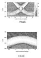
- the Figure 2A represents the calculated transmission in a component of the type of Figure 1A , in TM mode, with an azimuth of 0 ° relative to the grating vector, as a function of the angle of incidence ⁇ and the incident wavelength ⁇ .
- the angle of incidence ⁇ is the angle of incidence in the middle of the layer 103 defined with respect to the normal to the network.
- a software for calculating electromagnetic wave propagation is used, for example the software Gsolver ⁇ (developed by Grating Solver Development Company http://www.gsolver.com/ ).
- the corrugations have a sinusoidal profile with a pitch of 300 nm and a depth of 60 nm.
- the metal layer is silver and has a thickness of 40 nm.
- the centering wavelength is 560 nm.
- a spectral band typically 50 to 100 nm
- the coupling wavelength i.e., the wavelength at which there will be a resonant transmission effect by the component.
- Axial symmetry with respect to the y axis is observed around the 0 ° angle of incidence. The visual effect obtained will therefore be identical depending on whether we turn the sample in one direction or another.
- Simulations have also been carried out with different types of metals, varying the thickness. These calculations generally show a broadening of the coupling spectral band when the thickness of the metal layer decreases, with a lower resonant transmission amplitude when the thickness of the metal layer increases, the coupling spectral band is refined but loses in intensity. Thus, an optimum thickness of the metal layer can be calculated to have a significant visual effect with a sufficient coupling spectral band. For example, the applicant has shown that a silver metal layer is particularly advantageous, with a thickness of between 35 nm and 50 nm. Other metals have been tested. For example, aluminum can also be used to make a plasmon effect component according to the invention.
- the metal layer will have to be finer than that which one would have with silver, typically between 16 and 25 nm.
- the simulation of a structure with an aluminum metal layer has a coupling spectral band shifted towards the shorter wavelengths and a lower resonant transmission amplitude compared to the silver due to the higher Joule losses of the modes. of plasmon in this metal.
- the applicant has also studied the influence of the deformation of the sinusoidal profile of the corrugations on the efficiency of the coupling. It can be seen that changing the profile of a sinusoid towards a ripple profile having an unbalanced duty cycle causes a rapid drop in the transmission signal.
- the duty cycle can be between 40% and 60%.
- the Figure 2B represents a simulation of the transmission of the component 10 under conditions identical to the conditions of calculation of the Figure 2A but in which the sample was rotated in azimuth about the x-axis by 90 ° and selecting the TE polarization. At normal incidence, a resonant transmission at the centering wavelength ⁇ 0 is always observed. On the other hand, this curve shows stability of the coupling wavelength as a function of the angle of incidence. In other words, the component is insensitive in this configuration to the rotation of the sample around the y axis, now parallel to the network vector.
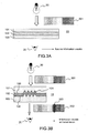
- the Figures 3B to 3D illustrate in 3 observation configurations of a security component 10 of the type of that of the figure 1 , the effect of the azimuth ⁇ and the angle of incidence or tilt ⁇ on the visual impression of an observer.
- the figure 3A illustrates as comparison the observation of a security component whose metal layer is not structured.
- the component 10 comprising an unstructured metal layer 102, arranged between two dielectric layers 101, 103, is illuminated by a light source 30, for example a white source whose spectrum is schematized by a set of colors symbolized by different dotted lines in the frame 301.
- a light source 30 for example a white source whose spectrum is schematized by a set of colors symbolized by different dotted lines in the frame 301.
- This is for example a spectrum covering all the visible light. If an observer observes the light transmitted through this component, he has no visual information. Indeed, there is no coupling with a plasmonic wave and the metal layer behaves like a reflector. The incident luminous flux is not transmitted by the component.
- a security component 10 is considered with a structured metal layer 102 to form a coupling zone 104 with corrugations, as previously described with reference to FIGS. Figures 1A and 1B .
- the observation is made for an azimuth of 0 ° and at normal incidence.
- the corrugations 104 form a coupling network of the incident wave with the surface plasmons supported by the metal-dielectric interfaces 105 and 106, optimized at normal incidence for a wavelength given by equation (3).
- the TM component of the incident electromagnetic wave is transmitted by the structure remarkably and an observer 20 observes a colored visual information corresponding to a fine spectral band around this wavelength.
- On the spectrum schematized by the frame 302 on the figure 3B only the light component 303 corresponding to this spectral band is visible to the observer.
- the observed component is rotated no longer along the y-axis perpendicular to the grating vector, but along the z-axis parallel to the grating vector.
- This configuration is indeed equivalent to the configuration illustrated on the Figure 2B wherein the component is rotated about an axis parallel to the grating vector.
- the component thus produced can be observed by an observer on one side or the other, that is to say in the example of Figures 3B to 3D presenting layer 101 or layer 103 to light source 30, with the same effects.
- the dielectric - metal - dielectric structure with the dielectric materials of similar or similar refractive indices is symmetrical, and the layers that could be added on both sides for the use of the component are neutral, as will be described later.
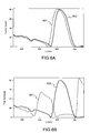
- the figure 4 represents an optical security component 40 according to an exemplary embodiment of the invention. This is a section at the level of the metal layer, only one of dielectric material layers being shown.
- the Figures 5A, 5B on the one hand, 6A, 6B on the other hand are figures or curves representing the calculated transmission of the component of the figure 4 according to different parameters.
- the component 40 comprises two coupling zones 41, 42, each comprising a set of corrugations 410, 420 symbolized by dotted bands on the figure 4 .
- the network vectors of each coupling zone are substantially orthogonal.
- the corrugations 410 of the coupling zone 41 are thus oriented along the z axis (network vector along the axis y), the undulations 420 of the coupling zone 42 are oriented along the y-axis (grating vector along the z-axis), the x-axis being the axis perpendicular to the surface of the component, which is also the plane of the Fig.
- the sets of corrugations 410, 420 have substantially identical characteristics (in particular the pitch and the nature of the metal), such that the centering wavelength is substantially identical for the two coupling zones.
- one of the parameters could be modified, for example the pitch of the corrugations, or the nature of the metal and the thickness of the layer, so as to have a centering wavelength and therefore a "color" at normal incidence different for an observer.
- the Figures 5A and 5B illustrate the transmission respectively calculated in the coupling zones 41 and 42, as a function of the angle of incidence measured around the z-axis and the wavelength, when an observer observes the component 40 with an azimuth of 0 ° in white light.
- the same electromagnetic wave propagation calculation software is used as above and the conditions are identical to those used for the simulations presented on the Figures 2A and 2B .
- the variation of the angle of incidence is made around an axis perpendicular to the grating vector.
- the simulation is performed in TM mode which the applicant has shown that the contribution was largely dominant compared to the contribution of the TE mode and therefore representative of what an observer will see in unpolarized light.
- the applicant has shown that a variation of 1 ° in angle introduces an offset of 7 nm for the polarization TM while the offset is almost zero in TE mode.
- an observer will see in transmission a green color corresponding to a spectral band centered on about 560 nm.
- the zone 41 By rotating the component around the z axis, it will see the zone 41 very quickly take a hue mainly made of red and a little blue, corresponding to the two coupling wavelengths linked to the co-propagative modes and contrapropagating.
- the rotation of the component along the z axis corresponds to a rotation along an axis parallel to the grating vector.
- the Figure 5B represents the variation of the transmission as a function of the angle of incidence and the wavelength calculated in TE mode, the contribution of which is in this largely dominant configuration compared to the TM mode.
- the color variation observed on the Figure 5B is much weaker and zone 42 will remain for the observer in green hues.
- the Figures 6A and 6B represent for an angle of incidence around the z axis ( figure 4 ) of respectively 0 ° (curve 602) and 15 ° (curve 601) the transmission as a function of the wavelength respectively in the zones 42 ( Figure 6A ) and 41 ( Figure 6B ), calculated with the same parameters as before. These curves confirm the small variation of the transmission as a function of the wavelength observed in the zone 42 with respect to the very strong variation of wavelength observed in the zone 41.
- the central wavelength of the Transmitted spectral band changes from 615 nm at normal incidence, at 601 nm at an angle of 15 ° in zone 42, while it goes from 615 nm at normal incidence, to 508 nm at an angle of 15 ° in zone 41. .
- the orthogonality of the coupling networks formed by the sets of corrugations 410 and 420 is respected at ⁇ 5 °.
- the applicant has indeed demonstrated that in this range of variation of the angle between the two sets of corrugations, one continues to perceive a very good color stability of the coupling zone whose vector grating is parallel to the axis of rotation of the component and an equally effective variation of the coupling wavelength in the coupling area whose grating vector is perpendicular to the axis of rotation of the component. If the orthogonality of the two sets of ripples deviates beyond the threshold by approximately ⁇ 5 °, the effect will be less and less visible, since the contrast between the color stable coupling zone and the color fast coupling will be less.
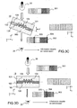
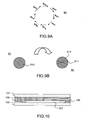
- FIG. 7A is a sectional view of an example of a safety component 70, at the level of the metal layer 102.
- Figures 7B to 7D illustrate the observation of the component 70 in transmission in different configurations.
- a coupling region 72 comprising a set of rectilinear and parallel corrugations forming a network vector coupling network k g2 has a core shape.
- the coupling zone 71 comprises substantially rectilinear and parallel corrugations, arranged in a direction perpendicular to that of the corrugations of the coupling zone 72 to form a network vector coupling network k g1 and its shape is complementary to that of the In this example, the coupling zone 71 has a substantially rectangular shape with an interruption of the corrugations in a central zone corresponding to the coupling zone 72.
- the security component represented on the FIG. Figure 7A comprises a zone 73 which forms a frame around the coupling zone 71 and in which the metal layer is not structured.
- the safety component 70 in normal incidence transmission, he will see an image of the type represented on the Figure 7B that is to say of uniform color over the entire component (if the parameters of the sets of corrugations are substantially identical) except on the unstructured zone 73, which has a constant optical density that is substantially higher than those of the structured areas 71, 72.
- the color will be that corresponding to a spectral band centered on the wavelength for which the network formed of the corrugations is optimized, for example a green color around 550 nm, as in the previous example .
- An observer can easily verify the authenticity of a secure document of value with such a component, and at different levels of security. It will be enough for him to observe in nonpolarized white light the component in transmission. By varying the angle of observation of the component in tilt around one of the axes of the pattern, it will observe a rapid variation of the color in a zone. This variation will be all the more characteristic that in a complementary zone, the color will vary very little. Moreover, the presence of an unstructured reference area (zone 73 in the example of the figure 7 ) and therefore opaque, will highlight the transparency of the coupling areas. For a second level of verification, it can vary the angle of incidence of the component around an axis perpendicular to the first axis. He will observe then a fast variation of the color in the zone complementary to the first one.
- the figures 8 and 9 illustrate two variants of a security component according to the invention with coupling areas whose network vectors are perpendicular two by two.
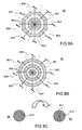
- the Figures 8A and 8B illustrate safety components with 800 waves arranged concentrically.
- the corrugations 800 may have polygonal shapes ( figure 8A ) or circulars ( Figure 8B ). It is possible to define a plurality of coupling zones referenced 801 to 808 in each of which portions of corrugations are substantially rectilinear and parallel forming a coupling network defined by a network vector k g1 to k g8 .
- FIG. 9A schematically shows a safety component 90 also axially symmetrical, which would present radially arranged corrugations (not shown on the drawing).
- Figure 9A so that locally it is possible to define coupling zones in which the corrugations are substantially rectilinear and linear, defining in each zone a grating vector k gi of direction perpendicular to the main direction of the corrugations of the zone.
- the security components as described above can be implemented as follows.
- the optical structures (corrugations) of the different zones are recorded by photolithography or electron beam lithography on a photosensitive support or "photoresist” according to the Anglo-Saxon expression.
- An electroplating step allows to postpone these optical structures in a resistant material for example based on nickel to make the matrix or "master”.
- Embossing is performed from the die to transfer the microstructure to a film and structure the layer of dielectric material 101 ( Figure 1A ), typically a stamping varnish of a few microns thick carried by a film of 12 microns to 50 microns in polymer material, for example PET (polyethylene terephthalate).
- the stamping can be done by hot pressing the dielectric material ("hot embossing") or by casting ("casting").
- the refractive index of the layer formed of the stamping varnish is typically 1.5.
- the metallization is done under vacuum, in a perfectly controlled manner in thickness, with, for example, the following metals: silver, aluminum, gold, chromium, copper, etc.
- a controlled refractive index closure layer is then applied, for example by a coating method. For some applications, such as rolling or hot stamping products, this layer may be the adhesive layer.
- the closure layer which forms layer 103 ( Figure 1A ) has a refractive index substantially the same as that of the embossed layer, around 1.5, with a thickness greater than several microns.
- an adhesive may be applied to the closure layer.
- the metallization step it is possible at the time of the metallization step to apply several different metals, for example to look for different visual effects.
- a second selective metallization is carried out also comprising a preliminary printing step of soluble ink for selecting the application areas of the second metal. It is possible during the application of the second metal that the metal layers are superimposed locally, forming zones of greater optical density, or on the contrary that results in non-metallized zones which, once closed by the closure layer , will form transparent areas in the component.
- the different metal zones may correspond to different coupling zones.
- the first metal is applied to one or more first coupling zone (s), while the second metal is applied to one or more other second coupling zone (s), allowing in the different coupling areas of distinct colored effects.
- the different metals can be deposited in zones that do not correspond to the coupling zones.
- the more opaque areas that require at least 2 metallizations or on the contrary, more transparent that can exist from the first partial metallization, can be exploited to form graphical elements of separation between the formed zones of different metals. These elements will be used by those skilled in the art to enhance the strength of the design and therefore a better readability for the person in charge of control.
- the figure 10 schematically represents a (partial) sectional view of the component thus obtained. Only the functional layers are shown in this figure for obtaining the plasmonic effect. Any support or adhesive films are not shown. Between the layers 101 and 103 of dielectric material, are the two metal layers 108, 109. The zone 107 represents the zone where the layer 103 is embossed and the structured metal layers, that is to say the zone where are the undulations (not shown). According to one variant, the different metals may correspond to different coupling zones. Due to the different nature of the metals used, such a component may have different color effects depending on the areas as well when one observes the color reflected by the material as during the transmission observation of the plasmonic waves. Indeed, the "plasmonic" color of a network results from the network and the nature of the metal layer. Moreover, the implementation being more complex, such a product has a potential resistance to counterfeiting much higher.
- an optical security component according to the invention in a secure document is perfectly compatible with the presence in the same document of structures based on networks commonly used for the production of holographic components.
- a security optical element comprising one or more plasmon-type components as described above and one or more other type of optical security components, for example of the holographic type.
- a matrix may be made by recording the different patterns corresponding to the different optical security components on the photoresist support and electroplating. The stamping can then be performed from the matrix to transfer the different microstructures on the film of polymer material for embossing.
- Metallization whose thickness must be controlled for the effect components Plasmonia can be made on the entire film because it will not interfere with other DOVID components operating in reflection.
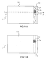
- the Figures 11A to 11C represent a secure document 1, for example a banknote-type value document, thus equipped with a security element 110 comprising a plasmon-type security optical component 70 and other security optical components 111, for example holographic type.
- the figure 11A represents a view from above of this component
- the Figure 11B represents a view from below
- the figure 11C a sectional view.
- the security element 110 is in the form of a strip, typically of width 15 mm which is fixed on a support 112 of the document 1.
- the security element 110 is fixed to the support 112 by known means.
- the security element can be attached by hot transfer reactivating a transparent adhesive layer previously applied to the closure layer 101.
- a release layer for example a wax
- the security element is transferred to the document by hot pressing the security element on the document, the plasmonic component being in front of the transparent zone.
- the adhesive film sticks on the support 112 of the document and the release layer and the support film are removed.
- a transparency window 113 at the level of the plasmonic type component 70.
- all the optical security components will be visible on the secure document 1 and controllable in reflection according to the various methods known in the art prior. Viewed from below, only the plasmon-type component (s) will be visible; they can be controlled in transmission, as described above.
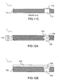
- FIGS. 12A and 12B illustrate by sectional views two variants of an exemplary embodiment of a secure document 1 equipped with a security element comprising a security optical component 120.
- the optical security component or the element optical security supporting the security optical component, is encapsulated in the support 122 of the secure document.
- the secure document 1 is for example obtained by rolling several layers 125, 126, 127, the security optical component being integrated in the layer 126 of the medium, while zones of transparency 123, 124 are provided in the outer layers 123, 124 to provide transparency observation of the security optical component 120.
- the layers 125, 126, 127 may be fused to form a homogeneous support 122 wherein the security optical component is encapsulated.
- the security optical component is fixed on a first layer 122 forming a support, the assembly being covered with a layer of transparent material 124.
- a transparency window 123 is provided in the support layer 122 to ensure the observation in transparency of the security optical component 120.
- This transparency window may be formed of vacuum or of a locally transparent material.
- the document 1 thus produced is for example a security document such as an identity card or a bank note provided with its security thread.
- the plasmon-type optical security component according to the invention can be presented as a security film whose characteristics can be controlled visually in the eye. Visual authentication of the secure document is therefore possible, including in natural light. This authentication, based on visual effects in different transmission depending on the axis of rotation of the component, is particularly easy to achieve.
- an observer can control the secure document by observing in transmission the plasmon-type component in front of a white light source.
- we can control the security component by placing it on a light support.
- the security optical component according to the invention and the method of manufacturing said component comprise various variants, modifications and improvements which will be obvious to those skilled in the art. it being understood that these various variants, modifications and improvements fall within the scope of the invention as defined by the following claims.
Landscapes
- Physics & Mathematics (AREA)
- General Physics & Mathematics (AREA)
- Optics & Photonics (AREA)
- Accounting & Taxation (AREA)
- Business, Economics & Management (AREA)
- Finance (AREA)
- Computer Security & Cryptography (AREA)
- Engineering & Computer Science (AREA)
- Credit Cards Or The Like (AREA)
- Laminated Bodies (AREA)
- Optical Elements Other Than Lenses (AREA)
- Optical Integrated Circuits (AREA)
- Diffracting Gratings Or Hologram Optical Elements (AREA)
- Optical Filters (AREA)
Claims (20)
- Optische Sicherheitskomponente mit Plasmonen-Wirkung, die dazu bestimmt ist, in Durchsicht beobachtet zu werden, umfassend:- zwei Schichten (101, 103) aus transparentem dielektrischen Material,- eine Metallschicht (102), die zwischen den Schichten aus transparentem dielektrischen Material angeordnet ist, um zwei Metall-Dielektrikum-Grenzflächen (105, 106) zu bilden, dadurch gekennzeichnet, dass die Metallschicht strukturiert ist, um mindestens auf einem Teil ihrer Oberfläche Wellen (104) zu bilden, die geeignet sind, Oberflächenplasmonenmoden, die durch die Metall-Dielektrikum-Grenzflächen getragen sind, mit einer einfallenden Lichtwelle zu koppeln, wobei die Wellen in einem ersten Kopplungsbereich entlang einer ersten Hauptrichtung und in mindestens einem zweiten Kopplungsbereich, der sich von dem ersten Kopplungsbereich unterscheidet, entlang einer zweiten Hauptrichtung, die im Wesentlichen senkrecht zu der ersten Hauptrichtung ist, angeordnet sind, wobei die Metallschicht auf jedem der Kopplungsbereiche durchgehend ist.
- Optische Sicherheitskomponente gemäß Anspruch 1, wobei die zwei Kopplungsbereiche komplementäre Muster (71, 72) bilden.
- Optische Sicherheitskomponente gemäß Anspruch 1, wobei mindestens ein Teil der Wellen konzentrisch angeordnet ist.
- Optische Sicherheitskomponente gemäß Anspruch 1, wobei mindestens ein Teil der Wellen radial angeordnet ist.
- Optische Sicherheitskomponente gemäß einem der vorhergehenden Ansprüche, wobei die Metallschicht außerdem einen nicht strukturierten Bereich aufweist.
- Optische Sicherheitskomponente gemäß einem der vorhergehenden Ansprüche, wobei die Wellen eine Länge, die zwischen 100 nm und 600 nm beträgt, und eine Tiefe, die zwischen 10 % und 30 % der Länge beträgt, aufweisen.
- Optische Sicherheitskomponente gemäß einem der vorhergehenden Ansprüche, wobei die Brechungsindexdifferenz der transparenten dielektrischen Materialien, die jeweils die Schichten bilden, niedriger als 0,1 ist,
- Optische Sicherheitskomponente gemäß einem der vorhergehenden Ansprüche, wobei mindestens ein Teil der Metallschicht aus Silber gebildet ist und seine Dicke im Wesentlichen zwischen 20 und 60 mm beträgt.
- Optische Sicherheitskomponente gemäß einem der vorhergehenden Ansprüche, wobei mindestens ein Bereich der Metallschicht aus Aluminium gebildet ist und seine Dicke im Wesentlichen zwischen 10 und 30 mm beträgt.
- Optische Sicherheitskomponente gemäß einem der vorhergehenden Ansprüche, wobei die Metallschicht aus einem einzigen Metall gebildet ist.
- Optische Sicherheitskomponente gemäß einem der Ansprüche 1 bis 9, wobei die Metallschicht mindestens zwei Teile aufweist, die jeweils aus einem unterschiedlichen Metall gebildet sind.
- Optisches Sicherheitselement, das zur Sicherung eines Dokuments bestimmt ist und mindestens eine optische Sicherheitskomponente gemäß einem der vorhergehenden Ansprüche aufweist.
- Optisches Sicherheitselement gemäß Anspruch 12, umfassend außerdem eine Trägerfolie, die eine der Schichten aus transparentem dielektrischen Material trägt.
- Optisches Sicherheitselement gemäß einem der Ansprüche 12 oder 13, umfassend außerdem eine Klebfolie, die auf einer der Schichten aus transparentem dielektrischen Material angeordnet ist.
- Sicherheitsdokument (1), umfassend einen Träger (112) und eine optische Sicherheitskomponente gemäß einem der Ansprüche 1 bis 11 oder ein optisches Sicherheitselement gemäß einem der Ansprüche 12 bis 14, das auf dem Träger befestigt ist, wobei der Träger einen Transparenzbereich (113) aufweist, an dem die optische Sicherheitskomponente angeordnet ist.
- Sicherheitsdokument (1), umfassend einen Träger (122) und eine optische Sicherheitskomponente gemäß einem der Ansprüche 1 bis 11 oder ein optisches Sicherheitselement gemäß einem der Ansprüche 12 bis 14, das in dem Träger eingekapselt ist, wobei der Träger Transparenzbereiche (123, 124) auf beiden Seiten der optischen Sicherheitskomponente aufweist.
- Verfahren zur Herstellung einer optischen Sicherheitskomponente mit Plasmonen-Wirkung, umfassend:- das Auftragen einer Metallschicht auf eine erste Schicht (103) aus transparentem dielektrischen Material,- das Einkapseln der Metallschicht durch eine zweite Schicht (101) aus dielektrischem Material, um zwei Metall-Dielektrikum- Grenzflächen (105, 106) zu bilden,wobei das Verfahren dadurch gekennzeichnet ist, dass die Metallschicht strukturiert wird, um mindestens auf einem Teil ihrer Oberfläche Wellen (104) zu bilden, die geeignet sind, Oberflächenplasmonenmoden, die durch die Metall-Dielektrikum-Grenzflächen getragen sind, mit einer einfallenden Lichtwelle zu koppeln, wobei die Wellen in einem ersten Kopplungsbereich entlang einer ersten Hauptrichtung und in mindestens einem zweiten Kopplungsbereich, der sich von dem ersten Kopplungsbereich unterscheidet, entlang einer zweiten Hauptrichtung, die im Wesentlichen senkrecht zu der ersten Hauptrichtung ist, angeordnet werden, wobei die Metallschicht auf jedem der Kopplungsbereiche durchgehend ist.
- Verfahren gemäß Anspruch 17, wobei die erste Schicht aus dielektrischem Material strukturiert wird, um die Wellen zu bilden, und die Metallschicht mit einer Dicke aufgetragen wird, die im Wesentlichen konstant auf der ersten Schicht ist, die auf diese Weise strukturiert wird.
- Verfahren gemäß Anspruch 18, wobei das Auftragen der Metallschicht das Auftragen einer ersten Schicht (108), die ein erstes Metall auf einen ersten Abschnitt der Oberfläche der ersten Schicht (103) aus dielektrischem Material aufweist, und das Auftragen von mindestens einer zweiten Schicht (109) aufweist, die ein zweites Metall auf einen zweiten Abschnitt der Oberfläche der ersten Schicht (103) aus dielektrischem Material aufweist.
- Verfahren gemäß den Ansprüchen 17 bis 19, wobei das Auftragen der Metallschicht selektiv vorgenommen wird, um makroskopische Muster definieren zu können, die in Durchsicht mit bloßem Auge sichtbar sind.
Applications Claiming Priority (2)
| Application Number | Priority Date | Filing Date | Title |
|---|---|---|---|
| FR1153068A FR2973917B1 (fr) | 2011-04-08 | 2011-04-08 | Composant optique de securite a effet transmissif, fabrication d'un tel composant et document securise equipe d'un tel composant |
| PCT/EP2012/056301 WO2012136777A1 (fr) | 2011-04-08 | 2012-04-05 | Composant optique de securite a effet transmissif, fabrication d'un tel composant et document securisé equipé d'un tel composant |
Publications (3)
| Publication Number | Publication Date |
|---|---|
| EP2695006A1 EP2695006A1 (de) | 2014-02-12 |
| EP2695006B1 true EP2695006B1 (de) | 2015-10-14 |
| EP2695006B2 EP2695006B2 (de) | 2022-04-06 |
Family
ID=45999796
Family Applications (1)
| Application Number | Title | Priority Date | Filing Date |
|---|---|---|---|
| EP12716306.1A Active EP2695006B2 (de) | 2011-04-08 | 2012-04-05 | Optische sicherheitskomponente mit einem durchlässigen effekt, herstellung einer derartigen komponente und sicheres dokument mit einer solchen komponente |
Country Status (10)
| Country | Link |
|---|---|
| US (1) | US9744793B2 (de) |
| EP (1) | EP2695006B2 (de) |
| CN (1) | CN103597380B (de) |
| AU (1) | AU2012238590B2 (de) |
| BR (1) | BR112013025971B1 (de) |
| CA (1) | CA2832477C (de) |
| FR (1) | FR2973917B1 (de) |
| MX (1) | MX2013011651A (de) |
| UA (1) | UA110968C2 (de) |
| WO (1) | WO2012136777A1 (de) |
Families Citing this family (33)
| Publication number | Priority date | Publication date | Assignee | Title |
|---|---|---|---|---|
| CN103081134B (zh) * | 2010-08-24 | 2015-08-19 | 日本电气株式会社 | 光源与投影型显示设备 |
| GB2493698B (en) * | 2011-08-08 | 2018-02-28 | Univ Nottingham Trent | Surface plasmon resonance in thin films |
| FR2982038B1 (fr) * | 2011-10-28 | 2013-11-15 | Hologram Ind | Composant optique de securite a effet reflectif, fabrication d'un tel composant et document securise equipe d'un tel composant |
| DE102012108169A1 (de) | 2012-09-03 | 2014-05-28 | Ovd Kinegram Ag | Sicherheitselement sowie Sicherheitsdokument |
| FR2996338B1 (fr) * | 2012-09-28 | 2020-10-16 | Hologram Ind | Composant optique de securite a effet reflectif, fabrication d'un tel composant et document securise equipe d'un tel composant |
| DE102012110630A1 (de) | 2012-11-06 | 2014-05-08 | Ovd Kinegram Ag | Mehrschichtkörper sowie Verfahren zur Herstellung eines Sicherheitselements |
| EP3427968B2 (de) | 2013-03-12 | 2023-03-01 | Toppan Printing Co., Ltd. | Darstellung |
| FR3017231B1 (fr) * | 2014-01-31 | 2020-07-24 | Hologram Ind | Composant optique de securite a effet plasmonique, fabrication d'un tel composant et document securise equipe d'un tel composant |
| JP6645422B2 (ja) | 2014-03-27 | 2020-02-14 | 凸版印刷株式会社 | 表示体、および、表示体の観察方法 |
| US11126902B2 (en) | 2014-06-03 | 2021-09-21 | IE-9 Technology Corp. | Optically variable data storage device |
| US9489604B2 (en) | 2014-06-03 | 2016-11-08 | IE-9 Technology Corp. | Optically variable data storage device |
| DE102014010751A1 (de) | 2014-07-21 | 2016-01-21 | Giesecke & Devrient Gmbh | Sicherheitselement mit Subwellenlängengitter |
| DE102015010191A1 (de) | 2015-08-06 | 2017-02-09 | Giesecke & Devrient Gmbh | Sicherheitselement mit Subwellenlängengitter |
| FR3040015B1 (fr) * | 2015-08-11 | 2017-09-08 | Hologram Ind | Composant optique de securite a effet plasmonique et procede de fabrication d'un tel composant |
| CN105353432B (zh) * | 2015-11-18 | 2016-08-17 | 武汉大学 | 一种实时动态等离激元调控变色的机械变色龙 |
| FR3051565B1 (fr) | 2016-05-23 | 2019-06-21 | Surys | Composant optique de securite et procede de fabrication d'un tel composant |
| WO2017204071A1 (ja) * | 2016-05-27 | 2017-11-30 | 大日本印刷株式会社 | 表示体、印刷物および情報記録媒体 |
| DE102016013690A1 (de) | 2016-11-16 | 2018-05-17 | Giesecke+Devrient Currency Technology Gmbh | Sicherheitselement mit Subwellenlängengitter |
| DE102016013683A1 (de) | 2016-11-16 | 2018-05-17 | Giesecke+Devrient Currency Technology Gmbh | Sicherheitselement mit Subwellenlängengitter |
| WO2019039572A1 (ja) * | 2017-08-23 | 2019-02-28 | 凸版印刷株式会社 | 表示体、偽造防止スレッド用紙、および偽造防止媒体 |
| FR3072053B1 (fr) | 2017-10-10 | 2019-11-08 | Surys | Composant optique de securite a effet reflectif, fabrication d'un tel composant et document securise equipe d'un tel composant |
| FR3072325B1 (fr) | 2017-10-10 | 2019-11-08 | Surys | Composant optique de securite visible en reflexion, fabrication d'un tel composant et document securise equipe d'un tel composant |
| CN107872458B (zh) * | 2017-11-10 | 2019-07-12 | 恒宝股份有限公司 | 一种芯片及其访问方法 |
| WO2019121798A1 (fr) | 2017-12-19 | 2019-06-27 | Surys | Composant optique de securite visible en reflexion, fabrication d'un tel composant et document securisé equipé d'un tel composant |
| DE102018003602A1 (de) * | 2018-05-03 | 2019-11-07 | Giesecke+Devrient Currency Technology Gmbh | Retroreflektierende Folie, Folie, Datenträger und Verwendung |
| TR201817901A2 (tr) | 2018-11-26 | 2020-06-22 | Atilim Ueniversitesi | İnce film yüzey renklendirme ile optik şifreleme ve şifre kırma yapısı. |
| EP3966619A4 (de) * | 2018-11-29 | 2022-12-07 | La Trobe University | Mikroskopieverfahren und -system |
| FR3095281B1 (fr) * | 2019-04-19 | 2021-08-27 | Horiba France Sas | Réseau de diffraction en réflexion résistant à un flux lumineux à impulsions ultra-courtes de forte puissance crête et son procédé de fabrication |
| FR3095981B1 (fr) | 2019-05-13 | 2021-06-04 | Surys | Composant optique de sécurité à effet plasmonique, fabrication d’un tel composant et objet sécurisé équipé d’un tel composant |
| KR20220063259A (ko) * | 2019-09-25 | 2022-05-17 | 도판 인사츠 가부시키가이샤 | 컬러 표시체, 인증 매체, 및 컬러 표시체의 진안 판정 방법 |
| WO2021151459A1 (en) | 2020-01-27 | 2021-08-05 | Orell Füssli AG | Security document with lightguide having a sparse outcoupler structure |
| FR3111843A1 (fr) | 2020-06-30 | 2021-12-31 | Surys | Procédés de fabrication de composants optiques de sécurité, composants optiques de sécurité et objets sécurisés équipés de tels composants |
| FR3144546A1 (fr) | 2022-12-30 | 2024-07-05 | Surys | Composants optiques de sécurité visibles en transmission, fabrication de tels composants et objets sécurisés équipés de tels composants |
Citations (11)
| Publication number | Priority date | Publication date | Assignee | Title |
|---|---|---|---|---|
| WO2001044839A1 (en) | 1999-12-17 | 2001-06-21 | Qinetiq Limited | Textured surface |
| US6428051B1 (en) | 1993-10-13 | 2002-08-06 | Leonhard Kurz Gmbh & Co. | Value-bearing document with window |
| WO2003059643A1 (de) | 2002-01-18 | 2003-07-24 | Ovd Kinegram Ag | Diffraktives sicherheitselement mit integriertem optischen wellenleiter |
| EP1801546A1 (de) | 2005-12-23 | 2007-06-27 | SICK STEGMANN GmbH | Informationsträger in einem Encoder |
| US20070200940A1 (en) | 2006-02-28 | 2007-08-30 | Gruhlke Russell W | Vertical tri-color sensor |
| WO2008031170A1 (en) | 2006-09-15 | 2008-03-20 | Securency International Pty Ltd | Radiation curable embossed ink security devices for security documents. |
| US20090190223A1 (en) | 2006-05-02 | 2009-07-30 | Valery Petiton | Optical security marking component, method of manufacturing such a component, system comprising such a component, and reader for checking such a component |
| WO2010063737A1 (en) | 2008-12-01 | 2010-06-10 | Optaglio, S.R.O. | Optical device and method of manufacture |
| EP2228671A1 (de) | 2009-03-11 | 2010-09-15 | Giesecke & Devrient GmbH | Sicherheitselement |
| EP2228672A1 (de) | 2009-03-11 | 2010-09-15 | Giesecke & Devrient GmbH | Sicherheitselement mit mehrfarbigem Bild |
| US20100307705A1 (en) | 2007-12-21 | 2010-12-09 | Giesecke & Devrient Gmbh | Security element |
-
2011
- 2011-04-08 FR FR1153068A patent/FR2973917B1/fr active Active
-
2012
- 2012-04-05 US US14/110,509 patent/US9744793B2/en active Active
- 2012-04-05 AU AU2012238590A patent/AU2012238590B2/en active Active
- 2012-04-05 CN CN201280027813.9A patent/CN103597380B/zh active Active
- 2012-04-05 WO PCT/EP2012/056301 patent/WO2012136777A1/fr active Application Filing
- 2012-04-05 EP EP12716306.1A patent/EP2695006B2/de active Active
- 2012-04-05 CA CA2832477A patent/CA2832477C/en active Active
- 2012-04-05 MX MX2013011651A patent/MX2013011651A/es active IP Right Grant
- 2012-04-05 BR BR112013025971-0A patent/BR112013025971B1/pt active IP Right Grant
- 2012-05-04 UA UAA201312953A patent/UA110968C2/uk unknown
Patent Citations (11)
| Publication number | Priority date | Publication date | Assignee | Title |
|---|---|---|---|---|
| US6428051B1 (en) | 1993-10-13 | 2002-08-06 | Leonhard Kurz Gmbh & Co. | Value-bearing document with window |
| WO2001044839A1 (en) | 1999-12-17 | 2001-06-21 | Qinetiq Limited | Textured surface |
| WO2003059643A1 (de) | 2002-01-18 | 2003-07-24 | Ovd Kinegram Ag | Diffraktives sicherheitselement mit integriertem optischen wellenleiter |
| EP1801546A1 (de) | 2005-12-23 | 2007-06-27 | SICK STEGMANN GmbH | Informationsträger in einem Encoder |
| US20070200940A1 (en) | 2006-02-28 | 2007-08-30 | Gruhlke Russell W | Vertical tri-color sensor |
| US20090190223A1 (en) | 2006-05-02 | 2009-07-30 | Valery Petiton | Optical security marking component, method of manufacturing such a component, system comprising such a component, and reader for checking such a component |
| WO2008031170A1 (en) | 2006-09-15 | 2008-03-20 | Securency International Pty Ltd | Radiation curable embossed ink security devices for security documents. |
| US20100307705A1 (en) | 2007-12-21 | 2010-12-09 | Giesecke & Devrient Gmbh | Security element |
| WO2010063737A1 (en) | 2008-12-01 | 2010-06-10 | Optaglio, S.R.O. | Optical device and method of manufacture |
| EP2228671A1 (de) | 2009-03-11 | 2010-09-15 | Giesecke & Devrient GmbH | Sicherheitselement |
| EP2228672A1 (de) | 2009-03-11 | 2010-09-15 | Giesecke & Devrient GmbH | Sicherheitselement mit mehrfarbigem Bild |
Non-Patent Citations (1)
| Title |
|---|
| JOURLIN ET AL.: "Spatially and polarization resolved plasmon mediated transmission through continuous metal films", OPTICS EXPRESS, vol. 17, no. 14, July 2009 (2009-07-01), pages 12155 - 12166, XP055296944 |
Also Published As
| Publication number | Publication date |
|---|---|
| US9744793B2 (en) | 2017-08-29 |
| US20140028012A1 (en) | 2014-01-30 |
| UA110968C2 (uk) | 2016-03-10 |
| WO2012136777A1 (fr) | 2012-10-11 |
| RU2013149797A (ru) | 2015-05-20 |
| EP2695006B2 (de) | 2022-04-06 |
| BR112013025971A2 (pt) | 2018-01-23 |
| EP2695006A1 (de) | 2014-02-12 |
| MX2013011651A (es) | 2014-02-17 |
| AU2012238590A8 (en) | 2013-11-21 |
| FR2973917B1 (fr) | 2014-01-10 |
| CA2832477A1 (en) | 2012-10-11 |
| CN103597380A (zh) | 2014-02-19 |
| FR2973917A1 (fr) | 2012-10-12 |
| AU2012238590A1 (en) | 2013-11-07 |
| BR112013025971B1 (pt) | 2020-10-13 |
| AU2012238590B2 (en) | 2015-05-28 |
| CN103597380B (zh) | 2016-02-03 |
| CA2832477C (en) | 2016-11-22 |
Similar Documents
| Publication | Publication Date | Title |
|---|---|---|
| EP2695006B1 (de) | Optische sicherheitskomponente mit einem durchlässigen effekt, herstellung einer derartigen komponente und sicheres dokument mit einer solchen komponente | |
| EP2771724B1 (de) | Optisches sicherheitskomponente mit reflektierender wirkung, herstellung dieser komponente und gesichertes dokument mit einer solchen komponente | |
| EP3099513B1 (de) | Plasmonische optische sicherheitskomponente, herstellung solch einer komponente und mit solch einer komponente ausgestattetes sicheres dokument | |
| EP3129238B1 (de) | Optische sicherheitskomponente mit reflektierender wirkung, herstellung solch einer komponente und sicheres dokument mit solch einer komponente | |
| EP3334611B1 (de) | Optisches sicherheitsbauelement mit plasmoneneffekt und verfahren zur herstellung solch einer komponente | |
| EP3634771B1 (de) | Optische, bei reflektion sichtbare sicherheitskomponente, herstellung solch einer komponente | |
| FR3051565B1 (fr) | Composant optique de securite et procede de fabrication d'un tel composant | |
| WO2014049108A1 (fr) | Composant optique de securite a effet reflectif, fabrication d'un tel composant et document securisé equipé d'un tel composant | |
| EP3969293B1 (de) | Optische sicherheitskomponente mit plasmonischem effekt, herstellung einer solchen komponente und sicheres dokument mit einer solchen komponente | |
| EP3727872B1 (de) | Optische, bei reflektion sichtbare sicherheitskomponente, herstellung solch einer komponente und sicheres dokument mit solch einer komponente | |
| WO2022214689A1 (fr) | Composants optiques de sécurité visibles en réflexion, fabrication de tels composants et documents sécurisés équipés de tels composants |
Legal Events
| Date | Code | Title | Description |
|---|---|---|---|
| PUAI | Public reference made under article 153(3) epc to a published international application that has entered the european phase |
Free format text: ORIGINAL CODE: 0009012 |
|
| 17P | Request for examination filed |
Effective date: 20131025 |
|
| AK | Designated contracting states |
Kind code of ref document: A1 Designated state(s): AL AT BE BG CH CY CZ DE DK EE ES FI FR GB GR HR HU IE IS IT LI LT LU LV MC MK MT NL NO PL PT RO RS SE SI SK SM TR |
|
| DAX | Request for extension of the european patent (deleted) | ||
| GRAP | Despatch of communication of intention to grant a patent |
Free format text: ORIGINAL CODE: EPIDOSNIGR1 |
|
| INTG | Intention to grant announced |
Effective date: 20150713 |
|
| GRAS | Grant fee paid |
Free format text: ORIGINAL CODE: EPIDOSNIGR3 |
|
| GRAA | (expected) grant |
Free format text: ORIGINAL CODE: 0009210 |
|
| STAA | Information on the status of an ep patent application or granted ep patent |
Free format text: STATUS: THE PATENT HAS BEEN GRANTED |
|
| AK | Designated contracting states |
Kind code of ref document: B1 Designated state(s): AL AT BE BG CH CY CZ DE DK EE ES FI FR GB GR HR HU IE IS IT LI LT LU LV MC MK MT NL NO PL PT RO RS SE SI SK SM TR |
|
| REG | Reference to a national code |
Ref country code: GB Ref legal event code: FG4D Free format text: NOT ENGLISH |
|
| REG | Reference to a national code |
Ref country code: AT Ref legal event code: REF Ref document number: 755562 Country of ref document: AT Kind code of ref document: T Effective date: 20151015 Ref country code: CH Ref legal event code: EP |
|
| REG | Reference to a national code |
Ref country code: IE Ref legal event code: FG4D Free format text: LANGUAGE OF EP DOCUMENT: FRENCH |
|
| REG | Reference to a national code |
Ref country code: DE Ref legal event code: R096 Ref document number: 602012011539 Country of ref document: DE |
|
| REG | Reference to a national code |
Ref country code: NL Ref legal event code: MP Effective date: 20151014 |
|
| REG | Reference to a national code |
Ref country code: LT Ref legal event code: MG4D |
|
| RAP2 | Party data changed (patent owner data changed or rights of a patent transferred) |
Owner name: SURYS Owner name: UNIVERSITE JEAN MONNET DE SAINT-ETIENNE |
|
| REG | Reference to a national code |
Ref country code: AT Ref legal event code: MK05 Ref document number: 755562 Country of ref document: AT Kind code of ref document: T Effective date: 20151014 |
|
| REG | Reference to a national code |
Ref country code: FR Ref legal event code: PLFP Year of fee payment: 5 |
|
| PG25 | Lapsed in a contracting state [announced via postgrant information from national office to epo] |
Ref country code: NO Free format text: LAPSE BECAUSE OF FAILURE TO SUBMIT A TRANSLATION OF THE DESCRIPTION OR TO PAY THE FEE WITHIN THE PRESCRIBED TIME-LIMIT Effective date: 20160114 Ref country code: HR Free format text: LAPSE BECAUSE OF FAILURE TO SUBMIT A TRANSLATION OF THE DESCRIPTION OR TO PAY THE FEE WITHIN THE PRESCRIBED TIME-LIMIT Effective date: 20151014 Ref country code: NL Free format text: LAPSE BECAUSE OF FAILURE TO SUBMIT A TRANSLATION OF THE DESCRIPTION OR TO PAY THE FEE WITHIN THE PRESCRIBED TIME-LIMIT Effective date: 20151014 Ref country code: ES Free format text: LAPSE BECAUSE OF FAILURE TO SUBMIT A TRANSLATION OF THE DESCRIPTION OR TO PAY THE FEE WITHIN THE PRESCRIBED TIME-LIMIT Effective date: 20151014 Ref country code: IS Free format text: LAPSE BECAUSE OF FAILURE TO SUBMIT A TRANSLATION OF THE DESCRIPTION OR TO PAY THE FEE WITHIN THE PRESCRIBED TIME-LIMIT Effective date: 20160214 Ref country code: LT Free format text: LAPSE BECAUSE OF FAILURE TO SUBMIT A TRANSLATION OF THE DESCRIPTION OR TO PAY THE FEE WITHIN THE PRESCRIBED TIME-LIMIT Effective date: 20151014 |
|
| PG25 | Lapsed in a contracting state [announced via postgrant information from national office to epo] |
Ref country code: PL Free format text: LAPSE BECAUSE OF FAILURE TO SUBMIT A TRANSLATION OF THE DESCRIPTION OR TO PAY THE FEE WITHIN THE PRESCRIBED TIME-LIMIT Effective date: 20151014 Ref country code: FI Free format text: LAPSE BECAUSE OF FAILURE TO SUBMIT A TRANSLATION OF THE DESCRIPTION OR TO PAY THE FEE WITHIN THE PRESCRIBED TIME-LIMIT Effective date: 20151014 Ref country code: SE Free format text: LAPSE BECAUSE OF FAILURE TO SUBMIT A TRANSLATION OF THE DESCRIPTION OR TO PAY THE FEE WITHIN THE PRESCRIBED TIME-LIMIT Effective date: 20151014 Ref country code: RS Free format text: LAPSE BECAUSE OF FAILURE TO SUBMIT A TRANSLATION OF THE DESCRIPTION OR TO PAY THE FEE WITHIN THE PRESCRIBED TIME-LIMIT Effective date: 20151014 Ref country code: GR Free format text: LAPSE BECAUSE OF FAILURE TO SUBMIT A TRANSLATION OF THE DESCRIPTION OR TO PAY THE FEE WITHIN THE PRESCRIBED TIME-LIMIT Effective date: 20160115 Ref country code: PT Free format text: LAPSE BECAUSE OF FAILURE TO SUBMIT A TRANSLATION OF THE DESCRIPTION OR TO PAY THE FEE WITHIN THE PRESCRIBED TIME-LIMIT Effective date: 20160215 Ref country code: AT Free format text: LAPSE BECAUSE OF FAILURE TO SUBMIT A TRANSLATION OF THE DESCRIPTION OR TO PAY THE FEE WITHIN THE PRESCRIBED TIME-LIMIT Effective date: 20151014 Ref country code: LV Free format text: LAPSE BECAUSE OF FAILURE TO SUBMIT A TRANSLATION OF THE DESCRIPTION OR TO PAY THE FEE WITHIN THE PRESCRIBED TIME-LIMIT Effective date: 20151014 |
|
| REG | Reference to a national code |
Ref country code: DE Ref legal event code: R026 Ref document number: 602012011539 Country of ref document: DE |
|
| PLBI | Opposition filed |
Free format text: ORIGINAL CODE: 0009260 |
|
| PLAX | Notice of opposition and request to file observation + time limit sent |
Free format text: ORIGINAL CODE: EPIDOSNOBS2 |
|
| 26 | Opposition filed |
Opponent name: GIESECKE & DEVRIENT GMBH Effective date: 20160713 |
|
| PG25 | Lapsed in a contracting state [announced via postgrant information from national office to epo] |
Ref country code: BE Free format text: LAPSE BECAUSE OF NON-PAYMENT OF DUE FEES Effective date: 20160430 Ref country code: EE Free format text: LAPSE BECAUSE OF FAILURE TO SUBMIT A TRANSLATION OF THE DESCRIPTION OR TO PAY THE FEE WITHIN THE PRESCRIBED TIME-LIMIT Effective date: 20151014 Ref country code: SK Free format text: LAPSE BECAUSE OF FAILURE TO SUBMIT A TRANSLATION OF THE DESCRIPTION OR TO PAY THE FEE WITHIN THE PRESCRIBED TIME-LIMIT Effective date: 20151014 Ref country code: SM Free format text: LAPSE BECAUSE OF FAILURE TO SUBMIT A TRANSLATION OF THE DESCRIPTION OR TO PAY THE FEE WITHIN THE PRESCRIBED TIME-LIMIT Effective date: 20151014 Ref country code: RO Free format text: LAPSE BECAUSE OF FAILURE TO SUBMIT A TRANSLATION OF THE DESCRIPTION OR TO PAY THE FEE WITHIN THE PRESCRIBED TIME-LIMIT Effective date: 20151014 Ref country code: DK Free format text: LAPSE BECAUSE OF FAILURE TO SUBMIT A TRANSLATION OF THE DESCRIPTION OR TO PAY THE FEE WITHIN THE PRESCRIBED TIME-LIMIT Effective date: 20151014 |
|
| PG25 | Lapsed in a contracting state [announced via postgrant information from national office to epo] |
Ref country code: SI Free format text: LAPSE BECAUSE OF FAILURE TO SUBMIT A TRANSLATION OF THE DESCRIPTION OR TO PAY THE FEE WITHIN THE PRESCRIBED TIME-LIMIT Effective date: 20151014 |
|
| PLBB | Reply of patent proprietor to notice(s) of opposition received |
Free format text: ORIGINAL CODE: EPIDOSNOBS3 |
|
| PG25 | Lapsed in a contracting state [announced via postgrant information from national office to epo] |
Ref country code: LU Free format text: LAPSE BECAUSE OF FAILURE TO SUBMIT A TRANSLATION OF THE DESCRIPTION OR TO PAY THE FEE WITHIN THE PRESCRIBED TIME-LIMIT Effective date: 20160405 |
|
| REG | Reference to a national code |
Ref country code: IE Ref legal event code: MM4A |
|
| REG | Reference to a national code |
Ref country code: FR Ref legal event code: PLFP Year of fee payment: 6 |
|
| PG25 | Lapsed in a contracting state [announced via postgrant information from national office to epo] |
Ref country code: IE Free format text: LAPSE BECAUSE OF NON-PAYMENT OF DUE FEES Effective date: 20160405 |
|
| PLAB | Opposition data, opponent's data or that of the opponent's representative modified |
Free format text: ORIGINAL CODE: 0009299OPPO |
|
| R26 | Opposition filed (corrected) |
Opponent name: GIESECKE+DEVRIENT CURRENCY TECHNOLOGY GMBH Effective date: 20160713 |
|
| REG | Reference to a national code |
Ref country code: FR Ref legal event code: PLFP Year of fee payment: 7 |
|
| APAH | Appeal reference modified |
Free format text: ORIGINAL CODE: EPIDOSCREFNO |
|
| APBM | Appeal reference recorded |
Free format text: ORIGINAL CODE: EPIDOSNREFNO |
|
| APBP | Date of receipt of notice of appeal recorded |
Free format text: ORIGINAL CODE: EPIDOSNNOA2O |
|
| PG25 | Lapsed in a contracting state [announced via postgrant information from national office to epo] |
Ref country code: HU Free format text: LAPSE BECAUSE OF FAILURE TO SUBMIT A TRANSLATION OF THE DESCRIPTION OR TO PAY THE FEE WITHIN THE PRESCRIBED TIME-LIMIT; INVALID AB INITIO Effective date: 20120405 Ref country code: CY Free format text: LAPSE BECAUSE OF FAILURE TO SUBMIT A TRANSLATION OF THE DESCRIPTION OR TO PAY THE FEE WITHIN THE PRESCRIBED TIME-LIMIT Effective date: 20151014 |
|
| APBQ | Date of receipt of statement of grounds of appeal recorded |
Free format text: ORIGINAL CODE: EPIDOSNNOA3O |
|
| PG25 | Lapsed in a contracting state [announced via postgrant information from national office to epo] |
Ref country code: MT Free format text: LAPSE BECAUSE OF FAILURE TO SUBMIT A TRANSLATION OF THE DESCRIPTION OR TO PAY THE FEE WITHIN THE PRESCRIBED TIME-LIMIT Effective date: 20151014 Ref country code: MK Free format text: LAPSE BECAUSE OF FAILURE TO SUBMIT A TRANSLATION OF THE DESCRIPTION OR TO PAY THE FEE WITHIN THE PRESCRIBED TIME-LIMIT Effective date: 20151014 Ref country code: MC Free format text: LAPSE BECAUSE OF FAILURE TO SUBMIT A TRANSLATION OF THE DESCRIPTION OR TO PAY THE FEE WITHIN THE PRESCRIBED TIME-LIMIT Effective date: 20151014 |
|
| PG25 | Lapsed in a contracting state [announced via postgrant information from national office to epo] |
Ref country code: AL Free format text: LAPSE BECAUSE OF FAILURE TO SUBMIT A TRANSLATION OF THE DESCRIPTION OR TO PAY THE FEE WITHIN THE PRESCRIBED TIME-LIMIT Effective date: 20151014 |
|
| APBU | Appeal procedure closed |
Free format text: ORIGINAL CODE: EPIDOSNNOA9O |
|
| PUAH | Patent maintained in amended form |
Free format text: ORIGINAL CODE: 0009272 |
|
| STAA | Information on the status of an ep patent application or granted ep patent |
Free format text: STATUS: PATENT MAINTAINED AS AMENDED |
|
| 27A | Patent maintained in amended form |
Effective date: 20220406 |
|
| AK | Designated contracting states |
Kind code of ref document: B2 Designated state(s): AL AT BE BG CH CY CZ DE DK EE ES FI FR GB GR HR HU IE IS IT LI LT LU LV MC MK MT NL NO PL PT RO RS SE SI SK SM TR |
|
| REG | Reference to a national code |
Ref country code: DE Ref legal event code: R102 Ref document number: 602012011539 Country of ref document: DE |
|
| PGFP | Annual fee paid to national office [announced via postgrant information from national office to epo] |
Ref country code: CZ Payment date: 20240326 Year of fee payment: 13 Ref country code: BG Payment date: 20240326 Year of fee payment: 13 Ref country code: GB Payment date: 20240320 Year of fee payment: 13 |
|
| PGFP | Annual fee paid to national office [announced via postgrant information from national office to epo] |
Ref country code: TR Payment date: 20240326 Year of fee payment: 13 Ref country code: IT Payment date: 20240320 Year of fee payment: 13 Ref country code: FR Payment date: 20240320 Year of fee payment: 13 |
|
| PGFP | Annual fee paid to national office [announced via postgrant information from national office to epo] |
Ref country code: DE Payment date: 20240320 Year of fee payment: 13 |
|
| PGFP | Annual fee paid to national office [announced via postgrant information from national office to epo] |
Ref country code: CH Payment date: 20240501 Year of fee payment: 13 |