EP2692896A1 - Mask for deposition and method for aligning the same - Google Patents
Mask for deposition and method for aligning the same Download PDFInfo
- Publication number
- EP2692896A1 EP2692896A1 EP20130178356 EP13178356A EP2692896A1 EP 2692896 A1 EP2692896 A1 EP 2692896A1 EP 20130178356 EP20130178356 EP 20130178356 EP 13178356 A EP13178356 A EP 13178356A EP 2692896 A1 EP2692896 A1 EP 2692896A1
- Authority
- EP
- European Patent Office
- Prior art keywords
- mask
- alignment mark
- deposition
- region
- substrate
- Prior art date
- Legal status (The legal status is an assumption and is not a legal conclusion. Google has not performed a legal analysis and makes no representation as to the accuracy of the status listed.)
- Withdrawn
Links
- 230000008021 deposition Effects 0.000 title claims abstract description 71
- 238000000034 method Methods 0.000 title claims description 24
- 239000000758 substrate Substances 0.000 claims abstract description 104
- 239000000463 material Substances 0.000 claims description 12
- 238000005530 etching Methods 0.000 claims description 3
- 230000000063 preceeding effect Effects 0.000 claims 3
- 238000004519 manufacturing process Methods 0.000 abstract description 3
- 230000002950 deficient Effects 0.000 abstract description 2
- 238000000151 deposition Methods 0.000 description 57
- 230000000052 comparative effect Effects 0.000 description 5
- 239000010408 film Substances 0.000 description 5
- 238000002347 injection Methods 0.000 description 4
- 239000007924 injection Substances 0.000 description 4
- 238000001771 vacuum deposition Methods 0.000 description 4
- 238000005259 measurement Methods 0.000 description 3
- 239000002184 metal Substances 0.000 description 3
- 229910052751 metal Inorganic materials 0.000 description 3
- 239000011368 organic material Substances 0.000 description 3
- 230000000149 penetrating effect Effects 0.000 description 3
- 239000010409 thin film Substances 0.000 description 3
- 230000004888 barrier function Effects 0.000 description 2
- 238000005137 deposition process Methods 0.000 description 2
- 238000010586 diagram Methods 0.000 description 2
- 230000005525 hole transport Effects 0.000 description 2
- 239000002245 particle Substances 0.000 description 2
- 239000000956 alloy Substances 0.000 description 1
- 229910045601 alloy Inorganic materials 0.000 description 1
- 239000003086 colorant Substances 0.000 description 1
- 238000005520 cutting process Methods 0.000 description 1
- 238000009826 distribution Methods 0.000 description 1
- 230000000694 effects Effects 0.000 description 1
- 238000005516 engineering process Methods 0.000 description 1
- 238000001704 evaporation Methods 0.000 description 1
- 230000007717 exclusion Effects 0.000 description 1
- 229920001002 functional polymer Polymers 0.000 description 1
- 230000005484 gravity Effects 0.000 description 1
- 230000005283 ground state Effects 0.000 description 1
- 238000007641 inkjet printing Methods 0.000 description 1
- 239000007769 metal material Substances 0.000 description 1
- 150000002739 metals Chemical class 0.000 description 1
- 239000000203 mixture Substances 0.000 description 1
- 238000012986 modification Methods 0.000 description 1
- 230000004048 modification Effects 0.000 description 1
- 238000000206 photolithography Methods 0.000 description 1
- 229920000642 polymer Polymers 0.000 description 1
- 230000036632 reaction speed Effects 0.000 description 1
- 238000005215 recombination Methods 0.000 description 1
- 230000006798 recombination Effects 0.000 description 1
- 239000004576 sand Substances 0.000 description 1
- 238000001179 sorption measurement Methods 0.000 description 1
- 238000004528 spin coating Methods 0.000 description 1
- 238000004544 sputter deposition Methods 0.000 description 1
Images




Classifications
-
- H—ELECTRICITY
- H10—SEMICONDUCTOR DEVICES; ELECTRIC SOLID-STATE DEVICES NOT OTHERWISE PROVIDED FOR
- H10K—ORGANIC ELECTRIC SOLID-STATE DEVICES
- H10K71/00—Manufacture or treatment specially adapted for the organic devices covered by this subclass
-
- B—PERFORMING OPERATIONS; TRANSPORTING
- B05—SPRAYING OR ATOMISING IN GENERAL; APPLYING FLUENT MATERIALS TO SURFACES, IN GENERAL
- B05C—APPARATUS FOR APPLYING FLUENT MATERIALS TO SURFACES, IN GENERAL
- B05C21/00—Accessories or implements for use in connection with applying liquids or other fluent materials to surfaces, not provided for in groups B05C1/00 - B05C19/00
- B05C21/005—Masking devices
-
- C—CHEMISTRY; METALLURGY
- C23—COATING METALLIC MATERIAL; COATING MATERIAL WITH METALLIC MATERIAL; CHEMICAL SURFACE TREATMENT; DIFFUSION TREATMENT OF METALLIC MATERIAL; COATING BY VACUUM EVAPORATION, BY SPUTTERING, BY ION IMPLANTATION OR BY CHEMICAL VAPOUR DEPOSITION, IN GENERAL; INHIBITING CORROSION OF METALLIC MATERIAL OR INCRUSTATION IN GENERAL
- C23C—COATING METALLIC MATERIAL; COATING MATERIAL WITH METALLIC MATERIAL; SURFACE TREATMENT OF METALLIC MATERIAL BY DIFFUSION INTO THE SURFACE, BY CHEMICAL CONVERSION OR SUBSTITUTION; COATING BY VACUUM EVAPORATION, BY SPUTTERING, BY ION IMPLANTATION OR BY CHEMICAL VAPOUR DEPOSITION, IN GENERAL
- C23C14/00—Coating by vacuum evaporation, by sputtering or by ion implantation of the coating forming material
- C23C14/04—Coating on selected surface areas, e.g. using masks
- C23C14/042—Coating on selected surface areas, e.g. using masks using masks
-
- H—ELECTRICITY
- H10—SEMICONDUCTOR DEVICES; ELECTRIC SOLID-STATE DEVICES NOT OTHERWISE PROVIDED FOR
- H10K—ORGANIC ELECTRIC SOLID-STATE DEVICES
- H10K71/00—Manufacture or treatment specially adapted for the organic devices covered by this subclass
- H10K71/10—Deposition of organic active material
- H10K71/16—Deposition of organic active material using physical vapour deposition [PVD], e.g. vacuum deposition or sputtering
- H10K71/166—Deposition of organic active material using physical vapour deposition [PVD], e.g. vacuum deposition or sputtering using selective deposition, e.g. using a mask
-
- Y—GENERAL TAGGING OF NEW TECHNOLOGICAL DEVELOPMENTS; GENERAL TAGGING OF CROSS-SECTIONAL TECHNOLOGIES SPANNING OVER SEVERAL SECTIONS OF THE IPC; TECHNICAL SUBJECTS COVERED BY FORMER USPC CROSS-REFERENCE ART COLLECTIONS [XRACs] AND DIGESTS
- Y10—TECHNICAL SUBJECTS COVERED BY FORMER USPC
- Y10T—TECHNICAL SUBJECTS COVERED BY FORMER US CLASSIFICATION
- Y10T29/00—Metal working
- Y10T29/49—Method of mechanical manufacture
- Y10T29/49764—Method of mechanical manufacture with testing or indicating
- Y10T29/49778—Method of mechanical manufacture with testing or indicating with aligning, guiding, or instruction
- Y10T29/4978—Assisting assembly or disassembly
-
- Y—GENERAL TAGGING OF NEW TECHNOLOGICAL DEVELOPMENTS; GENERAL TAGGING OF CROSS-SECTIONAL TECHNOLOGIES SPANNING OVER SEVERAL SECTIONS OF THE IPC; TECHNICAL SUBJECTS COVERED BY FORMER USPC CROSS-REFERENCE ART COLLECTIONS [XRACs] AND DIGESTS
- Y10—TECHNICAL SUBJECTS COVERED BY FORMER USPC
- Y10T—TECHNICAL SUBJECTS COVERED BY FORMER US CLASSIFICATION
- Y10T29/00—Metal working
- Y10T29/49—Method of mechanical manufacture
- Y10T29/49826—Assembling or joining
Definitions
- An embodiment of the present invention relates generally to a mask for deposition and a method for aligning the same, and more particularly, to a mask for deposition and a method for aligning the same capable of precisely aligning a mask for deposition and a substrate.
- An organic light emitting diode (OLED) display device which includes a hole injection electrode, an electron injection electrode, and an organic emission layer disposed therebetween, is a self-emitting type display device emitting light while annihilating holes injected from an anode and electrons injected from a cathode due to the recombination of the holes and electrons in the organic emission layer.
- the organic light emitting diode (OLED) display device exhibits high-quality characteristics such as lower power consumption, higher luminance, a wider viewing angle, and a higher reaction speed and therefore, has been focused as a next generation display device of a portable electronic device.
- the organic light emitting diode (OLED) display device includes an organic light emitting display panel including a display substrate on which a thin film transistor and an organic light emitting element (OLED) are formed.
- the organic light emitting element includes an anode, a cathode, and an organic emission layer and emits light by forming excitons by holes and electrons injected from each of the anode and the cathode and shifting the excitons to a ground state.
- a vacuum deposition method for depositing corresponding materials such as an organic material or metals used as an electrode under the vacuum atmosphere to form a thin film on a flat panel has been used.
- the vacuum deposition method is performed by disposing a substrate on which an organic thin film is grown in an interior of a vacuum chamber and by evaporating or sublimating the organic materials using a deposition source unit so as to be deposited on the substrate.
- the deposition process is performed by aligning and attaching a mask for deposition including an open region, which is formed to correspond to a predetermined pattern to be formed on the substrate, on the substrate and performing a control so as to deposit a material for forming an evaporated pattern on the substrate through the open region.
- a mask for deposition including an open region, which is formed to correspond to a predetermined pattern to be formed on the substrate, on the substrate and performing a control so as to deposit a material for forming an evaporated pattern on the substrate through the open region.
- it is important to correctly align and attach the mask for deposition on the substrate without errors.
- the substrate is a transparent substrate
- a contrast difference between alignment marks, in particular, an angle alignment mark and a substrate (and a mask) is small due to the reflected light from the mask surface at the time of performing the measurement by the measuring device and therefore, it is difficult to confirm a location of the angle alignment mark.
- An aspect of the present invention provides a mask for deposition and a method for aligning the same capable of preventing an alignment error between a substrate and a mask from occurring.
- Another aspect of the present invention provides a mask for deposition and a method for aligning the same capable of increasing a recognition rate of alignment marks formed on a substrate and a mask.
- An embodiment of the present invention provides a mask for deposition for forming a pattern on a transparent substrate including: a mask member having a mask alignment mark penetratedly formed so as to be aligned with a substrate alignment mark formed on the transparent substrate; and an unevenness region formed on one surface of the mask member so as to be adjacent to the mask alignment mark and having protrusions and depressions on a surface thereof.
- the unevenness region may diffused-reflect incident light.
- the unevenness region may be coated with a diffused-reflection material.
- the unevenness region may be formed at a height lower than one surface of the mask for deposition.
- the unevenness region may be formed by half etching.
- the mask for deposition may further include a flat region formed between the mask alignment mark and the unevenness region and having a flat surface.
- the flat region may be formed along a periphery of the mask alignment mark.
- the flat region may reflect incident light.
- the flat region may be coated with a light reflection material.
- the unevenness region may be formed to surround an entirety of the mask alignment mark.
- the unevenness region may comprise two parts being spaced apart from the mask alignment mark.
- Another embodiment of the present invention provides a method for aligning a mask, including steps of: preparing a transparent substrate having a substrate alignment mark and an angle alignment mark formed adjacent to the substrate alignment mark formed on one surface of the transparent substrate; disposing a mask for deposition on the transparent substrate, the mask including a mask member having a mask alignment mark penetratedly formed so as to be aligned with a substrate alignment mark formed on the transparent substrate and an unevenness region formed on one surface of the mask member so as to be adjacent to the mask alignment mark, the unevenness region having protrusions and depressions on a surface thereof, the unevenness region facing the transparent substrate; aligning the substrate alignment mark and the mask alignment mark at a predetermined location; and aligning the angle alignment mark so that the angle alignment mark is disposed at a predetermined location while overlapping the unevenness region.
- an alignment location of the transparent substrate or the mask for deposition may be adjusted.
- the measuring device may be a measuring device mounted with a CCD camera.
- Yet another embodiment of the present invention provides a mask for deposition for forming a pattern on a transparent substrate, comprising a mask member having a mask alignment mark penetrating the mask member; and an unevenness region disposed on at least two opposite sides of the mask alignment mark, the unevenness region comprising a non-flat surface which diffused-reflects light incident on the non-flat surface of the unevenness region.
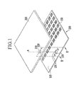
- FIG. 1 is a schematic oblique view illustrating a mask for deposition and a method for aligning a substrate according to an embodiment of the present invention.
- FIG. 2 is a schematic cross-sectional view taken along line II-II of FIG. 1 .
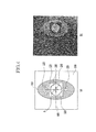
- FIGS. 3 through 5 are top plan views illustrating a case in which an alignment of a mask for deposition and a transparent substrate is measured by a measuring device according to an embodiment of the present invention.
- FIG. 6 is a schematic cross-sectional view illustrating a mask for deposition and a method for aligning a substrate according to an embodiment of the present invention.
- FIG. 7 is a graph illustrating a recognition rate of an alignment mark after the mark for deposition according to the embodiment of the present invention and a transparent substrate are aligned and the alignment mark is photographed.
- on means one located above or below a targeted portion and does not necessarily mean one located on the top based on a gravity direction.
- FIG. 1 is a schematic oblique view illustrating a mask for deposition and a method for aligning a substrate according to an embodiment of the present invention
- FIG. 2 is a schematic cross-sectional view taken along line II-II of FIG. 1
- a mask 100 for deposition is a mask for forming a pattern on a transparent substrate 200 and is configured to include a mask member 105 and an unevenness region 130.
- the transparent substrate 200 is a substrate for forming an organic light emitting diode (OLED) display device and may be further provided with a transparent barrier film 210.
- the transparent substrate 200 may be made of a flexible material.
- a first electrode layer serving as an anode is formed on the transparent barrier film 210
- an organic emission layer is formed on the first electrode layer
- a second electrode layer serving as a cathode is formed on the organic emission layer.
- the first electrode layer may be formed to have a predetermined pattern on the transparent substrate 200 by vacuum deposition or sputtering and the second electrode layer may be molded to have a predetermined pattern by the vacuum deposition, and the like, after the first electrode layer and the organic emission layer are formed.
- the organic emission layer may be formed by deposition, spin coating, inkjet printing, and the like.
- the organic emission layer may have a structure of a multilayered film at least including an emission layer.
- an electron transport layer may be disposed between the second electrode layer and the organic emission layer
- a hole transport layer may be disposed between the first electrode layer and the organic emission layer
- a hole injection layer HIL
- an electron injection layer EIL
- ETL electron transport layer Due to the foregoing multilayer structure, holes and electrons can be more smoothly transported into the organic emission layer.
- the mask 100 for deposition formed with an open region 150 so as to correspond to each pattern is used in a process of adopting a deposition method so as to form an electrode layer having a predetermined pattern and the organic emission layer.
- the mask for deposition adheres to the transparent substrate 200 by a vacuum adsorption means or a mask support means such as a magnet unit.
- line A indicates an alignment line for aligning the mask 100 for deposition and the transparent substrate 200.
- a substrate alignment mark 230 and an angle alignment mark 220 are formed on one surface of the transparent substrate 200 for alignment.
- the substrate alignment mark 230 which is a mark for confirming an alignment state with a mask, is a means for determining whether or not to be matched with the mask alignment mark 110 to be described below.
- the present embodiment describes that the substrate alignment mark 230 is formed in a cross (+) shape, but is not limited thereto and therefore, the substrate alignment mark 230 may be formed in various shapes of diagrams.
- the angle alignment mark 220 may be disposed while an angle of a substrate deviates from a predetermined reference even though the substrate alignment mark 230 is matched with the mask alignment mark 110. Therefore, the angle alignment mark 220 is adjacently formed to the substrate alignment mark 230 which is a means for preventing a warpage of a substrate.
- the present embodiment describes that the angle alignment mark 220 is formed in a quadrangular shape, but is not limited thereto, and therefore the angle alignment mark 220 may be formed in various shapes of diagrams.
- the substrate alignment mark 230 and the mask alignment mark 110 are adjacently formed to each other but are spaced apart from each other with a predetermined distance.
- the mask member 105 is a plate-shaped member including the open region 150 formed to correspond to a pattern of an object to be deposited and a material of the mask member 105 may be a metal material such as metal or alloy, a functional polymer, or a mixture of polymer and metal.
- the open region 150 may be provided with a plurality of slits that are formed by penetrating through the mask 100 for deposition.
- the open region 150 may have a pattern corresponding to the first electrode layer, the organic emission layer, and the second electrode layer.
- the mask alignment mark 110 which is a mark for aligning the transparent substrate 200 and the mask 100 for deposition, is formed as the open region by penetrating the mask member 105.
- the present embodiment of the present invention describes that the mask alignment mark 110 has a circular shape, but is not limited thereto, and therefore the mask alignment mark 100 may have various shapes of polygons, such as triangle, quadrangle, and the like.
- an area of the mask alignment mark 110 may be larger than that of the substrate alignment mark 230 so that the substrate alignment mark 230 may be disposed within a region of the mask alignment mark 110.
- at least two mask alignment marks 110 may be formed at an outside of the mask member 105.
- the unevenness region 130 is formed on one surface of the mask member 105 so as to be adjacent to the mask alignment mark 110 and the unevenness region 130 having protrusions and depressions is formed on a surface thereof. As shown in FIG. 2 , the unevenness region 130 has a bent surface on which a plurality of ridges and valleys are repeated. Due to the foregoing features, the unevenness region 130 may be diffused-reflect incident light. At the time of performing measurement by a measuring device 300 (in reference to FIG. 6 ), the unevenness region 130 appears darker than periphery by diffused-reflecting incident light from the measuring device.
- the angle alignment mark 220 When the angle alignment mark 220 is disposed in a region rather than in the unevenness region 130, it is difficult to recognize the angle alignment mark 220 due to light reflected from the surface of the mask 100 for deposition. In other words, in the present embodiment where the angle alignment mark 220 is disposed within the unevenness region 130 as shown in FIG. 2 , it is possible to prevent the angle alignment mark 220 of the transparent substrate 200 disposed on the unevenness region 130 from not being recognized by the measuring device 300 due to reflected light, by preventing the incident light from the measuring device 300 from being reflected from the unevenness region 130.
- FIGS. 3 through 5 are top plan views illustrating the case in which the alignment of the mask for deposition and the transparent substrate is measured by the measuring device according to an embodiment.
- FIGS. 3(b) and 4(b) illustrate photographs in which the mask for deposition according to the embodiment of the present invention is taken by a charge-coupled device (CCD) camera.
- CCD charge-coupled device
- an unevenness region 131 may be formed around the mask alignment mark 110 by being divided into at least two while being spaced apart from the mask alignment mark 110; as illustrated in FIGS. 4(a) and 5 , an unevenness region 132, 133 may be formed as a continuous element to surround the periphery of the mask alignment mark 110 while being spaced apart from the mask alignment mark 110.
- the present embodiments of the present invention describe that the entire shape of the unevenness region 130 has an oval shape, but are not limited thereto. Therefore, the unevenness region 130 may have various shapes.
- the area of the unevenness region 130 may be formed to be larger than that of the angle alignment mark 220 so that the angle alignment mark 220 disposed within the unevenness region 130 may be easily differentiated.
- the unevenness region 130 may be formed to have a height lower than one surface of the mask 100 for deposition by partially cutting the surface of the mask 100 for deposition.
- the unevenness region 130 may be formed by one selected from various processes, such as half etching, laser, a photolithography process, a sand blast process, and the like.
- the unevenness region 130 is not damaged even though the mask 100 for deposition adheres to the transparent substrate 200.
- the unevenness region 130 may be coated with a diffused reflection material that may diffused-reflect light according to the reaction of a wavelength of light with a molecular particle of a material. In this case, it is possible to more effectively diffused-reflect the incident light.
- a flat region 120 (121, 122, 123 as shown respectively in FIG, 3(a) and FIG. 4(a) and FIG. 5 ) with a flat surface may be further disposed between the mask alignment mark 110 and the unevenness region 130.
- the flat region 120 may reflect the incident light.
- the mask alignment mark 110 is opened to transmit light that is incident in a substrate direction, while the flat region 120 reflects light that is incident in the substrate direction, such that the mask alignment mark 110 is displayed at low brightness and the flat region 120 is displayed at high brightness at the time of performing the measurement by the measuring device 300.
- the difference in contrast between the mask alignment mark 110 and the flat region 120 is distinct so that the mask alignment mark 110 can be easily differentiated.
- the flat region 120 has a difference in contrast from the unevenness region 130 according to the foregoing principle, such that the mask alignment mark 110 and the unevenness region 130 can be easily differentiated.
- the flat region 120 may be formed along a boundary of the mask alignment mark 110 so as to easily differentiate the mask alignment mark 110 and may be formed by being coated with a light reflection material reflecting light that is incident according to the reaction of a wavelength of light with a molecular particle of a material.
- the flat region 121 is formed to surround the boundary of the mask alignment mark 110 to geometrically isolate the unevenness region 131 and the mask alignment mark 110; as illustrated in FIGS. 4(a) and 5 , the flat regions 122 and 123 are formed to surround the boundary of the mask alignment mark 110 but may be formed in some region of the inside of the unevenness regions 132 and 133.
- the present embodiment of the present invention describes that the entire shape of the flat region 120 surrounding the mask alignment mark 110 has a quadrangle 122 (see FIG. 4 ) and a circle 123 (see FIG. 5 ), but is not limited thereto and may be variously changed among shapes that can space between the mask alignment mark 110 and the unevenness regions 132, 133 while surrounding the mask alignment mark 110.
- FIG. 6 is a schematic view illustrating a mask for deposition and a method for aligning a substrate according to an embodiment of the present invention.
- the transparent substrate 200 having one surface S1 on which the substrate alignment mark 230 and the angle alignment mark 220 adjacently formed to the substrate alignment mark 230 are formed is prepared and then, the transparent substrate 200 is seated on a substrate support member (not shown).
- a substrate support member not shown.
- the mask 100 for deposition according to the embodiment of the present invention is disposed on the transparent substrate 200 and the transparent substrate 200 is adhered to the mask 100 for deposition by the mask support means.
- the mask 100 for deposition on which the unevenness region 130 is formed is disposed so that one surface S2 thereof faces the transparent substrate 200.
- the substrate alignment mark 230 and the mask alignment mark 110 are aligned so as to be disposed at a predetermined location.
- the locations of the substrate alignment mark 230 and the mask alignment mark 110 are confirmed by measuring the alignment state by the measuring device 300 that is disposed so as to face the unevenness region 130.
- the predetermined location refers to a location that is input to the measuring device 300 mounted with a CCD camera in advance and may correspond to, for example, reference lines 310, 315, and 320 illustrated in FIGS. 3 through 5 .
- a central portion of the substrate alignment mark 230 having a cross shape is disposed at a central portion at which a vertical reference line 310 intersects a horizontal reference line 315, and a circular central line 320 may be formed to have the same size as the circular mask alignment mark 110 so as to match the mask alignment mark 110 (for convenience, shown in the drawings so as not to match each other).
- the shapes of the reference lines 310, 315, and 320 are by way of example and therefore, the reference lines 310, 315, and 320 may be formed to have various shapes according to colors, shapes, and the like, of the alignment mark.
- the brightness is reduced by transmitting the incident light from the CCD camera through the mask alignment mark 110 of the mask 100 for deposition that is an opened region, while the brightness is increased due to the reflection of the incident light from the flat region 120.
- the mask alignment mark 110 may be easily identified due to the distinct difference in contrast between the mask alignment mark 110 and the flat region 120, such that it may be detected whether the mask 100 for deposition is disposed at a desired location.
- the substrate alignment mark 230 located at a center of the mask alignment mark 110 reflects the incident light to increase the brightness, such that it is possible to easily differentiate the mask alignment mark 110.
- the substrate support member moves or the transparent substrate 200 or the mask 100 for deposition moves through a mask driving member (not shown) so as to be disposed at a predetermined location.
- the angle alignment mark 220 is aligned so as to be disposed at a predetermined location while the angle alignment mark 220 overlaps the unevenness region 130.
- the predetermined location refers to a location that is input to the measuring device 300 mounted with the CCD camera and may correspond to, for example, the vertical reference line 310 illustrated in FIGS. 3 through 5 .
- Both of the substrate alignment mark 230 and the angle alignment mark 220 are aligned so as to match the vertical reference line 310 so that it is possible to prevent the transparent substrate 200 from being disposed while being deviated from the mask 100 for deposition.
- the substrate support member moves or the transparent substrate 200 or the mask 100 for deposition moves through the mask driving member so as to be disposed at the predetermined location.
- the incident light from the CCD camera is diffused-reflected in the unevenness region 130 to reduce the brightness and is reflected in the flat region adjacent to the unevenness region 130 to increase the brightness, such that the difference in brightness between the unevenness region 130 and the flat region 120 is distinct.
- the angle alignment mark 220 can be easily recognized.
- FIG. 7 is a graph illustrating a recognition rate of an align mark after the mark for deposition according to the embodiment of the present invention and a transparent substrate are aligned and the align mark is photographed.
- a recognition rate shows how much the shape of the stored image and the shape actually measured by the measuring device overlap each other after an image for the shapes of the alignment marks 220 and 230 formed on the transparent substrate 200 and the mask alignment mark 110 is stored in the measuring device 300, that is, a ratio of an overlapping area with the entire area of the shape. That is, when the shape of the stored image and the actually measured shape completely overlap, the recognition rate corresponds to 100% and when the shape of the stored image and the actually measured shape completely do not overlap, the recognition rate corresponds to 0%. It is preferable that the recognition rate is experimentally 95% or more.
- Experimental Example 1 of FIG. 7 is an alignment mark recognition rate after being aligned using the mask for deposition formed as shown in FIG. 3 and Experimental Example 2 is an alignment mark recognition rate after being aligned using the mask for deposition formed as shown in FIG. 4 .
- the deposition mask of Comparative Example 1 is formed to have the same shape as Experimental Example 1, but does not have the unevenness region.
- the deposition mask of Comparative Example 2 is formed to have the same shape as Experimental Example 2, but does not have the unevenness region.
- each of the masks for deposition of Experimental Examples and Comparative Examples includes two mask alignment marks 110 and includes the substrate alignment mark 230, the angle alignment mark 220, the unevenness region 130, the flat region 120, and the like, to correspond to the mask alignment mark 110.
- the two alignment marks 110 are measured by the two measuring device 300, which are each shown by C1 and C2 in FIG. 7 .
- Comparative Example 1 and Comparative Example 2 show a distribution of the recognition rate of 88 to 96 % according to the experimental frequency, while both of the Experimental Example 1 and Experimental Example 2 show the recognition rate of 96 % or more. It may be appreciated that the alignment mark recognition rates of the masks for deposition formed according to the embodiments of the present invention are higher by diffused-reflecting the incident light in the unevenness region.
Landscapes
- Chemical & Material Sciences (AREA)
- Engineering & Computer Science (AREA)
- Chemical Kinetics & Catalysis (AREA)
- Materials Engineering (AREA)
- Mechanical Engineering (AREA)
- Metallurgy (AREA)
- Organic Chemistry (AREA)
- Manufacturing & Machinery (AREA)
- Electroluminescent Light Sources (AREA)
- Physical Vapour Deposition (AREA)
Abstract
Description
- An embodiment of the present invention relates generally to a mask for deposition and a method for aligning the same, and more particularly, to a mask for deposition and a method for aligning the same capable of precisely aligning a mask for deposition and a substrate.
- An organic light emitting diode (OLED) display device, which includes a hole injection electrode, an electron injection electrode, and an organic emission layer disposed therebetween, is a self-emitting type display device emitting light while annihilating holes injected from an anode and electrons injected from a cathode due to the recombination of the holes and electrons in the organic emission layer. In addition, the organic light emitting diode (OLED) display device exhibits high-quality characteristics such as lower power consumption, higher luminance, a wider viewing angle, and a higher reaction speed and therefore, has been focused as a next generation display device of a portable electronic device.
- The organic light emitting diode (OLED) display device includes an organic light emitting display panel including a display substrate on which a thin film transistor and an organic light emitting element (OLED) are formed. The organic light emitting element includes an anode, a cathode, and an organic emission layer and emits light by forming excitons by holes and electrons injected from each of the anode and the cathode and shifting the excitons to a ground state.
- In a flat panel display device such as the organic light emitting diode (OLED) display device, a vacuum deposition method for depositing corresponding materials such as an organic material or metals used as an electrode under the vacuum atmosphere to form a thin film on a flat panel, has been used. The vacuum deposition method is performed by disposing a substrate on which an organic thin film is grown in an interior of a vacuum chamber and by evaporating or sublimating the organic materials using a deposition source unit so as to be deposited on the substrate.
- The deposition process is performed by aligning and attaching a mask for deposition including an open region, which is formed to correspond to a predetermined pattern to be formed on the substrate, on the substrate and performing a control so as to deposit a material for forming an evaporated pattern on the substrate through the open region. In the deposition process, it is important to correctly align and attach the mask for deposition on the substrate without errors.
- When the substrate is a transparent substrate, however, a contrast difference between alignment marks, in particular, an angle alignment mark and a substrate (and a mask) is small due to the reflected light from the mask surface at the time of performing the measurement by the measuring device and therefore, it is difficult to confirm a location of the angle alignment mark.
- The above information disclosed in this Background section is only for enhancement of understanding of the background of the described technology and therefore it may contain information that does not form the prior art that is already known in this country to a person of ordinary skill in the art.
- An aspect of the present invention provides a mask for deposition and a method for aligning the same capable of preventing an alignment error between a substrate and a mask from occurring.
- Another aspect of the present invention provides a mask for deposition and a method for aligning the same capable of increasing a recognition rate of alignment marks formed on a substrate and a mask.
- An embodiment of the present invention provides a mask for deposition for forming a pattern on a transparent substrate including: a mask member having a mask alignment mark penetratedly formed so as to be aligned with a substrate alignment mark formed on the transparent substrate; and an unevenness region formed on one surface of the mask member so as to be adjacent to the mask alignment mark and having protrusions and depressions on a surface thereof.
- The unevenness region may diffused-reflect incident light.
- The unevenness region may be coated with a diffused-reflection material.
- The unevenness region may be formed at a height lower than one surface of the mask for deposition.
- The unevenness region may be formed by half etching.
- The mask for deposition may further include a flat region formed between the mask alignment mark and the unevenness region and having a flat surface.
- The flat region may be formed along a periphery of the mask alignment mark.
- The flat region may reflect incident light.
- The flat region may be coated with a light reflection material.
- The unevenness region may be formed to surround an entirety of the mask alignment mark.
- The unevenness region may comprise two parts being spaced apart from the mask alignment mark.
- Another embodiment of the present invention provides a method for aligning a mask, including steps of: preparing a transparent substrate having a substrate alignment mark and an angle alignment mark formed adjacent to the substrate alignment mark formed on one surface of the transparent substrate; disposing a mask for deposition on the transparent substrate, the mask including a mask member having a mask alignment mark penetratedly formed so as to be aligned with a substrate alignment mark formed on the transparent substrate and an unevenness region formed on one surface of the mask member so as to be adjacent to the mask alignment mark, the unevenness region having protrusions and depressions on a surface thereof, the unevenness region facing the transparent substrate; aligning the substrate alignment mark and the mask alignment mark at a predetermined location; and aligning the angle alignment mark so that the angle alignment mark is disposed at a predetermined location while overlapping the unevenness region.
- In the steps of aligning of the location or the aligning of the angle, after an alignment state is measured by a measuring device that is disposed so as to face the unevenness region, an alignment location of the transparent substrate or the mask for deposition may be adjusted.
- The measuring device may be a measuring device mounted with a CCD camera.
- Yet another embodiment of the present invention provides a mask for deposition for forming a pattern on a transparent substrate, comprising a mask member having a mask alignment mark penetrating the mask member; and an unevenness region disposed on at least two opposite sides of the mask alignment mark, the unevenness region comprising a non-flat surface which diffused-reflects light incident on the non-flat surface of the unevenness region.
- According to the embodiments of the present invention, it is possible to prevent the alignment error of the mask from occurring by increasing the recognition rate of the alignment marks formed on the substrate and the mask.
- As a result, it is possible to reduce the manufacturing costs by reducing the defective rate of the organic light emitting diode (OLED) display device.
- A more complete appreciation of the invention, and many of the attendant advantages thereof, will be readily apparent as the same becomes better understood by reference to the following detailed description when considered in conjunction with the accompanying drawings in which like reference symbols indicate the same or similar components, wherein:
-
FIG. 1 is a schematic oblique view illustrating a mask for deposition and a method for aligning a substrate according to an embodiment of the present invention. -
FIG. 2 is a schematic cross-sectional view taken along line II-II ofFIG. 1 . -
FIGS. 3 through 5 are top plan views illustrating a case in which an alignment of a mask for deposition and a transparent substrate is measured by a measuring device according to an embodiment of the present invention. -
FIG. 6 is a schematic cross-sectional view illustrating a mask for deposition and a method for aligning a substrate according to an embodiment of the present invention. -
FIG. 7 is a graph illustrating a recognition rate of an alignment mark after the mark for deposition according to the embodiment of the present invention and a transparent substrate are aligned and the alignment mark is photographed. - Hereinafter, a mask for deposition and a method for aligning the same according to the present invention will be described in detail with reference to the accompanying drawings. However, the present invention is not limited to the exemplary embodiments disclosed below but may be implemented in various types. Therefore, the present exemplary embodiments are provided to fully describe the present invention and fully inform those skilled in the art of the scope of the present invention. Like reference numerals designate like elements throughout the specification.
- In the drawings, the thickness of layers, films, panels, regions, etc., are exaggerated for clarity. Further, the thicknesses of some layers and regions are exaggerated in the drawings for better understanding and ease of description. It will be understood that when an element such as a layer, film, region, or substrate is referred to as being "on" another element, it can be directly on the other element or intervening elements may also be present.
- In addition, unless explicitly described to the contrary, the word "comprise" and variations such as "comprises" or "comprising", will be understood to imply the inclusion of stated elements but not the exclusion of any other elements.
- In addition, throughout the specification, "on" means one located above or below a targeted portion and does not necessarily mean one located on the top based on a gravity direction.
-
FIG. 1 is a schematic oblique view illustrating a mask for deposition and a method for aligning a substrate according to an embodiment of the present invention andFIG. 2 is a schematic cross-sectional view taken along line II-II ofFIG. 1 - In reference to
FIGS. 1 and2 , amask 100 for deposition according to an embodiment of the present invention is a mask for forming a pattern on atransparent substrate 200 and is configured to include amask member 105 and anunevenness region 130. - The
transparent substrate 200 is a substrate for forming an organic light emitting diode (OLED) display device and may be further provided with atransparent barrier film 210. Thetransparent substrate 200 may be made of a flexible material. Although not illustrated inFIG. 1 , a first electrode layer serving as an anode is formed on thetransparent barrier film 210, an organic emission layer is formed on the first electrode layer, and a second electrode layer serving as a cathode is formed on the organic emission layer. - The first electrode layer may be formed to have a predetermined pattern on the
transparent substrate 200 by vacuum deposition or sputtering and the second electrode layer may be molded to have a predetermined pattern by the vacuum deposition, and the like, after the first electrode layer and the organic emission layer are formed. Further, the organic emission layer may be formed by deposition, spin coating, inkjet printing, and the like. The organic emission layer may have a structure of a multilayered film at least including an emission layer. For example, an electron transport layer (ETL) may be disposed between the second electrode layer and the organic emission layer, a hole transport layer (HTL) may be disposed between the first electrode layer and the organic emission layer, a hole injection layer (HIL) may be disposed between the first electrode layer and the hole transport layer, an electron injection layer (EIL) may be disposed between the second electrode layer and the electron transport layer (ETL). Due to the foregoing multilayer structure, holes and electrons can be more smoothly transported into the organic emission layer. - In the manufacture of the organic light emitting diode (OLED) display device having the foregoing configuration, the
mask 100 for deposition formed with anopen region 150 so as to correspond to each pattern is used in a process of adopting a deposition method so as to form an electrode layer having a predetermined pattern and the organic emission layer. The mask for deposition adheres to thetransparent substrate 200 by a vacuum adsorption means or a mask support means such as a magnet unit. - The
mask 100 for deposition and thetransparent substrate 200 are accurately disposed at a predetermined location so as to accurately form the pattern at a desired location. InFIG. 1 , line A indicates an alignment line for aligning themask 100 for deposition and thetransparent substrate 200. Asubstrate alignment mark 230 and anangle alignment mark 220 are formed on one surface of thetransparent substrate 200 for alignment. Thesubstrate alignment mark 230, which is a mark for confirming an alignment state with a mask, is a means for determining whether or not to be matched with themask alignment mark 110 to be described below. The present embodiment describes that thesubstrate alignment mark 230 is formed in a cross (+) shape, but is not limited thereto and therefore, thesubstrate alignment mark 230 may be formed in various shapes of diagrams. Theangle alignment mark 220 may be disposed while an angle of a substrate deviates from a predetermined reference even though thesubstrate alignment mark 230 is matched with themask alignment mark 110. Therefore, theangle alignment mark 220 is adjacently formed to thesubstrate alignment mark 230 which is a means for preventing a warpage of a substrate. The present embodiment describes that theangle alignment mark 220 is formed in a quadrangular shape, but is not limited thereto, and therefore theangle alignment mark 220 may be formed in various shapes of diagrams. Thesubstrate alignment mark 230 and themask alignment mark 110 are adjacently formed to each other but are spaced apart from each other with a predetermined distance. - The
mask member 105 is a plate-shaped member including theopen region 150 formed to correspond to a pattern of an object to be deposited and a material of themask member 105 may be a metal material such as metal or alloy, a functional polymer, or a mixture of polymer and metal. Theopen region 150 may be provided with a plurality of slits that are formed by penetrating through themask 100 for deposition. Theopen region 150 may have a pattern corresponding to the first electrode layer, the organic emission layer, and the second electrode layer. - The
mask alignment mark 110, which is a mark for aligning thetransparent substrate 200 and themask 100 for deposition, is formed as the open region by penetrating themask member 105. The present embodiment of the present invention describes that themask alignment mark 110 has a circular shape, but is not limited thereto, and therefore themask alignment mark 100 may have various shapes of polygons, such as triangle, quadrangle, and the like. When themask alignment mark 110 and thesubstrate alignment mark 230 are aligned, an area of themask alignment mark 110 may be larger than that of thesubstrate alignment mark 230 so that thesubstrate alignment mark 230 may be disposed within a region of themask alignment mark 110. Further, for the precise alignment with thetransparent substrate 200, at least two mask alignment marks 110 may be formed at an outside of themask member 105. - The
unevenness region 130 is formed on one surface of themask member 105 so as to be adjacent to themask alignment mark 110 and theunevenness region 130 having protrusions and depressions is formed on a surface thereof. As shown inFIG. 2 , theunevenness region 130 has a bent surface on which a plurality of ridges and valleys are repeated. Due to the foregoing features, theunevenness region 130 may be diffused-reflect incident light. At the time of performing measurement by a measuring device 300 (in reference toFIG. 6 ), theunevenness region 130 appears darker than periphery by diffused-reflecting incident light from the measuring device. When theangle alignment mark 220 is disposed in a region rather than in theunevenness region 130, it is difficult to recognize theangle alignment mark 220 due to light reflected from the surface of themask 100 for deposition. In other words, in the present embodiment where theangle alignment mark 220 is disposed within theunevenness region 130 as shown inFIG. 2 , it is possible to prevent theangle alignment mark 220 of thetransparent substrate 200 disposed on theunevenness region 130 from not being recognized by the measuringdevice 300 due to reflected light, by preventing the incident light from the measuringdevice 300 from being reflected from theunevenness region 130. -
FIGS. 3 through 5 are top plan views illustrating the case in which the alignment of the mask for deposition and the transparent substrate is measured by the measuring device according to an embodiment.FIGS. 3(b) and 4(b) illustrate photographs in which the mask for deposition according to the embodiment of the present invention is taken by a charge-coupled device (CCD) camera. - As illustrated in
FIG. 3(a) , anunevenness region 131 may be formed around themask alignment mark 110 by being divided into at least two while being spaced apart from themask alignment mark 110; as illustrated inFIGS. 4(a) and5 , anunevenness region mask alignment mark 110 while being spaced apart from themask alignment mark 110. - The present embodiments of the present invention describe that the entire shape of the
unevenness region 130 has an oval shape, but are not limited thereto. Therefore, theunevenness region 130 may have various shapes. The area of theunevenness region 130 may be formed to be larger than that of theangle alignment mark 220 so that theangle alignment mark 220 disposed within theunevenness region 130 may be easily differentiated. - As shown in
FIG. 2 , theunevenness region 130 may be formed to have a height lower than one surface of themask 100 for deposition by partially cutting the surface of themask 100 for deposition. In this case, theunevenness region 130 may be formed by one selected from various processes, such as half etching, laser, a photolithography process, a sand blast process, and the like. When theunevenness region 130 is formed at a height lower than one surface of themask 100 for deposition, theunevenness region 130 is not damaged even though themask 100 for deposition adheres to thetransparent substrate 200. - The
unevenness region 130 may be coated with a diffused reflection material that may diffused-reflect light according to the reaction of a wavelength of light with a molecular particle of a material. In this case, it is possible to more effectively diffused-reflect the incident light. - A flat region 120 (121, 122, 123 as shown respectively in
FIG, 3(a) and FIG. 4(a) andFIG. 5 ) with a flat surface may be further disposed between themask alignment mark 110 and theunevenness region 130. Theflat region 120 may reflect the incident light. Themask alignment mark 110 is opened to transmit light that is incident in a substrate direction, while theflat region 120 reflects light that is incident in the substrate direction, such that themask alignment mark 110 is displayed at low brightness and theflat region 120 is displayed at high brightness at the time of performing the measurement by the measuringdevice 300. As such, the difference in contrast between themask alignment mark 110 and theflat region 120 is distinct so that themask alignment mark 110 can be easily differentiated. Theflat region 120 has a difference in contrast from theunevenness region 130 according to the foregoing principle, such that themask alignment mark 110 and theunevenness region 130 can be easily differentiated. - The
flat region 120 may be formed along a boundary of themask alignment mark 110 so as to easily differentiate themask alignment mark 110 and may be formed by being coated with a light reflection material reflecting light that is incident according to the reaction of a wavelength of light with a molecular particle of a material. - As shown in
FIG. 3(a), when theunevenness region 131 is formed around themask alignment mark 110 by being divided into at least two, theflat region 121 is formed to surround the boundary of themask alignment mark 110 to geometrically isolate theunevenness region 131 and themask alignment mark 110; as illustrated inFIGS. 4(a) and5 , theflat regions mask alignment mark 110 but may be formed in some region of the inside of theunevenness regions - The present embodiment of the present invention describes that the entire shape of the
flat region 120 surrounding themask alignment mark 110 has a quadrangle 122 (seeFIG. 4 ) and a circle 123 (seeFIG. 5 ), but is not limited thereto and may be variously changed among shapes that can space between themask alignment mark 110 and theunevenness regions mask alignment mark 110. - Hereinafter, the use of the mask for deposition and the method for aligning the same according to the exemplary embodiment will be described with reference to the accompanying drawings.
-
FIG. 6 is a schematic view illustrating a mask for deposition and a method for aligning a substrate according to an embodiment of the present invention. - Referring to
FIGS. 1 and6 , thetransparent substrate 200 having one surface S1 on which thesubstrate alignment mark 230 and theangle alignment mark 220 adjacently formed to thesubstrate alignment mark 230 are formed is prepared and then, thetransparent substrate 200 is seated on a substrate support member (not shown). The features of thesubstrate alignment mark 230 and theangle alignment mark 220 adjacently formed thereto are already described. - The
mask 100 for deposition according to the embodiment of the present invention is disposed on thetransparent substrate 200 and thetransparent substrate 200 is adhered to themask 100 for deposition by the mask support means. In this case, themask 100 for deposition on which theunevenness region 130 is formed is disposed so that one surface S2 thereof faces thetransparent substrate 200. - Next, the
substrate alignment mark 230 and themask alignment mark 110 are aligned so as to be disposed at a predetermined location. In this case, the locations of thesubstrate alignment mark 230 and themask alignment mark 110 are confirmed by measuring the alignment state by the measuringdevice 300 that is disposed so as to face theunevenness region 130. The predetermined location refers to a location that is input to themeasuring device 300 mounted with a CCD camera in advance and may correspond to, for example,reference lines FIGS. 3 through 5 . A central portion of thesubstrate alignment mark 230 having a cross shape is disposed at a central portion at which avertical reference line 310 intersects ahorizontal reference line 315, and a circularcentral line 320 may be formed to have the same size as the circularmask alignment mark 110 so as to match the mask alignment mark 110 (for convenience, shown in the drawings so as not to match each other). The shapes of thereference lines reference lines - When being photographed by the CCD camera that is mounted in the
measuring device 300, the brightness is reduced by transmitting the incident light from the CCD camera through themask alignment mark 110 of themask 100 for deposition that is an opened region, while the brightness is increased due to the reflection of the incident light from theflat region 120. Themask alignment mark 110 may be easily identified due to the distinct difference in contrast between themask alignment mark 110 and theflat region 120, such that it may be detected whether themask 100 for deposition is disposed at a desired location. In addition, thesubstrate alignment mark 230 located at a center of themask alignment mark 110 reflects the incident light to increase the brightness, such that it is possible to easily differentiate themask alignment mark 110. When thesubstrate alignment mark 230 or themask alignment mark 110 are not disposed at a predetermined location, the substrate support member moves or thetransparent substrate 200 or themask 100 for deposition moves through a mask driving member (not shown) so as to be disposed at a predetermined location. - Next, the
angle alignment mark 220 is aligned so as to be disposed at a predetermined location while theangle alignment mark 220 overlaps theunevenness region 130. In this case, the locations of theangle alignment mark 220 and theunevenness region 130 are confirmed by measuring the alignment state by the measuringdevice 300 that is disposed so as to face theunevenness region 130. The predetermined location refers to a location that is input to themeasuring device 300 mounted with the CCD camera and may correspond to, for example, thevertical reference line 310 illustrated inFIGS. 3 through 5 . Both of thesubstrate alignment mark 230 and theangle alignment mark 220 are aligned so as to match thevertical reference line 310 so that it is possible to prevent thetransparent substrate 200 from being disposed while being deviated from themask 100 for deposition. When theangle alignment mark 220 is not disposed at the predetermined location, the substrate support member moves or thetransparent substrate 200 or themask 100 for deposition moves through the mask driving member so as to be disposed at the predetermined location. - When being photographed by the CCD camera mounted with the measuring device, the incident light from the CCD camera is diffused-reflected in the
unevenness region 130 to reduce the brightness and is reflected in the flat region adjacent to theunevenness region 130 to increase the brightness, such that the difference in brightness between theunevenness region 130 and theflat region 120 is distinct. When the brightness is reduced in theunevenness region 130 so as to dispose theangle alignment mark 220 in theunevenness region 130, theangle alignment mark 220 can be easily recognized. - By the foregoing method, a process of aligning the
transparent substrate 200 and themask 100 for deposition and then, deposition of the organic material is performed. - Hereinafter, the use of the mask for deposition and an effect of the method for aligning the same according to the exemplary embodiment will be described with reference to the accompanying drawings.
-
FIG. 7 is a graph illustrating a recognition rate of an align mark after the mark for deposition according to the embodiment of the present invention and a transparent substrate are aligned and the align mark is photographed. - A recognition rate shows how much the shape of the stored image and the shape actually measured by the measuring device overlap each other after an image for the shapes of the alignment marks 220 and 230 formed on the
transparent substrate 200 and themask alignment mark 110 is stored in themeasuring device 300, that is, a ratio of an overlapping area with the entire area of the shape. That is, when the shape of the stored image and the actually measured shape completely overlap, the recognition rate corresponds to 100% and when the shape of the stored image and the actually measured shape completely do not overlap, the recognition rate corresponds to 0%. It is preferable that the recognition rate is experimentally 95% or more. - Experimental Example 1 of
FIG. 7 is an alignment mark recognition rate after being aligned using the mask for deposition formed as shown inFIG. 3 and Experimental Example 2 is an alignment mark recognition rate after being aligned using the mask for deposition formed as shown inFIG. 4 . The deposition mask of Comparative Example 1 is formed to have the same shape as Experimental Example 1, but does not have the unevenness region. The deposition mask of Comparative Example 2 is formed to have the same shape as Experimental Example 2, but does not have the unevenness region. Further, each of the masks for deposition of Experimental Examples and Comparative Examples includes two mask alignment marks 110 and includes thesubstrate alignment mark 230, theangle alignment mark 220, theunevenness region 130, theflat region 120, and the like, to correspond to themask alignment mark 110. The twoalignment marks 110 are measured by the twomeasuring device 300, which are each shown by C1 and C2 inFIG. 7 . - It may be appreciated that Comparative Example 1 and Comparative Example 2 show a distribution of the recognition rate of 88 to 96 % according to the experimental frequency, while both of the Experimental Example 1 and Experimental Example 2 show the recognition rate of 96 % or more. It may be appreciated that the alignment mark recognition rates of the masks for deposition formed according to the embodiments of the present invention are higher by diffused-reflecting the incident light in the unevenness region.
- While this disclosure has been described in connection with what is presently considered to be practical exemplary embodiments, it is to be understood that the invention is not limited to the disclosed embodiments, but, on the contrary, is intended to cover various modifications and equivalent arrangements included within the scope of the appended claims.
Claims (14)
- A mask for deposition for forming a pattern on a transparent substrate (200), comprising:a mask member (105) having a mask alignment mark (110) penetratedly formed so as to be aligned with a substrate alignment mark (230) formed on the transparent substrate (200); andan unevenness region (130; 131; 132; 133) formed on one surface of the mask member (105) so as to be adjacent to the mask alignment mark (110), a surface of the unevenness region (130; 131; 132; 133) comprising protrusions and depressions.
- The mask for deposition of claim 1, wherein the unevenness region (130; 131; 132; 133) diffused-reffects light incident on the surface of the unevenness region (130; 131; 132; 133).
- The mask for deposition of claim 1 or 2, wherein the unevenness region (130; 131; 132; 133) is coated with a diffused-reflection material.
- The mask for deposition of one of the preceeding claims, wherein the unevenness region (130; 131; 132; 133) is formed at a height lower than one surface of the mask (100) for deposition.
- The mask for deposition of one of the preceeding claims, wherein the unevenness region (130; 131; 132; 133) is formed by half etching.
- The mask for deposition of one of the preceeding claims, further comprising a flat region (120) formed between the mask alignment mark (110) and the unevenness region (130; 131; 132; 133), the flat region (120) having a flat surface.
- The mask for deposition of claim 6, wherein the flat region (120) is formed along a periphery of the mask alignment mark (110).
- The mask for deposition of claim 6 or 7, wherein the flat region (120) reflects light incident on the flat surface of the flat region (120).
- The mask for deposition of one of claims 6 to 8, wherein the flat region (120) is coated with a light reflection material.
- The mask for deposition of one of claims 6 to 9, wherein the unevenness region (132; 133) being formed to surround an entirety of the mask alignment mark (110).
- The mask for deposition of one of claims 6 to 9, wherein the unevenness region (131) comprises two parts being spaced apart from the mask alignment mark (110).
- A method for aligning a mask (100), comprising:preparing a transparent substrate (200) having a substrate alignment mark (230) and an angle alignment mark (220) formed adjacent to the substrate alignment mark (230) formed on one surface of the transparent substrate (200);disposing a mask (100) for deposition on the transparent substrate (200), with the mask (100) comprising a mask member (105) having a mask alignment mark (110) penetratedly formed so as to be aligned with the substrate alignment mark (230) formed on the transparent substrate (200) and an unevenness region (130; 131; 132; 133) formed on one surface of the mask member (105) so as to be adjacent to the mask alignment mark (110), a surface of the unevenness region (130; 131; 132; 133) having protrusions and depressions, the unevenness region (130; 131; 132; 133) facing the transparent substrate (200);aligning the substrate alignment mark (230) and the mask alignment mark (110) at a predetermined location; andaligning the angle alignment mark (220) so that the angle alignment mark (220) is disposed at a predetermined location while overlapping the unevenness region (130; 131; 132; 133).
- The method of claim 12, wherein:in the steps of aligning of the location or the aligning of the angle,after an alignment state is measured by a measuring device that is disposed so as to face the unevenness region (130; 131; 132; 133), an alignment location of the transparent substrate (200) or the mask (100) for deposition is adjusted.
- The method of claim 12 or 13, wherein:the measuring device is a measuring device (300) mounted with a CCD camera.
Applications Claiming Priority (1)
| Application Number | Priority Date | Filing Date | Title |
|---|---|---|---|
| KR1020120084200A KR20140017767A (en) | 2012-07-31 | 2012-07-31 | Mask for deposition and method for aligning the same |
Publications (1)
| Publication Number | Publication Date |
|---|---|
| EP2692896A1 true EP2692896A1 (en) | 2014-02-05 |
Family
ID=48877113
Family Applications (1)
| Application Number | Title | Priority Date | Filing Date |
|---|---|---|---|
| EP20130178356 Withdrawn EP2692896A1 (en) | 2012-07-31 | 2013-07-29 | Mask for deposition and method for aligning the same |
Country Status (6)
| Country | Link |
|---|---|
| US (1) | US9757764B2 (en) |
| EP (1) | EP2692896A1 (en) |
| JP (2) | JP2014031582A (en) |
| KR (1) | KR20140017767A (en) |
| CN (2) | CN203440443U (en) |
| TW (1) | TWI611030B (en) |
Cited By (3)
| Publication number | Priority date | Publication date | Assignee | Title |
|---|---|---|---|---|
| US10168148B2 (en) | 2016-01-29 | 2019-01-01 | Boe Technology Group Co., Ltd. | Display substrate, display device and method for recognizing position mark |
| EP3489384A4 (en) * | 2016-09-23 | 2019-09-04 | Kunshan Go-Visionox Opto-Electronics Co., Ltd. | FINE METAL MASK, DISPLAY SUBSTRATE, AND ALIGNMENT METHOD THEREOF |
| US10580371B2 (en) | 2015-10-09 | 2020-03-03 | Boe Technology Group Co., Ltd. | Data driving module for driving display panel, data driving method and display device |
Families Citing this family (29)
| Publication number | Priority date | Publication date | Assignee | Title |
|---|---|---|---|---|
| KR20140017767A (en) * | 2012-07-31 | 2014-02-12 | 삼성디스플레이 주식회사 | Mask for deposition and method for aligning the same |
| CN103839864A (en) * | 2014-02-24 | 2014-06-04 | 合肥鑫晟光电科技有限公司 | Coating alignment device and coating system |
| KR101436014B1 (en) * | 2014-04-29 | 2014-11-04 | 주식회사 미래솔루텍 | Evaporration mask |
| CN103966546B (en) * | 2014-04-29 | 2016-03-16 | 京东方科技集团股份有限公司 | A kind of metal mask plate |
| CN105624609B (en) * | 2014-11-21 | 2019-07-05 | 三星显示有限公司 | Deposition mas, the method for manufacturing deposition mas and the method for manufacturing display device |
| CN105988303B (en) * | 2015-02-26 | 2018-03-30 | 上海微电子装备(集团)股份有限公司 | A kind of mask transmitting device and transmission method |
| CN104900630B (en) * | 2015-06-07 | 2018-01-26 | 上海华虹宏力半导体制造有限公司 | Improve structure of alignment mark contrast and forming method thereof |
| KR102323357B1 (en) | 2015-07-21 | 2021-11-09 | 삼성디스플레이 주식회사 | Display apparatus |
| CN105097674B (en) * | 2015-09-07 | 2018-01-12 | 深圳市华星光电技术有限公司 | A kind of method for remaking scan line on the glass substrate |
| KR20170038964A (en) | 2015-09-30 | 2017-04-10 | 삼성디스플레이 주식회사 | Display Panel and method of manufacturing the same |
| CN105549320A (en) * | 2016-01-05 | 2016-05-04 | 京东方科技集团股份有限公司 | Alignment marking structure, mask plate, substrate and alignment method |
| KR102544244B1 (en) * | 2016-07-19 | 2023-06-19 | 삼성디스플레이 주식회사 | Mask frame assembly |
| CN107256839A (en) * | 2017-05-22 | 2017-10-17 | 深圳市华星光电技术有限公司 | A kind of mask plate and display panel evaporation is with to position detecting system |
| JP6652227B2 (en) * | 2017-10-27 | 2020-02-19 | 大日本印刷株式会社 | Evaporation mask and method of manufacturing evaporation mask |
| CN108342686A (en) * | 2018-01-19 | 2018-07-31 | 昆山国显光电有限公司 | A kind of mask plate |
| CN108726474A (en) * | 2018-06-05 | 2018-11-02 | 中国电子科技集团公司第二十六研究所 | A kind of auxiliary device making three-diemsnional electrode figure |
| CN113097422A (en) * | 2019-12-23 | 2021-07-09 | 合肥欣奕华智能机器有限公司 | Substrate alignment device and method, mask plate and wafer substrate |
| US11111176B1 (en) * | 2020-02-27 | 2021-09-07 | Applied Materials, Inc. | Methods and apparatus of processing transparent substrates |
| JP7749925B2 (en) * | 2020-03-13 | 2025-10-07 | 大日本印刷株式会社 | Evaluation method for deposition chamber of organic device manufacturing equipment |
| KR102820491B1 (en) | 2020-03-25 | 2025-06-13 | 삼성디스플레이 주식회사 | Photo mask, display device and manufacturing mathod thereof |
| CN111415859B (en) * | 2020-03-30 | 2025-05-27 | 北京华镁钛科技有限公司 | A method for manufacturing a glass through hole with precise alignment of substrate |
| KR20220091699A (en) * | 2020-12-23 | 2022-07-01 | 삼성디스플레이 주식회사 | Mask, mask assembly and method of manufacturing display panel |
| JP2022175925A (en) * | 2021-05-14 | 2022-11-25 | キヤノン株式会社 | Vapor deposition mask, and manufacturing method of organic electronic device |
| KR20230010121A (en) * | 2021-07-09 | 2023-01-18 | 삼성디스플레이 주식회사 | Repair method of the mask assembly and deposition apparatus including the mask assembly |
| KR102807827B1 (en) * | 2021-08-27 | 2025-05-15 | 삼성전자주식회사 | Teaching apparatus and substrate alignment apparatus using the same |
| KR20240018042A (en) | 2022-08-02 | 2024-02-13 | 주식회사 선익시스템 | Deposition system and method for sorting glass with mismarked alignment mark applied thereto |
| JP2024051795A (en) * | 2022-09-30 | 2024-04-11 | JDI Design and Development 合同会社 | Metal mask |
| KR20240073548A (en) | 2022-11-18 | 2024-05-27 | 주식회사 선익시스템 | Deposition apparatus having source shutter |
| KR102843094B1 (en) * | 2023-07-03 | 2025-08-06 | 주식회사 선익시스템 | Alignment method of deposition apparatus using multiple align keys |
Citations (3)
| Publication number | Priority date | Publication date | Assignee | Title |
|---|---|---|---|---|
| KR20080007896A (en) * | 2006-07-18 | 2008-01-23 | 삼성에스디아이 주식회사 | Mask and substrate alignment method using the same |
| JP2009054512A (en) * | 2007-08-29 | 2009-03-12 | Seiko Epson Corp | Mask |
| US20100080915A1 (en) * | 2008-09-30 | 2010-04-01 | Canon Kabushiki Kaisha | Film Formation of Mask and Film Formation Method Using the Same |
Family Cites Families (12)
| Publication number | Priority date | Publication date | Assignee | Title |
|---|---|---|---|---|
| US6927004B2 (en) | 2002-03-08 | 2005-08-09 | Asml Netherlands B.V. | Mask for use in lithography, method of making a mask, lithographic apparatus, and device manufacturing method |
| JP2004303559A (en) * | 2003-03-31 | 2004-10-28 | Tohoku Pioneer Corp | Alignment device, alignment method, and organic el element manufactured by using the same |
| KR101023393B1 (en) | 2004-08-20 | 2011-03-18 | 사천홍시현시기건유한공사 | Alignment mark for sealing substrate for organic electroluminescent device and manufacturing method thereof |
| KR20060131276A (en) | 2005-06-15 | 2006-12-20 | 주성엔지니어링(주) | Shadow mask and thin film deposition apparatus including the same |
| JP5145530B2 (en) | 2005-10-07 | 2013-02-20 | 株式会社ブイ・テクノロジー | Photomask and exposure method using the same |
| US7835001B2 (en) | 2006-05-24 | 2010-11-16 | Samsung Mobile Display Co., Ltd. | Method of aligning a substrate, mask to be aligned with the same, and flat panel display apparatus using the same |
| KR100717805B1 (en) | 2006-06-16 | 2007-05-11 | 삼성에스디아이 주식회사 | Deposition mask assembly |
| JP2009076227A (en) * | 2007-09-19 | 2009-04-09 | Seiko Epson Corp | Mask manufacturing method and mask |
| JP2010027266A (en) * | 2008-07-16 | 2010-02-04 | Seiko Epson Corp | Electro-optical device and electron equipment |
| US8310609B2 (en) | 2008-09-30 | 2012-11-13 | Sony Corporation | Liquid crystal device, electronic apparatus, and method of manufacturing liquid crystal device |
| CN102540744B (en) | 2010-12-22 | 2014-07-16 | 上海微电子装备有限公司 | Mask alignment detecting device and method |
| KR20140017767A (en) | 2012-07-31 | 2014-02-12 | 삼성디스플레이 주식회사 | Mask for deposition and method for aligning the same |
-
2012
- 2012-07-31 KR KR1020120084200A patent/KR20140017767A/en not_active Ceased
-
2013
- 2013-07-22 TW TW102126144A patent/TWI611030B/en active
- 2013-07-25 JP JP2013154483A patent/JP2014031582A/en active Pending
- 2013-07-25 US US13/950,595 patent/US9757764B2/en active Active
- 2013-07-29 EP EP20130178356 patent/EP2692896A1/en not_active Withdrawn
- 2013-07-31 CN CN201320464581.5U patent/CN203440443U/en not_active Expired - Lifetime
- 2013-07-31 CN CN201310328944.7A patent/CN103572246B/en active Active
-
2018
- 2018-05-30 JP JP2018103161A patent/JP6502555B2/en active Active
Patent Citations (3)
| Publication number | Priority date | Publication date | Assignee | Title |
|---|---|---|---|---|
| KR20080007896A (en) * | 2006-07-18 | 2008-01-23 | 삼성에스디아이 주식회사 | Mask and substrate alignment method using the same |
| JP2009054512A (en) * | 2007-08-29 | 2009-03-12 | Seiko Epson Corp | Mask |
| US20100080915A1 (en) * | 2008-09-30 | 2010-04-01 | Canon Kabushiki Kaisha | Film Formation of Mask and Film Formation Method Using the Same |
Cited By (4)
| Publication number | Priority date | Publication date | Assignee | Title |
|---|---|---|---|---|
| US10580371B2 (en) | 2015-10-09 | 2020-03-03 | Boe Technology Group Co., Ltd. | Data driving module for driving display panel, data driving method and display device |
| US10168148B2 (en) | 2016-01-29 | 2019-01-01 | Boe Technology Group Co., Ltd. | Display substrate, display device and method for recognizing position mark |
| EP3489384A4 (en) * | 2016-09-23 | 2019-09-04 | Kunshan Go-Visionox Opto-Electronics Co., Ltd. | FINE METAL MASK, DISPLAY SUBSTRATE, AND ALIGNMENT METHOD THEREOF |
| US11053579B2 (en) | 2016-09-23 | 2021-07-06 | Kunshan Go-Visionox Opto-Electronics Co., Ltd. | Fine metal mask, display substrate, and alignment method therefor |
Also Published As
| Publication number | Publication date |
|---|---|
| CN203440443U (en) | 2014-02-19 |
| JP2014031582A (en) | 2014-02-20 |
| TW201410891A (en) | 2014-03-16 |
| TWI611030B (en) | 2018-01-11 |
| JP6502555B2 (en) | 2019-04-17 |
| KR20140017767A (en) | 2014-02-12 |
| CN103572246A (en) | 2014-02-12 |
| US9757764B2 (en) | 2017-09-12 |
| JP2018138701A (en) | 2018-09-06 |
| CN103572246B (en) | 2017-12-26 |
| US20140033974A1 (en) | 2014-02-06 |
Similar Documents
| Publication | Publication Date | Title |
|---|---|---|
| US9757764B2 (en) | Mask for deposition and method for aligning the same | |
| US11569487B2 (en) | Mask assembly, apparatus and method of manufacturing display device using the same, and display device | |
| JP5623598B2 (en) | Vapor deposition apparatus, vapor deposition method, and manufacturing method of organic electroluminescence display apparatus | |
| JP6345901B2 (en) | Vapor deposition mask, vapor deposition mask manufacturing method, vapor deposition method, and organic EL display device manufacturing method | |
| US10283713B2 (en) | Method of manufacturing display device using deposition mask assembly | |
| CN108699670B (en) | Evaporation mask, manufacturing method of vapor deposition mask, and manufacturing method of organic EL display device | |
| US9172064B2 (en) | Mask for deposition and method for manufacturing organic light emitting diode display using the same | |
| CN110364560A (en) | OLED display panel | |
| US9394600B2 (en) | Mask assembly for deposition | |
| CN108546914B (en) | Mask for vapor deposition and mask device | |
| CN100380223C (en) | Electroluminescence display device, manufacturing method thereof, adhesive cover and manufacturing method thereof | |
| CN108884555A (en) | Vapor deposition mask, method for manufacturing vapor deposition mask, and method for manufacturing organic semiconductor element | |
| JP2013211139A (en) | Deposition device and deposition method | |
| JP6407479B2 (en) | Vapor deposition apparatus, vapor deposition method, and organic EL display device manufacturing method | |
| TWI679716B (en) | Method of manufacturing flexible electronic device | |
| JP2013077382A (en) | Electroluminescent display device | |
| US20190140179A1 (en) | Deposition mask and method of manufacturing display device using the same | |
| JP2004152704A (en) | Method for manufacturing organic electroluminescence device | |
| JP2020515705A (en) | Method for handling a mask structure, reference substrate for optical inspection of the mask structure, and vacuum deposition system | |
| KR100717805B1 (en) | Deposition mask assembly | |
| KR20130031444A (en) | Mask frame assembly and method for fabricating the same | |
| WO2025088369A1 (en) | Evaporation source arrangement, vacuum deposition system, and method of coating a substrate | |
| WO2019180836A1 (en) | Vapor deposition mask and production method for vapor deposition mask |
Legal Events
| Date | Code | Title | Description |
|---|---|---|---|
| AK | Designated contracting states |
Kind code of ref document: A1 Designated state(s): AL AT BE BG CH CY CZ DE DK EE ES FI FR GB GR HR HU IE IS IT LI LT LU LV MC MK MT NL NO PL PT RO RS SE SI SK SM TR |
|
| AX | Request for extension of the european patent |
Extension state: BA ME |
|
| PUAI | Public reference made under article 153(3) epc to a published international application that has entered the european phase |
Free format text: ORIGINAL CODE: 0009012 |
|
| 17P | Request for examination filed |
Effective date: 20140804 |
|
| RBV | Designated contracting states (corrected) |
Designated state(s): AL AT BE BG CH CY CZ DE DK EE ES FI FR GB GR HR HU IE IS IT LI LT LU LV MC MK MT NL NO PL PT RO RS SE SI SK SM TR |
|
| RAP1 | Party data changed (applicant data changed or rights of an application transferred) |
Owner name: SAMSUNG DISPLAY CO., LTD. |
|
| 17Q | First examination report despatched |
Effective date: 20160725 |
|
| STAA | Information on the status of an ep patent application or granted ep patent |
Free format text: STATUS: EXAMINATION IS IN PROGRESS |
|
| GRAP | Despatch of communication of intention to grant a patent |
Free format text: ORIGINAL CODE: EPIDOSNIGR1 |
|
| STAA | Information on the status of an ep patent application or granted ep patent |
Free format text: STATUS: GRANT OF PATENT IS INTENDED |
|
| INTG | Intention to grant announced |
Effective date: 20170322 |
|
| STAA | Information on the status of an ep patent application or granted ep patent |
Free format text: STATUS: THE APPLICATION IS DEEMED TO BE WITHDRAWN |
|
| 18D | Application deemed to be withdrawn |
Effective date: 20170802 |