EP2689477B1 - Verminderung der auswirkung von defekten bei hochtemperatur-supraleitenden drähten - Google Patents
Verminderung der auswirkung von defekten bei hochtemperatur-supraleitenden drähten Download PDFInfo
- Publication number
- EP2689477B1 EP2689477B1 EP12713433.6A EP12713433A EP2689477B1 EP 2689477 B1 EP2689477 B1 EP 2689477B1 EP 12713433 A EP12713433 A EP 12713433A EP 2689477 B1 EP2689477 B1 EP 2689477B1
- Authority
- EP
- European Patent Office
- Prior art keywords
- high temperature
- temperature superconducting
- segment
- length
- hts
- Prior art date
- Legal status (The legal status is an assumption and is not a legal conclusion. Google has not performed a legal analysis and makes no representation as to the accuracy of the status listed.)
- Active
Links
Images


Classifications
-
- H—ELECTRICITY
- H10—SEMICONDUCTOR DEVICES; ELECTRIC SOLID-STATE DEVICES NOT OTHERWISE PROVIDED FOR
- H10N—ELECTRIC SOLID-STATE DEVICES NOT OTHERWISE PROVIDED FOR
- H10N60/00—Superconducting devices
- H10N60/20—Permanent superconducting devices
-
- H—ELECTRICITY
- H10—SEMICONDUCTOR DEVICES; ELECTRIC SOLID-STATE DEVICES NOT OTHERWISE PROVIDED FOR
- H10N—ELECTRIC SOLID-STATE DEVICES NOT OTHERWISE PROVIDED FOR
- H10N60/00—Superconducting devices
- H10N60/01—Manufacture or treatment
- H10N60/0268—Manufacture or treatment of devices comprising copper oxide
- H10N60/0661—Processes performed after copper oxide formation, e.g. patterning
-
- H—ELECTRICITY
- H10—SEMICONDUCTOR DEVICES; ELECTRIC SOLID-STATE DEVICES NOT OTHERWISE PROVIDED FOR
- H10N—ELECTRIC SOLID-STATE DEVICES NOT OTHERWISE PROVIDED FOR
- H10N60/00—Superconducting devices
- H10N60/80—Constructional details
Definitions
- This invention relates to mitigating the effects of defects in high temperature superconducting (HTS) wires.
- HTS high temperature superconducting
- High temperature superconductors are materials that, when cooled below a critical temperature, are capable of carrying extremely large currents with extremely low loss.
- the resistance to current flowing through such materials is extremely low. Under ideal conditions, the resistance to DC current is zero and the resistance to AC current is very close to zero.
- HTS wire fabrication process The introduction of material defects into HTS wire during the HTS wire fabrication process is a common problem. A number of different types of defects occur, for example, fractures, dimples, or incorrect crystallographic orientation. The result of such defects is an undesirable increase in the overall resistance of the HTS wire.
- defects are removed from HTS wire after the lamination process is complete. For example, a defective portion is first cut out of the laminated HTS wire, thus creating a physical disconnect in the wire.
- An "external splice" remedies this physical disconnect by overlapping the cut ends of the laminated HTS wire and bonding them together by, for example, a soldering process. This process is described in Otto et al., US Patent Application Publication No. US 2009/0298696 A1 .
- Other examples of external splices for high temperature superconducting wires can be found in WO 2008/118127 or US 7 071 148 .
- the invention features a manufacture for conducting current.
- the manufacture includes a first segment of high temperature superconducting wire, a patch, and a lamination structure.
- the first segment of high temperature superconducting wire includes a defect.
- the patch includes a second segment of high temperature superconducting wire positioned to overlap the defect, and a bond layer provided between the first segment of high temperature superconducting wire and the second segment of high temperature superconducting wire.
- the bond layer establishes a path such that current flows through the second segment of high temperature superconducting wire.
- the lamination structure surrounds the first segment of high temperature superconducting wire and the patch.
- Embodiments may include one or more of the following features.
- the first segment of high temperature superconducting wire may have a first resistance
- the second segment of high temperature superconducting wire may have a second resistance
- the value of the second resistance may be less than the value of the first resistance.
- the bond layer may include low resistance solder.
- the defect may have a first length, the second segment of high temperature superconducting wire may have a second length, and the second length may be greater than the first length.
- the second segment of high temperature superconducting wire may span the length of the defect.
- the defect may have a first length, the second segment of high temperature superconducting wire may have a second length, and the second length may be less than or equal to the first length.
- the lamination structure may be in electrical contact with the first and second segments of high temperature superconducting wire.
- the second segment of the high temperature superconducting wire may be formed to have a length greater than the length of the portion of material that contains the defect.
- the second segment of high temperature superconducting wire may span the portion of material that contains the defect.
- the second segment of high temperature superconducting wire may also be formed to have a length less than or equal to the length of the portion of defective material.
- Embodiments may include one or more of the following advantages: Among other advantages, addressing defects in the HTS insert requires no cutting of laminated HTS wires. Therefore, no joining of laminated HTS wires is necessary. This results in a reduction of thickness in the HTS wire in the area of the addressed defect. Such a reduction in thickness causes the area of the addressed defect to be more flexible than the area of overlap created using conventional external splicing techniques.
- the rigidity imparted by conventional external splicing approaches can be problematic since the manufacture and use of HTS wire can subject the wire to a significant amount of bending. For example, when winding the wire onto a cylindrical surface, the rigidity at the area of overlap can result in the wire not conforming to the desired shape of the cylindrical surface at the area of overlap. The increased bend strain found in thicker external splices can damage the HTS wire.
- the defects in the HTS insert are addressed before the HTS insert is laminated. This results in a continuously laminated HTS wire, without any sharp edges in the area of the defect.
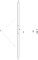
- a length of laminated high temperature superconductor (HTS) wire 100 includes an HTS insert (shown in FIGS. 2-5 ) that is laminated with a lamination material as is described in later sections of this description.
- the laminated HTS wire 100 includes a segment 103 where a material defect in the HTS insert has been addressed by a patching method.
- the patched segment 103 that results from the patching method has a thickness that is less than the wire thickness that results from external splicing methods.
- FIG. 2 shows a lengthwise cross section of a primary HTS insert 200 including a material defect 202.
- the primary HTS insert 200 which runs through the entire length of the laminated HTS wire 100 includes a substrate layer 208, a buffer layer 206, and a superconducting layer 204.
- the superconducting layer 204 is typically made of a crystalline material such as polycrystalline rare-earth/alkaline-earth/metal oxide.
- the material can be yttrium-barium-copper-oxide (YBCO).
- the current-carrying capability of the superconducting layer 204 relies on the quality of the crystalline alignment of the superconducting material.
- a highly aligned superconducting layer 204 is created by first forming the buffer layer 206 on the substrate layer 208 such that the buffer layer's surface has a high degree of crystallographic texture.
- the superconducting layer 204 is then formed by growing a thin layer of superconducting material epitaxially on the buffer layer 206.
- the high degree of crystallographic texture of the buffer layer's surface imparts a high degree of crystalline alignment in the superconducting layer 204.
- HTS inserts fabricated according to the previously described method are commonly referred to as second generation HTS inserts.
- second generation HTS inserts For a more complete description of the fabrication process and the properties of second generation HTS inserts see Otto et al., US Patent Application Publication No. US 2009/0298696 A1 .
- material defects 202 are inadvertently introduced into HTS inserts during the formation of HTS inserts and the fabrication of the HTS wires. Some common material defects are structural defects (e.g., fractures, dimples, etc) and crystallographic defects (e.g., poor crystallographic orientation in the superconducting layer 204). The physical dimensions of material defects 202 are constrained only by physical dimensions of the HTS insert.
- One approach to avoiding such a reduction is to bypass the material defect 202 in the superconducting layer 204 of the primary HTS insert 200 before the primary HTS insert 200 is laminated and without cutting the primary HTS insert 200.
- the material defect 202 in the primary HTS insert 200 is detected. For example, during the HTS insert fabrication process, the resistance of segments of the HTS insert is measured and segments that have a resistance greater than a predetermined value are marked as defective.
- FIG. 3 shows a lengthwise cross section of the primary HTS insert 200 and an HTS insert patch 310.
- the aforementioned defect detection process has located the material defect 202 on the primary HTS insert 200.
- the next step involves creating the HTS insert patch 310 and positioning the patch such that it overlaps the material defect 202.
- the HTS insert patch 310 is formed of the same type of HTS insert as the primary HTS insert 200.
- the HTS insert patch 310 has a width that is equal to the width of the primary HTS insert 200 and a length that is greater than the length L d of the material defect 202.
- the HTS insert patch 310 is then positioned such that it overlaps the material defect 202. Since the second generation HTS inserts used in the present embodiment are asymmetrical, the patch 310 is flipped over so that its superconducting layer 312 is opposite the superconducting layer 204 of the primary HTS insert 200. This orientation facilitates current flowing through the two superconducting layers 204, 312.
- a bonding process establishes an electrical connection between the superconducting layer 204 of the primary HTS insert 200 and the superconducting layer 312 of the HTS insert patch 310 such that current can flow freely between the two layers.
- the bonding process is a soldering process that deposits a layer of solder 414 over the HTS insert patch 310 and in the area between the HTS insert patch 310 and the primary HTS insert 200.
- the solder layer 414 can include any low resistance solder material, for example, indium, Pb-Sn, or Pb-Sn-Ag.
- FIG. 5 shows a lengthwise cross section of the finished HTS wire 500 that is created by depositing a laminating layer 516 onto the patched primary HTS insert 200.
- the lamination layer 516 surrounds the primary HTS insert 200 and the patched segment, including the bonded HTS insert patch 310.
- the lamination layer 516 is a conductive material such as stainless steel or brass. In the event of a fault in the superconducting wire 500, the conductive lamination layer 516 can continue to transmit power.
- the length of the HTS insert patch 310 was greater than the length L d of the material defect 202. However, in some examples, the length of the HTS insert patch 310 is equal to or lesser than the length L d of the material defect 202.
- the HTS insert patch 310 spans the length of the material defect 202. In other examples, the HTS insert patch 310 may only partially cover the material defect 202.
- the lamination material is electrically conductive. In other examples, the lamination material is electrically insulative.
- the HTS insert patching method is carried out prior to the lamination process.
- a defect can be detected in an already laminated wire and the method can involve removing the lamination material in the area of the defect, patching the defect, and then re-laminating in the area of the patch.
- the HTS insert patch 310 has a width that is equal to the width of the material defect 202. In other examples, an HTS insert patch 310 with a smaller width can be used.
Landscapes
- Engineering & Computer Science (AREA)
- Manufacturing & Machinery (AREA)
- Superconductors And Manufacturing Methods Therefor (AREA)
Claims (10)
- Erzeugnis zum Leiten von Strom, wobei das Erzeugnis Folgendes umfasst:ein erstes Segment (103) eines supraleitenden Hochtemperaturdrahtes (100), das einen Defekt (202) aufweist;ein Reparaturstück (310), das Folgendes umfasst:ein zweites Segment eines supraleitenden Hochtemperaturdrahtes, das so positioniert ist, dass es den Defekt überlappt;eine Bondschicht (414), die zwischen dem ersten Segment eines supraleitenden Hochtemperaturdrahtes und dem zweites Segment eines supraleitenden Hochtemperaturdrahtes angeordnet ist;wobei die Bondschicht einen Pfad bildet, dergestalt, dass Strom durch das zweite Segment eines supraleitenden Hochtemperaturdrahtes fließt; unddadurch gekennzeichnet, dass es des Weiteren eine Laminierungsstruktur umfasst, die das erste Segment eines supraleitenden Hochtemperaturdrahtes und das Reparaturstück umgibt.
- Erzeugnis nach Anspruch 1, wobei das erste Segment eines supraleitenden Hochtemperaturdrahtes einen ersten Widerstand aufweist, das zweite Segment eines supraleitenden Hochtemperaturdrahtes einen zweiten Widerstand aufweist und der Wert des zweiten Widerstandes niedriger ist als der Wert des ersten Widerstandes.
- Erzeugnis nach Anspruch 1, wobei die Bondschicht ein Lot mit niedrigem Widerstand umfasst.
- Erzeugnis nach Anspruch 1, wobei der Defekt eine erste Länge aufweist, das zweite Segment eines supraleitenden Hochtemperaturdrahtes eine zweite Länge aufweist, und die zweite Länge größer ist als die erste Länge.
- Erzeugnis nach Anspruch 4, wobei sich das zweite Segment eines supraleitenden Hochtemperaturdrahtes über die Länge des Defekts erstreckt.
- Erzeugnis nach Anspruch 1, wobei der Defekt eine erste Länge aufweist, das zweite Segment eines supraleitenden Hochtemperaturdrahtes eine zweite Länge aufweist und die zweite Länge nicht größer ist als die erste Länge.
- Erzeugnis nach Anspruch 1, wobei die Laminierungsstruktur in elektrischem Kontakt mit dem ersten und dem zweiten Segment eines supraleitenden Hochtemperaturdrahtes steht.
- Erzeugnis nach Anspruch 1, wobei das zweite Segment eines supraleitenden Hochtemperaturdrahtes so ausgebildet ist, dass es eine Länge aufweist, die größer ist als die Länge des Materialabschnitts, der den Defekt enthält.
- Erzeugnis nach Anspruch 1, wobei sich das zweite Segment eines supraleitenden Hochtemperaturdrahtes über den Materialabschnitt erstreckt, der den Defekt enthält.
- Erzeugnis nach Anspruch 1, wobei das zweite Segment eines supraleitenden Hochtemperaturdrahtes so ausgebildet ist, dass es eine Länge aufweist, die nicht größer ist als die Länge des Abschnitts des defekten Materials.
Applications Claiming Priority (2)
| Application Number | Priority Date | Filing Date | Title |
|---|---|---|---|
| US201161454811P | 2011-03-21 | 2011-03-21 | |
| PCT/US2012/028168 WO2012128954A1 (en) | 2011-03-21 | 2012-03-08 | Mitigating the effects of defects in high temperature superconducting wires |
Publications (2)
| Publication Number | Publication Date |
|---|---|
| EP2689477A1 EP2689477A1 (de) | 2014-01-29 |
| EP2689477B1 true EP2689477B1 (de) | 2019-06-19 |
Family
ID=45937558
Family Applications (1)
| Application Number | Title | Priority Date | Filing Date |
|---|---|---|---|
| EP12713433.6A Active EP2689477B1 (de) | 2011-03-21 | 2012-03-08 | Verminderung der auswirkung von defekten bei hochtemperatur-supraleitenden drähten |
Country Status (5)
| Country | Link |
|---|---|
| US (1) | US8680015B2 (de) |
| EP (1) | EP2689477B1 (de) |
| KR (1) | KR101481777B1 (de) |
| ES (1) | ES2739277T3 (de) |
| WO (1) | WO2012128954A1 (de) |
Families Citing this family (4)
| Publication number | Priority date | Publication date | Assignee | Title |
|---|---|---|---|---|
| EP2835838B1 (de) | 2013-08-08 | 2017-02-15 | Theva Dünnschichttechnik GmbH | Hochtemperatur-Supraleiter-Bandleitersystem |
| KR101690421B1 (ko) * | 2015-07-21 | 2017-01-09 | 두산중공업 주식회사 | 고온초전도 선재 결함 수선 장치 및 방법 |
| EP4246602A1 (de) | 2022-03-14 | 2023-09-20 | Theva Dünnschichttechnik GmbH | Hermetisch dichter hochtemperatursupraleitender bandleiter |
| EP4297110A1 (de) | 2022-06-20 | 2023-12-27 | Theva Dünnschichttechnik GmbH | Armierter hochtemperatursupraleitender bandleiter |
Citations (2)
| Publication number | Priority date | Publication date | Assignee | Title |
|---|---|---|---|---|
| JP2009187743A (ja) * | 2008-02-05 | 2009-08-20 | Chubu Electric Power Co Inc | 超電導テープ線材及び欠陥部の補修方法 |
| EP2490275A1 (de) * | 2011-02-16 | 2012-08-22 | Nexans | Verfahren zur Herstellung eines supraleitfähigen elektrischen Leiters |
Family Cites Families (9)
| Publication number | Priority date | Publication date | Assignee | Title |
|---|---|---|---|---|
| DE3905424C2 (de) | 1989-02-22 | 1994-02-17 | Vacuumschmelze Gmbh | Verfahren zur Herstellung einer supraleitenden Verbindung zwischen oxidischen Supraleitern |
| US5583319A (en) * | 1993-10-21 | 1996-12-10 | Lieurance; Dennis W. | Low resistance superconductor cable splice and splicing method |
| US6159905A (en) * | 1999-06-02 | 2000-12-12 | Buzcek; David M. | Methods for joining high temperature superconducting components with negligible critical current degradation and articles of manufacture in accordance therewith |
| US20060063680A1 (en) | 2002-07-26 | 2006-03-23 | Metal Oxide Technologies, Inc. | System and method for joining superconductivity tape |
| US7071148B1 (en) * | 2005-04-08 | 2006-07-04 | Superpower, Inc. | Joined superconductive articles |
| US8030246B2 (en) * | 2006-07-21 | 2011-10-04 | American Superconductor Corporation | Low resistance splice for high temperature superconductor wires |
| US8195260B2 (en) * | 2008-07-23 | 2012-06-05 | American Superconductor Corporation | Two-sided splice for high temperature superconductor laminated wires |
| US20100019776A1 (en) * | 2008-07-23 | 2010-01-28 | Folts Douglas C | Method for analyzing superconducting wire |
| US8418336B2 (en) * | 2009-07-07 | 2013-04-16 | Roger Michael Bennett | Method and system for repairing the flow-line of corrugated metal pipes |
-
2012
- 2012-03-08 ES ES12713433T patent/ES2739277T3/es active Active
- 2012-03-08 EP EP12713433.6A patent/EP2689477B1/de active Active
- 2012-03-08 KR KR1020137027465A patent/KR101481777B1/ko active Active
- 2012-03-08 US US13/414,811 patent/US8680015B2/en active Active
- 2012-03-08 WO PCT/US2012/028168 patent/WO2012128954A1/en not_active Ceased
Patent Citations (2)
| Publication number | Priority date | Publication date | Assignee | Title |
|---|---|---|---|---|
| JP2009187743A (ja) * | 2008-02-05 | 2009-08-20 | Chubu Electric Power Co Inc | 超電導テープ線材及び欠陥部の補修方法 |
| EP2490275A1 (de) * | 2011-02-16 | 2012-08-22 | Nexans | Verfahren zur Herstellung eines supraleitfähigen elektrischen Leiters |
Also Published As
| Publication number | Publication date |
|---|---|
| ES2739277T3 (es) | 2020-01-30 |
| KR101481777B1 (ko) | 2015-01-12 |
| US20120245035A1 (en) | 2012-09-27 |
| EP2689477A1 (de) | 2014-01-29 |
| WO2012128954A1 (en) | 2012-09-27 |
| KR20140003602A (ko) | 2014-01-09 |
| US8680015B2 (en) | 2014-03-25 |
Similar Documents
| Publication | Publication Date | Title |
|---|---|---|
| CA2603768C (en) | Joined superconductive articles | |
| JP4845040B2 (ja) | 薄膜超電導線の接続方法及びその接続構造体 | |
| JP5597711B2 (ja) | マルチフィラメント導体およびその製造方法 | |
| EP2728591B1 (de) | Supraleitendes drahtmaterial, verbindungsstruktur für supraleitendes drahtmaterial, verbindungsverfahren für supraleitendes drahtmaterial und behandlungsverfahren für supraleitendes drahtmaterialende | |
| EP2945168B1 (de) | Supraleitender oxiddraht, verbindungsstruktur dafür und supraleitende vorrichtung | |
| EP2689477B1 (de) | Verminderung der auswirkung von defekten bei hochtemperatur-supraleitenden drähten | |
| CN110770925B (zh) | 提高工程电流密度的高温超导导线 | |
| TW201108257A (en) | Shielded electrical cable | |
| KR102683995B1 (ko) | 제2세대 초전도성 필라멘트와 케이블 | |
| CN103688316A (zh) | 超导线的连接构造、超导线的连接方法以及连接用超导线 | |
| US11877521B2 (en) | Flexible multi-filament high temperature superconducting cable | |
| CN114144850B (zh) | 超导线材的制造 | |
| US10734138B2 (en) | Multi-filament superconducting composites | |
| CN112614623A (zh) | 一种二代高温超导堆叠导体的长线化接线方法 | |
| JP5205558B2 (ja) | 超電導線材、超電導導体および超電導ケーブル | |
| EP2490272B1 (de) | Supraleitendes Element mit länglicher Öffnung und Verfahren zu seiner Herstellung | |
| JP6101490B2 (ja) | 酸化物超電導線材の接続構造体及び超電導機器 | |
| Bascuñán et al. | On the 600 MHz HTS insert for a 1.3 GHz NMR magnet | |
| JP5775785B2 (ja) | 酸化物超電導線材及びその製造方法 | |
| US7417192B2 (en) | Superconductor components | |
| KR20170034197A (ko) | 고온 초전도 선재의 결함 보수 방법 및 고온 초전도 선재의 제조 방법 | |
| KR20150061493A (ko) | 초전도 박막 선재를 이용한 다심 초전도 박막 선재 |
Legal Events
| Date | Code | Title | Description |
|---|---|---|---|
| PUAI | Public reference made under article 153(3) epc to a published international application that has entered the european phase |
Free format text: ORIGINAL CODE: 0009012 |
|
| 17P | Request for examination filed |
Effective date: 20131016 |
|
| AK | Designated contracting states |
Kind code of ref document: A1 Designated state(s): AL AT BE BG CH CY CZ DE DK EE ES FI FR GB GR HR HU IE IS IT LI LT LU LV MC MK MT NL NO PL PT RO RS SE SI SK SM TR |
|
| DAX | Request for extension of the european patent (deleted) | ||
| REG | Reference to a national code |
Ref country code: DE Ref legal event code: R079 Ref document number: 602012061134 Country of ref document: DE Free format text: PREVIOUS MAIN CLASS: H01L0039140000 Ipc: H01L0039020000 |
|
| RIC1 | Information provided on ipc code assigned before grant |
Ipc: H01L 39/02 20060101AFI20160729BHEP Ipc: H01L 39/24 20060101ALI20160729BHEP |
|
| 17Q | First examination report despatched |
Effective date: 20160825 |
|
| STAA | Information on the status of an ep patent application or granted ep patent |
Free format text: STATUS: EXAMINATION IS IN PROGRESS |
|
| GRAP | Despatch of communication of intention to grant a patent |
Free format text: ORIGINAL CODE: EPIDOSNIGR1 |
|
| STAA | Information on the status of an ep patent application or granted ep patent |
Free format text: STATUS: GRANT OF PATENT IS INTENDED |
|
| INTG | Intention to grant announced |
Effective date: 20190117 |
|
| GRAS | Grant fee paid |
Free format text: ORIGINAL CODE: EPIDOSNIGR3 |
|
| GRAA | (expected) grant |
Free format text: ORIGINAL CODE: 0009210 |
|
| STAA | Information on the status of an ep patent application or granted ep patent |
Free format text: STATUS: THE PATENT HAS BEEN GRANTED |
|
| AK | Designated contracting states |
Kind code of ref document: B1 Designated state(s): AL AT BE BG CH CY CZ DE DK EE ES FI FR GB GR HR HU IE IS IT LI LT LU LV MC MK MT NL NO PL PT RO RS SE SI SK SM TR |
|
| REG | Reference to a national code |
Ref country code: GB Ref legal event code: FG4D |
|
| REG | Reference to a national code |
Ref country code: CH Ref legal event code: EP |
|
| REG | Reference to a national code |
Ref country code: IE Ref legal event code: FG4D |
|
| REG | Reference to a national code |
Ref country code: DE Ref legal event code: R096 Ref document number: 602012061134 Country of ref document: DE |
|
| REG | Reference to a national code |
Ref country code: AT Ref legal event code: REF Ref document number: 1146622 Country of ref document: AT Kind code of ref document: T Effective date: 20190715 |
|
| REG | Reference to a national code |
Ref country code: NL Ref legal event code: MP Effective date: 20190619 |
|
| PG25 | Lapsed in a contracting state [announced via postgrant information from national office to epo] |
Ref country code: NO Free format text: LAPSE BECAUSE OF FAILURE TO SUBMIT A TRANSLATION OF THE DESCRIPTION OR TO PAY THE FEE WITHIN THE PRESCRIBED TIME-LIMIT Effective date: 20190919 Ref country code: HR Free format text: LAPSE BECAUSE OF FAILURE TO SUBMIT A TRANSLATION OF THE DESCRIPTION OR TO PAY THE FEE WITHIN THE PRESCRIBED TIME-LIMIT Effective date: 20190619 Ref country code: LT Free format text: LAPSE BECAUSE OF FAILURE TO SUBMIT A TRANSLATION OF THE DESCRIPTION OR TO PAY THE FEE WITHIN THE PRESCRIBED TIME-LIMIT Effective date: 20190619 Ref country code: AL Free format text: LAPSE BECAUSE OF FAILURE TO SUBMIT A TRANSLATION OF THE DESCRIPTION OR TO PAY THE FEE WITHIN THE PRESCRIBED TIME-LIMIT Effective date: 20190619 Ref country code: SE Free format text: LAPSE BECAUSE OF FAILURE TO SUBMIT A TRANSLATION OF THE DESCRIPTION OR TO PAY THE FEE WITHIN THE PRESCRIBED TIME-LIMIT Effective date: 20190619 Ref country code: FI Free format text: LAPSE BECAUSE OF FAILURE TO SUBMIT A TRANSLATION OF THE DESCRIPTION OR TO PAY THE FEE WITHIN THE PRESCRIBED TIME-LIMIT Effective date: 20190619 |
|
| REG | Reference to a national code |
Ref country code: LT Ref legal event code: MG4D |
|
| PG25 | Lapsed in a contracting state [announced via postgrant information from national office to epo] |
Ref country code: BG Free format text: LAPSE BECAUSE OF FAILURE TO SUBMIT A TRANSLATION OF THE DESCRIPTION OR TO PAY THE FEE WITHIN THE PRESCRIBED TIME-LIMIT Effective date: 20190919 Ref country code: LV Free format text: LAPSE BECAUSE OF FAILURE TO SUBMIT A TRANSLATION OF THE DESCRIPTION OR TO PAY THE FEE WITHIN THE PRESCRIBED TIME-LIMIT Effective date: 20190619 Ref country code: RS Free format text: LAPSE BECAUSE OF FAILURE TO SUBMIT A TRANSLATION OF THE DESCRIPTION OR TO PAY THE FEE WITHIN THE PRESCRIBED TIME-LIMIT Effective date: 20190619 Ref country code: GR Free format text: LAPSE BECAUSE OF FAILURE TO SUBMIT A TRANSLATION OF THE DESCRIPTION OR TO PAY THE FEE WITHIN THE PRESCRIBED TIME-LIMIT Effective date: 20190920 |
|
| REG | Reference to a national code |
Ref country code: AT Ref legal event code: MK05 Ref document number: 1146622 Country of ref document: AT Kind code of ref document: T Effective date: 20190619 |
|
| REG | Reference to a national code |
Ref country code: ES Ref legal event code: FG2A Ref document number: 2739277 Country of ref document: ES Kind code of ref document: T3 Effective date: 20200130 |
|
| PG25 | Lapsed in a contracting state [announced via postgrant information from national office to epo] |
Ref country code: PT Free format text: LAPSE BECAUSE OF FAILURE TO SUBMIT A TRANSLATION OF THE DESCRIPTION OR TO PAY THE FEE WITHIN THE PRESCRIBED TIME-LIMIT Effective date: 20191021 Ref country code: SK Free format text: LAPSE BECAUSE OF FAILURE TO SUBMIT A TRANSLATION OF THE DESCRIPTION OR TO PAY THE FEE WITHIN THE PRESCRIBED TIME-LIMIT Effective date: 20190619 Ref country code: NL Free format text: LAPSE BECAUSE OF FAILURE TO SUBMIT A TRANSLATION OF THE DESCRIPTION OR TO PAY THE FEE WITHIN THE PRESCRIBED TIME-LIMIT Effective date: 20190619 Ref country code: CZ Free format text: LAPSE BECAUSE OF FAILURE TO SUBMIT A TRANSLATION OF THE DESCRIPTION OR TO PAY THE FEE WITHIN THE PRESCRIBED TIME-LIMIT Effective date: 20190619 Ref country code: RO Free format text: LAPSE BECAUSE OF FAILURE TO SUBMIT A TRANSLATION OF THE DESCRIPTION OR TO PAY THE FEE WITHIN THE PRESCRIBED TIME-LIMIT Effective date: 20190619 Ref country code: EE Free format text: LAPSE BECAUSE OF FAILURE TO SUBMIT A TRANSLATION OF THE DESCRIPTION OR TO PAY THE FEE WITHIN THE PRESCRIBED TIME-LIMIT Effective date: 20190619 Ref country code: AT Free format text: LAPSE BECAUSE OF FAILURE TO SUBMIT A TRANSLATION OF THE DESCRIPTION OR TO PAY THE FEE WITHIN THE PRESCRIBED TIME-LIMIT Effective date: 20190619 |
|
| PG25 | Lapsed in a contracting state [announced via postgrant information from national office to epo] |
Ref country code: SM Free format text: LAPSE BECAUSE OF FAILURE TO SUBMIT A TRANSLATION OF THE DESCRIPTION OR TO PAY THE FEE WITHIN THE PRESCRIBED TIME-LIMIT Effective date: 20190619 Ref country code: IS Free format text: LAPSE BECAUSE OF FAILURE TO SUBMIT A TRANSLATION OF THE DESCRIPTION OR TO PAY THE FEE WITHIN THE PRESCRIBED TIME-LIMIT Effective date: 20191019 |
|
| PG25 | Lapsed in a contracting state [announced via postgrant information from national office to epo] |
Ref country code: TR Free format text: LAPSE BECAUSE OF FAILURE TO SUBMIT A TRANSLATION OF THE DESCRIPTION OR TO PAY THE FEE WITHIN THE PRESCRIBED TIME-LIMIT Effective date: 20190619 |
|
| PG25 | Lapsed in a contracting state [announced via postgrant information from national office to epo] |
Ref country code: DK Free format text: LAPSE BECAUSE OF FAILURE TO SUBMIT A TRANSLATION OF THE DESCRIPTION OR TO PAY THE FEE WITHIN THE PRESCRIBED TIME-LIMIT Effective date: 20190619 Ref country code: PL Free format text: LAPSE BECAUSE OF FAILURE TO SUBMIT A TRANSLATION OF THE DESCRIPTION OR TO PAY THE FEE WITHIN THE PRESCRIBED TIME-LIMIT Effective date: 20190619 |
|
| PG25 | Lapsed in a contracting state [announced via postgrant information from national office to epo] |
Ref country code: IS Free format text: LAPSE BECAUSE OF FAILURE TO SUBMIT A TRANSLATION OF THE DESCRIPTION OR TO PAY THE FEE WITHIN THE PRESCRIBED TIME-LIMIT Effective date: 20200224 |
|
| REG | Reference to a national code |
Ref country code: DE Ref legal event code: R097 Ref document number: 602012061134 Country of ref document: DE |
|
| PLBE | No opposition filed within time limit |
Free format text: ORIGINAL CODE: 0009261 |
|
| STAA | Information on the status of an ep patent application or granted ep patent |
Free format text: STATUS: NO OPPOSITION FILED WITHIN TIME LIMIT |
|
| PG2D | Information on lapse in contracting state deleted |
Ref country code: IS |
|
| 26N | No opposition filed |
Effective date: 20200603 |
|
| PG25 | Lapsed in a contracting state [announced via postgrant information from national office to epo] |
Ref country code: SI Free format text: LAPSE BECAUSE OF FAILURE TO SUBMIT A TRANSLATION OF THE DESCRIPTION OR TO PAY THE FEE WITHIN THE PRESCRIBED TIME-LIMIT Effective date: 20190619 |
|
| PG25 | Lapsed in a contracting state [announced via postgrant information from national office to epo] |
Ref country code: MC Free format text: LAPSE BECAUSE OF FAILURE TO SUBMIT A TRANSLATION OF THE DESCRIPTION OR TO PAY THE FEE WITHIN THE PRESCRIBED TIME-LIMIT Effective date: 20190619 |
|
| REG | Reference to a national code |
Ref country code: CH Ref legal event code: PL |
|
| REG | Reference to a national code |
Ref country code: BE Ref legal event code: MM Effective date: 20200331 |
|
| PG25 | Lapsed in a contracting state [announced via postgrant information from national office to epo] |
Ref country code: LU Free format text: LAPSE BECAUSE OF NON-PAYMENT OF DUE FEES Effective date: 20200308 |
|
| PG25 | Lapsed in a contracting state [announced via postgrant information from national office to epo] |
Ref country code: LI Free format text: LAPSE BECAUSE OF NON-PAYMENT OF DUE FEES Effective date: 20200331 Ref country code: IE Free format text: LAPSE BECAUSE OF NON-PAYMENT OF DUE FEES Effective date: 20200308 Ref country code: CH Free format text: LAPSE BECAUSE OF NON-PAYMENT OF DUE FEES Effective date: 20200331 |
|
| PG25 | Lapsed in a contracting state [announced via postgrant information from national office to epo] |
Ref country code: BE Free format text: LAPSE BECAUSE OF NON-PAYMENT OF DUE FEES Effective date: 20200331 |
|
| PG25 | Lapsed in a contracting state [announced via postgrant information from national office to epo] |
Ref country code: MT Free format text: LAPSE BECAUSE OF FAILURE TO SUBMIT A TRANSLATION OF THE DESCRIPTION OR TO PAY THE FEE WITHIN THE PRESCRIBED TIME-LIMIT Effective date: 20190619 Ref country code: CY Free format text: LAPSE BECAUSE OF FAILURE TO SUBMIT A TRANSLATION OF THE DESCRIPTION OR TO PAY THE FEE WITHIN THE PRESCRIBED TIME-LIMIT Effective date: 20190619 |
|
| PG25 | Lapsed in a contracting state [announced via postgrant information from national office to epo] |
Ref country code: MK Free format text: LAPSE BECAUSE OF FAILURE TO SUBMIT A TRANSLATION OF THE DESCRIPTION OR TO PAY THE FEE WITHIN THE PRESCRIBED TIME-LIMIT Effective date: 20190619 |
|
| REG | Reference to a national code |
Ref country code: DE Ref legal event code: R079 Ref document number: 602012061134 Country of ref document: DE Free format text: PREVIOUS MAIN CLASS: H01L0039020000 Ipc: H10N0060800000 |
|
| PGFP | Annual fee paid to national office [announced via postgrant information from national office to epo] |
Ref country code: IT Payment date: 20230321 Year of fee payment: 12 |
|
| PGFP | Annual fee paid to national office [announced via postgrant information from national office to epo] |
Ref country code: ES Payment date: 20230403 Year of fee payment: 12 |
|
| P01 | Opt-out of the competence of the unified patent court (upc) registered |
Effective date: 20230810 |
|
| PG25 | Lapsed in a contracting state [announced via postgrant information from national office to epo] |
Ref country code: IT Free format text: LAPSE BECAUSE OF NON-PAYMENT OF DUE FEES Effective date: 20240308 |
|
| REG | Reference to a national code |
Ref country code: ES Ref legal event code: FD2A Effective date: 20250429 |
|
| PG25 | Lapsed in a contracting state [announced via postgrant information from national office to epo] |
Ref country code: ES Free format text: LAPSE BECAUSE OF NON-PAYMENT OF DUE FEES Effective date: 20240309 |
|
| PGFP | Annual fee paid to national office [announced via postgrant information from national office to epo] |
Ref country code: GB Payment date: 20260327 Year of fee payment: 15 |
|
| PGFP | Annual fee paid to national office [announced via postgrant information from national office to epo] |
Ref country code: DE Payment date: 20260327 Year of fee payment: 15 |
|
| PGFP | Annual fee paid to national office [announced via postgrant information from national office to epo] |
Ref country code: FR Payment date: 20260325 Year of fee payment: 15 |