EP2676321B1 - Kupplungsanordnung - Google Patents
Kupplungsanordnung Download PDFInfo
- Publication number
- EP2676321B1 EP2676321B1 EP11867472.0A EP11867472A EP2676321B1 EP 2676321 B1 EP2676321 B1 EP 2676321B1 EP 11867472 A EP11867472 A EP 11867472A EP 2676321 B1 EP2676321 B1 EP 2676321B1
- Authority
- EP
- European Patent Office
- Prior art keywords
- module
- slot
- substrate
- motherboard
- conductor
- Prior art date
- Legal status (The legal status is an assumption and is not a legal conclusion. Google has not performed a legal analysis and makes no representation as to the accuracy of the status listed.)
- Active
Links
Images


Classifications
-
- H—ELECTRICITY
- H01—ELECTRIC ELEMENTS
- H01P—WAVEGUIDES; RESONATORS, LINES, OR OTHER DEVICES OF THE WAVEGUIDE TYPE
- H01P5/00—Coupling devices of the waveguide type
- H01P5/08—Coupling devices of the waveguide type for linking dissimilar lines or devices
- H01P5/10—Coupling devices of the waveguide type for linking dissimilar lines or devices for coupling balanced lines or devices with unbalanced lines or devices
- H01P5/107—Hollow-waveguide/strip-line transitions
-
- H—ELECTRICITY
- H01—ELECTRIC ELEMENTS
- H01P—WAVEGUIDES; RESONATORS, LINES, OR OTHER DEVICES OF THE WAVEGUIDE TYPE
- H01P5/00—Coupling devices of the waveguide type
- H01P5/08—Coupling devices of the waveguide type for linking dissimilar lines or devices
-
- H—ELECTRICITY
- H01—ELECTRIC ELEMENTS
- H01P—WAVEGUIDES; RESONATORS, LINES, OR OTHER DEVICES OF THE WAVEGUIDE TYPE
- H01P5/00—Coupling devices of the waveguide type
- H01P5/02—Coupling devices of the waveguide type with invariable factor of coupling
- H01P5/022—Transitions between lines of the same kind and shape, but with different dimensions
- H01P5/028—Transitions between lines of the same kind and shape, but with different dimensions between strip lines
Definitions
- the invention relates to a coupling arrangement for a transfer of a microwave signal between a motherboard and a module.
- SMT Surface Mount
- modules for microwave radio system may be desired to be connected to a motherboard.
- a package which may contain some kind of microwave electronics such as a filter or a microwave integrated circuit.
- Another type of module may be a smaller (sub-)board carrying several electrical components. All such modules, however, have in common that they must be connected to the main motherboard in such a way that microwave signals can be exchanged between them in an efficient way.
- SMT surface mounted
- Chip On Board (COB) solutions mostly is used, i.e. the chip is directly mounted on and electrically interconnected to its final circuit board, instead of first being incorporated in a package that then can be mounted on a desired board.
- COB Chip On Board
- the chip on board model means higher technology in the end manufacturing and such solutions are also harder and more expensive to repair.
- Chip On Board concepts allow full Surface Mount (SMT)-manufacturing of products that can transfer microwave signals with a frequency of up to around 120 GHz.
- SMT Surface Mount
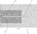
- Such a prior art coupling arrangement 1 is shown in fig. 1 . It discloses a motherboard 2 comprising a substrate 3 and a microstrip 4. The motherboard 2 is connected to a surface mount module 5, said module comprising a substrate 6 and a microstrip conductor 7. The connection 17 between the motherboard 2 and the module 5 is shown encircled with an oval in the figure. A via-hole 18 is shown interconnecting an underside with an upper side of the substrate 6 of the module 5.
- X-X denotes a cross section through the connection 17; this cross section is detailed in fig. 2 .
- the cross section X-X of the connection between the motherboard and the module can be studied further in fig. 2 .
- the motherboard 2 is connected to the module 5 via a coplanar waveguide 20.
- the coplanar waveguide 20 comprises two ground conductors 21 each comprising a solder pad on each of the motherboard and the module with solder in between. The ground can be seen transported from the motherboard ground plane 19 through the motherboard, by way of vias 22, to the upper side of the motherboard.
- the coplanar waveguide 20 further comprises, in the same plane as the ground conductors 21, a signal conductor 23 comprising the microstrip on the motherboard connected with solder to a via-hole 18 leading up to the microstrip 7 on the upper side of the module 5.
- Tze-Min Shen et al. do not disclose a slot coupling comprising two slots which are connected by a connecting substance around their peripheries.
- US 5821836 A relates to miniaturized or micromachined circuits, and more specifically to filters and multiplexers that provide improved performance for high frequency applications.
- WO 2011/030277 A2 relates to a system for injecting and guiding millimeter- waves through a Printed Circuit Board (PCB), the system including at least two laminas belonging to a PCB.
- An electrically conductive plating is applied on the insulating walls of a cavity formed perpendicularly through the laminas.
- a probe located above the cavity is printed on a lamina belonging to the PCB.
- the cavity guides millimeter-waves injected by the probe at one side of the cavity to the other side of the cavity.
- SIWs Substrate Integrated Waveguides
- a flexible PCB for application in the 77-81 GHz range.
- Vertical walls of the SIWs consist of multiple electrodeposited metallic wires, diameters of these wires and the spacing between them being on the order of hundreds of nanometers.
- US 6437669 B1 relates generally to microwave and millimeter wave substrate technology and, more particularly, to a method for forming microwave and millimeter wave frequency solder connections to a substrate.
- a main object is consequently to provide a coupling arrangement for a surface mounted device module that is suitable for transfer of signals with a high frequency.
- This object is attained with a slot-feed technology for input/output transmit signals to/from the module from/to the motherboard. This will give less loss than existing systems.
- the coupling arrangement 1, for transfer of a microwave signal, according to the invention comprises:
- SMD Surface Mount Device
- FIG. 3 depicts a coupling arrangement 1 for transfer of a microwave signal according to the invention.
- the arrangement 1 comprises a motherboard 2 comprising a substrate 3 with a microstrip conductor 4, and a module 5 comprising a substrate 6 with a microstrip conductor 7.
- the module 5 is attached to the motherboard 2 such that the motherboard conductor 4 by means of a connection 17 is in electrical contact with the module conductor 7, whereby the microwave signal may be transferred between the motherboard conductor 4 and the module conductor 7.
- the connection 17 comprises the motherboard conductor 4 connected to a substrate integrated waveguide 8 on the motherboard 2, which substrate integrated waveguide 8 is connected to the module conductor 7 via a slot coupling 9.
- a substrate integrated waveguide is an electromagnetic waveguide formed in a dielectric substrate by forming metalized trenches or densely arranging metalized via-holes connecting upper and lower metal planes of the substrate. These trenches or via-holes correspond to the metal walls of an ordinary hollow electromagnetic waveguide.
- a slot coupling is a coupling that transmits electromagnetic waves from one place to another by means of an opening or slot in an electrically conductive layer.
- the slot allows electromagnetic waves to escape from the layer and to radiate away from it.
- Such slots have ordinarily been used in for instance the feeding of patch antennas.
- the aperture slot can be of different sizes and shape and these design parameters drive the bandwidth i.e. these parameters have an impact on the frequency content of the signal transmitted through the slot.
- Fig. 4 depicts the motherboard 2 from the side which is facing the module 5 in fig. 3 .
- the connection described in fig. 3 entails the microstrip conductor 4 connected to the substrate integrated waveguide 8.
- the substrate integrated waveguide 8 comprises, in the same way as the microstrip conductor 4, a thin layer or foil 24 of electrically conducting material coated on the substrate of the motherboard.
- the substrate integrated waveguide 8 further comprises trenches 25 that are plated with an electrically conducting material. Alternatively, the trenches 25 could be plated via-holes that are positioned at appropriate distances from each other in dependence on the frequency of the signal that is to be transmitted. In fig.
- the trenches are elongated rectangles that are formed all around the foil 24 except on the left hand of the figure where the microstrip 4 enters the substrate integrated waveguide.
- the trenches 25 run through the substrate of the motherboard 2 and are in electrical contact with a ground plane on the other side of the motherboard (not shown in fig. 4 ).
- the side of the module 5 which is facing the side of the motherboard in fig. 4 is shown. It comprises a ground plane 12 with an open slot 11 in it.
- the microstrip conductor 7 of the module, situated on the side opposite of the ground plane 12 is shown as a dashed rectangle.
- the slot coupling 9 comprises a slot 10 in the substrate integrated waveguide 8 connected to a slot 11 in a ground plane 12 on a side of the module substrate 6.
- the two slots 10, 11 are connected by a connecting substance 14 (see fig. 3 ) around their peripheries. This connection should be as thin as possible, as otherwise the slot will have waveguide properties, deteriorating performance.
- the module conductor 7 is situated opposite the ground plane slot 11 on a side of the module substrate 6 opposite the side with the ground plane 12.
- a microwave signal entering a microstrip 4 can be led into the substrate integrated waveguide 8, transferred via the slot coupling 9 (comprising the slots 10, 11 and the connecting substance 14) and feed the microstrip 7 of the module 5.
- the reverse order, leading a signal from the microstrip 7 to the microstrip 4 is equivalently possible.
- the slots 10 and 11 are aligned with each other.
- a coupling arrangement 1 with slots 10, 11 should be assembled with a misalignment of the slots 10, 11, is may be compensated with walls of the connecting substance 14 between the slots 10, 11 that are oblique to a plane in parallel with any of the slots 10, 11.
- the connecting substance will form after the top and bottom "solder-pads"
- the walls of the connecting substance part of the waveguide will compensate some "mismatch" by stretching obliquely between slots.
- the connecting substance 14 connecting the slots 10, 11 may be solder, which probably would be the normal case.
- other electrically conducting substances such as electrically conducting adhesive are also possible.
- a small space 16 can be seen within the slot coupling 9.
- space 16 can be provided with a dielectric material instead of air. In this way, a better adaptation of the transition from the substrate of the motherboard to the substrate of the module or vice versa can be obtained, which would lessen the amount of reflections of a microwave signal that traverses the coupling arrangement.
- a convenient way of applying such dielectric material when the slot coupling is made up of two slots 10, 11 connected to each other, would be printing the dielectric inside of the slot 10 of the substrate integrated waveguide 8.
- the printing of the dielectric could be in the slot 11 of the ground plane 12 of the module 5 or even in both slots 10, 11. Such printing could for instance accomplished by screen printing.
- the dielectric material is printed such that there is a space between the dielectric material and a wall of the slot in which it is printed, there is a margin for misalignment of the slots when they are assembled to form the slot coupling. If the slots are assembled without misalignment, said space may be filled with solder paste, or what ever connecting substance that is used, instead.
- the dielectric material has a relative permittivity within a range of +/- 20% of the permittivity of the substrate of the motherboard or the module, the amount of reflected energy of a microwave signal traversing the coupling arrangement should be quite low. The best performance would be attained if the dielectric and the substrates of the motherboard and the module all have the same permittivity.
- the coupling arrangement 1 according to any of the described embodiments would be provided wherein the module comprises a Microwave Monolithic Integrated Circuit.
- a Microwave Monolithic Integrated Circuit may for instance perform functions on microwave signals, such as mixing, power amplification, low noise amplification and high frequency switching.
- the module may for instance be a surface mount package or a sub-board.
- the invention concurrently also provides for an elegant connection of the ground plane of the motherboard to the ground plane of the module.
Landscapes
- Waveguide Connection Structure (AREA)
- Waveguides (AREA)
Claims (8)
- Kopplungsanordnung (1) zum Transfer eines Mikrowellensignals, wobei die Anordnung (1) Folgendes umfasst:- ein Motherboard (2), das ein Substrat (3) mit einem Mikrostreifenleiter (4) umfasst,- ein Modul (5), das ein Substrat (6) mit einem Mikrostreifenleiter (7) umfasst,- einen in dem Substrat (3) des Motherboards (2) gebildeten integrierten Substrat-Wellenleiter (8) und- eine Schlitzkopplung (9);wobei das Modul (5) so an dem Motherboard (2) angebracht ist, dass sich der Motherboard-Leiter (4) mittels einer Verbindung (17) in elektrischem Kontakt mit dem Modulleiter (7) befindet, wodurch das Mikrowellensignal zwischen dem Motherboard-Leiter (4) und dem Modulleiter (7) transferiert werden kann;
wobei die Verbindung (17) Folgendes umfasst:- den integrierten Substrat-Wellenleiter (8),- die Schlitzkopplung (9),- den Modulleiter (7) und- den Motherboard-Leiter (4), der mit dem integrierten Substrat-Wellenleiter (8) verbunden ist, wobei dieser integrierte Substrat-Wellenleiter (8) über die Schlitzkopplung (9) mit dem Modulleiter (7) verbunden ist;wobei die Schlitzkopplung (9) Folgendes umfasst:- einen Schlitz (11) in einer Massefläche (12) auf einer Seite des Modulsubstrats (6),- einen Schlitz (10) in dem mit dem Schlitz (11) verbundenen integrierten Substrat-Wellenleiter (8) in der Massefläche (12) auf der Seite des Modulsubstrats (6) und- eine verbindende Substanz (14);wobei die zwei Schlitze (10, 11) durch die verbindende Substanz (14) um ihre Peripherien herum verbunden sind, wodurch ein Raum in der Schlitzkopplung (9) gebildet wird; und
wobei sich der Modulleiter (7) gegenüber dem Masseflächenschlitz (11) auf der Seite des Modulsubstrats (6) gegenüber der Seite mit der Massefläche (12) befindet,
wobei der Raum (16) mit einem dielektrischen Material versehen ist,
wobei das dielektrische Material eine relative Permittivität in einem Bereich von +/-20% der Permittivität des Substrats des Motherboards oder des Moduls aufweist. - Kopplungsanordnung (1) nach Anspruch 1, wobei die Schlitze (10, 11) miteinander ausgerichtet sind.
- Kopplungsanordnung (1) nach Anspruch 1, wobei eine Fehlausrichtung der Schlitze (10, 11) mit Wänden der verbindenden Substanz (14) zwischen den Schlitzen (10, 11), die schräg zu einer Ebene parallel mit beliebigen der Schlitze (10, 11) sind, kompensiert wird.
- Kopplungsanordnung (1) nach einem der Ansprüche 1-3, wobei die verbindende Substanz (14), die die Schlitze (10, 11) verbindet, Lot oder elektrisch leitender Kleber ist.
- Kopplungsanordnung (1) nach Anspruch 1, wobei das dielektrische Material im Inneren eines beliebigen von dem Schlitz (10) des integrierten Substrat-Wellenleiters (8) und dem Schlitz (11) der Massefläche (12) des Moduls (5) gedruckt ist.
- Kopplungsanordnung (1) nach Anspruch 5, wobei das dielektrische Material so gedruckt ist, dass ein Raum zwischen dem dielektrischen Material und einer Wand des Schlitzes, worin es gedruckt ist, besteht.
- Kopplungsanordnung (1) nach Anspruch 1, wobei das Modul eine monolithische integrierte Mikrowellenschaltung umfasst.
- Kopplungsanordnung (1) nach Anspruch 1, wobei das Modul eine Oberflächenanbringungs-Kapselung ist.
Applications Claiming Priority (1)
| Application Number | Priority Date | Filing Date | Title |
|---|---|---|---|
| PCT/CN2011/076793 WO2012167465A1 (en) | 2011-07-04 | 2011-07-04 | Coupling arrangement |
Publications (3)
| Publication Number | Publication Date |
|---|---|
| EP2676321A1 EP2676321A1 (de) | 2013-12-25 |
| EP2676321A4 EP2676321A4 (de) | 2014-01-01 |
| EP2676321B1 true EP2676321B1 (de) | 2018-09-05 |
Family
ID=47295357
Family Applications (1)
| Application Number | Title | Priority Date | Filing Date |
|---|---|---|---|
| EP11867472.0A Active EP2676321B1 (de) | 2011-07-04 | 2011-07-04 | Kupplungsanordnung |
Country Status (4)
| Country | Link |
|---|---|
| US (1) | US9252474B2 (de) |
| EP (1) | EP2676321B1 (de) |
| CN (1) | CN103650235B (de) |
| WO (1) | WO2012167465A1 (de) |
Families Citing this family (18)
| Publication number | Priority date | Publication date | Assignee | Title |
|---|---|---|---|---|
| US9011177B2 (en) | 2009-01-30 | 2015-04-21 | Molex Incorporated | High speed bypass cable assembly |
| US9142921B2 (en) | 2013-02-27 | 2015-09-22 | Molex Incorporated | High speed bypass cable for use with backplanes |
| JP6208878B2 (ja) | 2013-09-04 | 2017-10-04 | モレックス エルエルシー | ケーブルバイパスを備えるコネクタシステム |
| JP6417329B2 (ja) * | 2013-10-01 | 2018-11-07 | ソニーセミコンダクタソリューションズ株式会社 | コネクタ装置及び通信システム |
| US10367280B2 (en) | 2015-01-11 | 2019-07-30 | Molex, Llc | Wire to board connectors suitable for use in bypass routing assemblies |
| KR102120813B1 (ko) | 2015-01-11 | 2020-06-17 | 몰렉스 엘엘씨 | 회로 기판 바이패스 조립체 및 그를 위한 구성요소 |
| US9537199B2 (en) * | 2015-03-19 | 2017-01-03 | International Business Machines Corporation | Package structure having an integrated waveguide configured to communicate between first and second integrated circuit chips |
| CN107548480B (zh) | 2015-05-04 | 2020-08-11 | 莫列斯有限公司 | 采用旁路组件的计算设备 |
| EP3091380B1 (de) | 2015-05-05 | 2021-07-07 | Huawei Technologies Co., Ltd. | Anordnung zur optischen kopplung |
| CN105305057B (zh) * | 2015-11-27 | 2018-10-09 | 哈尔滨工业大学 | 一种空气集成波导的馈电结构 |
| US10424878B2 (en) | 2016-01-11 | 2019-09-24 | Molex, Llc | Cable connector assembly |
| KR102092627B1 (ko) * | 2016-01-11 | 2020-03-24 | 몰렉스 엘엘씨 | 루트설정 조립체 및 이를 사용한 시스템 |
| JP6626213B2 (ja) | 2016-01-19 | 2019-12-25 | モレックス エルエルシー | 一体型ルーティングアセンブリ及びそれを用いたシステム |
| RU2703604C1 (ru) * | 2016-02-12 | 2019-10-21 | Телефонактиеболагет Лм Эрикссон (Пабл) | Переходное устройство, содержащее бесконтактный переход или соединение между siw и волноводом или антенной |
| JP6190932B1 (ja) | 2016-08-26 | 2017-08-30 | 株式会社フジクラ | 伝送線路 |
| CN107317081B (zh) * | 2017-07-05 | 2020-11-10 | 电子科技大学 | 太赫兹无跳线倒置共面波导单片电路封装过渡结构 |
| US11139581B2 (en) * | 2019-03-07 | 2021-10-05 | Aptiv Technologies Limited | Signaling device including a slot transition between a substrate integrated waveguide and a signal generator |
| CN113571900B (zh) * | 2021-07-30 | 2024-04-12 | 海信集团控股股份有限公司 | 一种馈电结构、毫米波天线及汽车 |
Family Cites Families (8)
| Publication number | Priority date | Publication date | Assignee | Title |
|---|---|---|---|---|
| US5856911A (en) * | 1996-11-12 | 1999-01-05 | National Semiconductor Corporation | Attachment assembly for integrated circuits |
| US5821836A (en) * | 1997-05-23 | 1998-10-13 | The Regents Of The University Of Michigan | Miniaturized filter assembly |
| SE518572C2 (sv) * | 1997-08-25 | 2002-10-22 | Ericsson Telefon Ab L M | Bärarelement för ett chips samt chipsmodul |
| US6870438B1 (en) * | 1999-11-10 | 2005-03-22 | Kyocera Corporation | Multi-layered wiring board for slot coupling a transmission line to a waveguide |
| US6437669B1 (en) * | 2000-09-29 | 2002-08-20 | Applied Micro Circuits Corporation | Microwave to millimeter wave frequency substrate interface |
| CN1848030A (zh) * | 2005-04-14 | 2006-10-18 | 广达电脑股份有限公司 | 在计算机主机板上制作射频模块的方法 |
| CN101276957B (zh) * | 2008-03-04 | 2012-02-01 | 东南大学 | 基于半模基片集成波导腔体的多阻带超宽带天线 |
| DE112010003585T5 (de) * | 2009-09-08 | 2012-11-22 | Siklu Communication ltd. | Rfic-schnittstellen und millimeterwellenstrukturen |
-
2011
- 2011-07-04 WO PCT/CN2011/076793 patent/WO2012167465A1/en not_active Ceased
- 2011-07-04 CN CN201180072099.0A patent/CN103650235B/zh active Active
- 2011-07-04 EP EP11867472.0A patent/EP2676321B1/de active Active
-
2013
- 2013-12-30 US US14/143,200 patent/US9252474B2/en active Active
Non-Patent Citations (1)
| Title |
|---|
| None * |
Also Published As
| Publication number | Publication date |
|---|---|
| EP2676321A4 (de) | 2014-01-01 |
| US9252474B2 (en) | 2016-02-02 |
| CN103650235A (zh) | 2014-03-19 |
| EP2676321A1 (de) | 2013-12-25 |
| WO2012167465A1 (en) | 2012-12-13 |
| US20140111293A1 (en) | 2014-04-24 |
| CN103650235B (zh) | 2015-03-25 |
Similar Documents
| Publication | Publication Date | Title |
|---|---|---|
| EP2676321B1 (de) | Kupplungsanordnung | |
| EP2979321B1 (de) | Übergang zwischen einer siw und einer wellenleiterschnittstelle | |
| EP2979323B1 (de) | Siw-antennenanordnung | |
| US9577340B2 (en) | Waveguide adapter plate to facilitate accurate alignment of sectioned waveguide channel in microwave antenna assembly | |
| US9515385B2 (en) | Coplanar waveguide implementing launcher and waveguide channel section in IC package substrate | |
| US9419341B2 (en) | RF system-in-package with quasi-coaxial coplanar waveguide transition | |
| EP3252870B1 (de) | Antennenmodul | |
| KR20120105264A (ko) | 데이터 통신 선로 구조 및 데이터 통신 선로 설계 방법 | |
| US9312590B2 (en) | High-frequency signal transmission line and electronic device | |
| CN102709658B (zh) | 一种平衡微带线过渡的半模双脊基片集成波导 | |
| US20230088793A1 (en) | Transition structure between transmission line of multilayer pcb and waveguide | |
| WO2023016024A1 (zh) | 电路板、天线结构及电子设备 | |
| CN102201607A (zh) | 基于ltcc技术的微带-带状线转换 | |
| CN108684139B (zh) | 一种电路板 | |
| US7196274B2 (en) | Multi-layer integrated RF/IF circuit board | |
| CN217507641U (zh) | 一种平面微带转间隙波导天线 | |
| WO2014157031A1 (ja) | 高周波伝送線路、および電子機器 | |
| US7202419B2 (en) | Multi-layer integrated RF/IF circuit board including a central non-conductive layer | |
| JP2002016408A (ja) | 配線基板およびその導波管との接続構造 | |
| CN114867197B (zh) | 射频基板互联结构及射频电子设备 | |
| KR20100005616A (ko) | 손실 개선을 위한 rf 전송 선로 | |
| CN115663439A (zh) | 一种应用于液晶移相器的共面波导至带状线的过渡结构 | |
| US9172126B2 (en) | Module and coupling arrangement | |
| US20260094974A1 (en) | Laminate substrate for a radiofrequency device | |
| US20260096439A1 (en) | Laminate substrate for a radiofrequency device |
Legal Events
| Date | Code | Title | Description |
|---|---|---|---|
| PUAI | Public reference made under article 153(3) epc to a published international application that has entered the european phase |
Free format text: ORIGINAL CODE: 0009012 |
|
| 17P | Request for examination filed |
Effective date: 20130916 |
|
| AK | Designated contracting states |
Kind code of ref document: A1 Designated state(s): AL AT BE BG CH CY CZ DE DK EE ES FI FR GB GR HR HU IE IS IT LI LT LU LV MC MK MT NL NO PL PT RO RS SE SI SK SM TR |
|
| A4 | Supplementary search report drawn up and despatched |
Effective date: 20131128 |
|
| RIC1 | Information provided on ipc code assigned before grant |
Ipc: H01P 3/00 20060101AFI20131122BHEP |
|
| DAX | Request for extension of the european patent (deleted) | ||
| STAA | Information on the status of an ep patent application or granted ep patent |
Free format text: STATUS: EXAMINATION IS IN PROGRESS |
|
| 17Q | First examination report despatched |
Effective date: 20170509 |
|
| REG | Reference to a national code |
Ref country code: DE Ref legal event code: R079 Ref document number: 602011051890 Country of ref document: DE Free format text: PREVIOUS MAIN CLASS: H01P0003000000 Ipc: H01P0005107000 |
|
| GRAP | Despatch of communication of intention to grant a patent |
Free format text: ORIGINAL CODE: EPIDOSNIGR1 |
|
| STAA | Information on the status of an ep patent application or granted ep patent |
Free format text: STATUS: GRANT OF PATENT IS INTENDED |
|
| RIC1 | Information provided on ipc code assigned before grant |
Ipc: H01P 5/08 20060101ALI20180216BHEP Ipc: H01P 5/107 20060101AFI20180216BHEP Ipc: H01P 5/02 20060101ALI20180216BHEP |
|
| INTG | Intention to grant announced |
Effective date: 20180316 |
|
| INTG | Intention to grant announced |
Effective date: 20180316 |
|
| GRAS | Grant fee paid |
Free format text: ORIGINAL CODE: EPIDOSNIGR3 |
|
| GRAA | (expected) grant |
Free format text: ORIGINAL CODE: 0009210 |
|
| STAA | Information on the status of an ep patent application or granted ep patent |
Free format text: STATUS: THE PATENT HAS BEEN GRANTED |
|
| AK | Designated contracting states |
Kind code of ref document: B1 Designated state(s): AL AT BE BG CH CY CZ DE DK EE ES FI FR GB GR HR HU IE IS IT LI LT LU LV MC MK MT NL NO PL PT RO RS SE SI SK SM TR |
|
| REG | Reference to a national code |
Ref country code: GB Ref legal event code: FG4D |
|
| REG | Reference to a national code |
Ref country code: CH Ref legal event code: EP |
|
| REG | Reference to a national code |
Ref country code: AT Ref legal event code: REF Ref document number: 1038924 Country of ref document: AT Kind code of ref document: T Effective date: 20180915 |
|
| REG | Reference to a national code |
Ref country code: IE Ref legal event code: FG4D |
|
| REG | Reference to a national code |
Ref country code: DE Ref legal event code: R096 Ref document number: 602011051890 Country of ref document: DE |
|
| REG | Reference to a national code |
Ref country code: NL Ref legal event code: MP Effective date: 20180905 |
|
| REG | Reference to a national code |
Ref country code: LT Ref legal event code: MG4D |
|
| PG25 | Lapsed in a contracting state [announced via postgrant information from national office to epo] |
Ref country code: LT Free format text: LAPSE BECAUSE OF FAILURE TO SUBMIT A TRANSLATION OF THE DESCRIPTION OR TO PAY THE FEE WITHIN THE PRESCRIBED TIME-LIMIT Effective date: 20180905 Ref country code: RS Free format text: LAPSE BECAUSE OF FAILURE TO SUBMIT A TRANSLATION OF THE DESCRIPTION OR TO PAY THE FEE WITHIN THE PRESCRIBED TIME-LIMIT Effective date: 20180905 Ref country code: NO Free format text: LAPSE BECAUSE OF FAILURE TO SUBMIT A TRANSLATION OF THE DESCRIPTION OR TO PAY THE FEE WITHIN THE PRESCRIBED TIME-LIMIT Effective date: 20181205 Ref country code: BG Free format text: LAPSE BECAUSE OF FAILURE TO SUBMIT A TRANSLATION OF THE DESCRIPTION OR TO PAY THE FEE WITHIN THE PRESCRIBED TIME-LIMIT Effective date: 20181205 Ref country code: GR Free format text: LAPSE BECAUSE OF FAILURE TO SUBMIT A TRANSLATION OF THE DESCRIPTION OR TO PAY THE FEE WITHIN THE PRESCRIBED TIME-LIMIT Effective date: 20181206 Ref country code: FI Free format text: LAPSE BECAUSE OF FAILURE TO SUBMIT A TRANSLATION OF THE DESCRIPTION OR TO PAY THE FEE WITHIN THE PRESCRIBED TIME-LIMIT Effective date: 20180905 Ref country code: SE Free format text: LAPSE BECAUSE OF FAILURE TO SUBMIT A TRANSLATION OF THE DESCRIPTION OR TO PAY THE FEE WITHIN THE PRESCRIBED TIME-LIMIT Effective date: 20180905 |
|
| REG | Reference to a national code |
Ref country code: AT Ref legal event code: MK05 Ref document number: 1038924 Country of ref document: AT Kind code of ref document: T Effective date: 20180905 |
|
| PG25 | Lapsed in a contracting state [announced via postgrant information from national office to epo] |
Ref country code: HR Free format text: LAPSE BECAUSE OF FAILURE TO SUBMIT A TRANSLATION OF THE DESCRIPTION OR TO PAY THE FEE WITHIN THE PRESCRIBED TIME-LIMIT Effective date: 20180905 Ref country code: AL Free format text: LAPSE BECAUSE OF FAILURE TO SUBMIT A TRANSLATION OF THE DESCRIPTION OR TO PAY THE FEE WITHIN THE PRESCRIBED TIME-LIMIT Effective date: 20180905 Ref country code: LV Free format text: LAPSE BECAUSE OF FAILURE TO SUBMIT A TRANSLATION OF THE DESCRIPTION OR TO PAY THE FEE WITHIN THE PRESCRIBED TIME-LIMIT Effective date: 20180905 |
|
| PG25 | Lapsed in a contracting state [announced via postgrant information from national office to epo] |
Ref country code: IT Free format text: LAPSE BECAUSE OF FAILURE TO SUBMIT A TRANSLATION OF THE DESCRIPTION OR TO PAY THE FEE WITHIN THE PRESCRIBED TIME-LIMIT Effective date: 20180905 Ref country code: AT Free format text: LAPSE BECAUSE OF FAILURE TO SUBMIT A TRANSLATION OF THE DESCRIPTION OR TO PAY THE FEE WITHIN THE PRESCRIBED TIME-LIMIT Effective date: 20180905 Ref country code: EE Free format text: LAPSE BECAUSE OF FAILURE TO SUBMIT A TRANSLATION OF THE DESCRIPTION OR TO PAY THE FEE WITHIN THE PRESCRIBED TIME-LIMIT Effective date: 20180905 Ref country code: IS Free format text: LAPSE BECAUSE OF FAILURE TO SUBMIT A TRANSLATION OF THE DESCRIPTION OR TO PAY THE FEE WITHIN THE PRESCRIBED TIME-LIMIT Effective date: 20190105 Ref country code: PL Free format text: LAPSE BECAUSE OF FAILURE TO SUBMIT A TRANSLATION OF THE DESCRIPTION OR TO PAY THE FEE WITHIN THE PRESCRIBED TIME-LIMIT Effective date: 20180905 Ref country code: ES Free format text: LAPSE BECAUSE OF FAILURE TO SUBMIT A TRANSLATION OF THE DESCRIPTION OR TO PAY THE FEE WITHIN THE PRESCRIBED TIME-LIMIT Effective date: 20180905 Ref country code: RO Free format text: LAPSE BECAUSE OF FAILURE TO SUBMIT A TRANSLATION OF THE DESCRIPTION OR TO PAY THE FEE WITHIN THE PRESCRIBED TIME-LIMIT Effective date: 20180905 Ref country code: CZ Free format text: LAPSE BECAUSE OF FAILURE TO SUBMIT A TRANSLATION OF THE DESCRIPTION OR TO PAY THE FEE WITHIN THE PRESCRIBED TIME-LIMIT Effective date: 20180905 Ref country code: NL Free format text: LAPSE BECAUSE OF FAILURE TO SUBMIT A TRANSLATION OF THE DESCRIPTION OR TO PAY THE FEE WITHIN THE PRESCRIBED TIME-LIMIT Effective date: 20180905 |
|
| PG25 | Lapsed in a contracting state [announced via postgrant information from national office to epo] |
Ref country code: PT Free format text: LAPSE BECAUSE OF FAILURE TO SUBMIT A TRANSLATION OF THE DESCRIPTION OR TO PAY THE FEE WITHIN THE PRESCRIBED TIME-LIMIT Effective date: 20190105 Ref country code: SM Free format text: LAPSE BECAUSE OF FAILURE TO SUBMIT A TRANSLATION OF THE DESCRIPTION OR TO PAY THE FEE WITHIN THE PRESCRIBED TIME-LIMIT Effective date: 20180905 Ref country code: SK Free format text: LAPSE BECAUSE OF FAILURE TO SUBMIT A TRANSLATION OF THE DESCRIPTION OR TO PAY THE FEE WITHIN THE PRESCRIBED TIME-LIMIT Effective date: 20180905 |
|
| REG | Reference to a national code |
Ref country code: DE Ref legal event code: R097 Ref document number: 602011051890 Country of ref document: DE |
|
| PLBE | No opposition filed within time limit |
Free format text: ORIGINAL CODE: 0009261 |
|
| STAA | Information on the status of an ep patent application or granted ep patent |
Free format text: STATUS: NO OPPOSITION FILED WITHIN TIME LIMIT |
|
| PG25 | Lapsed in a contracting state [announced via postgrant information from national office to epo] |
Ref country code: DK Free format text: LAPSE BECAUSE OF FAILURE TO SUBMIT A TRANSLATION OF THE DESCRIPTION OR TO PAY THE FEE WITHIN THE PRESCRIBED TIME-LIMIT Effective date: 20180905 |
|
| 26N | No opposition filed |
Effective date: 20190606 |
|
| PG25 | Lapsed in a contracting state [announced via postgrant information from national office to epo] |
Ref country code: SI Free format text: LAPSE BECAUSE OF FAILURE TO SUBMIT A TRANSLATION OF THE DESCRIPTION OR TO PAY THE FEE WITHIN THE PRESCRIBED TIME-LIMIT Effective date: 20180905 |
|
| PG25 | Lapsed in a contracting state [announced via postgrant information from national office to epo] |
Ref country code: MC Free format text: LAPSE BECAUSE OF FAILURE TO SUBMIT A TRANSLATION OF THE DESCRIPTION OR TO PAY THE FEE WITHIN THE PRESCRIBED TIME-LIMIT Effective date: 20180905 |
|
| REG | Reference to a national code |
Ref country code: CH Ref legal event code: PL |
|
| PG25 | Lapsed in a contracting state [announced via postgrant information from national office to epo] |
Ref country code: TR Free format text: LAPSE BECAUSE OF FAILURE TO SUBMIT A TRANSLATION OF THE DESCRIPTION OR TO PAY THE FEE WITHIN THE PRESCRIBED TIME-LIMIT Effective date: 20180905 |
|
| REG | Reference to a national code |
Ref country code: BE Ref legal event code: MM Effective date: 20190731 |
|
| PG25 | Lapsed in a contracting state [announced via postgrant information from national office to epo] |
Ref country code: CH Free format text: LAPSE BECAUSE OF NON-PAYMENT OF DUE FEES Effective date: 20190731 Ref country code: LU Free format text: LAPSE BECAUSE OF NON-PAYMENT OF DUE FEES Effective date: 20190704 Ref country code: BE Free format text: LAPSE BECAUSE OF NON-PAYMENT OF DUE FEES Effective date: 20190731 Ref country code: LI Free format text: LAPSE BECAUSE OF NON-PAYMENT OF DUE FEES Effective date: 20190731 |
|
| PG25 | Lapsed in a contracting state [announced via postgrant information from national office to epo] |
Ref country code: IE Free format text: LAPSE BECAUSE OF NON-PAYMENT OF DUE FEES Effective date: 20190704 |
|
| PG25 | Lapsed in a contracting state [announced via postgrant information from national office to epo] |
Ref country code: CY Free format text: LAPSE BECAUSE OF FAILURE TO SUBMIT A TRANSLATION OF THE DESCRIPTION OR TO PAY THE FEE WITHIN THE PRESCRIBED TIME-LIMIT Effective date: 20180905 |
|
| PG25 | Lapsed in a contracting state [announced via postgrant information from national office to epo] |
Ref country code: HU Free format text: LAPSE BECAUSE OF FAILURE TO SUBMIT A TRANSLATION OF THE DESCRIPTION OR TO PAY THE FEE WITHIN THE PRESCRIBED TIME-LIMIT; INVALID AB INITIO Effective date: 20110704 Ref country code: MT Free format text: LAPSE BECAUSE OF FAILURE TO SUBMIT A TRANSLATION OF THE DESCRIPTION OR TO PAY THE FEE WITHIN THE PRESCRIBED TIME-LIMIT Effective date: 20180905 |
|
| PG25 | Lapsed in a contracting state [announced via postgrant information from national office to epo] |
Ref country code: MK Free format text: LAPSE BECAUSE OF FAILURE TO SUBMIT A TRANSLATION OF THE DESCRIPTION OR TO PAY THE FEE WITHIN THE PRESCRIBED TIME-LIMIT Effective date: 20180905 |
|
| PGFP | Annual fee paid to national office [announced via postgrant information from national office to epo] |
Ref country code: GB Payment date: 20250529 Year of fee payment: 15 |
|
| PGFP | Annual fee paid to national office [announced via postgrant information from national office to epo] |
Ref country code: FR Payment date: 20250610 Year of fee payment: 15 |
|
| PGFP | Annual fee paid to national office [announced via postgrant information from national office to epo] |
Ref country code: DE Payment date: 20250604 Year of fee payment: 15 |