EP2674980A1 - Lateral-type semiconductor device and method for manufacturing same - Google Patents
Lateral-type semiconductor device and method for manufacturing same Download PDFInfo
- Publication number
- EP2674980A1 EP2674980A1 EP11858383.0A EP11858383A EP2674980A1 EP 2674980 A1 EP2674980 A1 EP 2674980A1 EP 11858383 A EP11858383 A EP 11858383A EP 2674980 A1 EP2674980 A1 EP 2674980A1
- Authority
- EP
- European Patent Office
- Prior art keywords
- semiconductor device
- region
- trench
- layer
- lateral semiconductor
- Prior art date
- Legal status (The legal status is an assumption and is not a legal conclusion. Google has not performed a legal analysis and makes no representation as to the accuracy of the status listed.)
- Granted
Links
Images



Classifications
-
- H—ELECTRICITY
- H10—SEMICONDUCTOR DEVICES; ELECTRIC SOLID-STATE DEVICES NOT OTHERWISE PROVIDED FOR
- H10D—INORGANIC ELECTRIC SEMICONDUCTOR DEVICES
- H10D10/00—Bipolar junction transistors [BJT]
- H10D10/01—Manufacture or treatment
- H10D10/061—Manufacture or treatment of lateral BJTs
-
- H—ELECTRICITY
- H10—SEMICONDUCTOR DEVICES; ELECTRIC SOLID-STATE DEVICES NOT OTHERWISE PROVIDED FOR
- H10D—INORGANIC ELECTRIC SEMICONDUCTOR DEVICES
- H10D12/00—Bipolar devices controlled by the field effect, e.g. insulated-gate bipolar transistors [IGBT]
- H10D12/01—Manufacture or treatment
-
- H—ELECTRICITY
- H10—SEMICONDUCTOR DEVICES; ELECTRIC SOLID-STATE DEVICES NOT OTHERWISE PROVIDED FOR
- H10D—INORGANIC ELECTRIC SEMICONDUCTOR DEVICES
- H10D12/00—Bipolar devices controlled by the field effect, e.g. insulated-gate bipolar transistors [IGBT]
- H10D12/01—Manufacture or treatment
- H10D12/031—Manufacture or treatment of IGBTs
-
- H—ELECTRICITY
- H10—SEMICONDUCTOR DEVICES; ELECTRIC SOLID-STATE DEVICES NOT OTHERWISE PROVIDED FOR
- H10D—INORGANIC ELECTRIC SEMICONDUCTOR DEVICES
- H10D12/00—Bipolar devices controlled by the field effect, e.g. insulated-gate bipolar transistors [IGBT]
- H10D12/411—Insulated-gate bipolar transistors [IGBT]
- H10D12/421—Insulated-gate bipolar transistors [IGBT] on insulating layers or insulating substrates, e.g. thin-film IGBTs
-
- H—ELECTRICITY
- H10—SEMICONDUCTOR DEVICES; ELECTRIC SOLID-STATE DEVICES NOT OTHERWISE PROVIDED FOR
- H10D—INORGANIC ELECTRIC SEMICONDUCTOR DEVICES
- H10D64/00—Electrodes of devices having potential barriers
- H10D64/20—Electrodes characterised by their shapes, relative sizes or dispositions
- H10D64/27—Electrodes not carrying the current to be rectified, amplified, oscillated or switched, e.g. gates
- H10D64/311—Gate electrodes for field-effect devices
- H10D64/411—Gate electrodes for field-effect devices for FETs
- H10D64/511—Gate electrodes for field-effect devices for FETs for IGFETs
- H10D64/512—Disposition of the gate electrodes, e.g. buried gates
- H10D64/513—Disposition of the gate electrodes, e.g. buried gates within recesses in the substrate, e.g. trench gates, groove gates or buried gates
-
- H—ELECTRICITY
- H10—SEMICONDUCTOR DEVICES; ELECTRIC SOLID-STATE DEVICES NOT OTHERWISE PROVIDED FOR
- H10P—GENERIC PROCESSES OR APPARATUS FOR THE MANUFACTURE OR TREATMENT OF DEVICES COVERED BY CLASS H10
- H10P50/00—Etching of wafers, substrates or parts of devices
- H10P50/60—Wet etching
- H10P50/64—Wet etching of semiconductor materials
- H10P50/642—Chemical etching
Definitions
- the present invention relates to semiconductor devices, and more particularly to lateral IGBTs (Insulated Gate Bipolar Transistors) and a manufacturing method for the same.
- IGBTs Insulated Gate Bipolar Transistors
- a lateral insulated gate bipolar transistor (LIGBT, hereinafter, simply referred to as a lateral semiconductor device) is a power transistor that includes a MOS input structure, and a bipolar output structure, and is a semiconductor that has an advantage that high power driving can be derived from less power with its high voltage and current semiconductor properties.
- the lateral semiconductor device has a characteristic that conductivity modulation is enhanced in a drift region in an on-state, thereby obtaining a low on-voltage (on-resistance).
- a technique disclosed in Patent Literature 1 represents an example of the lateral semiconductor device.
- Patent Literature 1 Japanese Laid-Open Patent Publication No. 2010-251627
- a buried oxide layer 200 disposed under a P-type body layer 107 among the P-type body layer 107 and N-type drift layers 109a and 109b has a thickness that is greater than a remaining region of the buried oxide layer 200 disposed under the N-type drift layers 109a and 109b.
- fewer holes drift through from the N-type drift layer region 109a to the P-type body layer 107 to reduce an on-resistance, as compared to the N-type drift layer region 109b.
- the buried oxide layer 200 disposed under the P-type body layer 107 portion is particularly referred to as a carrier accumulation promoting BOX 201.
- the carrier accumulation promoting BOX 201 is formed to partially increase a thickness of the buried oxide layer, thereby realizing reduction of an on-resistance.
- a process of forming the carrier accumulation promoting BOX 201 is performed in addition to processes for manufacturing a lateral semiconductor device that does not have the carrier accumulation promoting BOX 201.
- the present invention is made in view of the aforementioned situation, and an object of the present invention is to make available a lateral semiconductor device with a lower on-resistance structure than taught in Patent Literature 1 while simplifying the manufacturing process, and a manufacturing method for the same.
- a first aspect of the present invention is directed to a lateral semiconductor device having an SOI (Silicon on Insulator) substrate.
- the lateral semiconductor device includes a semiconductor layer including a body region (107) on a buried oxide layer (200), and a drift region (109) that contacts with a side surface of the body region (107). Further, the lateral semiconductor device has a first trench that is recessed, toward the buried oxide layer (200), in an interface between the body region (107) and the drift region (109) so as not to reach the buried oxide layer (200).
- a value of a distance from a bottom of the first trench to the buried oxide layer (200) is less than a value of a thickness of the drift region (109) represented as a value of a distance from a surface of the buried oxide layer (200) to a surface of the drift region (109).
- an emitter region (102) that does not reach the buried oxide layer (200) is formed in the body region (107) so as to contact with a side surface of the first trench. Further, a distance from the surface of the buried oxide layer (200) to the emitter region (102) is less than a distance from the bottom of the first trench to the buried oxide layer (200).
- a carrier accumulation layer region (114) is formed in the drift region (109) so as to contact with the bottom of the first trench and the side surface of the body region (107). Further, a concentration of an impurity in the carrier accumulation layer region (114) is higher than a concentration of an impurity in the drift region (109).
- a second trench that passes through a LOCOS oxide (105) so as to reach the buried oxide layer (200) is further provided, and the LOCOS oxide (105) projects from a surface of the semiconductor layer by a predetermined thickness and is embedded in the semiconductor layer by a predetermined thickness.
- the first trench is recessed in the semiconductor layer so as to extend from a portion in which the LOCOS oxide (105) is not formed.
- a sixth aspect of the present invention is directed to a manufacturing method for manufacturing a lateral semiconductor device having an SOI (Silicon on Insulator) substrate.
- the lateral semiconductor device includes a semiconductor layer that includes a buried oxide layer (200) and a drift region (109).
- the manufacturing method includes an etching process of etching, by a predetermined depth, a LOCOS oxide (105) that projects from a surface of the semiconductor layer by a predetermined thickness and is embedded in the semiconductor layer by a predetermined thickness, and a trench forming process of simultaneously forming a first trench extending from the drift region (109) toward the buried oxide layer (200), and a second trench extending from a portion obtained by the etching in the etching process toward the buried oxide layer (200), at a same etching rate, and stopping forming the first trench and the second trench at a time when the second trench reaches the buried oxide layer (200).
- the lateral semiconductor device with a lower on-resistance structure than conventional lateral semiconductor devices while simplifying the manufacturing process can be provided.
- a thickness of a buried oxide layer disposed under a P-type body layer is made greater than a thickness of a remaining region of the buried oxide layer 200 disposed under an N-type drift layer (carrier accumulation promoting BOX).
- the lateral semiconductor device according to the present invention need not include the carrier accumulation promoting BOX. Therefore, since a cost for a process of forming the trench is lower than a cost for a process of forming the carrier accumulation promoting BOX, production cost can be reduced.
- a trench-type gate structure in which a trench does not reach the buried oxide layer 200 is formed in an interface between the main body region 107 and drift region 109. Therefore, the thickness of the drift region 109 can be extremely reduced, and storing of holes is enhanced near a region in which the thickness is reduced, as compared to in the conventional lateral semiconductor devices. Therefore, a resistance in the region can be also reduced greatly.
- the value of the distance from the bottom of the trench to the buried oxide layer 200 is less than the value of the thickness of the drift region 109 represented as the value of the distance from the surface of the buried oxide layer 200 to the surface of the drift region 109, thereby reducing holes transferred to the main body region 107.
- electric charge is stored to enable reduction of a resistance.
- electron current flowing into the drift region 109 can be increased, thereby enabling improvement of a trade-off characteristic.
- the carrier accumulation layer region 114 in which a concentration of an impurity is high is formed in the drift region 109. Therefore, holes are less likely to transfer from the drift region 109 to the main body region 107, and carrier storing effect is enhanced, to enable improvement of a trade-off characteristic.
- the second trench passes through the LOCOS oxide 105 so as to reach the buried oxide layer, and the first trench is recessed in a region in which the LOCOS oxide 105 is not formed. Therefore, for example, a process cost for forming a trench for a gate electrode and a trench for a device-isolating electrode can be reduced. Namely, if, after the LOCOS oxide 105 is etched, etching for forming the first trench and etching for forming the second trench are simultaneously started so as to be performed at the same rate, when the second trench reaches the buried oxide layer, the first trench is formed. Thus, each of the trenches can be simultaneously formed in one process.
- the same effect as that of the first aspect can be obtained, and further, for example, a trench for a gate electrode and a trench for a device-isolating electrode can be formed in one process, thereby reducing a process cost.
- a lateral IGBT Insulated Gate Bipolar Transistor, hereinafter, simply referred to as a lateral semiconductor device 10.
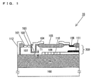
- FIG. 1 is a cross-sectional view of an exemplary main portion of a structure of the lateral semiconductor device 10 according to the first embodiment of the present invention.
- components necessary for describing the present embodiment are mainly indicated.
- the lateral semiconductor device 10 according to the first embodiment of the present invention is formed with the use of an SOI (Silicon on Insulator) substrate.
- the lateral semiconductor device 10 according to the first embodiment of the present invention includes: a single crystalline silicon support substrate 100; a buried oxide layer 200 layered over the single crystalline silicon support substrate 100; and a semiconductor layer 300.
- a surface portion of the semiconductor layer 300 may be covered with an interlayer insulating layer, and a potential source line or the like may be disposed on the interlayer insulating layer, which is not shown.
- the single crystalline silicon support substrate 100 is, for example, a layer containing a p-type impurity. Further, a resistivity of the single crystalline silicon support substrate 100 preferably indicates such a value as to maintain mechanical strength. For example, the resistivity preferably ranges from about 1 m ⁇ cm to about 100 m ⁇ cm.
- the single crystalline silicon substrate 100 is simply referred to as the support substrate 100 in the below description.
- the buried oxide layer 200 is preferably formed with the use of a material, such as silicon oxide, having a relatively low dielectric constant, and the thickness thereof in the layering direction (vertical direction) preferably ranges from about 3.0 ⁇ m to about 5.0 ⁇ m.
- the semiconductor layer 300 is a semiconductor layer that contains an n- type impurity in a relatively low concentration, and layer regions having different characteristics are partially formed in the semiconductor layer 300. Specifically, as shown in FIG. 1 , in the semiconductor layer 300, a contact body region (also referred to as a body P + diffusion layer) 101, an emitter region (also referred to as an emitter N + diffusion layer) 102, a main body region (also referred to as a body P diffusion layer) 107, a graded concentration diffusion layer 110, a buffer region (also referred to as a buffer N diffusion layer) 111, and the like are formed.
- a contact body region also referred to as a body P + diffusion layer
- an emitter region also referred to as an emitter N + diffusion layer
- main body region also referred to as a body P diffusion layer
- a graded concentration diffusion layer 110 also referred to as a buffer N diffusion layer
- a buffer region also referred to as a buffer N diffusion layer
- the main body region 107 is a layer region that contains a p-type impurity and is formed from the face of the semiconductor layer 300 to reach the back surface thereof.
- the emitter region 102 is a region that contains an n + type impurity in a higher concentration as compared to a main portion (n- type region; an active layer N - region 109) of the semiconductor layer 300.
- the emitter region 102 is formed in the main body region 107 on the face side of the semiconductor layer 300.
- the emitter region 102 is electrically connected to an emitter electrode that is one of main electrodes, which is not shown.
- the contact body region 101 is a region that contains a p + type impurity in a higher concentration as compared to the main body region 107.
- the contact body region 101 is formed in the main body region 107 on the face side of the semiconductor layer 300.
- the contact body region 101 has an ohmic connection to the emitter electrode, which is not shown.
- the buffer region 111 is a layer region containing an n-type impurity in a high concentration.
- a collector region (a collector P + diffusion layer) 106 is a region that contains a p + type impurity in a higher concentration as compared to the main body region 107.
- the collector region 106 is electrically connected to a collector electrode that is the other of the main electrodes, which is not shown.
- the graded concentration diffusion layer 110 is a layer region that is formed in the semiconductor layer 300 in a boundary of the buried oxide layer 200.
- the graded concentration diffusion layer 110 is a region that contains an n-type impurity, and is formed such that the concentration thereof is changed continuously or discontinuously over, for example, eight steps in the drift direction. More specifically, the concentration of the impurity in the graded concentration diffusion layer 110 increases from the emitter region 102 side toward the collector region 106 side.
- the contact body region 101, the emitter region 102, the collector region 106, the main body region 107, the graded concentration diffusion layer 110, and the buffer region 111 as described above, are formed by a conventionally well-known method such as an ion implantation or the like.
- a LOCOS (Local Oxidation of Silicon) oxide 105 is formed on or around the semiconductor layer 300 having been thus formed. Further, a gate oxide 103 and a poly gate electrode 104 are formed in the semiconductor layer 300 having been thus formed.
- the LOCOS oxide 105 is, for example, an oxide film formed on the face portion of the drift region 109.
- a material of the LOCOS oxide 105 is, for example, silicon oxide.
- the gate oxide 103 is an oxide layer that contacts with a portion of the drift region 109 and a portion of the main body region 107.
- the lateral semiconductor device 10 according to the first embodiment of the present invention has a characteristic that, as shown in FIG. 1 , a trench-type gate structure in which a trench does not reach the buried oxide layer 200 is formed in an interface between the main body region 107 and the drift region 109.
- a buried oxide layer is not formed under the main body region 107, namely, the carrier accumulation promoting BOX 201 (see FIG. 10 ) as formed in the lateral semiconductor device of Patent Literature 1 as described above is not formed. Therefore, a process of forming the carrier accumulation promoting BOX 201 is unnecessary, thereby simplifying a manufacturing method and reducing production cost (the manufacturing method will be described below in detail).
- the trench-type gate structure (hereinafter, simply referred to as a trench gate) is formed by the gate oxide 103 and the poly gate electrode 104 as shown in FIG. 1 .
- a thickness T1 that is, a thickness T1 of a gate portion active layer N- as shown in FIG. 1
- a route through which holes transfer from the drift region 109 to the main body region 107 is narrowed by the trench gate, and holes are accumulated, thereby reducing an on-resistance.
- a characteristic of a trade-off between a turn-off switching time (tf) and a collector-emitter saturation voltage (VCEsat) is also improved, without reducing a collector breakdown voltage (BVCEO) between collector and emitter, as compared to a conventional lateral semiconductor device (the lateral semiconductor device of Patent Literature 1 described above).
- a conventional lateral semiconductor device (specifically, the lateral semiconductor device of Patent Literature 1 as described above) and the lateral semiconductor device 10 according to the present embodiment are compared, and a flow of electron current in each of the lateral semiconductor devices will be described.
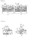
- FIG. 2 is a cross-sectional view of an exemplary main portion of the structure of the conventional lateral semiconductor device
- (b) of FIG. 2 is a cross-sectional view of an exemplary main portion of the structure of the lateral semiconductor device 10 according to the first embodiment.
- FIG. 10 is indicated again as (a) of FIG. 2
- FIG. 1 is indicated again as (b) of FIG. 2 .
- FIG. 3 are enlarged views of portions enclosed by broken lines in (a) and (b), respectively, of FIG. 2 .
- arrows are indicated in FIG. 3 .
- VGE gate-emitter voltage
- VT threshold voltage
- an n-type channel is formed in the interface between the gate oxide 103 and the main body region 107, to electrically connect between the emitter region 102 and the drift region 109, and electrons flow into the drift region 109.
- the electrons act as a base current of a pnp-type transistor that is formed by the main body region 107 (P-type), the drift region 109 and the buffer region 111 (n-type), and the collector region 106 (P-type), and the pnp transistor is turned on.
- the carrier accumulation promoting BOX 201 is formed to reduce an area in which the main body region 107 and the drift region 109a contact with each other, and holes can be restrained from transferring from the drift region 109a to the main body region 107 without preventing holes from transferring from the drift region 109b to the drift region 109a.
- an increased number of holes are accumulated in the drift region 109a, to reduce a resistance in the drift region 109a.
- a route through which holes transfer from the drift region 109 to the main body region 107 is narrowed (the thickness T1 of the gate portion active layer N - ) by the trench gate, and holes are accumulated, thereby reducing a resistance in the region.
- the width Lac is preferably in a range from about 1.0 ⁇ m to about 2.0 ⁇ m, and designing is performed in this range in general.
- a flow of electron current is as indicated by dashed arrows in (b) of FIG. 3 , and even when a width Lac is reduced, neither a resistance Rac1 nor a resistance Rac2 is increased.
- the width Lac can be in a range from about 0.2 ⁇ m to about 0.5 ⁇ m.
- width Lch width Lch1 + width Lch2 in (b) of FIG. 3 .
- width Lch1 width Lch1 + width Lch2 in (b) of FIG. 3 .
- the thickness T1 of the drift region 109 can be reduced (the thickness T1 of the gate portion active layer N- in FIG. 1 and (b) of FIG. 2 ), and accumulation of holes in the vicinity of the thin portion is increased as compared to in the conventional lateral semiconductor devices. Therefore, a resistance can be greatly reduced in this region.
- a cell pitch can be reduced (width 113a > width 113b) as compared to in the conventional lateral semiconductor devices, a characteristic of a trade-off between a turn-off switching time (tf) and a collector-emitter saturation voltage (VCEsat) can be improved without reducing a collector breakdown voltage (BVCEO).
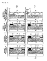
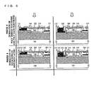
- FIG. 4 to FIG. 6 illustrate an exemplary manufacturing process for manufacturing the lateral semiconductor device 10 according to the first embodiment of the present invention.
- the lateral semiconductor device according to the first embodiment of the present invention is represented as the lateral semiconductor device 10 by using reference character, and what is simply referred to as a lateral semiconductor device represents the lateral semiconductor device according to the first embodiment of the present invention and the conventional lateral semiconductor device.
- the manufacturing method for manufacturing the lateral semiconductor device 10 according to the first embodiment of the present invention has a characteristic that, as described above, a process of forming a buried oxide layer disposed under the main body region 107, that is, the carrier accumulation promoting BOX 201 (see FIG. 10 ) as is formed in the conventional lateral semiconductor device, is unnecessary, and the trench-type gate structure in which the trench does not reach the buried oxide layer 200 is formed in the interface between the main body region 107 and the drift region 109.
- the manufacturing method for manufacturing the lateral semiconductor device 10 according to the first embodiment of the invention will be described particularly according to the characteristic described above.
- the support substrate 100 contains, for example, a p-type impurity. Further, a resistivity of the support substrate 100 preferably indicates such a value as to maintain mechanical strength. For example, the resistivity preferably ranges from about 1 m ⁇ cm to about 100 m ⁇ cm.
- the buried oxide layer 200 is preferably formed with the use of a material, such as silicon oxide, having a relatively low dielectric constant.
- the thickness thereof in the layering direction ranges from about 3.0 ⁇ m to about 5.0 ⁇ m in the case of a withstand voltage being about 700V, and ranges from about 10 ⁇ m to about 15 ⁇ m in the case of a withstand voltage being about 2000V.
- a thickness T2 of the drift region 109 is about 2.0 ⁇ m, and a concentration of an impurity (phosphorus) to be injected is about 1e15cm -3 .
- process 2 in FIG. 4 is a process of forming the carrier accumulation promoting BOX 201 (see FIG. 10 ).
- Process 2 in FIG. 4 will be specifically described.
- a SIMOX (Separation by IMplanted Oxygen) method is applied, a resist is firstly applied to the surface of the drift region 109, and ions of oxygen (O 2 ) are implanted with a high energy (an oxygen ion implantation process of process 2 in FIG. 4 ). Thereafter, for example, heat treatment at about 1100°C to about 1300°C is performed by using a thermal oxidation device, to obtain the carrier accumulation promoting BOX 201 (a heat treatment process of process 2 in FIG. 4 ).
- a depth T3 of the LOCOS oxide 105 from the surface portion of the drift region 109 to an inner portion of the drift region 109 preferably ranges from about 0.3 ⁇ m to about 0.5 ⁇ m.
- a trench TL1 for a gate electrode is formed from the surface of the drift region 109 toward the buried oxide layer 200 so as not to reach the buried oxide layer 200, and a trench TL2 for a device-isolating electrode is formed so as to pass through the LOCOS oxide 105 and reach the buried oxide layer 200.
- process 4 will be specifically described. More specifically, in process 4 in FIG. 5 , process 4-1 and process 4-2 are performed as described below.
- an Si/SiO 2 interface in a region in which the LOCOS oxide 105 is formed is located so as to be deeper than the surface of an active region (the drift region 109) by the depth T3.
- an etching process is performed on the LOCOS oxide 105. More specifically, the LOCOS oxide 105 is etched such that a depth from the surface of the drift region 109 is the depth T3. In other words, as indicated in process 4 in FIG. 5 , the LOCOS oxide 105 is etched by a depth T4 from the surface of the LOCOS oxide 105 toward the oxide layer 200. This process is referred to as process 4-1, which is not indicated in the drawings.
- a resist is applied to the surface of the drift region 109, and exposure to light and development are performed on the resist at predetermined pitches, to form openings on the resist, and the trench TL1 and the trench TL2 are then formed toward the buried oxide layer 200 by dry etching or the like.
- the forming of the trench TL1 and the forming of the trench TL2 are simultaneously started, and an engraving speed (an engraving rate, an etching rate) are the same therebetween.
- the trench TL1 is formed by, for example, etching from the surface of the drift region 109 toward the buried oxide layer 200 being performed
- the trench TL2 is formed by, for example, etching from a position (the portion obtained by the etching of process 4-1) that is deeper than the surface of the drift region 109 by the depth T3, toward the buried oxide layer 200, being performed.
- process 4-2 which is not indicated in the drawings.
- the LOCOS oxide 105 is etched, and thereafter the etching for forming the trench TL1 and the etching for forming the trench TL2 are simultaneously started so as to be performed at the same rate.
- the forming of the trench TL1 and the forming of the trench TL2 are stopped.
- the trench TL1 is formed so as not to reach the buried oxide layer 200 (so as to obtain the thickness T1 of the gate portion active layer N - ).
- the trench TL1 and the trench TL2 can be simultaneously formed.
- Process 4-1 described above corresponds to an example of an etching process as recited in claim 6.
- Process 4-2 described above corresponds to an example of a trench forming process as recited in claim 6.
- various diffusion layers are formed by a typical ion implantation method.
- a concentration of an impurity in the graded concentration diffusion layer 110 is distributed into, for example, eight steps of concentrations.
- the gate oxide 103 is formed specifically by a thermal oxidation process or the like, for example. Further, in process 6, not only side walls of the trench TL1 for the gate electrode but also side walls of the trench TL2 for the device-isolating electrode are oxidized. The thickness of an oxide layer of the side walls of the trench TL2 for the device-isolating electrode is equal to the thickness of an oxide layer of the side walls of the trench TL1 for the gate electrode. Therefore, plural trenches could be enough to meet a demand for high voltage isolation. However, in the lateral semiconductor device 10, the trench TL2 for the device-isolating electrode is formed in the main body region 107 that keeps low potential. Therefore, one trench is sufficient.
- Si single crystals that have a good filling characteristic of filling the trenches TL1 and TL2 by a CVD (Chemical Vapor Deposition) method or the like are deposited and grown in each of the trenches.
- the trenches are simultaneously filled with Si single crystals.
- the process is advanced to process 8 in FIG. 6 .
- Patterning is performed on the Si single crystals deposited in process 7, and etching is then performed thereon.
- the poly gate electrode 104 and a poly trench electrode 112 are formed.
- the contact body region 101, the emitter region (emitter N + diffusion layer) 102, and the collector region (collector P + diffusion layer) 106 are formed by ion implantation.
- the process of forming the carrier accumulation promoting BOX 201 as is performed for manufacturing the conventional lateral semiconductor devices is unnecessary, and therefore the lateral semiconductor device 10 can be manufactured in a simplified method, and production cost can be reduced.
- the buried oxide layer 200 disposed under the P-type body layer 107 among the P-type body layer 107 and the N-type drift layers 109a and 109b has a thickness (the carrier accumulation promoting BOX 201) that is greater than a remaining region of the buried oxide layer 200 disposed under the N-type drift layers 109a and 109b.
- the carrier accumulation promoting BOX 201 the carrier accumulation promoting BOX 201 that is greater than a remaining region of the buried oxide layer 200 disposed under the N-type drift layers 109a and 109b.
- a cost for a process of forming the trench is lower than a cost for a process of forming the carrier accumulation promoting BOX 201.
- a process of forming the carrier accumulation promoting BOX 201 need not be performed, and production cost can be thus reduced, and an on-resistance can be reduced in a simplified method as compared to the conventional lateral semiconductor devices.
- FIG. 7 is a cross-sectional view of an exemplary main portion of a structure of the lateral semiconductor device 20 according to the second embodiment.
- the lateral semiconductor device 20 according to the second embodiment is different from the lateral semiconductor device 10 according to the first embodiment as described above in that an emitter region (also referred to as an emitter N + diffusion layer) 102 is formed toward the buried oxide layer 200 so as to be deeper in the lateral semiconductor device 20 than in the lateral semiconductor device 10. More specifically, a distance from the surface of the buried oxide layer 200 to the emitter region 102 is less than a distance (the thickness T1) from the bottom of the trench TL1 to the buried oxide layer 200.
- an emitter region also referred to as an emitter N + diffusion layer
- a channel which has only the Lch2 shown in FIG. 3 can be formed, and a channel length can be shortened as compared to that in the lateral semiconductor device 10 according to the first embodiment as described above.
- electron currents flowing into the drift region 109 can be increased as compared to in the lateral semiconductor device 10 according to the first embodiment, and a trade-off characteristic can be improved as compared to in the lateral semiconductor device 10 according to the first embodiment as well as the conventional lateral semiconductor devices (the details will be described below).
- the emitter region 102 as described above can be obtained by, for example, patterning for the emitter region 102 in process 9 in the manufacturing method for manufacturing the lateral semiconductor device 10 according to the first embodiment as shown in FIG. 6 , being changed (so as to cross the emitter region 102 and the trench TL1).
- FIG. 8 is a cross-sectional view of an exemplary main portion of a structure of the lateral semiconductor device 30 according to the third embodiment.
- the lateral semiconductor device 30 according to the third embodiment is different from the lateral semiconductor device 10 according to the first embodiment as described above in that the lateral semiconductor device 30 includes a carrier accumulation layer region (N-layer for storing carriers) 114 in addition to the components of the lateral semiconductor device 10 according to the first embodiment.
- N-layer for storing carriers carrier accumulation layer region
- ion implantation for forming the carrier accumulation layer region 114 may be performed in process 5 in the manufacturing method for manufacturing the lateral semiconductor device 10 according to the first embodiment as shown in FIG. 5 .
- a concentration of an impurity in the carrier accumulation layer region 114 is preferably high, and the width of the carrier accumulation layer region 114 is preferably great.
- the width is preferably about 1.0 ⁇ m, and a concentration of an impurity therein preferably ranges from about 1 cm -3 to about 3e17 cm -3 .
- FIG. 9 illustrates collector-emitter saturation voltage (VCEsat) - turn-off switching time (tf) characteristics in the lateral semiconductor devices according to the respective embodiments and a conventional lateral semiconductor device.
- VCEsat collector-emitter saturation voltage
- tf turn-off switching time
- the horizontal axis represents VCEsat in arbitrary units (A.U)
- the vertical axis represents tf in arbitrary units.
- Trade-off characteristics of the lateral semiconductor devices according to the respective embodiments are indicated by solid lines, and a trade-off characteristic of the conventional lateral semiconductor device is indicated by a broken line.
- the characteristic of the trade-off between tf and VCEsat is greatly improved in the lateral semiconductor device 10 according to the first embodiment as compared to the conventional lateral semiconductor device. Further, it can be found that the characteristic of the trade-off between tf and VCEsat is improved in the lateral semiconductor device 20 according to the second embodiment as compared to the lateral semiconductor device 10 according to the first embodiment. Moreover, it can be found that the characteristic of the trade-off between tf and VCEsat is improved in the lateral semiconductor device 30 according to the third embodiment as compared to the lateral semiconductor device 20 according to the second embodiment.
- the lateral semiconductor device and the manufacturing method for the same according to the present invention can be used as, for example, a lateral insulated gate bipolar transistor that can increase reduction of an on-resistance in a simplified method.
Landscapes
- Thin Film Transistor (AREA)
- Chemical & Material Sciences (AREA)
- Chemical Kinetics & Catalysis (AREA)
- General Chemical & Material Sciences (AREA)
- Electrodes Of Semiconductors (AREA)
- Bipolar Transistors (AREA)
Abstract
Description
- The present invention relates to semiconductor devices, and more particularly to lateral IGBTs (Insulated Gate Bipolar Transistors) and a manufacturing method for the same.
- To date, integrated circuits (also referred to as ICs) each of which has semiconductor devices such as a diode and a transistor, and driving control circuits for the semiconductor devices integrated on one silicon substrate, have been developed. In particular, a lateral insulated gate bipolar transistor (LIGBT, hereinafter, simply referred to as a lateral semiconductor device) is a power transistor that includes a MOS input structure, and a bipolar output structure, and is a semiconductor that has an advantage that high power driving can be derived from less power with its high voltage and current semiconductor properties.
- The lateral semiconductor device has a characteristic that conductivity modulation is enhanced in a drift region in an on-state, thereby obtaining a low on-voltage (on-resistance). For example, a technique disclosed in
Patent Literature 1 represents an example of the lateral semiconductor device. - Patent Literature 1: Japanese Laid-Open Patent Publication No.
2010-251627 - As shown in
FIG. 10 , in the lateral semiconductor device disclosed inPatent Literature 1, a buriedoxide layer 200 disposed under a P-type body layer 107 among the P-type body layer 107 and N-type drift layers oxide layer 200 disposed under the N-type drift layers drift layer region 109a to the P-type body layer 107 to reduce an on-resistance, as compared to the N-typedrift layer region 109b. - In the description herein, the buried
oxide layer 200 disposed under the P-type body layer 107 portion is particularly referred to as a carrieraccumulation promoting BOX 201. - Although an on-resistance is reduced in the lateral semiconductor device disclosed in
Patent Literature 1 in the method as described above, a problem arises that production cost is increased. Namely, as shown inFIG. 10 , the carrieraccumulation promoting BOX 201 is formed to partially increase a thickness of the buried oxide layer, thereby realizing reduction of an on-resistance. - However, in order to manufacture the lateral semiconductor device disclosed in
Patent Literature 1, a process of forming the carrieraccumulation promoting BOX 201 is performed in addition to processes for manufacturing a lateral semiconductor device that does not have the carrieraccumulation promoting BOX 201. - The present invention is made in view of the aforementioned situation, and an object of the present invention is to make available a lateral semiconductor device with a lower on-resistance structure than taught in
Patent Literature 1 while simplifying the manufacturing process, and a manufacturing method for the same. - A first aspect of the present invention is directed to a lateral semiconductor device having an SOI (Silicon on Insulator) substrate. The lateral semiconductor device includes a semiconductor layer including a body region (107) on a buried oxide layer (200), and a drift region (109) that contacts with a side surface of the body region (107). Further, the lateral semiconductor device has a first trench that is recessed, toward the buried oxide layer (200), in an interface between the body region (107) and the drift region (109) so as not to reach the buried oxide layer (200).
- In a second aspect of the present invention based on the first aspect, a value of a distance from a bottom of the first trench to the buried oxide layer (200) is less than a value of a thickness of the drift region (109) represented as a value of a distance from a surface of the buried oxide layer (200) to a surface of the drift region (109).
- In a third aspect of the present invention based on the second aspect, an emitter region (102) that does not reach the buried oxide layer (200) is formed in the body region (107) so as to contact with a side surface of the first trench. Further, a distance from the surface of the buried oxide layer (200) to the emitter region (102) is less than a distance from the bottom of the first trench to the buried oxide layer (200).
- In a fourth aspect of the present invention based on the second aspect, a carrier accumulation layer region (114) is formed in the drift region (109) so as to contact with the bottom of the first trench and the side surface of the body region (107). Further, a concentration of an impurity in the carrier accumulation layer region (114) is higher than a concentration of an impurity in the drift region (109).
- In a fifth aspect of the present invention based on the first aspect, a second trench that passes through a LOCOS oxide (105) so as to reach the buried oxide layer (200) is further provided, and the LOCOS oxide (105) projects from a surface of the semiconductor layer by a predetermined thickness and is embedded in the semiconductor layer by a predetermined thickness. The first trench is recessed in the semiconductor layer so as to extend from a portion in which the LOCOS oxide (105) is not formed.
- A sixth aspect of the present invention is directed to a manufacturing method for manufacturing a lateral semiconductor device having an SOI (Silicon on Insulator) substrate. The lateral semiconductor device includes a semiconductor layer that includes a buried oxide layer (200) and a drift region (109). The manufacturing method includes an etching process of etching, by a predetermined depth, a LOCOS oxide (105) that projects from a surface of the semiconductor layer by a predetermined thickness and is embedded in the semiconductor layer by a predetermined thickness, and a trench forming process of simultaneously forming a first trench extending from the drift region (109) toward the buried oxide layer (200), and a second trench extending from a portion obtained by the etching in the etching process toward the buried oxide layer (200), at a same etching rate, and stopping forming the first trench and the second trench at a time when the second trench reaches the buried oxide layer (200).
- According to the first aspect, the lateral semiconductor device with a lower on-resistance structure than conventional lateral semiconductor devices while simplifying the manufacturing process, can be provided. Namely, in the conventional lateral semiconductor devices, a thickness of a buried oxide layer disposed under a P-type body layer is made greater than a thickness of a remaining region of the buried
oxide layer 200 disposed under an N-type drift layer (carrier accumulation promoting BOX). - Thus, fewer holes drift through from the N-type drift layer region to the P-type body layer to reduce an on-resistance. On the other hand, in the lateral semiconductor device according to the present invention, a route through which holes transfer from the
drift region 109 to themain body region 107 is narrowed by the trench gate, and holes are accumulated, thereby reducing an on-resistance. Namely, the lateral semiconductor device according to the present invention need not include the carrier accumulation promoting BOX. Therefore, since a cost for a process of forming the trench is lower than a cost for a process of forming the carrier accumulation promoting BOX, production cost can be reduced. - Further, in the lateral semiconductor device according to the present invention, a trench-type gate structure in which a trench does not reach the buried
oxide layer 200 is formed in an interface between themain body region 107 anddrift region 109. Therefore, the thickness of thedrift region 109 can be extremely reduced, and storing of holes is enhanced near a region in which the thickness is reduced, as compared to in the conventional lateral semiconductor devices. Therefore, a resistance in the region can be also reduced greatly. - According to the second aspect, the value of the distance from the bottom of the trench to the buried
oxide layer 200 is less than the value of the thickness of thedrift region 109 represented as the value of the distance from the surface of the buriedoxide layer 200 to the surface of thedrift region 109, thereby reducing holes transferred to themain body region 107. Thus, electric charge is stored to enable reduction of a resistance. - According to the third aspect, electron current flowing into the
drift region 109 can be increased, thereby enabling improvement of a trade-off characteristic. - According to the fourth aspect, the carrier
accumulation layer region 114 in which a concentration of an impurity is high is formed in thedrift region 109. Therefore, holes are less likely to transfer from thedrift region 109 to themain body region 107, and carrier storing effect is enhanced, to enable improvement of a trade-off characteristic. - According to the fifth aspect, the second trench passes through the
LOCOS oxide 105 so as to reach the buried oxide layer, and the first trench is recessed in a region in which theLOCOS oxide 105 is not formed. Therefore, for example, a process cost for forming a trench for a gate electrode and a trench for a device-isolating electrode can be reduced. Namely, if, after theLOCOS oxide 105 is etched, etching for forming the first trench and etching for forming the second trench are simultaneously started so as to be performed at the same rate, when the second trench reaches the buried oxide layer, the first trench is formed. Thus, each of the trenches can be simultaneously formed in one process. - According to the sixth aspect, the same effect as that of the first aspect can be obtained, and further, for example, a trench for a gate electrode and a trench for a device-isolating electrode can be formed in one process, thereby reducing a process cost.
-
- [
FIG. 1] FIG. 1 is a cross-sectional view of an exemplary main portion of a structure of alateral semiconductor device 10 according to a first embodiment. - [
FIG. 2] FIG. 2 is cross-sectional views of an exemplary main portion of the structure of thelateral semiconductor device 10, and an exemplary main portion of a structure of a conventional lateral semiconductor device. - [
FIG. 3] FIG. 3 is enlarged views of portions, inFIG. 2 , enclosed by broken lines. - [
FIG. 4] FIG. 4 illustrates an exemplary manufacturing process (process 1 to process 3) for manufacturing thelateral semiconductor device 10 according to the first embodiment. - [
FIG. 5] FIG. 5 illustrates an exemplary manufacturing process (process 4 to process 7) for manufacturing thelateral semiconductor device 10 according to the first embodiment. - [
FIG. 6] FIG. 6 illustrates an exemplary manufacturing process (process 8 to process 9) for manufacturing thelateral semiconductor device 10 according to the first embodiment. - [
FIG. 7] FIG. 7 is a cross-sectional view of an exemplary main portion of a structure of alateral semiconductor device 20 according to a second embodiment. - [
FIG. 8] FIG. 8 is a cross-sectional view of an exemplary main portion of a structure of alateral semiconductor device 30 according to a third embodiment. - [
FIG. 9] FIG. 9 illustrates collector-emitter saturation voltage (VCEsat) - turn-off switching time (tf) characteristics in the lateral semiconductor devices according to the respective embodiments and a conventional lateral semiconductor device. - [
FIG. 10] FIG. 10 is a cross-sectional view of an exemplary main portion of a structure of a conventional lateral semiconductor device. - Hereinafter, a lateral IGBT (Insulated Gate Bipolar Transistor, hereinafter, simply referred to as a lateral semiconductor device 10) according to a first embodiment of the present invention will be described with reference to the drawings.
- Firstly, a structure of the
lateral semiconductor device 10 according to the first embodiment of the present invention will be described with reference to the drawings. -
FIG. 1 is a cross-sectional view of an exemplary main portion of a structure of thelateral semiconductor device 10 according to the first embodiment of the present invention. InFIG. 1 , components necessary for describing the present embodiment are mainly indicated. - As shown in
FIG. 1 , thelateral semiconductor device 10 according to the first embodiment of the present invention is formed with the use of an SOI (Silicon on Insulator) substrate. Specifically, thelateral semiconductor device 10 according to the first embodiment of the present invention includes: a single crystallinesilicon support substrate 100; a buriedoxide layer 200 layered over the single crystallinesilicon support substrate 100; and asemiconductor layer 300. A surface portion of thesemiconductor layer 300 may be covered with an interlayer insulating layer, and a potential source line or the like may be disposed on the interlayer insulating layer, which is not shown. - The single crystalline
silicon support substrate 100 is, for example, a layer containing a p-type impurity. Further, a resistivity of the single crystallinesilicon support substrate 100 preferably indicates such a value as to maintain mechanical strength. For example, the resistivity preferably ranges from about 1 mΩ·cm to about 100 mΩ·cm. The singlecrystalline silicon substrate 100 is simply referred to as thesupport substrate 100 in the below description. - The buried
oxide layer 200 is preferably formed with the use of a material, such as silicon oxide, having a relatively low dielectric constant, and the thickness thereof in the layering direction (vertical direction) preferably ranges from about 3.0 µm to about 5.0 µm. - The
semiconductor layer 300 is a semiconductor layer that contains an n- type impurity in a relatively low concentration, and layer regions having different characteristics are partially formed in thesemiconductor layer 300. Specifically, as shown inFIG. 1 , in thesemiconductor layer 300, a contact body region (also referred to as a body P+ diffusion layer) 101, an emitter region (also referred to as an emitter N+ diffusion layer) 102, a main body region (also referred to as a body P diffusion layer) 107, a gradedconcentration diffusion layer 110, a buffer region (also referred to as a buffer N diffusion layer) 111, and the like are formed. - The
main body region 107 is a layer region that contains a p-type impurity and is formed from the face of thesemiconductor layer 300 to reach the back surface thereof. - The
emitter region 102 is a region that contains an n+ type impurity in a higher concentration as compared to a main portion (n- type region; an active layer N- region 109) of thesemiconductor layer 300. Theemitter region 102 is formed in themain body region 107 on the face side of thesemiconductor layer 300. Theemitter region 102 is electrically connected to an emitter electrode that is one of main electrodes, which is not shown. - The
contact body region 101 is a region that contains a p+ type impurity in a higher concentration as compared to themain body region 107. Thecontact body region 101 is formed in themain body region 107 on the face side of thesemiconductor layer 300. Thecontact body region 101 has an ohmic connection to the emitter electrode, which is not shown. - The
buffer region 111 is a layer region containing an n-type impurity in a high concentration. - A collector region (a collector P+ diffusion layer) 106 is a region that contains a p+ type impurity in a higher concentration as compared to the
main body region 107. Thecollector region 106 is electrically connected to a collector electrode that is the other of the main electrodes, which is not shown. - The graded
concentration diffusion layer 110 is a layer region that is formed in thesemiconductor layer 300 in a boundary of the buriedoxide layer 200. The gradedconcentration diffusion layer 110 is a region that contains an n-type impurity, and is formed such that the concentration thereof is changed continuously or discontinuously over, for example, eight steps in the drift direction. More specifically, the concentration of the impurity in the gradedconcentration diffusion layer 110 increases from theemitter region 102 side toward thecollector region 106 side. - The
contact body region 101, theemitter region 102, thecollector region 106, themain body region 107, the gradedconcentration diffusion layer 110, and thebuffer region 111 as described above, are formed by a conventionally well-known method such as an ion implantation or the like. - A LOCOS (Local Oxidation of Silicon)
oxide 105 is formed on or around thesemiconductor layer 300 having been thus formed. Further, agate oxide 103 and apoly gate electrode 104 are formed in thesemiconductor layer 300 having been thus formed. - The
LOCOS oxide 105 is, for example, an oxide film formed on the face portion of thedrift region 109. A material of theLOCOS oxide 105 is, for example, silicon oxide. - The
gate oxide 103 is an oxide layer that contacts with a portion of thedrift region 109 and a portion of themain body region 107. - The
lateral semiconductor device 10 according to the first embodiment of the present invention has a characteristic that, as shown inFIG. 1 , a trench-type gate structure in which a trench does not reach the buriedoxide layer 200 is formed in an interface between themain body region 107 and thedrift region 109. - In other words, in the
lateral semiconductor device 10 according to the present embodiment, as shown inFIG. 1 , a buried oxide layer is not formed under themain body region 107, namely, the carrier accumulation promoting BOX 201 (seeFIG. 10 ) as formed in the lateral semiconductor device ofPatent Literature 1 as described above is not formed. Therefore, a process of forming the carrieraccumulation promoting BOX 201 is unnecessary, thereby simplifying a manufacturing method and reducing production cost (the manufacturing method will be described below in detail). - Specifically, the trench-type gate structure (hereinafter, simply referred to as a trench gate) is formed by the
gate oxide 103 and thepoly gate electrode 104 as shown inFIG. 1 . Thus, a thickness T1 (that is, a thickness T1 of a gate portion active layer N- as shown inFIG. 1 ) of thedrift region 109 can be reduced. In other words, a route through which holes transfer from thedrift region 109 to themain body region 107 is narrowed by the trench gate, and holes are accumulated, thereby reducing an on-resistance. - A characteristic of a trade-off between a turn-off switching time (tf) and a collector-emitter saturation voltage (VCEsat) is also improved, without reducing a collector breakdown voltage (BVCEO) between collector and emitter, as compared to a conventional lateral semiconductor device (the lateral semiconductor device of
Patent Literature 1 described above). - With reference to
FIG. 2 and FIG. 3 , a conventional lateral semiconductor device (specifically, the lateral semiconductor device ofPatent Literature 1 as described above) and thelateral semiconductor device 10 according to the present embodiment are compared, and a flow of electron current in each of the lateral semiconductor devices will be described. - (a) of
FIG. 2 is a cross-sectional view of an exemplary main portion of the structure of the conventional lateral semiconductor device, and (b) ofFIG. 2 is a cross-sectional view of an exemplary main portion of the structure of thelateral semiconductor device 10 according to the first embodiment. For the description,FIG. 10 is indicated again as (a) ofFIG. 2 , andFIG. 1 is indicated again as (b) ofFIG. 2 . - Further, (a) and (b) of
FIG. 3 are enlarged views of portions enclosed by broken lines in (a) and (b), respectively, ofFIG. 2 . For the below description, arrows are indicated inFIG. 3 . - In general, when a gate-emitter voltage (VGE) is higher than a threshold voltage (VT), an n-type channel is formed in the interface between the
gate oxide 103 and themain body region 107, to electrically connect between theemitter region 102 and thedrift region 109, and electrons flow into thedrift region 109. The electrons act as a base current of a pnp-type transistor that is formed by the main body region 107 (P-type), thedrift region 109 and the buffer region 111 (n-type), and the collector region 106 (P-type), and the pnp transistor is turned on. - Since electrons are supplied from the
emitter region 102 and holes are injected from thecollector region 106, excessive electrons and holes are accumulated in the drift region 109 (a phenomenon called conductivity modulation). - In the conventional lateral semiconductor device, as shown in (a) of
FIG. 2 , particularly in (a) ofFIG. 3 , the carrieraccumulation promoting BOX 201 is formed to reduce an area in which themain body region 107 and thedrift region 109a contact with each other, and holes can be restrained from transferring from thedrift region 109a to themain body region 107 without preventing holes from transferring from thedrift region 109b to thedrift region 109a. As a result, an increased number of holes are accumulated in thedrift region 109a, to reduce a resistance in thedrift region 109a. - On the other hand, in the
lateral semiconductor device 10 according to the first embodiment of the present invention, as shown in (b) ofFIG. 2 , particularly in (b) ofFIG. 3 , a route through which holes transfer from thedrift region 109 to themain body region 107 is narrowed (the thickness T1 of the gate portion active layer N-) by the trench gate, and holes are accumulated, thereby reducing a resistance in the region. - With reference to (a) and (b) of
FIG. 3 , a flow of electron current in each of the conventional lateral semiconductor device (the lateral semiconductor device ofPatent Literature 1 as described above) and thelateral semiconductor device 10 according to the present embodiment, will be more specifically described. - Firstly, a flow of electron current in a region indicated by 113a in (a) of
FIG. 2 will be described in the case of, for example, the conventional lateral semiconductor device shown in (a) ofFIG. 2 . - In the conventional lateral semiconductor device, when a positive electric potential is applied to the
poly gate electrode 104, a channel is formed just below thegate oxide 103, and electron current flows from thedrift layer region 109a to thedrift layer region 109b as indicated by dashed arrows in (a) ofFIG. 3 . - At this time, when a width Lac is excessively small, a resistance Rac is increased. Therefore, in general, the width Lac is preferably in a range from about 1.0 µm to about 2.0 µm, and designing is performed in this range in general. In order to restrain a saturation current and improve resistance to short-circuiting, a width Lch is preferably in a range from about 1.5 µm to about 2.0 µm, and designing is performed in this range in general, and the width Lch cannot be extremely reduced. Therefore, the
width 113a is approximately in a range from 2.5 µm to 4.0 µm (width 113a = width Lch + width Lac). - Next, a flow of electron current in a region indicated by 113b in (a) of
FIG. 3 will be described for thelateral semiconductor device 10 according to the first embodiment of the present invention as shown in (b) ofFIG. 3 . - In the
lateral semiconductor device 10 according to the first embodiment of the present invention, a flow of electron current is as indicated by dashed arrows in (b) ofFIG. 3 , and even when a width Lac is reduced, neither a resistance Rac1 nor a resistance Rac2 is increased. Thus, the width Lac can be in a range from about 0.2 µm to about 0.5 µm. - The width Lch as indicated in (a) of
FIG. 3 can be represented as width Lch = width Lch1 + width Lch2 in (b) ofFIG. 3 . Further, when the width Lch1 is about 1.0 µm, the width Lch2 is in a range from about 0.5 µm to about 1.0 µm. Therefore, thewidth 113b is approximately in a range from 0.7 µm to 1.5 µm (width 113b = width Lch2 + width Lac). - As described above, in the
lateral semiconductor device 10 according to the first embodiment of the present invention, since the trench-type gate structure in which the trench does not reach the buriedoxide layer 200 is formed in the interface between themain body region 107 and thedrift region 109, the thickness T1 of thedrift region 109 can be reduced (the thickness T1 of the gate portion active layer N- inFIG. 1 and (b) ofFIG. 2 ), and accumulation of holes in the vicinity of the thin portion is increased as compared to in the conventional lateral semiconductor devices. Therefore, a resistance can be greatly reduced in this region. - Further, as described above, since a cell pitch can be reduced (
width 113a >width 113b) as compared to in the conventional lateral semiconductor devices, a characteristic of a trade-off between a turn-off switching time (tf) and a collector-emitter saturation voltage (VCEsat) can be improved without reducing a collector breakdown voltage (BVCEO). - Comparison in trade-off characteristic among the
lateral semiconductor device 10 according to the first embodiment of the present invention, lateral semiconductor devices according to second and third embodiments as described below, and the conventional lateral semiconductor device, will be described below. - Next, a manufacturing method for manufacturing the
lateral semiconductor device 10 according to the first embodiment of the present invention will be described with reference to the drawings.FIG. 4 to FIG. 6 illustrate an exemplary manufacturing process for manufacturing thelateral semiconductor device 10 according to the first embodiment of the present invention. - In the following description, with reference to
FIG. 4 to FIG. 6 , an exemplary manufacturing process for manufacturing thelateral semiconductor device 10 according to the first embodiment of the present invention will be described together with an exemplary manufacturing process for manufacturing the conventional lateral semiconductor device (specifically, the lateral semiconductor device ofPatent Literature 1 described above). - Further, in the following description, the lateral semiconductor device according to the first embodiment of the present invention is represented as the
lateral semiconductor device 10 by using reference character, and what is simply referred to as a lateral semiconductor device represents the lateral semiconductor device according to the first embodiment of the present invention and the conventional lateral semiconductor device. - The manufacturing method for manufacturing the
lateral semiconductor device 10 according to the first embodiment of the present invention has a characteristic that, as described above, a process of forming a buried oxide layer disposed under themain body region 107, that is, the carrier accumulation promoting BOX 201 (seeFIG. 10 ) as is formed in the conventional lateral semiconductor device, is unnecessary, and the trench-type gate structure in which the trench does not reach the buriedoxide layer 200 is formed in the interface between themain body region 107 and thedrift region 109. Hereinafter, the manufacturing method for manufacturing thelateral semiconductor device 10 according to the first embodiment of the invention will be described particularly according to the characteristic described above. - For the lateral semiconductor device, as indicated in
process 1 inFIG. 4 , firstly, an SOI (Silicon On Insulator) wafer is used. Thesupport substrate 100 contains, for example, a p-type impurity. Further, a resistivity of thesupport substrate 100 preferably indicates such a value as to maintain mechanical strength. For example, the resistivity preferably ranges from about 1 mΩ·cm to about 100 mΩ·cm. The buriedoxide layer 200 is preferably formed with the use of a material, such as silicon oxide, having a relatively low dielectric constant. The thickness thereof in the layering direction (vertical direction) ranges from about 3.0 µm to about 5.0 µm in the case of a withstand voltage being about 700V, and ranges from about 10 µm to about 15 µm in the case of a withstand voltage being about 2000V. A thickness T2 of thedrift region 109 is about 2.0 µm, and a concentration of an impurity (phosphorus) to be injected is about 1e15cm-3. - Next,
process 2 inFIG. 4 will be described. However, as described above, in the manufacturing method for manufacturing thelateral semiconductor device 10,process 2 need not be performed. Namely, to be specific,process 2 is a process of forming the carrier accumulation promoting BOX 201 (seeFIG. 10 ). -
Process 2 inFIG. 4 will be specifically described. For example, in a case where a SIMOX (Separation by IMplanted Oxygen) method is applied, a resist is firstly applied to the surface of thedrift region 109, and ions of oxygen (O2) are implanted with a high energy (an oxygen ion implantation process ofprocess 2 inFIG. 4 ). Thereafter, for example, heat treatment at about 1100°C to about 1300°C is performed by using a thermal oxidation device, to obtain the carrier accumulation promoting BOX 201 (a heat treatment process ofprocess 2 inFIG. 4 ). - Next, the process is advanced to
process 3, and, for example, a layer of silicon oxide, that is, theLOCOS oxide 105 is formed on the surface portion of thedrift region 109. A depth T3 of theLOCOS oxide 105 from the surface portion of thedrift region 109 to an inner portion of thedrift region 109 preferably ranges from about 0.3 µm to about 0.5 µm. - The process is advanced to
process 4 inFIG. 5 . For thelateral semiconductor device 10, a trench TL1 for a gate electrode is formed from the surface of thedrift region 109 toward the buriedoxide layer 200 so as not to reach the buriedoxide layer 200, and a trench TL2 for a device-isolating electrode is formed so as to pass through theLOCOS oxide 105 and reach the buriedoxide layer 200. - The
process 4 will be specifically described. More specifically, inprocess 4 inFIG. 5 , process 4-1 and process 4-2 are performed as described below. - As shown in
FIG. 5 , an Si/SiO2 interface in a region in which theLOCOS oxide 105 is formed is located so as to be deeper than the surface of an active region (the drift region 109) by the depth T3. - Firstly, an etching process is performed on the
LOCOS oxide 105. More specifically, theLOCOS oxide 105 is etched such that a depth from the surface of thedrift region 109 is the depth T3. In other words, as indicated inprocess 4 inFIG. 5 , theLOCOS oxide 105 is etched by a depth T4 from the surface of theLOCOS oxide 105 toward theoxide layer 200. This process is referred to as process 4-1, which is not indicated in the drawings. - A resist is applied to the surface of the
drift region 109, and exposure to light and development are performed on the resist at predetermined pitches, to form openings on the resist, and the trench TL1 and the trench TL2 are then formed toward the buriedoxide layer 200 by dry etching or the like. The forming of the trench TL1 and the forming of the trench TL2 are simultaneously started, and an engraving speed (an engraving rate, an etching rate) are the same therebetween. Namely, the trench TL1 is formed by, for example, etching from the surface of thedrift region 109 toward the buriedoxide layer 200 being performed, and the trench TL2 is formed by, for example, etching from a position (the portion obtained by the etching of process 4-1) that is deeper than the surface of thedrift region 109 by the depth T3, toward the buriedoxide layer 200, being performed. - Thereafter, at a time when the trench TL2 reaches the buried
oxide layer 200, the etching for forming the trench TL1 and the etching for forming of the trench TL2 as described above, are ended. This process is referred to as process 4-2, which is not indicated in the drawings. - Namely, in a case where the thickness T1 and the depth T3 are equivalent to each other, the
LOCOS oxide 105 is etched, and thereafter the etching for forming the trench TL1 and the etching for forming the trench TL2 are simultaneously started so as to be performed at the same rate. In this case, at a time when the trench TL2 reaches the buriedoxide layer 200, the forming of the trench TL1 and the forming of the trench TL2 are stopped. Thus, at a time when the trench TL2 reaches the buriedoxide layer 200, the trench TL1 is formed so as not to reach the buried oxide layer 200 (so as to obtain the thickness T1 of the gate portion active layer N-). Thus, the trench TL1 and the trench TL2 can be simultaneously formed. - Process 4-1 described above corresponds to an example of an etching process as recited in
claim 6. Process 4-2 described above corresponds to an example of a trench forming process as recited inclaim 6. - Next, in
process 5, various diffusion layers (the gradedconcentration diffusion layer 110, the buffer region 111) are formed by a typical ion implantation method. A concentration of an impurity in the gradedconcentration diffusion layer 110 is distributed into, for example, eight steps of concentrations. - Next, in
process 6, thegate oxide 103 is formed specifically by a thermal oxidation process or the like, for example. Further, inprocess 6, not only side walls of the trench TL1 for the gate electrode but also side walls of the trench TL2 for the device-isolating electrode are oxidized. The thickness of an oxide layer of the side walls of the trench TL2 for the device-isolating electrode is equal to the thickness of an oxide layer of the side walls of the trench TL1 for the gate electrode. Therefore, plural trenches could be enough to meet a demand for high voltage isolation. However, in thelateral semiconductor device 10, the trench TL2 for the device-isolating electrode is formed in themain body region 107 that keeps low potential. Therefore, one trench is sufficient. - Next, in
process 7, for example, Si single crystals that have a good filling characteristic of filling the trenches TL1 and TL2 by a CVD (Chemical Vapor Deposition) method or the like, are deposited and grown in each of the trenches. Thus, the trenches are simultaneously filled with Si single crystals. - The process is advanced to
process 8 inFIG. 6 . Patterning is performed on the Si single crystals deposited inprocess 7, and etching is then performed thereon. Thus, thepoly gate electrode 104 and apoly trench electrode 112 are formed. - In
process 9, thecontact body region 101, the emitter region (emitter N+ diffusion layer) 102, and the collector region (collector P+ diffusion layer) 106 are formed by ion implantation. - After
process 9 described above, an interconnection process and the like are performed, which is not described, and thelateral semiconductor device 10 according to the first embodiment is manufactured. - Thus, for the
lateral semiconductor device 10, the process of forming the carrieraccumulation promoting BOX 201 as is performed for manufacturing the conventional lateral semiconductor devices, is unnecessary, and therefore thelateral semiconductor device 10 can be manufactured in a simplified method, and production cost can be reduced. - Specifically, in the conventional lateral semiconductor devices, the buried
oxide layer 200 disposed under the P-type body layer 107 among the P-type body layer 107 and the N-type drift layers oxide layer 200 disposed under the N-type drift layers drift layer region 109a to the P-type body layer 107 to reduce an on-resistance, as compared to the N-typedrift layer region 109b (seeFIG. 10 ). - On the other hand, in the
lateral semiconductor device 10, a route through which holes transfer from thedrift region 109 to themain body region 107 is narrowed due to the trench TL1, and holes are accumulated, thereby reducing an on-resistance (seeFIG. 1 ). - Namely, for the lateral semiconductor devices, a cost for a process of forming the trench is lower than a cost for a process of forming the carrier
accumulation promoting BOX 201. For manufacturing thelateral semiconductor device 10 according to the present embodiment, a process of forming the carrieraccumulation promoting BOX 201 need not be performed, and production cost can be thus reduced, and an on-resistance can be reduced in a simplified method as compared to the conventional lateral semiconductor devices. - Next, a
lateral semiconductor device 20 according to a second embodiment of the present invention will be described. - For the
lateral semiconductor device 20 according to the second embodiment, only a difference from thelateral semiconductor device 10 according to the first embodiment as described above will be described below. -
FIG. 7 is a cross-sectional view of an exemplary main portion of a structure of thelateral semiconductor device 20 according to the second embodiment. - As shown in
FIG. 7 , thelateral semiconductor device 20 according to the second embodiment is different from thelateral semiconductor device 10 according to the first embodiment as described above in that an emitter region (also referred to as an emitter N+ diffusion layer) 102 is formed toward the buriedoxide layer 200 so as to be deeper in thelateral semiconductor device 20 than in thelateral semiconductor device 10. More specifically, a distance from the surface of the buriedoxide layer 200 to theemitter region 102 is less than a distance (the thickness T1) from the bottom of the trench TL1 to the buriedoxide layer 200. - Thus, in the
lateral semiconductor device 20 according to the second embodiment, a channel which has only the Lch2 shown inFIG. 3 can be formed, and a channel length can be shortened as compared to that in thelateral semiconductor device 10 according to the first embodiment as described above. As a result, electron currents flowing into thedrift region 109 can be increased as compared to in thelateral semiconductor device 10 according to the first embodiment, and a trade-off characteristic can be improved as compared to in thelateral semiconductor device 10 according to the first embodiment as well as the conventional lateral semiconductor devices (the details will be described below). - The
emitter region 102 as described above can be obtained by, for example, patterning for theemitter region 102 inprocess 9 in the manufacturing method for manufacturing thelateral semiconductor device 10 according to the first embodiment as shown inFIG. 6 , being changed (so as to cross theemitter region 102 and the trench TL1). - Next, a
lateral semiconductor device 30 according to a third embodiment of the present invention will be described. - Also for the
lateral semiconductor device 30 according to the third embodiment, only a difference from thelateral semiconductor device 10 according to the first embodiment as described above will be described below. -
FIG. 8 is a cross-sectional view of an exemplary main portion of a structure of thelateral semiconductor device 30 according to the third embodiment. - As shown in
FIG. 8 , thelateral semiconductor device 30 according to the third embodiment is different from thelateral semiconductor device 10 according to the first embodiment as described above in that thelateral semiconductor device 30 includes a carrier accumulation layer region (N-layer for storing carriers) 114 in addition to the components of thelateral semiconductor device 10 according to the first embodiment. - Thus, holes are less likely to transfer from the
drift region 109 to themain body region 107 as compared to in thelateral semiconductor device 10 according to the first embodiment, thereby improving carrier storing effect. As a result, the trade-off characteristic can be further improved as compared to in thelateral semiconductor device 20 according to the second embodiment as described above (the details will be described below). - Further, in order to form the carrier
accumulation layer region 114 as described above, for example, ion implantation for forming the carrieraccumulation layer region 114 may be performed inprocess 5 in the manufacturing method for manufacturing thelateral semiconductor device 10 according to the first embodiment as shown inFIG. 5 . In a case where the carrieraccumulation layer region 114 is formed, a concentration of an impurity in the carrieraccumulation layer region 114 is preferably high, and the width of the carrieraccumulation layer region 114 is preferably great. Specifically, for example, in a case where a breakdown voltage needs to be about 700V, the width is preferably about 1.0 µm, and a concentration of an impurity therein preferably ranges from about 1 cm-3 to about 3e17 cm-3. - Next, comparison among trade-off characteristics of the lateral semiconductor devices according to the first to the third embodiments as described above, and a conventional lateral semiconductor device, is performed with reference to
FIG. 9 . -
FIG. 9 illustrates collector-emitter saturation voltage (VCEsat) - turn-off switching time (tf) characteristics in the lateral semiconductor devices according to the respective embodiments and a conventional lateral semiconductor device. InFIG. 9 , the horizontal axis represents VCEsat in arbitrary units (A.U), and the vertical axis represents tf in arbitrary units. Trade-off characteristics of the lateral semiconductor devices according to the respective embodiments are indicated by solid lines, and a trade-off characteristic of the conventional lateral semiconductor device is indicated by a broken line. - Firstly, as shown in
FIG. 9 , it can be found that the characteristic of the trade-off between tf and VCEsat is greatly improved in thelateral semiconductor device 10 according to the first embodiment as compared to the conventional lateral semiconductor device. Further, it can be found that the characteristic of the trade-off between tf and VCEsat is improved in thelateral semiconductor device 20 according to the second embodiment as compared to thelateral semiconductor device 10 according to the first embodiment. Moreover, it can be found that the characteristic of the trade-off between tf and VCEsat is improved in thelateral semiconductor device 30 according to the third embodiment as compared to thelateral semiconductor device 20 according to the second embodiment. - The manner described above in the embodiments is merely illustrative, and the technical scope of the present invention is not limited thereto. Therefore, any structure can be adopted within a scope in which the effects of the present invention are obtained.
- The lateral semiconductor device and the manufacturing method for the same according to the present invention can be used as, for example, a lateral insulated gate bipolar transistor that can increase reduction of an on-resistance in a simplified method.
-
- 10 lateral semiconductor device according to the first embodiment
- 20 lateral semiconductor device according to the second embodiment
- 30 lateral semiconductor device according to the third embodiment
- 100 single crystalline silicon support substrate
- 101 contact body region (body P+ diffusion layer)
- 102 emitter region (emitter N+ diffusion layer)
- 103 gate oxide
- 104 poly gate electrode
- 105 LOCOS oxide
- 106 collector region (collector P+ diffusion layer)
- 107 main body region (body P+ diffusion layer)
- 109 N-type drift layer
- 109a N-type
drift layer region 1 - 109b N-type
drift layer region 2 - 110 graded concentration diffusion layer
- 111 buffer region (buffer N diffusion layer)
- 112 poly trench electrode
- 200 buried oxide layer
- 300 single crystalline semiconductor layer
Claims (6)
- A lateral semiconductor device having an SOI (Silicon on Insulator) substrate, the lateral semiconductor device comprising
a semiconductor layer including a body region (107) on a buried oxide layer (200), and a drift region (109) that contacts with a side surface of the body region (107), and
a first trench that is recessed, toward the buried oxide layer (200), in an interface between the body region (107) and the drift region (109) so as not to reach the buried oxide layer (200). - The lateral semiconductor device according to claim 1, wherein a value of a distance from a bottom of the first trench to the buried oxide layer (200) is less than a value of a thickness of the drift region (109) represented as a value of a distance from a surface of the buried oxide layer (200) to a surface of the drift region (109).
- The lateral semiconductor device according to claim 2, wherein
an emitter region (102) that does not reach the buried oxide layer (200) is formed in the body region (107) so as to contact with a side surface of the trench, and
a distance from the surface of the buried oxide layer (200) to the emitter region (102) is less than a distance from the bottom of the first trench to the buried oxide layer (200). - The lateral semiconductor device according to claim 2, wherein
a carrier accumulation layer region (114) is formed in the drift region (109) so as to contact with the bottom of the first trench and the side surface of the body region (107), and
a concentration of an impurity in the carrier accumulation layer region (114) is higher than a concentration of an impurity in the drift region (109). - The lateral semiconductor device according to claim 1, further comprising
a second trench that passes through a LOCOS oxide (105) so as to reach the buried oxide layer (200), the LOCOS oxide (105) projecting from a surface of the semiconductor layer by a predetermined thickness and embedded in the semiconductor layer by a predetermined thickness, wherein
the first trench that is recessed in the semiconductor layer so as to extend from a portion in which the LOCOS oxide (105) is not formed. - A manufacturing method for manufacturing a lateral semiconductor device having an SOI (Silicon on Insulator) substrate, the lateral semiconductor device comprising a semiconductor layer that includes a buried oxide layer (200) and a drift region (109), the manufacturing method comprising
an etching process of etching, by a predetermined depth, a LOCOS oxide (105) that projects from a surface of the semiconductor layer by a predetermined thickness and is embedded in the semiconductor layer by a predetermined thickness, and
a trench forming process of simultaneously forming a first trench extending from the drift region (109) toward the buried oxide layer (200), and a second trench extending from a portion obtained by the etching in the etching process toward the buried oxide layer (200), at a same etching rate, and stopping forming the first trench and the second trench at a time when the second trench reaches the buried oxide layer (200).
Applications Claiming Priority (1)
| Application Number | Priority Date | Filing Date | Title |
|---|---|---|---|
| PCT/JP2011/000696 WO2012107954A1 (en) | 2011-02-08 | 2011-02-08 | Lateral-type semiconductor device and method for manufacturing same |
Publications (3)
| Publication Number | Publication Date |
|---|---|
| EP2674980A1 true EP2674980A1 (en) | 2013-12-18 |
| EP2674980A4 EP2674980A4 (en) | 2017-01-25 |
| EP2674980B1 EP2674980B1 (en) | 2018-05-30 |
Family
ID=46638201
Family Applications (1)
| Application Number | Title | Priority Date | Filing Date |
|---|---|---|---|
| EP11858383.0A Not-in-force EP2674980B1 (en) | 2011-02-08 | 2011-02-08 | Lateral-type semiconductor device and method for manufacturing same |
Country Status (5)
| Country | Link |
|---|---|
| US (1) | US8871643B2 (en) |
| EP (1) | EP2674980B1 (en) |
| JP (1) | JP5467542B2 (en) |
| CN (1) | CN103348482B (en) |
| WO (1) | WO2012107954A1 (en) |
Families Citing this family (3)
| Publication number | Priority date | Publication date | Assignee | Title |
|---|---|---|---|---|
| US20130181253A1 (en) * | 2012-01-18 | 2013-07-18 | Richtek Technology Corporation, R.O.C. | Semiconductor structure and manufacturing method thereof |
| CN112825301B (en) * | 2019-11-21 | 2022-08-12 | 东南大学 | Insulated gate bipolar transistor device and method of making the same |
| US12581926B2 (en) | 2021-07-14 | 2026-03-17 | Applied Materials Inc. | Methods and apparatus for processing a substrate |
Family Cites Families (9)
| Publication number | Priority date | Publication date | Assignee | Title |
|---|---|---|---|---|
| JP3367747B2 (en) * | 1993-09-17 | 2003-01-20 | 株式会社東芝 | Insulated gate type semiconductor device |
| DE69233105T2 (en) | 1991-08-08 | 2004-05-06 | Kabushiki Kaisha Toshiba, Kawasaki | Insulated trench gate bipolar transistor |
| JP4130643B2 (en) * | 1991-08-08 | 2008-08-06 | 株式会社東芝 | Semiconductor element |
| JP3967646B2 (en) * | 1993-09-17 | 2007-08-29 | 株式会社東芝 | Insulated gate type semiconductor device |
| JP2007110071A (en) * | 2005-09-16 | 2007-04-26 | Denso Corp | Semiconductor device manufacturing method and semiconductor device |
| JP5055813B2 (en) * | 2006-04-10 | 2012-10-24 | 富士電機株式会社 | SOI lateral semiconductor device |
| JP2009170671A (en) * | 2008-01-16 | 2009-07-30 | Denso Corp | Semiconductor device manufacturing method and semiconductor device manufactured thereby |
| JP5515248B2 (en) * | 2008-03-26 | 2014-06-11 | 富士電機株式会社 | Semiconductor device |
| JP2010251627A (en) | 2009-04-20 | 2010-11-04 | Toyota Motor Corp | Horizontal semiconductor device |
-
2011
- 2011-02-08 US US13/976,266 patent/US8871643B2/en not_active Expired - Fee Related
- 2011-02-08 EP EP11858383.0A patent/EP2674980B1/en not_active Not-in-force
- 2011-02-08 WO PCT/JP2011/000696 patent/WO2012107954A1/en not_active Ceased
- 2011-02-08 CN CN201180066954.7A patent/CN103348482B/en not_active Expired - Fee Related
- 2011-02-08 JP JP2012556653A patent/JP5467542B2/en not_active Expired - Fee Related
Non-Patent Citations (1)
| Title |
|---|
| See references of WO2012107954A1 * |
Also Published As
| Publication number | Publication date |
|---|---|
| JP5467542B2 (en) | 2014-04-09 |
| CN103348482B (en) | 2015-06-17 |
| US20130309867A1 (en) | 2013-11-21 |
| WO2012107954A1 (en) | 2012-08-16 |
| US8871643B2 (en) | 2014-10-28 |
| EP2674980A4 (en) | 2017-01-25 |
| JPWO2012107954A1 (en) | 2014-07-03 |
| CN103348482A (en) | 2013-10-09 |
| EP2674980B1 (en) | 2018-05-30 |
Similar Documents
| Publication | Publication Date | Title |
|---|---|---|
| US11121242B2 (en) | Method of operating a semiconductor device having a desaturation channel structure | |
| US9748229B2 (en) | Semiconductor device | |
| JP3356162B2 (en) | Semiconductor device and manufacturing method thereof | |
| JPH08316479A (en) | Insulated gate type semiconductor device and manufacturing method thereof | |
| JP2014060386A (en) | Semiconductor device | |
| CN101288176B (en) | SOI Trench Horizontal IGBT | |
| JP2002353456A (en) | Semiconductor device and manufacturing method thereof | |
| US8217420B2 (en) | Power semiconductor device | |
| JP2014007254A (en) | Semiconductor device and manufacturing method of the same | |
| US8067797B2 (en) | Variable threshold trench IGBT with offset emitter contacts | |
| CN103165604A (en) | Semiconductor component with a space saving edge structure | |
| CN118156130B (en) | IGBT device preparation method and IGBT device | |
| CN107534053A (en) | Semiconductor device and manufacturing method thereof | |
| EP2674980B1 (en) | Lateral-type semiconductor device and method for manufacturing same | |
| US7602025B2 (en) | High voltage semiconductor device and method of manufacture thereof | |
| JP2014154739A (en) | Semiconductor device | |
| US20240113189A1 (en) | Semiconductor device and method of manufacturing the same | |
| JP4761011B2 (en) | Semiconductor device having thyristor and method for manufacturing the same | |
| JP5055722B2 (en) | Semiconductor device and manufacturing method of semiconductor device | |
| KR20080068658A (en) | SOI trench horizontal ITV | |
| CN118645523B (en) | RC-LIGBT device integrated with longitudinal FRD and manufacturing process thereof | |
| EP4576223A1 (en) | Reverse conducting igbt power device and preparation method therefor, and electronic device | |
| JP2026059187A (en) | Semiconductor device and method for manufacturing a semiconductor device | |
| JP2007074002A (en) | Semiconductor device |
Legal Events
| Date | Code | Title | Description |
|---|---|---|---|
| PUAI | Public reference made under article 153(3) epc to a published international application that has entered the european phase |
Free format text: ORIGINAL CODE: 0009012 |
|
| 17P | Request for examination filed |
Effective date: 20130712 |
|
| AK | Designated contracting states |
Kind code of ref document: A1 Designated state(s): AL AT BE BG CH CY CZ DE DK EE ES FI FR GB GR HR HU IE IS IT LI LT LU LV MC MK MT NL NO PL PT RO RS SE SI SK SM TR |
|
| DAX | Request for extension of the european patent (deleted) | ||
| RA4 | Supplementary search report drawn up and despatched (corrected) |
Effective date: 20170104 |
|
| RIC1 | Information provided on ipc code assigned before grant |
Ipc: H01L 29/786 20060101AFI20161222BHEP Ipc: H01L 29/739 20060101ALI20161222BHEP Ipc: H01L 21/306 20060101ALI20161222BHEP Ipc: H01L 29/423 20060101ALI20161222BHEP Ipc: H01L 29/66 20060101ALI20161222BHEP |
|
| REG | Reference to a national code |
Ref country code: DE Ref legal event code: R079 Ref document number: 602011048949 Country of ref document: DE Free format text: PREVIOUS MAIN CLASS: H01L0029786000 Ipc: H01L0021331000 |
|
| GRAP | Despatch of communication of intention to grant a patent |
Free format text: ORIGINAL CODE: EPIDOSNIGR1 |
|
| STAA | Information on the status of an ep patent application or granted ep patent |
Free format text: STATUS: GRANT OF PATENT IS INTENDED |
|
| RIC1 | Information provided on ipc code assigned before grant |
Ipc: H01L 21/331 20060101AFI20171121BHEP Ipc: H01L 29/423 20060101ALI20171121BHEP Ipc: H01L 29/739 20060101ALI20171121BHEP Ipc: H01L 21/306 20060101ALN20171121BHEP |
|
| RIC1 | Information provided on ipc code assigned before grant |
Ipc: H01L 21/306 20060101ALN20171124BHEP Ipc: H01L 29/739 20060101ALI20171124BHEP Ipc: H01L 21/331 20060101AFI20171124BHEP Ipc: H01L 29/423 20060101ALI20171124BHEP |
|
| RAP1 | Party data changed (applicant data changed or rights of an application transferred) |
Owner name: TOYOTA JIDOSHA KABUSHIKI KAISHA |
|
| INTG | Intention to grant announced |
Effective date: 20171218 |
|
| GRAS | Grant fee paid |
Free format text: ORIGINAL CODE: EPIDOSNIGR3 |
|
| GRAA | (expected) grant |
Free format text: ORIGINAL CODE: 0009210 |
|
| STAA | Information on the status of an ep patent application or granted ep patent |
Free format text: STATUS: THE PATENT HAS BEEN GRANTED |
|
| AK | Designated contracting states |
Kind code of ref document: B1 Designated state(s): AL AT BE BG CH CY CZ DE DK EE ES FI FR GB GR HR HU IE IS IT LI LT LU LV MC MK MT NL NO PL PT RO RS SE SI SK SM TR |
|
| REG | Reference to a national code |
Ref country code: GB Ref legal event code: FG4D |
|
| REG | Reference to a national code |
Ref country code: CH Ref legal event code: EP |
|
| REG | Reference to a national code |
Ref country code: AT Ref legal event code: REF Ref document number: 1004471 Country of ref document: AT Kind code of ref document: T Effective date: 20180615 |
|
| REG | Reference to a national code |
Ref country code: IE Ref legal event code: FG4D |
|
| REG | Reference to a national code |
Ref country code: DE Ref legal event code: R096 Ref document number: 602011048949 Country of ref document: DE |
|
| REG | Reference to a national code |
Ref country code: DE Ref legal event code: R084 Ref document number: 602011048949 Country of ref document: DE |
|
| REG | Reference to a national code |
Ref country code: NL Ref legal event code: MP Effective date: 20180530 |
|
| REG | Reference to a national code |
Ref country code: LT Ref legal event code: MG4D |
|
| PG25 | Lapsed in a contracting state [announced via postgrant information from national office to epo] |
Ref country code: FI Free format text: LAPSE BECAUSE OF FAILURE TO SUBMIT A TRANSLATION OF THE DESCRIPTION OR TO PAY THE FEE WITHIN THE PRESCRIBED TIME-LIMIT Effective date: 20180530 Ref country code: NO Free format text: LAPSE BECAUSE OF FAILURE TO SUBMIT A TRANSLATION OF THE DESCRIPTION OR TO PAY THE FEE WITHIN THE PRESCRIBED TIME-LIMIT Effective date: 20180830 Ref country code: BG Free format text: LAPSE BECAUSE OF FAILURE TO SUBMIT A TRANSLATION OF THE DESCRIPTION OR TO PAY THE FEE WITHIN THE PRESCRIBED TIME-LIMIT Effective date: 20180830 Ref country code: CY Free format text: LAPSE BECAUSE OF FAILURE TO SUBMIT A TRANSLATION OF THE DESCRIPTION OR TO PAY THE FEE WITHIN THE PRESCRIBED TIME-LIMIT Effective date: 20180530 Ref country code: LT Free format text: LAPSE BECAUSE OF FAILURE TO SUBMIT A TRANSLATION OF THE DESCRIPTION OR TO PAY THE FEE WITHIN THE PRESCRIBED TIME-LIMIT Effective date: 20180530 Ref country code: ES Free format text: LAPSE BECAUSE OF FAILURE TO SUBMIT A TRANSLATION OF THE DESCRIPTION OR TO PAY THE FEE WITHIN THE PRESCRIBED TIME-LIMIT Effective date: 20180530 Ref country code: SE Free format text: LAPSE BECAUSE OF FAILURE TO SUBMIT A TRANSLATION OF THE DESCRIPTION OR TO PAY THE FEE WITHIN THE PRESCRIBED TIME-LIMIT Effective date: 20180530 |
|
| PG25 | Lapsed in a contracting state [announced via postgrant information from national office to epo] |
Ref country code: LV Free format text: LAPSE BECAUSE OF FAILURE TO SUBMIT A TRANSLATION OF THE DESCRIPTION OR TO PAY THE FEE WITHIN THE PRESCRIBED TIME-LIMIT Effective date: 20180530 Ref country code: HR Free format text: LAPSE BECAUSE OF FAILURE TO SUBMIT A TRANSLATION OF THE DESCRIPTION OR TO PAY THE FEE WITHIN THE PRESCRIBED TIME-LIMIT Effective date: 20180530 Ref country code: RS Free format text: LAPSE BECAUSE OF FAILURE TO SUBMIT A TRANSLATION OF THE DESCRIPTION OR TO PAY THE FEE WITHIN THE PRESCRIBED TIME-LIMIT Effective date: 20180530 Ref country code: GR Free format text: LAPSE BECAUSE OF FAILURE TO SUBMIT A TRANSLATION OF THE DESCRIPTION OR TO PAY THE FEE WITHIN THE PRESCRIBED TIME-LIMIT Effective date: 20180831 |
|
| REG | Reference to a national code |
Ref country code: AT Ref legal event code: MK05 Ref document number: 1004471 Country of ref document: AT Kind code of ref document: T Effective date: 20180530 |
|
| PG25 | Lapsed in a contracting state [announced via postgrant information from national office to epo] |
Ref country code: NL Free format text: LAPSE BECAUSE OF FAILURE TO SUBMIT A TRANSLATION OF THE DESCRIPTION OR TO PAY THE FEE WITHIN THE PRESCRIBED TIME-LIMIT Effective date: 20180530 |
|
| PG25 | Lapsed in a contracting state [announced via postgrant information from national office to epo] |
Ref country code: PL Free format text: LAPSE BECAUSE OF FAILURE TO SUBMIT A TRANSLATION OF THE DESCRIPTION OR TO PAY THE FEE WITHIN THE PRESCRIBED TIME-LIMIT Effective date: 20180530 Ref country code: DK Free format text: LAPSE BECAUSE OF FAILURE TO SUBMIT A TRANSLATION OF THE DESCRIPTION OR TO PAY THE FEE WITHIN THE PRESCRIBED TIME-LIMIT Effective date: 20180530 Ref country code: SK Free format text: LAPSE BECAUSE OF FAILURE TO SUBMIT A TRANSLATION OF THE DESCRIPTION OR TO PAY THE FEE WITHIN THE PRESCRIBED TIME-LIMIT Effective date: 20180530 Ref country code: RO Free format text: LAPSE BECAUSE OF FAILURE TO SUBMIT A TRANSLATION OF THE DESCRIPTION OR TO PAY THE FEE WITHIN THE PRESCRIBED TIME-LIMIT Effective date: 20180530 Ref country code: CZ Free format text: LAPSE BECAUSE OF FAILURE TO SUBMIT A TRANSLATION OF THE DESCRIPTION OR TO PAY THE FEE WITHIN THE PRESCRIBED TIME-LIMIT Effective date: 20180530 Ref country code: AT Free format text: LAPSE BECAUSE OF FAILURE TO SUBMIT A TRANSLATION OF THE DESCRIPTION OR TO PAY THE FEE WITHIN THE PRESCRIBED TIME-LIMIT Effective date: 20180530 Ref country code: EE Free format text: LAPSE BECAUSE OF FAILURE TO SUBMIT A TRANSLATION OF THE DESCRIPTION OR TO PAY THE FEE WITHIN THE PRESCRIBED TIME-LIMIT Effective date: 20180530 |
|
| PG25 | Lapsed in a contracting state [announced via postgrant information from national office to epo] |
Ref country code: SM Free format text: LAPSE BECAUSE OF FAILURE TO SUBMIT A TRANSLATION OF THE DESCRIPTION OR TO PAY THE FEE WITHIN THE PRESCRIBED TIME-LIMIT Effective date: 20180530 Ref country code: IT Free format text: LAPSE BECAUSE OF FAILURE TO SUBMIT A TRANSLATION OF THE DESCRIPTION OR TO PAY THE FEE WITHIN THE PRESCRIBED TIME-LIMIT Effective date: 20180530 |
|
| REG | Reference to a national code |
Ref country code: DE Ref legal event code: R097 Ref document number: 602011048949 Country of ref document: DE |
|
| PLBE | No opposition filed within time limit |
Free format text: ORIGINAL CODE: 0009261 |
|
| STAA | Information on the status of an ep patent application or granted ep patent |
Free format text: STATUS: NO OPPOSITION FILED WITHIN TIME LIMIT |
|
| 26N | No opposition filed |
Effective date: 20190301 |
|
| PG25 | Lapsed in a contracting state [announced via postgrant information from national office to epo] |
Ref country code: SI Free format text: LAPSE BECAUSE OF FAILURE TO SUBMIT A TRANSLATION OF THE DESCRIPTION OR TO PAY THE FEE WITHIN THE PRESCRIBED TIME-LIMIT Effective date: 20180530 |
|
| REG | Reference to a national code |
Ref country code: CH Ref legal event code: PL |
|
| GBPC | Gb: european patent ceased through non-payment of renewal fee |
Effective date: 20190208 |
|
| PG25 | Lapsed in a contracting state [announced via postgrant information from national office to epo] |
Ref country code: MC Free format text: LAPSE BECAUSE OF FAILURE TO SUBMIT A TRANSLATION OF THE DESCRIPTION OR TO PAY THE FEE WITHIN THE PRESCRIBED TIME-LIMIT Effective date: 20180530 Ref country code: LU Free format text: LAPSE BECAUSE OF NON-PAYMENT OF DUE FEES Effective date: 20190208 |
|
| REG | Reference to a national code |
Ref country code: BE Ref legal event code: MM Effective date: 20190228 |
|
| REG | Reference to a national code |
Ref country code: IE Ref legal event code: MM4A |
|
| PG25 | Lapsed in a contracting state [announced via postgrant information from national office to epo] |
Ref country code: AL Free format text: LAPSE BECAUSE OF FAILURE TO SUBMIT A TRANSLATION OF THE DESCRIPTION OR TO PAY THE FEE WITHIN THE PRESCRIBED TIME-LIMIT Effective date: 20180530 |
|
| PG25 | Lapsed in a contracting state [announced via postgrant information from national office to epo] |
Ref country code: CH Free format text: LAPSE BECAUSE OF NON-PAYMENT OF DUE FEES Effective date: 20190228 Ref country code: LI Free format text: LAPSE BECAUSE OF NON-PAYMENT OF DUE FEES Effective date: 20190228 |
|
| PG25 | Lapsed in a contracting state [announced via postgrant information from national office to epo] |
Ref country code: IE Free format text: LAPSE BECAUSE OF NON-PAYMENT OF DUE FEES Effective date: 20190208 Ref country code: GB Free format text: LAPSE BECAUSE OF NON-PAYMENT OF DUE FEES Effective date: 20190208 |
|
| PG25 | Lapsed in a contracting state [announced via postgrant information from national office to epo] |
Ref country code: BE Free format text: LAPSE BECAUSE OF NON-PAYMENT OF DUE FEES Effective date: 20190228 Ref country code: FR Free format text: LAPSE BECAUSE OF NON-PAYMENT OF DUE FEES Effective date: 20190228 |
|
| PG25 | Lapsed in a contracting state [announced via postgrant information from national office to epo] |
Ref country code: TR Free format text: LAPSE BECAUSE OF FAILURE TO SUBMIT A TRANSLATION OF THE DESCRIPTION OR TO PAY THE FEE WITHIN THE PRESCRIBED TIME-LIMIT Effective date: 20180530 |
|
| PG25 | Lapsed in a contracting state [announced via postgrant information from national office to epo] |
Ref country code: MT Free format text: LAPSE BECAUSE OF NON-PAYMENT OF DUE FEES Effective date: 20190208 Ref country code: PT Free format text: LAPSE BECAUSE OF FAILURE TO SUBMIT A TRANSLATION OF THE DESCRIPTION OR TO PAY THE FEE WITHIN THE PRESCRIBED TIME-LIMIT Effective date: 20181001 |
|
| PG25 | Lapsed in a contracting state [announced via postgrant information from national office to epo] |
Ref country code: IS Free format text: LAPSE BECAUSE OF FAILURE TO SUBMIT A TRANSLATION OF THE DESCRIPTION OR TO PAY THE FEE WITHIN THE PRESCRIBED TIME-LIMIT Effective date: 20180930 |
|
| PG25 | Lapsed in a contracting state [announced via postgrant information from national office to epo] |
Ref country code: HU Free format text: LAPSE BECAUSE OF FAILURE TO SUBMIT A TRANSLATION OF THE DESCRIPTION OR TO PAY THE FEE WITHIN THE PRESCRIBED TIME-LIMIT; INVALID AB INITIO Effective date: 20110208 |
|
| REG | Reference to a national code |
Ref country code: DE Ref legal event code: R081 Ref document number: 602011048949 Country of ref document: DE Owner name: DENSO CORPORATION, KARIYA-SHI, JP Free format text: FORMER OWNER: TOYOTA JIDOSHA KABUSHIKI KAISHA, TOYOTA-SHI, AICHI-KEN, JP |
|
| PGFP | Annual fee paid to national office [announced via postgrant information from national office to epo] |
Ref country code: DE Payment date: 20220217 Year of fee payment: 12 |
|
| PG25 | Lapsed in a contracting state [announced via postgrant information from national office to epo] |
Ref country code: MK Free format text: LAPSE BECAUSE OF FAILURE TO SUBMIT A TRANSLATION OF THE DESCRIPTION OR TO PAY THE FEE WITHIN THE PRESCRIBED TIME-LIMIT Effective date: 20180530 |
|
| REG | Reference to a national code |
Ref country code: DE Ref legal event code: R119 Ref document number: 602011048949 Country of ref document: DE |
|
| PG25 | Lapsed in a contracting state [announced via postgrant information from national office to epo] |
Ref country code: DE Free format text: LAPSE BECAUSE OF NON-PAYMENT OF DUE FEES Effective date: 20230901 |