EP2674971A1 - Method for manufacturing heat dissipating plate for semiconductor module, said heat dissipating plate, and semiconductor module using said heat dissipating plate - Google Patents
Method for manufacturing heat dissipating plate for semiconductor module, said heat dissipating plate, and semiconductor module using said heat dissipating plate Download PDFInfo
- Publication number
- EP2674971A1 EP2674971A1 EP11858194.1A EP11858194A EP2674971A1 EP 2674971 A1 EP2674971 A1 EP 2674971A1 EP 11858194 A EP11858194 A EP 11858194A EP 2674971 A1 EP2674971 A1 EP 2674971A1
- Authority
- EP
- European Patent Office
- Prior art keywords
- curve
- radiator plate
- semiconductor module
- insulating substrates
- insulating
- Prior art date
- Legal status (The legal status is an assumption and is not a legal conclusion. Google has not performed a legal analysis and makes no representation as to the accuracy of the status listed.)
- Granted
Links
Images






Classifications
-
- H—ELECTRICITY
- H10—SEMICONDUCTOR DEVICES; ELECTRIC SOLID-STATE DEVICES NOT OTHERWISE PROVIDED FOR
- H10W—GENERIC PACKAGES, INTERCONNECTIONS, CONNECTORS OR OTHER CONSTRUCTIONAL DETAILS OF DEVICES COVERED BY CLASS H10
- H10W40/00—Arrangements for thermal protection or thermal control
- H10W40/01—Manufacture or treatment
- H10W40/03—Manufacture or treatment of arrangements for cooling
- H10W40/037—Assembling together parts thereof
-
- B—PERFORMING OPERATIONS; TRANSPORTING
- B23—MACHINE TOOLS; METAL-WORKING NOT OTHERWISE PROVIDED FOR
- B23P—METAL-WORKING NOT OTHERWISE PROVIDED FOR; COMBINED OPERATIONS; UNIVERSAL MACHINE TOOLS
- B23P15/00—Making specific metal objects by operations not covered by a single other subclass or a group in this subclass
- B23P15/26—Making specific metal objects by operations not covered by a single other subclass or a group in this subclass heat exchangers or the like
-
- F—MECHANICAL ENGINEERING; LIGHTING; HEATING; WEAPONS; BLASTING
- F28—HEAT EXCHANGE IN GENERAL
- F28F—DETAILS OF HEAT-EXCHANGE AND HEAT-TRANSFER APPARATUS, OF GENERAL APPLICATION
- F28F3/00—Plate-like or laminated elements; Assemblies of plate-like or laminated elements
-
- H—ELECTRICITY
- H10—SEMICONDUCTOR DEVICES; ELECTRIC SOLID-STATE DEVICES NOT OTHERWISE PROVIDED FOR
- H10W—GENERIC PACKAGES, INTERCONNECTIONS, CONNECTORS OR OTHER CONSTRUCTIONAL DETAILS OF DEVICES COVERED BY CLASS H10
- H10W40/00—Arrangements for thermal protection or thermal control
- H10W40/20—Arrangements for cooling
- H10W40/22—Arrangements for cooling characterised by their shape, e.g. having conical or cylindrical projections
-
- H—ELECTRICITY
- H10—SEMICONDUCTOR DEVICES; ELECTRIC SOLID-STATE DEVICES NOT OTHERWISE PROVIDED FOR
- H10W—GENERIC PACKAGES, INTERCONNECTIONS, CONNECTORS OR OTHER CONSTRUCTIONAL DETAILS OF DEVICES COVERED BY CLASS H10
- H10W40/00—Arrangements for thermal protection or thermal control
- H10W40/20—Arrangements for cooling
- H10W40/25—Arrangements for cooling characterised by their materials
- H10W40/255—Arrangements for cooling characterised by their materials having a laminate or multilayered structure, e.g. direct bond copper [DBC] ceramic substrates
-
- H—ELECTRICITY
- H10—SEMICONDUCTOR DEVICES; ELECTRIC SOLID-STATE DEVICES NOT OTHERWISE PROVIDED FOR
- H10W—GENERIC PACKAGES, INTERCONNECTIONS, CONNECTORS OR OTHER CONSTRUCTIONAL DETAILS OF DEVICES COVERED BY CLASS H10
- H10W42/00—Arrangements for protection of devices
- H10W42/121—Arrangements for protection of devices protecting against mechanical damage
-
- H—ELECTRICITY
- H10—SEMICONDUCTOR DEVICES; ELECTRIC SOLID-STATE DEVICES NOT OTHERWISE PROVIDED FOR
- H10W—GENERIC PACKAGES, INTERCONNECTIONS, CONNECTORS OR OTHER CONSTRUCTIONAL DETAILS OF DEVICES COVERED BY CLASS H10
- H10W70/00—Package substrates; Interposers; Redistribution layers [RDL]
- H10W70/01—Manufacture or treatment
- H10W70/02—Manufacture or treatment of conductive package substrates serving as an interconnection, e.g. of metal plates
- H10W70/027—Mechanical treatments, e.g. deforming, punching or cutting
-
- H—ELECTRICITY
- H10—SEMICONDUCTOR DEVICES; ELECTRIC SOLID-STATE DEVICES NOT OTHERWISE PROVIDED FOR
- H10W—GENERIC PACKAGES, INTERCONNECTIONS, CONNECTORS OR OTHER CONSTRUCTIONAL DETAILS OF DEVICES COVERED BY CLASS H10
- H10W99/00—Subject matter not provided for in other groups of this subclass
-
- H—ELECTRICITY
- H10—SEMICONDUCTOR DEVICES; ELECTRIC SOLID-STATE DEVICES NOT OTHERWISE PROVIDED FOR
- H10W—GENERIC PACKAGES, INTERCONNECTIONS, CONNECTORS OR OTHER CONSTRUCTIONAL DETAILS OF DEVICES COVERED BY CLASS H10
- H10W72/00—Interconnections or connectors in packages
- H10W72/851—Dispositions of multiple connectors or interconnections
- H10W72/874—On different surfaces
- H10W72/884—Die-attach connectors and bond wires
-
- H—ELECTRICITY
- H10—SEMICONDUCTOR DEVICES; ELECTRIC SOLID-STATE DEVICES NOT OTHERWISE PROVIDED FOR
- H10W—GENERIC PACKAGES, INTERCONNECTIONS, CONNECTORS OR OTHER CONSTRUCTIONAL DETAILS OF DEVICES COVERED BY CLASS H10
- H10W90/00—Package configurations
- H10W90/701—Package configurations characterised by the relative positions of pads or connectors relative to package parts
- H10W90/731—Package configurations characterised by the relative positions of pads or connectors relative to package parts of die-attach connectors
- H10W90/734—Package configurations characterised by the relative positions of pads or connectors relative to package parts of die-attach connectors between a chip and a stacked insulating package substrate, interposer or RDL
-
- H—ELECTRICITY
- H10—SEMICONDUCTOR DEVICES; ELECTRIC SOLID-STATE DEVICES NOT OTHERWISE PROVIDED FOR
- H10W—GENERIC PACKAGES, INTERCONNECTIONS, CONNECTORS OR OTHER CONSTRUCTIONAL DETAILS OF DEVICES COVERED BY CLASS H10
- H10W90/00—Package configurations
- H10W90/701—Package configurations characterised by the relative positions of pads or connectors relative to package parts
- H10W90/751—Package configurations characterised by the relative positions of pads or connectors relative to package parts of bond wires
- H10W90/753—Package configurations characterised by the relative positions of pads or connectors relative to package parts of bond wires between laterally-adjacent chips
-
- H—ELECTRICITY
- H10—SEMICONDUCTOR DEVICES; ELECTRIC SOLID-STATE DEVICES NOT OTHERWISE PROVIDED FOR
- H10W—GENERIC PACKAGES, INTERCONNECTIONS, CONNECTORS OR OTHER CONSTRUCTIONAL DETAILS OF DEVICES COVERED BY CLASS H10
- H10W90/00—Package configurations
- H10W90/701—Package configurations characterised by the relative positions of pads or connectors relative to package parts
- H10W90/751—Package configurations characterised by the relative positions of pads or connectors relative to package parts of bond wires
- H10W90/754—Package configurations characterised by the relative positions of pads or connectors relative to package parts of bond wires between a chip and a stacked insulating package substrate, interposer or RDL
-
- Y—GENERAL TAGGING OF NEW TECHNOLOGICAL DEVELOPMENTS; GENERAL TAGGING OF CROSS-SECTIONAL TECHNOLOGIES SPANNING OVER SEVERAL SECTIONS OF THE IPC; TECHNICAL SUBJECTS COVERED BY FORMER USPC CROSS-REFERENCE ART COLLECTIONS [XRACs] AND DIGESTS
- Y10—TECHNICAL SUBJECTS COVERED BY FORMER USPC
- Y10T—TECHNICAL SUBJECTS COVERED BY FORMER US CLASSIFICATION
- Y10T29/00—Metal working
- Y10T29/49—Method of mechanical manufacture
- Y10T29/4935—Heat exchanger or boiler making
- Y10T29/49366—Sheet joined to sheet
Definitions
- the embodiments discussed herein are related to a semiconductor module radiator plate fabrication method, a radiator plate, and a semiconductor module using such a radiator plate.
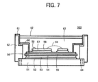
- FIG. 7 is a fragmentary sectional view of a semiconductor module.
- a semiconductor module 500 includes a radiator plate 51, a back electrode film 53 of an insulating substrate with a conductive pattern (hereinafter simply referred to as the insulating substrate 56) which is adhered to the radiator plate 51 with solder 52 between, a semiconductor chip 57 adhered to a conductive pattern 55 formed over the insulating substrate 56 with solder between, a bonding wire 59 which connects a surface electrode (not illustrated) of the semiconductor chip 57 and the conductive pattern 55, a wiring conductor 60 one end of which is connected to the conductive pattern 55, a lead-out terminal 61 to which the other end of the wiring conductor 60 is adhered, a resin case 62 to which the lead-out terminal 61 is adhered, and gel 63 with which the resin case 62 is filled.
- Clamp holes 64 are made in the radiator plate 51 of the semiconductor module 500 for fixing the radiator plate 51 onto a cooling fin (not illustrated).
- the above insulating substrate 56 includes the back electrode film 53, an insulating plate 54 which is a ceramic plate or the like, and the conductive pattern 55 formed over its surface. In many cases, the back electrode film 53 and the conductive pattern 55 are formed by the use of copper foil or the like.
- FIG. 8 is a fragmentary sectional view of the semiconductor module fixed onto a cooling fin.
- the semiconductor module 500 is fixed onto a cooling fin 65 by inserting bolts or the like (not illustrated) into the clamp holes 64 made in a periphery of the radiator plate 51.
- FIG. 9 is a schematic sectional view of a flat radiator plate to which two insulating substrates of the same shape are soldered.
- each insulating substrate 56 is obtained by forming the back electrode film 53 on the back of the insulating plate 54, such as a ceramic plate, and forming the conductive pattern 55 on the front of the insulating plate 54.
- the linear expansion coefficient of the radiator plate 51 made of copper or aluminum is higher than that of each insulating substrate 56, so the radiator plate 51 to which the insulating substrates 56 are soldered curves due to a bimetal effect so that it will be convex on an insulating substrate (insulating substrates 56) side.
- a curve 67 which is convex on the insulating substrate (insulating substrates 56) side is formed on a back 66 of the radiator plate 51. If the radiator plate 51 is attached in this state to the flat cooling fin 65, there will be a big gap 68 in the center of the radiator plate 51, resulting in a decrease in heat radiation efficiency. Measures to prevent this will now be described.
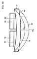
- FIG. 10 is a schematic sectional view of a concave curve formed for canceling out the convex curve of the radiator plate illustrated in FIG. 9 .
- a reverse curve 69 is formed in advance so that the center of the radiator plate 51 will be concave on the insulating substrate (insulating substrates 56) side (which is referred to as reverse curving or initial curving).
- This reverse curve 69 is formed rather sharp so that the radiator plate 51 will not become convex on the insulating substrate (insulating substrates 56) side even after soldering.
- the sharp concave curve 74 becomes a gentle concave curve (not illustrated).
- the radiator plate 73 to which the insulating substrates 71 and 72 are soldered is attached to a cooling fin (not illustrated). As a result, there appears no gap between the radiator plate 73 and the cooling fin.
- a concave curve (reverse curve) is formed in advance on an insulating substrate side of the radiator plate and then the insulating substrate is soldered.
- the radiator plate is kept in a reversely curved state (having a concave curve on the insulating substrate side) even after the soldering.
- the radiator plate 51 curves left-right symmetrically as a result of the soldering so that its center will be convex on the insulating substrate (insulating substrates 56) side.
- a bottom 69a of the concave curve 69 which cancels out this curve is positioned at the center of the radiator plate 51, so the concave curve 69 formed on the radiator plate 51 may be managed at a depth at the center of the radiator plate 51. As a result, management can be exercised easily.
- two insulating substrates of different shapes are soldered to a radiator plate will be described.
- FIG. 12 is a schematic sectional view of a radiator plate to which two insulating substrates of different shapes are soldered.
- insulating substrates 81 and 82 of different shapes are adhered to a flat radiator plate 83 by the use of solder 84
- left-hand and right-hand portions of a convex curve 85 which appears on an insulating substrate (insulating substrates 81 and 82) side after the soldering differ in curvature. Therefore, in order to cancel out the difference in curvature, a concave curve 86 left-hand and right-hand portions of which differ in curvature, that is to say, curvatures of the left-hand and right-hand portions of which are R3 and R4, respectively, may be formed in advance on the radiator plate 83.
- the radiator plate 83 is deformed into the radiator plate 83 having a concave curve 87 a bottom 87a of which is positioned under the insulating substrate 82.
- the curve 86 the left-hand and right-hand portions of which differ in curvature, that is to say, the curvatures of the left-hand and right-hand portions of which are R3 and R4, respectively, may be formed on the radiator plate 83 for canceling out the convex curve 85 which appears as a result of soldering the insulating substrates 81 and 82 of different shapes. Accordingly, the management of the curve 86 is complex.
- FIG. 13 is schematic views of the radiator plate of FIG. 12 before and after being fixed onto a cooling fin.
- Part (a) of FIG. 13 is a schematic view of the radiator plate before being fixed onto the cooling fin.
- Part (b) of FIG. 13 is a schematic view of the radiator plate after being fixed onto the cooling fin.
- the reference sign 92 in FIG. 13 indicates a clamp hole.
- the bottom 87a of the concave curve 87 is positioned under the rigid insulating substrate 82 having high rigidity.
- an end portion of the insulating substrate 82 is lifted up between the insulating substrates 81 and 82 and a gap tends to appear at a contact surface 91 between the radiator plate 83 and a cooling fin 90.
- a curve corresponding to each of the insulating substrates 71 and 72 is formed without taking a curve of the entire radiator plate 73 into consideration. This may lead to considerable curve deformation of the entire radiator plate 73. If considerable initial curving is performed, the following problems, for example, tend to arise. A semiconductor chip mounted over the insulating substrate 71 or 72 at assembly time shifts, or a void appears in solder between the insulating substrate 71 or 72 and the radiator plate 73.
- the insulating substrates 71 and 72 are simply placed over the radiator plate 73. Therefore, as described in FIG. 13 , the bottom of the concave curve may be positioned under the rigid insulating substrate 72 having high rigidity. In that case, stress concentrates in the clearance 75 between the insulating substrates 71 and 72 having low rigidity and a crack tends to appear in solder by which the insulating substrate 72 is adhered to the radiator plate 73. In addition, an end portion of the insulating substrate 72 is lifted up in the clearance 75 between the insulating substrates 71 and 72 and a gap tends to appear between the radiator plate 73 and the cooling fin.
- the above PTL2 does not state that when the insulating substrates of different shapes are soldered to the radiator plate in order to prevent the above troubles, a bottom of the curve (initial curving) formed on the radiator plate before the soldering is positioned under clearance between the insulating substrate.
- An object of the present invention is to solve the above problems and to provide a semiconductor module radiator plate fabrication method, a radiator plate, and a semiconductor module using such a radiator plate in which, at the time of soldering to the radiator plate a plurality of insulating substrates of different shapes, such as a plurality of insulating substrates which differ in area, a plurality of insulating substrates which are equal in area and which differ in external shape, or a plurality of insulating substrates which differ in area and external shape, a curve (initial curving) formed on the radiator plate before the soldering can be managed easily, in which, at the time of soldering to the radiator plate a plurality of insulating substrates of different shapes, such as a plurality of insulating substrates which differ in area, a plurality of insulating substrates which are equal in area and which differ in external shape, or a plurality of insulating substrates which differ in area and external shape, the appearance of a crack in solder can be prevented, and in which,
- a semiconductor module radiator plate fabrication method including soldering a plurality of insulating substrates of different shapes to a flat radiator plate to form a convex curve on an insulating substrate side of the radiator plate, obtaining a first concave curve by reversing the convex curve, setting a concave curve of a radiator plate after soldering, positioning a bottom of the curve under clearance between the plurality of insulating substrates, and setting a second concave curve on the insulating substrate side, adding the first curve and the second curve to calculate a third concave curve on the insulating substrate side, and forming the third curve on a flat plate to form a radiator plate before soldering.
- a bottom of the third curve be positioned under an insulating substrate which is the largest in area of the plurality of insulating substrates of different shapes and that a curvature of a portion of the radiator plate positioned under an insulating substrate which is the smallest in area of the plurality of insulating substrates of different shapes be smaller than a curvature of a portion of the radiator plate positioned under the insulating substrate which is the largest in area of the plurality of insulating substrates of different shapes.
- a curve of the radiator plate included in the semiconductor module be concave on an insulating substrate side and that a bottom of the concave curve be positioned under clearance between the plurality of insulating substrates.
- a material for the above semiconductor module radiator plate be copper or a copper alloy.
- a material for insulating plates used as the plurality of insulating substrates be alumina, aluminum nitride, or silicon nitride.
- a third concave curve is formed in advance on an insulating substrate side of the radiator plate.
- the third curve is determined by adding a second concave curve which is expected at the time of actually soldering the insulating substrates of different shapes to the radiator plate to a second concave curve obtained by moving upside down a convex curve which appears at the time of soldering the insulating substrates of different shapes to a flat radiator plate.
- a bottom of the third curve is positioned under a large insulating substrate and a curvature of a portion of the third curve for which the distance between this bottom and a reference point determined on the basis of the clamping of the radiator plate is longer is made smaller than a curvature of a portion of the third curve for which the distance between the bottom and a reference point determined on the basis of the clamping of the radiator plate is shorter.
- a bottom of a concave portion of the radiator plate is positioned between the insulating substrates.
- the third curve is calculated from a first curve found by actual measurement and the set second curve. Accordingly, the management of the third curve is not so complex as the management of conventional curves and is easy.
- FIG. 1 illustrates a semiconductor module radiator plate fabrication method according to a first example, and parts (a) to (d) of FIG. 1 are fragmentary sectional views of steps indicated in order.
- a case where two insulating substrates of different shapes are soldered to a radiator plate is taken as an example.
- the topmost figure illustrates the arrangement of two insulating substrates 1 and 2 of different shapes and a radiator plate 3. In the following description each radiator plate is indicated uniformly by the numeral 3.
- the flat radiator plate 3 and the two insulating substrates 1 and 2 of different shapes which differ in area are prepared for data acquisition.
- the insulating substrates 1 and 2 are soldered to determined positions on one of the radiator plate 3.
- a convex curve 4 with a top 4a formed on an insulating substrate (insulating substrates 1 and 2) side of the radiator plate 3 is measured.
- the shape from above of each of the insulating substrates 1 and 2 and the radiator plate 3 is rectangular.
- each of the insulating substrates 1 and 2 is arranged so that its one side will be parallel to a long side of the radiator plate 3.
- the top 4a of the convex curve 4 is positioned under the large insulating substrate 2.
- the distance L11 between the top 4a and a reference point 5a on a small insulating substrate 1 side is longer than the distance L21 between the top 4a and a reference point 5b on a large insulating substrate 2 side.
- a concave curve is obtained as a first curve 6 by moving the measured convex curve 4 illustrated in part (a) of FIG. 1 upside down (concave curve obtained by reversing the curve 4 with respect to the X-X line or an X-Y plane including the reference points 5a and 5b).
- a bottom 6a of the first curve 6 is positioned under the large insulating substrate 2.
- a curvature R11 of a portion of the first curve 6 for which the distance (L11) between the bottom 6a of the first curve 6 and the reference point 5a is longer is smaller than a curvature R21 of a portion of the first curve 6 for which the distance (L21) between the bottom 6a of the first curve 6 and the reference point 5b is shorter. That is to say, curvature R11 (gentle curve) ⁇ curvature R21 (sharp curve).
- a concave curve of the radiator plate 3 to be realized at the time of soldering the insulating substrates 1 and 2 to the determined positions is specified.
- the specified concave curve is set as a second curve 7.
- the second curve 7 is specified so that a bottom 7a of the second curve 7 will be positioned under clearance 8 between the two insulating substrates 1 and 2 and so that the second curve 7 will be concave on the insulating substrate (insulating substrates 1 and 2) side.
- the second curve 7 is practically identical to a third curve 11 formed at the time of actually soldering the insulating substrates 1 and 2 of different shapes to the radiator plate 3.
- the bottom 7a of the second curve 7 be positioned under clearance between, for example, the insulating substrates 1 and 2 which are near the center of the radiator plate 3.
- two straight lines 9 and 10 may be drawn between the bottom 7a of the second curve 7 and the reference points 5a and 5b. In this case, a second plane is obtained as a surface.
- the radiator plate 3 is convexly curved upward by the two straight lines 9 and 10, then clearance appears at the time of fixing the radiator plate 3 onto a cooling fin. It is preferable to avoid the appearance of clearance.
- the second curve 7 is represented by the two straight lines 9 and 10, then the relationship "curvature R1 ⁇ curvature R2" regarding a third curve 11 illustrated in part (d) of FIG. 1 becomes more significant.
- a profile of the second curve 7 is superimposed on a profile of the first curve 6.
- an addition is performed to calculate a profile of the third concave curve 11.
- a bottom 11a of the third curve 11 is positioned near the bottom 6a of the first curve 6.
- the third curve 11 has a shape for canceling out a convex curve formed on the insulating substrate (insulating substrates 1 and 2) side at the time of soldering and for forming the second concave curve 7.
- the third curve 11 is a curve of the radiator plate 3 before soldering (initial curving).
- a curvature R1 of a portion of the third curve 11 for which the distance (L1) between the bottom 11a of the third curve 11 and the reference point 5a is longer is smaller than a curvature R2 of a portion of the third curve 11 for which the distance (L2) between the bottom 11a of the third curve 11 and the reference point 5b is shorter. That is to say, curvature R1 (gentle curve) ⁇ curvature R2 (sharp curve).
- the position of the bottom 11a of the third curve 11 is approximately identical to that of the bottom 6a of the first curve 6.
- the radiator plate 3 having a fourth curve 21 close to the second curve 7 is obtained.
- This radiator plate 3 is included in a semiconductor module.
- the shape of the third curve 11 is determined from a curve of the entire radiator plate 3.
- curves are determined according to insulating substrates and these curves are combined to determine an entire curve.
- the third curve 11 does not become too sharp. Accordingly, when the radiator plate 3 is fixed onto the cooling fin 33, it is possible to prevent a crack from appearing in solder between the insulating substrates 1 and 2 and the radiator plate 3.
- the third curve 11 is calculated from the first curve 6 found by the experiment and the set second curve 7. Therefore, the management of the third curve 11 is not so complex as the management of conventional curves and is easy.
- FIG. 3 illustrates views which illustrate the structure of a semiconductor module radiator plate according to a second example.
- Part (a) of FIG. 3 is a fragmentary plan view which illustrates the structure of a semiconductor module radiator plate according to a second example.
- Part (b) of FIG. 3 is a fragmentary sectional view taken along lines X-X of part (a) of FIG. 3 .
- Part (d) of FIG. 1 illustrates only the curve in the X direction.
- the fabrication method according to the first example is extended to a surface.
- a curve in the Y direction is also measured by the same technique and a two-dimensional curve illustrated in part (a) of FIG. 3 is obtained.
- a bottom 11a of the two-dimensional curve is the same as the bottom 11a of the third curve 11.
- the third curve 11 is also used as a two-dimensional curve.
- the numeral 16 in part (a) of FIG. 3 indicates a contour line of the third curve 11.
- the bottom 11a of the third curve 11 is positioned near the bottom 6a of the above first curve 6 and a curvature R1 of a portion of the third curve 11 for which the distance (L1) between the bottom 11a of the third curve 11 and the reference point 5a is longer is smaller than a curvature R2 of a portion of the third curve 11 for which the distance (L2) between the bottom 11a of the third curve 11 and the reference point 5b is shorter (R1 ⁇ R2).
- FIG. 4 illustrates views for describing a concrete method for fabricating the radiator plate illustrated in FIG. 3 .
- Part (a) of FIG. 4 is a view which illustrates a flat plate put between dies.
- Part (b) of FIG. 4 is a view which illustrates a radiator plate fabricated by pressing the flat plate between the dies.
- a concave die 17 and a convex die 18 each having the above third curve 11 are made.
- a flat plat 19 made of copper or a copper alloy is put between the concave die 17 and the convex die 18 and is pressed between them. By doing so, the radiator plate having the third curve 11 is fabricated.
- the clamp holes 5 are made in the periphery of the radiator plate 3.
- the straight lines which connect the centers of the clamp holes 5 are needed for determining the reference points 5a and 5b (see FIGS. 2 and 3 ) used for measuring the curvatures R1 and R2 of the third curve 11.
- FIG. 5 illustrates fragmentary sectional views of a semiconductor module according to a third example.
- Part (a) of FIG. 5 is a fragmentary sectional view of an entire semiconductor module.
- Part (b) of FIG. 5 is a fragmentary sectional view of a curve of a back of the radiator plate of part (a) of FIG. 5 .
- the radiator plate 3 illustrated in FIG. 3 is used in a semiconductor module 100.
- the semiconductor module 100 includes the radiator plate 3, insulating substrates with a conductive pattern (above insulating substrates 1 and 2) back conductive films (not illustrated) of which are adhered to the radiator plate 3 with solder 25 between, semiconductor chips 27 adhered to a conductive pattern (not illustrated) of the radiator plate 3 with solder 26 between, bonding wires 28 which connect surface electrodes (not illustrated) of the semiconductor chips 27 and the conductive patterns, wiring conductors 29 one end of each of which is connected to a conductive pattern, lead-out terminals 30 to each of which the other end of each of the wiring conductor 29 is adhered, a resin case 31 to which the lead-out terminals 30 are adhered, and gel 32 with which the resin case 31 is filled.
- the insulating substrates 1 and 2 are soldered to the radiator plate 3 having the third curve. By doing so, a bottom 21a of the fourth concave curve 21 of the radiator plate 3 is positioned under the clearance 8 between the insulating substrates 1 and 2.
- the fourth curve 21 is very close to the above second curve 7.
- FIG. 6 illustrates fragmentary sectional views of the semiconductor module radiator plate of FIG. 5 fixed onto a cooling fin by the use of clamp holes.
- Part (a) of FIG. 6 is a fragmentary sectional view of the whole of the semiconductor module and a cooling fin.
- Part (b) of FIG. 6 is a fragmentary sectional view of the curve of the back of the radiator plate.
- Part (c) of FIG. 6 is a fragmentary sectional view which illustrates the back of the radiator plate in a flat state after fixing the radiator plate onto a cooling fin.
- the bottom 21a of the fourth concave curve 21 of the radiator plate 3 is positioned under the clearance 8 between the insulating substrates 1 and 2, so the radiator plate 3 having low rigidity is pressed against a cooling fin 33 with the bottom 21a of the fourth curve 21 and the clamp holes 5 of the radiator plate 3 as supporting points. At this time there is no supporting point (bottom 21a of the fourth curve 21) in the insulating substrate 2 having high rigidity. As a result, the whole of the back 15 of the radiator plate 3 adheres closely to the cooling fin 33 and the appearance of a gap between the radiator plate 3 and the cooling fin 33 is prevented.
- the shape of the third curve 11 is determined from a curve of the entire radiator plate 3, so the third curve 11 does not become too sharp. Accordingly, when the radiator plate 3 is fixed onto the cooling fin 33, the appearance of a crack in the solder 25 between the insulating substrates 1 and 2 and the radiator plate 3 is prevented.
- a material for the above radiator plate 3 is copper, a copper alloy (C19220 or C19210, for example), or the like. Furthermore, insulating plates made of alumina, aluminum nitride, silicon nitride, or the like are used as the insulating substrates 1 and 2 mounted over the radiator plate 3.
Landscapes
- Engineering & Computer Science (AREA)
- Mechanical Engineering (AREA)
- Physics & Mathematics (AREA)
- Thermal Sciences (AREA)
- General Engineering & Computer Science (AREA)
- Cooling Or The Like Of Semiconductors Or Solid State Devices (AREA)
- Chemical & Material Sciences (AREA)
- Ceramic Engineering (AREA)
Abstract
Description
- The embodiments discussed herein are related to a semiconductor module radiator plate fabrication method, a radiator plate, and a semiconductor module using such a radiator plate.
-
FIG. 7 is a fragmentary sectional view of a semiconductor module. Asemiconductor module 500 includes aradiator plate 51, aback electrode film 53 of an insulating substrate with a conductive pattern (hereinafter simply referred to as the insulating substrate 56) which is adhered to theradiator plate 51 withsolder 52 between, asemiconductor chip 57 adhered to aconductive pattern 55 formed over theinsulating substrate 56 with solder between, abonding wire 59 which connects a surface electrode (not illustrated) of thesemiconductor chip 57 and theconductive pattern 55, awiring conductor 60 one end of which is connected to theconductive pattern 55, a lead-outterminal 61 to which the other end of thewiring conductor 60 is adhered, aresin case 62 to which the lead-outterminal 61 is adhered, andgel 63 with which theresin case 62 is filled.Clamp holes 64 are made in theradiator plate 51 of thesemiconductor module 500 for fixing theradiator plate 51 onto a cooling fin (not illustrated). The aboveinsulating substrate 56 includes theback electrode film 53, aninsulating plate 54 which is a ceramic plate or the like, and theconductive pattern 55 formed over its surface. In many cases, theback electrode film 53 and theconductive pattern 55 are formed by the use of copper foil or the like. -
FIG. 8 is a fragmentary sectional view of the semiconductor module fixed onto a cooling fin. Thesemiconductor module 500 is fixed onto acooling fin 65 by inserting bolts or the like (not illustrated) into theclamp holes 64 made in a periphery of theradiator plate 51. -
FIG. 9 is a schematic sectional view of a flat radiator plate to which two insulating substrates of the same shape are soldered. As illustrated inFIG. 7 , eachinsulating substrate 56 is obtained by forming theback electrode film 53 on the back of theinsulating plate 54, such as a ceramic plate, and forming theconductive pattern 55 on the front of theinsulating plate 54. The linear expansion coefficient of theradiator plate 51 made of copper or aluminum is higher than that of eachinsulating substrate 56, so theradiator plate 51 to which theinsulating substrates 56 are soldered curves due to a bimetal effect so that it will be convex on an insulating substrate (insulating substrates 56) side. That is to say, acurve 67 which is convex on the insulating substrate (insulating substrates 56) side is formed on aback 66 of theradiator plate 51. If theradiator plate 51 is attached in this state to theflat cooling fin 65, there will be abig gap 68 in the center of theradiator plate 51, resulting in a decrease in heat radiation efficiency. Measures to prevent this will now be described. -
FIG. 10 is a schematic sectional view of a concave curve formed for canceling out the convex curve of the radiator plate illustrated inFIG. 9 . - In order to cancel out the convex
curve 67 illustrated inFIG. 9 , areverse curve 69 is formed in advance so that the center of theradiator plate 51 will be concave on the insulating substrate (insulating substrates 56) side (which is referred to as reverse curving or initial curving). Thisreverse curve 69 is formed rather sharp so that theradiator plate 51 will not become convex on the insulating substrate (insulating substrates 56) side even after soldering. - When the
insulating substrates 56 are soldered to theradiator plate 51 by which thereverse curve 69 indicated by a dashed line is formed, theconvex curve 67 illustrated inFIG. 9 is canceled out and acurve 70 which is concave on the insulating substrate (insulating substrates 56) side is formed. When theradiator plate 51 is attached in this state to thecooling fin 65 by the use of theclamp holes 64, the center of the radiator plate 51 (bottom 70a of the concave curve 70) touches thecooling fin 65, both ends of theradiator plate 51 are pressed against thecooling fin 65 with the bottom 70a as a supporting point, and the whole of theback 66 of theradiator plate 51 adheres to thecooling fin 65. - Furthermore, according to PTL1, as illustrated in
FIG. 11 , ifinsulating substrates radiator plate 73, asharp curve 74 includingconcave curves insulating substrates radiator plate 73. It is assumed that the sizes of thecurves insulating substrates radiator plate 73, the sharpconcave curve 74 becomes a gentle concave curve (not illustrated). Theradiator plate 73 to which theinsulating substrates radiator plate 73 and the cooling fin. - In addition, according to PTL2 (not illustrated), when an insulating substrate is adhered to a radiator plate by the use of solder, a concave curve (reverse curve) is formed in advance on an insulating substrate side of the radiator plate and then the insulating substrate is soldered. By doing so, the radiator plate is kept in a reversely curved state (having a concave curve on the insulating substrate side) even after the soldering. By attaching the radiator plate in a reversely curved state to a cooling fin, there appears no gap between the radiator plate and the cooling fin.
-
- PTL1: Japanese Laid-open Patent Publication No.
2007-88045 - PTL2: Japanese Laid-open Patent Publication No.
2008-91959 - In
FIG. 10 , if theinsulating substrates 56 soldered to theradiator plate 51 have the same shape and are arranged left-right symmetrically, then theradiator plate 51 curves left-right symmetrically as a result of the soldering so that its center will be convex on the insulating substrate (insulating substrates 56) side. Abottom 69a of theconcave curve 69 which cancels out this curve is positioned at the center of theradiator plate 51, so theconcave curve 69 formed on theradiator plate 51 may be managed at a depth at the center of theradiator plate 51. As a result, management can be exercised easily. Next, a case where two insulating substrates of different shapes are soldered to a radiator plate will be described. -
FIG. 12 is a schematic sectional view of a radiator plate to which two insulating substrates of different shapes are soldered. Wheninsulating substrates flat radiator plate 83 by the use ofsolder 84, left-hand and right-hand portions of aconvex curve 85 which appears on an insulating substrate (insulating substrates 81 and 82) side after the soldering differ in curvature. Therefore, in order to cancel out the difference in curvature, aconcave curve 86 left-hand and right-hand portions of which differ in curvature, that is to say, curvatures of the left-hand and right-hand portions of which are R3 and R4, respectively, may be formed in advance on theradiator plate 83. - When the
insulating substrates radiator plate 83 having thecurve 86, theradiator plate 83 is deformed into theradiator plate 83 having aconcave curve 87 abottom 87a of which is positioned under theinsulating substrate 82. - With the method of forming the
concave curve 86 in this way, a position at which the left-hand and right-hand portions of thecurve 86 which differ in curvature, that is to say, the curvatures of which are R3 and R4, respectively, connect deviates from the center and becomes unclear. Accordingly, it is difficult to manage thecurve 86. - Furthermore, the
curve 86 the left-hand and right-hand portions of which differ in curvature, that is to say, the curvatures of the left-hand and right-hand portions of which are R3 and R4, respectively, may be formed on theradiator plate 83 for canceling out theconvex curve 85 which appears as a result of soldering theinsulating substrates curve 86 is complex. -
FIG. 13 is schematic views of the radiator plate ofFIG. 12 before and after being fixed onto a cooling fin. Part (a) ofFIG. 13 is a schematic view of the radiator plate before being fixed onto the cooling fin. Part (b) ofFIG. 13 is a schematic view of the radiator plate after being fixed onto the cooling fin. Thereference sign 92 inFIG. 13 indicates a clamp hole. - As illustrated in part (a) of
FIG. 13 , thebottom 87a of theconcave curve 87 is positioned under the rigidinsulating substrate 82 having high rigidity. As a result, stress concentrates inclearance 88 having low rigidity between theinsulating substrates FIG. 13 , acrack 89 tends to appear in thesolder 84, or a crack (not illustrated) tends to appear in theinsulating substrate insulating substrate 82 is lifted up between theinsulating substrates contact surface 91 between theradiator plate 83 and acooling fin 90. - According to the above PTL1, a curve corresponding to each of the
insulating substrates entire radiator plate 73 into consideration. This may lead to considerable curve deformation of theentire radiator plate 73. If considerable initial curving is performed, the following problems, for example, tend to arise. A semiconductor chip mounted over theinsulating substrate insulating substrate radiator plate 73. - Furthermore, the
insulating substrates radiator plate 73. Therefore, as described inFIG. 13 , the bottom of the concave curve may be positioned under the rigidinsulating substrate 72 having high rigidity. In that case, stress concentrates in theclearance 75 between theinsulating substrates insulating substrate 72 is adhered to theradiator plate 73. In addition, an end portion of theinsulating substrate 72 is lifted up in theclearance 75 between theinsulating substrates radiator plate 73 and the cooling fin. - Furthermore, the above PTL2 does not state that when the insulating substrates of different shapes are soldered to the radiator plate in order to prevent the above troubles, a bottom of the curve (initial curving) formed on the radiator plate before the soldering is positioned under clearance between the insulating substrate.
- An object of the present invention is to solve the above problems and to provide a semiconductor module radiator plate fabrication method, a radiator plate, and a semiconductor module using such a radiator plate in which, at the time of soldering to the radiator plate a plurality of insulating substrates of different shapes, such as a plurality of insulating substrates which differ in area, a plurality of insulating substrates which are equal in area and which differ in external shape, or a plurality of insulating substrates which differ in area and external shape, a curve (initial curving) formed on the radiator plate before the soldering can be managed easily, in which, at the time of soldering to the radiator plate a plurality of insulating substrates of different shapes, such as a plurality of insulating substrates which differ in area, a plurality of insulating substrates which are equal in area and which differ in external shape, or a plurality of insulating substrates which differ in area and external shape, the appearance of a crack in solder can be prevented, and in which, at the time of soldering to the radiator plate a plurality of insulating substrates of different shapes, such as a plurality of insulating substrates which differ in area, a plurality of insulating substrates which are equal in area and which differ in external shape, or a plurality of insulating substrates which differ in area and external shape, a gap between the radiator plate and a cooling fin can be made narrow.
- In order to achieve the above object, there is provided a semiconductor module radiator plate fabrication method including soldering a plurality of insulating substrates of different shapes to a flat radiator plate to form a convex curve on an insulating substrate side of the radiator plate, obtaining a first concave curve by reversing the convex curve, setting a concave curve of a radiator plate after soldering, positioning a bottom of the curve under clearance between the plurality of insulating substrates, and setting a second concave curve on the insulating substrate side, adding the first curve and the second curve to calculate a third concave curve on the insulating substrate side, and forming the third curve on a flat plate to form a radiator plate before soldering.
- In addition, on a semiconductor module radiator plate fabricated by the above semiconductor module radiator plate fabrication method, it is desirable that a bottom of the third curve be positioned under an insulating substrate which is the largest in area of the plurality of insulating substrates of different shapes and that a curvature of a portion of the radiator plate positioned under an insulating substrate which is the smallest in area of the plurality of insulating substrates of different shapes be smaller than a curvature of a portion of the radiator plate positioned under the insulating substrate which is the largest in area of the plurality of insulating substrates of different shapes.
- Furthermore, in a semiconductor module fabricated by the use of the above semiconductor module radiator plate, it is desirable that a curve of the radiator plate included in the semiconductor module be concave on an insulating substrate side and that a bottom of the concave curve be positioned under clearance between the plurality of insulating substrates.
- Moreover, it is desirable that a material for the above semiconductor module radiator plate be copper or a copper alloy.
- In addition, it is desirable that in the above semiconductor module a material for insulating plates used as the plurality of insulating substrates be alumina, aluminum nitride, or silicon nitride.
- According to the present invention, when insulating substrates of different shapes are soldered to a radiator plate, a third concave curve is formed in advance on an insulating substrate side of the radiator plate. The third curve is determined by adding a second concave curve which is expected at the time of actually soldering the insulating substrates of different shapes to the radiator plate to a second concave curve obtained by moving upside down a convex curve which appears at the time of soldering the insulating substrates of different shapes to a flat radiator plate. A bottom of the third curve is positioned under a large insulating substrate and a curvature of a portion of the third curve for which the distance between this bottom and a reference point determined on the basis of the clamping of the radiator plate is longer is made smaller than a curvature of a portion of the third curve for which the distance between the bottom and a reference point determined on the basis of the clamping of the radiator plate is shorter.
- A bottom of a concave portion of the radiator plate is positioned between the insulating substrates. As a result, when the radiator plate is attached to a cooling fin, a crack does not appear in solder. In addition, a gap between the radiator plate and the cooling fin is made narrow. Accordingly, heat radiation properties can be improved.
- Furthermore, the third curve is calculated from a first curve found by actual measurement and the set second curve. Accordingly, the management of the third curve is not so complex as the management of conventional curves and is easy.
- The above and other objects, features and advantages of the present invention will become apparent from the following description when taken in conjunction with the accompanying drawings which illustrate preferred embodiments of the present invention by way of example.
-
- [
FIG. 1] FIG. 1 illustrates a semiconductor module radiator plate fabrication method according to a first example, where (a) to (d) are fragmentary sectional views of steps indicated in order. - [
FIG. 2] FIG. 2 is a fragmentary plan view which illustrates a state in which, as a result of soldering two insulating substrates of different shapes to a flat radiator plate, a convex curve is formed on an insulating substrate side of the radiator plate. - [
FIG. 3] FIG. 3 illustrates the structure of a semiconductor module radiator plate according to a second example, where (a) is a fragmentary plan view, and (b) is a fragmentary sectional view taken along lines X-X of (a). - [
FIG. 4] FIG. 4 illustrates views for describing a concrete method for fabricating the radiator plate illustrated inFIG. 3 , where (a) is a view which illustrates a flat plate put between dies, and (b) is a view which illustrates a radiator plate fabricated by pressing the flat plate between the dies. - [
FIG. 5] FIG. 5 illustrates fragmentary sectional views of a semiconductor module according to a third example, where (a) is a fragmentary sectional view of an entire semiconductor module, and (b) is a fragmentary sectional view of a curve of a back of the radiator plate of (a). - [
FIG. 6] FIG. 6 illustrates fragmentary sectional views of the semiconductor module radiator plate ofFIG. 5 fixed onto a cooling fin by the use of clamp holes, where (a) is a fragmentary sectional view of the whole of the semiconductor module and a cooling fin, (b) is a fragmentary sectional view of the curve of the back of the radiator plate, and (c) is a fragmentary sectional view which illustrates the back of the radiator plate in a flat state after fixing the radiator plate onto a cooling fin. - [
FIG. 7] FIG. 7 is a fragmentary sectional view of a semiconductor module. - [
FIG. 8] FIG. 8 is a fragmentary sectional view of the semiconductor module fixed onto a cooling fin. - [
FIG. 9] FIG. 9 is a schematic sectional view of a flat radiator plate to which two insulating substrates of the same shape are soldered. - [
FIG. 10] FIG. 10 is a schematic sectional view of a concave curve formed for canceling out the convex curve of the radiator plate illustrated inFIG. 9 . - [
FIG. 11] FIG. 11 is a schematic sectional view of a curve of a radiator plate before soldering insulating substrates of different shapes to the radiator plate, which is described in PTL1. - [
FIG. 12] FIG. 12 is a schematic sectional view of a radiator plate to which two insulating substrates of different shapes are soldered. - [
FIG. 13] FIG. 13 illustrates schematic views of the radiator plate ofFIG. 12 before and after being fixed onto a cooling fin, where (a) is a schematic view of the radiator plate before being fixed onto the cooling fin, and (b) is a schematic view of the radiator plate after being fixed onto the cooling fin. - Embodiments will be described by the following examples.
-
FIG. 1 illustrates a semiconductor module radiator plate fabrication method according to a first example, and parts (a) to (d) ofFIG. 1 are fragmentary sectional views of steps indicated in order. A case where two insulating substrates of different shapes are soldered to a radiator plate is taken as an example. The topmost figure illustrates the arrangement of two insulatingsubstrates radiator plate 3. In the following description each radiator plate is indicated uniformly by thenumeral 3. - First the
flat radiator plate 3 and the two insulatingsubstrates substrates radiator plate 3. As illustrated in part (a) ofFIG. 1 , a convex curve 4 with a top 4a formed on an insulating substrate (insulatingsubstrates 1 and 2) side of theradiator plate 3 is measured. In this case, the shape from above of each of the insulatingsubstrates radiator plate 3 is rectangular. Furthermore, each of the insulatingsubstrates radiator plate 3. - The top 4a of the convex curve 4 is positioned under the large insulating
substrate 2. The distance L11 between the top 4a and areference point 5a on a smallinsulating substrate 1 side is longer than the distance L21 between the top 4a and areference point 5b on a largeinsulating substrate 2 side. - As illustrated in
FIG. 2 , to measure the convex curve 4, the intersections on a back 15 side of theradiator plate 3 of straight lines (in a Y direction) which connect the centers ofclamp holes 5 made in a periphery of theradiator plate 3 and a straight line drawn in an X direction through the top 4a of the curve 4 are used asreference points reference points - Next, as illustrated in part (b) of
FIG. 1 , a concave curve is obtained as a first curve 6 by moving the measured convex curve 4 illustrated in part (a) ofFIG. 1 upside down (concave curve obtained by reversing the curve 4 with respect to the X-X line or an X-Y plane including thereference points substrate 2. A curvature R11 of a portion of the first curve 6 for which the distance (L11) between the bottom 6a of the first curve 6 and thereference point 5a is longer is smaller than a curvature R21 of a portion of the first curve 6 for which the distance (L21) between the bottom 6a of the first curve 6 and thereference point 5b is shorter. That is to say, curvature R11 (gentle curve) < curvature R21 (sharp curve). - Next, as illustrated in part (c) of
FIG. 1 , a concave curve of theradiator plate 3 to be realized at the time of soldering the insulatingsubstrates second curve 7. In this case, thesecond curve 7 is specified so that a bottom 7a of thesecond curve 7 will be positioned underclearance 8 between the two insulatingsubstrates second curve 7 will be concave on the insulating substrate (insulatingsubstrates 1 and 2) side. Thesecond curve 7 is practically identical to athird curve 11 formed at the time of actually soldering the insulatingsubstrates radiator plate 3. When three or more insulating substrates are soldered to theradiator plate 3, it is desirable that the bottom 7a of thesecond curve 7 be positioned under clearance between, for example, the insulatingsubstrates radiator plate 3. Furthermore, as indicated by dotted lines, twostraight lines 9 and 10 may be drawn between the bottom 7a of thesecond curve 7 and thereference points radiator plate 3 is convexly curved upward by the twostraight lines 9 and 10, then clearance appears at the time of fixing theradiator plate 3 onto a cooling fin. It is preferable to avoid the appearance of clearance. If thesecond curve 7 is represented by the twostraight lines 9 and 10, then the relationship "curvature R1 < curvature R2" regarding athird curve 11 illustrated in part (d) ofFIG. 1 becomes more significant. - Next, as illustrated in part (d) of
FIG. 1 , a profile of thesecond curve 7 is superimposed on a profile of the first curve 6. By doing so, an addition is performed to calculate a profile of the thirdconcave curve 11. A bottom 11a of thethird curve 11 is positioned near the bottom 6a of the first curve 6. Thethird curve 11 has a shape for canceling out a convex curve formed on the insulating substrate (insulatingsubstrates 1 and 2) side at the time of soldering and for forming the secondconcave curve 7. Thethird curve 11 is a curve of theradiator plate 3 before soldering (initial curving). A curvature R1 of a portion of thethird curve 11 for which the distance (L1) between the bottom 11a of thethird curve 11 and thereference point 5a is longer is smaller than a curvature R2 of a portion of thethird curve 11 for which the distance (L2) between the bottom 11a of thethird curve 11 and thereference point 5b is shorter. That is to say, curvature R1 (gentle curve) < curvature R2 (sharp curve). - In addition, the position of the bottom 11a of the
third curve 11 is approximately identical to that of the bottom 6a of the first curve 6. - When the insulating
substrates radiator plate 3 having thethird curve 11, then theradiator plate 3 having a fourth curve 21 (seeFIG. 5 ) close to thesecond curve 7 is obtained. Thisradiator plate 3 is included in a semiconductor module. - For the sake of simplicity one dimension has been described above, but in reality concave curves are two-dimensionally measured to obtain the first curve 6, the
second curve 7, and thethird curve 11. - In this example, as stated above, the shape of the
third curve 11 is determined from a curve of theentire radiator plate 3. With PTL1, curves are determined according to insulating substrates and these curves are combined to determine an entire curve. In this example, on the other hand, thethird curve 11 does not become too sharp. Accordingly, when theradiator plate 3 is fixed onto the coolingfin 33, it is possible to prevent a crack from appearing in solder between the insulatingsubstrates radiator plate 3. - Furthermore, as stated above, the
third curve 11 is calculated from the first curve 6 found by the experiment and the setsecond curve 7. Therefore, the management of thethird curve 11 is not so complex as the management of conventional curves and is easy. -
FIG. 3 illustrates views which illustrate the structure of a semiconductor module radiator plate according to a second example. Part (a) ofFIG. 3 is a fragmentary plan view which illustrates the structure of a semiconductor module radiator plate according to a second example. Part (b) ofFIG. 3 is a fragmentary sectional view taken along lines X-X of part (a) ofFIG. 3 . - Part (d) of
FIG. 1 illustrates only the curve in the X direction. In this example, however, the fabrication method according to the first example is extended to a surface. A curve in the Y direction is also measured by the same technique and a two-dimensional curve illustrated in part (a) ofFIG. 3 is obtained. A bottom 11a of the two-dimensional curve is the same as the bottom 11a of thethird curve 11. In this case, it is assumed that thethird curve 11 is also used as a two-dimensional curve. The numeral 16 in part (a) ofFIG. 3 indicates a contour line of thethird curve 11. - On the
radiator plate 3 inFIG. 3 on which the thirdconcave curve 11 is formed, the bottom 11a of thethird curve 11 is positioned near the bottom 6a of the above first curve 6 and a curvature R1 of a portion of thethird curve 11 for which the distance (L1) between the bottom 11a of thethird curve 11 and thereference point 5a is longer is smaller than a curvature R2 of a portion of thethird curve 11 for which the distance (L2) between the bottom 11a of thethird curve 11 and thereference point 5b is shorter (R1<R2). One reason for this is that the curvature R11 of the portion of the first curve 6 in part (b) ofFIG. 1 for which the distance (L11) between the bottom 6a of the first curve 6 and thereference point 5a is longer is smaller than the curvature R21 of the portion of the first curve 6 for which the distance (L21) between the bottom 6a of the first curve 6 and thereference point 5b is shorter. -
FIG. 4 illustrates views for describing a concrete method for fabricating the radiator plate illustrated inFIG. 3 . Part (a) ofFIG. 4 is a view which illustrates a flat plate put between dies. Part (b) ofFIG. 4 is a view which illustrates a radiator plate fabricated by pressing the flat plate between the dies. Aconcave die 17 and aconvex die 18 each having the abovethird curve 11 are made. Aflat plat 19 made of copper or a copper alloy is put between theconcave die 17 and theconvex die 18 and is pressed between them. By doing so, the radiator plate having thethird curve 11 is fabricated. The clamp holes 5 are made in the periphery of theradiator plate 3. The straight lines which connect the centers of the clamp holes 5 are needed for determining thereference points FIGS. 2 and3 ) used for measuring the curvatures R1 and R2 of thethird curve 11. -
FIG. 5 illustrates fragmentary sectional views of a semiconductor module according to a third example. Part (a) ofFIG. 5 is a fragmentary sectional view of an entire semiconductor module. Part (b) ofFIG. 5 is a fragmentary sectional view of a curve of a back of the radiator plate of part (a) ofFIG. 5 . Theradiator plate 3 illustrated inFIG. 3 is used in asemiconductor module 100. - The
semiconductor module 100 includes theradiator plate 3, insulating substrates with a conductive pattern (above insulatingsubstrates 1 and 2) back conductive films (not illustrated) of which are adhered to theradiator plate 3 withsolder 25 between,semiconductor chips 27 adhered to a conductive pattern (not illustrated) of theradiator plate 3 withsolder 26 between,bonding wires 28 which connect surface electrodes (not illustrated) of the semiconductor chips 27 and the conductive patterns, wiringconductors 29 one end of each of which is connected to a conductive pattern, lead-outterminals 30 to each of which the other end of each of thewiring conductor 29 is adhered, aresin case 31 to which the lead-outterminals 30 are adhered, andgel 32 with which theresin case 31 is filled. - The insulating
substrates radiator plate 3 having the third curve. By doing so, a bottom 21a of the fourthconcave curve 21 of theradiator plate 3 is positioned under theclearance 8 between the insulatingsubstrates fourth curve 21 is very close to the abovesecond curve 7. -
FIG. 6 illustrates fragmentary sectional views of the semiconductor module radiator plate ofFIG. 5 fixed onto a cooling fin by the use of clamp holes. Part (a) ofFIG. 6 is a fragmentary sectional view of the whole of the semiconductor module and a cooling fin. Part (b) ofFIG. 6 is a fragmentary sectional view of the curve of the back of the radiator plate. Part (c) ofFIG. 6 is a fragmentary sectional view which illustrates the back of the radiator plate in a flat state after fixing the radiator plate onto a cooling fin. - The bottom 21a of the fourth
concave curve 21 of theradiator plate 3 is positioned under theclearance 8 between the insulatingsubstrates radiator plate 3 having low rigidity is pressed against a coolingfin 33 with the bottom 21a of thefourth curve 21 and the clamp holes 5 of theradiator plate 3 as supporting points. At this time there is no supporting point (bottom 21a of the fourth curve 21) in the insulatingsubstrate 2 having high rigidity. As a result, the whole of theback 15 of theradiator plate 3 adheres closely to the coolingfin 33 and the appearance of a gap between theradiator plate 3 and the coolingfin 33 is prevented. - As stated above, in this embodiment the shape of the
third curve 11 is determined from a curve of theentire radiator plate 3, so thethird curve 11 does not become too sharp. Accordingly, when theradiator plate 3 is fixed onto the coolingfin 33, the appearance of a crack in thesolder 25 between the insulatingsubstrates radiator plate 3 is prevented. - A material for the
above radiator plate 3 is copper, a copper alloy (C19220 or C19210, for example), or the like. Furthermore, insulating plates made of alumina, aluminum nitride, silicon nitride, or the like are used as the insulatingsubstrates radiator plate 3. - The foregoing is considered as illustrative only of the principles of the present invention. Further, since numerous modifications and changes will readily occur to those skilled in the art, it is not desired to limit the invention to the exact construction and applications shown and described, and accordingly, all suitable modifications and equivalents may be regarded as falling within the scope of the invention in the appended claims and their equivalents.
-
- 1, 2
- insulating substrate
- 3
- radiator plate
- 4
- convex curve
- 4a
- top
- 5
- clamp hole
- 5a, 5b
- reference point
- 6
- first curve
- 6a, 7a, 11a, 21a
- bottom
- 7
- second curve
- 8
- clearance
- 9, 10
- straight line
- 11
- third curve
- 15
- back
- 16
- contour line
- 17
- concave die
- 18
- convex die
- 19
- flat plate
- 21
- fourth curve
- 25, 26
- solder
- 27
- semiconductor chip
- 28
- bonding wire
- 29
- wiring conductor
- 30
- lead-out terminal
- 31
- resin case
- 32
- gel
- 33
- cooling fin
- 100
- semiconductor module
Claims (5)
- A semiconductor module radiator plate fabrication method comprising:soldering a plurality of insulating substrates of different shapes to a flat radiator plate, and forming a convex curve on an insulating substrate side of the radiator plate;obtaining a first concave curve by reversing the convex curve;setting a second concave curve on an insulating substrate side of a radiator plate after soldering, a bottom of the second concave curve being positioned under clearance between the plurality of insulating substrates;adding the first curve and the second curve to calculate a third concave curve on the insulating substrate side; andforming the third curve on a flat plate to form a radiator plate before soldering.
- A semiconductor module radiator plate fabricated by the semiconductor module radiator plate fabrication method according to claim 1, wherein:a bottom of the third curve is positioned under an insulating substrate which is the largest in area of the plurality of insulating substrates of different shapes; anda curvature of a portion of the radiator plate positioned under an insulating substrate which is the smallest in area of the plurality of insulating substrates of different shapes is smaller than a curvature of a portion of the radiator plate positioned under the insulating substrate which is the largest in area of the plurality of insulating substrates of different shapes.
- A semiconductor module fabricated by the use of the semiconductor module radiator plate according to claim 2, wherein:a curve of the radiator plate included in the semiconductor module is concave on an insulating substrate side; anda bottom of the concave curve is positioned under clearance between the plurality of insulating substrates.
- The semiconductor module radiator plate according to claim 2, wherein a material is copper or a copper alloy.
- The semiconductor module according to claim 3, wherein a material for insulating plates used as the plurality of insulating substrates is alumina, aluminum nitride, or silicon nitride.
Applications Claiming Priority (2)
| Application Number | Priority Date | Filing Date | Title |
|---|---|---|---|
| JP2011024610 | 2011-02-08 | ||
| PCT/JP2011/070035 WO2012108073A1 (en) | 2011-02-08 | 2011-09-02 | Method for manufacturing heat dissipating plate for semiconductor module, said heat dissipating plate, and semiconductor module using said heat dissipating plate |
Publications (3)
| Publication Number | Publication Date |
|---|---|
| EP2674971A1 true EP2674971A1 (en) | 2013-12-18 |
| EP2674971A4 EP2674971A4 (en) | 2017-12-27 |
| EP2674971B1 EP2674971B1 (en) | 2021-04-07 |
Family
ID=46638307
Family Applications (1)
| Application Number | Title | Priority Date | Filing Date |
|---|---|---|---|
| EP11858194.1A Active EP2674971B1 (en) | 2011-02-08 | 2011-09-02 | Method for manufacturing heat dissipating plate for semiconductor module, said heat dissipating plate, and method for manufacturing semiconductor module using said heat dissipating plate |
Country Status (5)
| Country | Link |
|---|---|
| US (2) | US20130306296A1 (en) |
| EP (1) | EP2674971B1 (en) |
| JP (1) | JP5601384B2 (en) |
| CN (1) | CN103339723B (en) |
| WO (1) | WO2012108073A1 (en) |
Families Citing this family (7)
| Publication number | Priority date | Publication date | Assignee | Title |
|---|---|---|---|---|
| JP5601384B2 (en) * | 2011-02-08 | 2014-10-08 | 富士電機株式会社 | Manufacturing method of heat sink for semiconductor module, heat sink, and semiconductor module using the heat sink |
| JP2018195717A (en) * | 2017-05-17 | 2018-12-06 | 富士電機株式会社 | Semiconductor module, semiconductor module base plate, and semiconductor device manufacturing method |
| JP2019054069A (en) * | 2017-09-14 | 2019-04-04 | 株式会社東芝 | Semiconductor device |
| JP7086109B2 (en) * | 2018-01-10 | 2022-06-17 | 住友電気工業株式会社 | Manufacturing method of composite member, heat dissipation member, semiconductor device, and composite member |
| US10679920B2 (en) * | 2018-01-22 | 2020-06-09 | Panasonic Intellectual Property Management Co., Ltd. | Semiconductor device having semiconductor package in a wiring board opening |
| CN111211059B (en) * | 2018-11-22 | 2023-07-04 | 矽品精密工业股份有限公司 | Electronic package and its manufacturing method and heat sink |
| DE112020007724T5 (en) * | 2020-10-23 | 2023-08-10 | Mitsubishi Electric Corporation | Semiconductor device and method of manufacturing the semiconductor device |
Family Cites Families (31)
| Publication number | Priority date | Publication date | Assignee | Title |
|---|---|---|---|---|
| JPH0277143A (en) * | 1988-09-13 | 1990-03-16 | Mitsubishi Electric Corp | Semiconductor device |
| JPH0496355A (en) * | 1990-08-13 | 1992-03-27 | Meidensha Corp | Manufacture of semiconductor device |
| DE4233073A1 (en) * | 1992-10-01 | 1994-04-07 | Siemens Ag | Semiconductor modular structure prodn. - by convexly shaping and bonding in single hot pressing operation |
| JP3003452B2 (en) * | 1993-04-08 | 2000-01-31 | 富士電機株式会社 | Conductive contact structure of two conductors |
| JPH07273257A (en) * | 1994-03-29 | 1995-10-20 | Kyocera Corp | Package for storing semiconductor devices |
| EP0805492B1 (en) * | 1996-04-03 | 2004-06-30 | Jürgen Dr.-Ing. Schulz-Harder | Curved metal ceramic substrate |
| DE19615481C5 (en) * | 1996-04-03 | 2013-03-14 | Curamik Electronics Gmbh | Arched metal-ceramic substrate |
| JP3807639B2 (en) * | 1997-03-11 | 2006-08-09 | 日本インター株式会社 | Heat sink and composite semiconductor device using the same |
| DE19715540C2 (en) * | 1997-04-15 | 2002-02-07 | Curamik Electronics Gmbh | Method of manufacturing a domed metal-ceramic substrate |
| US6139975A (en) * | 1997-06-12 | 2000-10-31 | Hitachi Powered Metals Co., Ltd. | Sheet metal member, method of manufacturing same, and heat radiation plate |
| JP3919398B2 (en) * | 1999-10-27 | 2007-05-23 | 三菱電機株式会社 | Semiconductor module |
| JP2002141253A (en) * | 2000-10-31 | 2002-05-17 | Disco Abrasive Syst Ltd | Semiconductor device |
| DE10106836B4 (en) * | 2001-02-14 | 2009-01-22 | Infineon Technologies Ag | Integrated circuit arrangement of a flat substrate |
| JP4848539B2 (en) * | 2001-08-23 | 2011-12-28 | Dowaメタルテック株式会社 | Heat sink, power semiconductor module, IC package |
| JP2003158229A (en) * | 2001-11-21 | 2003-05-30 | Mitsubishi Electric Corp | Power semiconductor module manufacturing equipment |
| JP3669980B2 (en) * | 2002-09-04 | 2005-07-13 | 電気化学工業株式会社 | MODULE STRUCTURE MANUFACTURING METHOD, CIRCUIT BOARD FIXING METHOD, AND CIRCUIT BOARD |
| US20040246682A1 (en) * | 2003-06-09 | 2004-12-09 | Sumitomo Metal (Smi) Eectronics Devices Inc. | Apparatus and package for high frequency usages and their manufacturing method |
| DE102005032076B3 (en) * | 2005-07-08 | 2007-02-08 | Infineon Technologies Ag | Method for producing a circuit module |
| JP4560644B2 (en) * | 2005-08-12 | 2010-10-13 | Dowaメタルテック株式会社 | Semiconductor substrate heatsink with improved soldering |
| JP4560645B2 (en) * | 2005-09-20 | 2010-10-13 | Dowaメタルテック株式会社 | Heat sink for mounting a plurality of semiconductor substrates and semiconductor substrate assembly using the same |
| JP2008124298A (en) * | 2006-11-14 | 2008-05-29 | Sumitomo Metal Electronics Devices Inc | Power module substrate manufacturing method |
| US7816155B2 (en) * | 2007-07-06 | 2010-10-19 | Jds Uniphase Corporation | Mounted semiconductor device and a method for making the same |
| JP4683043B2 (en) * | 2007-12-28 | 2011-05-11 | 富士電機システムズ株式会社 | Manufacturing method of semiconductor device |
| JP2009290118A (en) * | 2008-05-30 | 2009-12-10 | Toshiba Corp | Electronic device |
| US7888790B2 (en) * | 2008-09-23 | 2011-02-15 | Intel Corporation | Bare die package with displacement constraint |
| JP5195314B2 (en) * | 2008-11-06 | 2013-05-08 | 富士電機株式会社 | Manufacturing method of semiconductor device |
| JP2010199251A (en) * | 2009-02-25 | 2010-09-09 | Hitachi Ltd | Method of manufacturing semiconductor device |
| JP5381175B2 (en) * | 2009-03-06 | 2014-01-08 | ソニー株式会社 | Semiconductor device and manufacturing method of semiconductor device |
| US8053284B2 (en) * | 2009-08-13 | 2011-11-08 | International Business Machines Corporation | Method and package for circuit chip packaging |
| JP5601384B2 (en) * | 2011-02-08 | 2014-10-08 | 富士電機株式会社 | Manufacturing method of heat sink for semiconductor module, heat sink, and semiconductor module using the heat sink |
| EP2998992B1 (en) * | 2011-06-27 | 2019-05-01 | Rohm Co., Ltd. | Semiconductor module |
-
2011
- 2011-09-02 JP JP2012556749A patent/JP5601384B2/en active Active
- 2011-09-02 EP EP11858194.1A patent/EP2674971B1/en active Active
- 2011-09-02 WO PCT/JP2011/070035 patent/WO2012108073A1/en not_active Ceased
- 2011-09-02 CN CN201180066475.5A patent/CN103339723B/en active Active
-
2013
- 2013-07-25 US US13/950,928 patent/US20130306296A1/en not_active Abandoned
-
2016
- 2016-09-26 US US15/276,444 patent/US10262874B2/en active Active
Non-Patent Citations (1)
| Title |
|---|
| See references of WO2012108073A1 * |
Also Published As
| Publication number | Publication date |
|---|---|
| JP5601384B2 (en) | 2014-10-08 |
| EP2674971B1 (en) | 2021-04-07 |
| JPWO2012108073A1 (en) | 2014-07-03 |
| CN103339723A (en) | 2013-10-02 |
| WO2012108073A1 (en) | 2012-08-16 |
| US20130306296A1 (en) | 2013-11-21 |
| US10262874B2 (en) | 2019-04-16 |
| EP2674971A4 (en) | 2017-12-27 |
| US20170011935A1 (en) | 2017-01-12 |
| CN103339723B (en) | 2016-03-09 |
Similar Documents
| Publication | Publication Date | Title |
|---|---|---|
| US10262874B2 (en) | Semiconductor module radiator plate fabrication method, radiator plate, and semiconductor module using the same | |
| US11183444B2 (en) | Packaging of a semiconductor device with a plurality of leads | |
| CN103855102B (en) | Semiconductor Packages, Systems, and Methods of Formation Thereof | |
| EP2709148A1 (en) | Semiconductor device and manufacturing method thereof | |
| EP2372758A2 (en) | Cooling device | |
| JP2012099540A (en) | Wiring board and method of manufacturing the same, and electronic device | |
| US12027450B2 (en) | Electronic device and electronic device mounting structure | |
| KR20130079632A (en) | Laminate comprising an integrated electronic component | |
| JP2009009957A (en) | Semiconductor device | |
| CN109216234A (en) | For handling the device and method of semiconductor substrate | |
| US20120118609A1 (en) | Electrode base | |
| JP5498604B1 (en) | Hollow package for solid-state image sensor | |
| JP7019957B2 (en) | Semiconductor devices and manufacturing methods | |
| US11081428B2 (en) | Electronic device with three dimensional thermal pad | |
| KR100713727B1 (en) | Deformation-absorbing leadframe for semiconductor devices | |
| US11569154B2 (en) | Interdigitated outward and inward bent leads for packaged electronic device | |
| US20130069217A1 (en) | Semiconductor device and electrode terminal | |
| JPWO2018164206A1 (en) | Insulated circuit board terminal, insulated circuit board composite, and semiconductor device composite | |
| US20200080896A1 (en) | Infrared sensor mounting member | |
| JP2011181787A (en) | Power semiconductor device | |
| JP2018006377A (en) | Composite substrate, electronic device, and electronic module | |
| JP5217291B2 (en) | Resin-sealed semiconductor device and manufacturing method thereof, substrate for semiconductor device, and laminated resin-sealed semiconductor device | |
| CN218039192U (en) | Semiconductor device with a plurality of semiconductor chips | |
| JPWO2013069767A1 (en) | Light emitting element substrate, light emitting module, and method of manufacturing light emitting module | |
| JP2004228202A (en) | Semiconductor device and method of manufacturing the same |
Legal Events
| Date | Code | Title | Description |
|---|---|---|---|
| PUAI | Public reference made under article 153(3) epc to a published international application that has entered the european phase |
Free format text: ORIGINAL CODE: 0009012 |
|
| 17P | Request for examination filed |
Effective date: 20130730 |
|
| AK | Designated contracting states |
Kind code of ref document: A1 Designated state(s): AL AT BE BG CH CY CZ DE DK EE ES FI FR GB GR HR HU IE IS IT LI LT LU LV MC MK MT NL NO PL PT RO RS SE SI SK SM TR |
|
| DAX | Request for extension of the european patent (deleted) | ||
| RA4 | Supplementary search report drawn up and despatched (corrected) |
Effective date: 20171127 |
|
| RIC1 | Information provided on ipc code assigned before grant |
Ipc: H01L 23/12 20060101ALI20171117BHEP Ipc: H05K 7/20 20060101ALI20171117BHEP Ipc: H01L 23/36 20060101ALI20171117BHEP Ipc: H01L 23/00 20060101AFI20171117BHEP |
|
| STAA | Information on the status of an ep patent application or granted ep patent |
Free format text: STATUS: EXAMINATION IS IN PROGRESS |
|
| 17Q | First examination report despatched |
Effective date: 20191209 |
|
| REG | Reference to a national code |
Ref country code: DE Ref legal event code: R079 Ref document number: 602011070640 Country of ref document: DE Free format text: PREVIOUS MAIN CLASS: H01L0023360000 Ipc: H01L0023000000 |
|
| RIC1 | Information provided on ipc code assigned before grant |
Ipc: H01L 23/12 20060101ALI20200612BHEP Ipc: H01L 23/373 20060101ALI20200612BHEP Ipc: H01L 23/00 20060101AFI20200612BHEP Ipc: H01L 21/48 20060101ALI20200612BHEP Ipc: H01L 23/36 20060101ALI20200612BHEP Ipc: H05K 7/20 20060101ALI20200612BHEP |
|
| GRAP | Despatch of communication of intention to grant a patent |
Free format text: ORIGINAL CODE: EPIDOSNIGR1 |
|
| STAA | Information on the status of an ep patent application or granted ep patent |
Free format text: STATUS: GRANT OF PATENT IS INTENDED |
|
| INTG | Intention to grant announced |
Effective date: 20201202 |
|
| GRAS | Grant fee paid |
Free format text: ORIGINAL CODE: EPIDOSNIGR3 |
|
| GRAA | (expected) grant |
Free format text: ORIGINAL CODE: 0009210 |
|
| STAA | Information on the status of an ep patent application or granted ep patent |
Free format text: STATUS: THE PATENT HAS BEEN GRANTED |
|
| AK | Designated contracting states |
Kind code of ref document: B1 Designated state(s): AL AT BE BG CH CY CZ DE DK EE ES FI FR GB GR HR HU IE IS IT LI LT LU LV MC MK MT NL NO PL PT RO RS SE SI SK SM TR |
|
| REG | Reference to a national code |
Ref country code: GB Ref legal event code: FG4D |
|
| REG | Reference to a national code |
Ref country code: AT Ref legal event code: REF Ref document number: 1380789 Country of ref document: AT Kind code of ref document: T Effective date: 20210415 Ref country code: CH Ref legal event code: EP |
|
| REG | Reference to a national code |
Ref country code: DE Ref legal event code: R096 Ref document number: 602011070640 Country of ref document: DE |
|
| REG | Reference to a national code |
Ref country code: IE Ref legal event code: FG4D |
|
| REG | Reference to a national code |
Ref country code: LT Ref legal event code: MG9D |
|
| REG | Reference to a national code |
Ref country code: NL Ref legal event code: MP Effective date: 20210407 Ref country code: AT Ref legal event code: MK05 Ref document number: 1380789 Country of ref document: AT Kind code of ref document: T Effective date: 20210407 |
|
| PG25 | Lapsed in a contracting state [announced via postgrant information from national office to epo] |
Ref country code: AT Free format text: LAPSE BECAUSE OF FAILURE TO SUBMIT A TRANSLATION OF THE DESCRIPTION OR TO PAY THE FEE WITHIN THE PRESCRIBED TIME-LIMIT Effective date: 20210407 Ref country code: BG Free format text: LAPSE BECAUSE OF FAILURE TO SUBMIT A TRANSLATION OF THE DESCRIPTION OR TO PAY THE FEE WITHIN THE PRESCRIBED TIME-LIMIT Effective date: 20210707 Ref country code: HR Free format text: LAPSE BECAUSE OF FAILURE TO SUBMIT A TRANSLATION OF THE DESCRIPTION OR TO PAY THE FEE WITHIN THE PRESCRIBED TIME-LIMIT Effective date: 20210407 Ref country code: LT Free format text: LAPSE BECAUSE OF FAILURE TO SUBMIT A TRANSLATION OF THE DESCRIPTION OR TO PAY THE FEE WITHIN THE PRESCRIBED TIME-LIMIT Effective date: 20210407 Ref country code: NL Free format text: LAPSE BECAUSE OF FAILURE TO SUBMIT A TRANSLATION OF THE DESCRIPTION OR TO PAY THE FEE WITHIN THE PRESCRIBED TIME-LIMIT Effective date: 20210407 Ref country code: FI Free format text: LAPSE BECAUSE OF FAILURE TO SUBMIT A TRANSLATION OF THE DESCRIPTION OR TO PAY THE FEE WITHIN THE PRESCRIBED TIME-LIMIT Effective date: 20210407 |
|
| PG25 | Lapsed in a contracting state [announced via postgrant information from national office to epo] |
Ref country code: NO Free format text: LAPSE BECAUSE OF FAILURE TO SUBMIT A TRANSLATION OF THE DESCRIPTION OR TO PAY THE FEE WITHIN THE PRESCRIBED TIME-LIMIT Effective date: 20210707 Ref country code: PL Free format text: LAPSE BECAUSE OF FAILURE TO SUBMIT A TRANSLATION OF THE DESCRIPTION OR TO PAY THE FEE WITHIN THE PRESCRIBED TIME-LIMIT Effective date: 20210407 Ref country code: PT Free format text: LAPSE BECAUSE OF FAILURE TO SUBMIT A TRANSLATION OF THE DESCRIPTION OR TO PAY THE FEE WITHIN THE PRESCRIBED TIME-LIMIT Effective date: 20210809 Ref country code: ES Free format text: LAPSE BECAUSE OF FAILURE TO SUBMIT A TRANSLATION OF THE DESCRIPTION OR TO PAY THE FEE WITHIN THE PRESCRIBED TIME-LIMIT Effective date: 20210407 Ref country code: LV Free format text: LAPSE BECAUSE OF FAILURE TO SUBMIT A TRANSLATION OF THE DESCRIPTION OR TO PAY THE FEE WITHIN THE PRESCRIBED TIME-LIMIT Effective date: 20210407 Ref country code: GR Free format text: LAPSE BECAUSE OF FAILURE TO SUBMIT A TRANSLATION OF THE DESCRIPTION OR TO PAY THE FEE WITHIN THE PRESCRIBED TIME-LIMIT Effective date: 20210708 Ref country code: IS Free format text: LAPSE BECAUSE OF FAILURE TO SUBMIT A TRANSLATION OF THE DESCRIPTION OR TO PAY THE FEE WITHIN THE PRESCRIBED TIME-LIMIT Effective date: 20210807 Ref country code: SE Free format text: LAPSE BECAUSE OF FAILURE TO SUBMIT A TRANSLATION OF THE DESCRIPTION OR TO PAY THE FEE WITHIN THE PRESCRIBED TIME-LIMIT Effective date: 20210407 Ref country code: RS Free format text: LAPSE BECAUSE OF FAILURE TO SUBMIT A TRANSLATION OF THE DESCRIPTION OR TO PAY THE FEE WITHIN THE PRESCRIBED TIME-LIMIT Effective date: 20210407 |
|
| REG | Reference to a national code |
Ref country code: DE Ref legal event code: R097 Ref document number: 602011070640 Country of ref document: DE |
|
| PG25 | Lapsed in a contracting state [announced via postgrant information from national office to epo] |
Ref country code: RO Free format text: LAPSE BECAUSE OF FAILURE TO SUBMIT A TRANSLATION OF THE DESCRIPTION OR TO PAY THE FEE WITHIN THE PRESCRIBED TIME-LIMIT Effective date: 20210407 Ref country code: DK Free format text: LAPSE BECAUSE OF FAILURE TO SUBMIT A TRANSLATION OF THE DESCRIPTION OR TO PAY THE FEE WITHIN THE PRESCRIBED TIME-LIMIT Effective date: 20210407 Ref country code: CZ Free format text: LAPSE BECAUSE OF FAILURE TO SUBMIT A TRANSLATION OF THE DESCRIPTION OR TO PAY THE FEE WITHIN THE PRESCRIBED TIME-LIMIT Effective date: 20210407 Ref country code: EE Free format text: LAPSE BECAUSE OF FAILURE TO SUBMIT A TRANSLATION OF THE DESCRIPTION OR TO PAY THE FEE WITHIN THE PRESCRIBED TIME-LIMIT Effective date: 20210407 Ref country code: SK Free format text: LAPSE BECAUSE OF FAILURE TO SUBMIT A TRANSLATION OF THE DESCRIPTION OR TO PAY THE FEE WITHIN THE PRESCRIBED TIME-LIMIT Effective date: 20210407 Ref country code: SM Free format text: LAPSE BECAUSE OF FAILURE TO SUBMIT A TRANSLATION OF THE DESCRIPTION OR TO PAY THE FEE WITHIN THE PRESCRIBED TIME-LIMIT Effective date: 20210407 |
|
| PLBE | No opposition filed within time limit |
Free format text: ORIGINAL CODE: 0009261 |
|
| STAA | Information on the status of an ep patent application or granted ep patent |
Free format text: STATUS: NO OPPOSITION FILED WITHIN TIME LIMIT |
|
| 26N | No opposition filed |
Effective date: 20220110 |
|
| REG | Reference to a national code |
Ref country code: CH Ref legal event code: PL |
|
| REG | Reference to a national code |
Ref country code: BE Ref legal event code: MM Effective date: 20210930 |
|
| GBPC | Gb: european patent ceased through non-payment of renewal fee |
Effective date: 20210902 |
|
| PG25 | Lapsed in a contracting state [announced via postgrant information from national office to epo] |
Ref country code: IS Free format text: LAPSE BECAUSE OF FAILURE TO SUBMIT A TRANSLATION OF THE DESCRIPTION OR TO PAY THE FEE WITHIN THE PRESCRIBED TIME-LIMIT Effective date: 20210807 Ref country code: MC Free format text: LAPSE BECAUSE OF FAILURE TO SUBMIT A TRANSLATION OF THE DESCRIPTION OR TO PAY THE FEE WITHIN THE PRESCRIBED TIME-LIMIT Effective date: 20210407 Ref country code: AL Free format text: LAPSE BECAUSE OF FAILURE TO SUBMIT A TRANSLATION OF THE DESCRIPTION OR TO PAY THE FEE WITHIN THE PRESCRIBED TIME-LIMIT Effective date: 20210407 |
|
| PG25 | Lapsed in a contracting state [announced via postgrant information from national office to epo] |
Ref country code: LU Free format text: LAPSE BECAUSE OF NON-PAYMENT OF DUE FEES Effective date: 20210902 Ref country code: IT Free format text: LAPSE BECAUSE OF FAILURE TO SUBMIT A TRANSLATION OF THE DESCRIPTION OR TO PAY THE FEE WITHIN THE PRESCRIBED TIME-LIMIT Effective date: 20210407 Ref country code: IE Free format text: LAPSE BECAUSE OF NON-PAYMENT OF DUE FEES Effective date: 20210902 Ref country code: GB Free format text: LAPSE BECAUSE OF NON-PAYMENT OF DUE FEES Effective date: 20210902 Ref country code: FR Free format text: LAPSE BECAUSE OF NON-PAYMENT OF DUE FEES Effective date: 20210930 Ref country code: BE Free format text: LAPSE BECAUSE OF NON-PAYMENT OF DUE FEES Effective date: 20210930 |
|
| PG25 | Lapsed in a contracting state [announced via postgrant information from national office to epo] |
Ref country code: LI Free format text: LAPSE BECAUSE OF NON-PAYMENT OF DUE FEES Effective date: 20210930 Ref country code: CH Free format text: LAPSE BECAUSE OF NON-PAYMENT OF DUE FEES Effective date: 20210930 |
|
| PG25 | Lapsed in a contracting state [announced via postgrant information from national office to epo] |
Ref country code: HU Free format text: LAPSE BECAUSE OF FAILURE TO SUBMIT A TRANSLATION OF THE DESCRIPTION OR TO PAY THE FEE WITHIN THE PRESCRIBED TIME-LIMIT; INVALID AB INITIO Effective date: 20110902 Ref country code: CY Free format text: LAPSE BECAUSE OF FAILURE TO SUBMIT A TRANSLATION OF THE DESCRIPTION OR TO PAY THE FEE WITHIN THE PRESCRIBED TIME-LIMIT Effective date: 20210407 |
|
| PG25 | Lapsed in a contracting state [announced via postgrant information from national office to epo] |
Ref country code: MK Free format text: LAPSE BECAUSE OF FAILURE TO SUBMIT A TRANSLATION OF THE DESCRIPTION OR TO PAY THE FEE WITHIN THE PRESCRIBED TIME-LIMIT Effective date: 20210407 |
|
| PG25 | Lapsed in a contracting state [announced via postgrant information from national office to epo] |
Ref country code: TR Free format text: LAPSE BECAUSE OF FAILURE TO SUBMIT A TRANSLATION OF THE DESCRIPTION OR TO PAY THE FEE WITHIN THE PRESCRIBED TIME-LIMIT Effective date: 20210407 |
|
| PG25 | Lapsed in a contracting state [announced via postgrant information from national office to epo] |
Ref country code: MT Free format text: LAPSE BECAUSE OF FAILURE TO SUBMIT A TRANSLATION OF THE DESCRIPTION OR TO PAY THE FEE WITHIN THE PRESCRIBED TIME-LIMIT Effective date: 20210407 |
|
| PGFP | Annual fee paid to national office [announced via postgrant information from national office to epo] |
Ref country code: DE Payment date: 20250730 Year of fee payment: 15 |
|
| REG | Reference to a national code |
Ref country code: DE Ref legal event code: R079 Ref document number: 602011070640 Country of ref document: DE Free format text: PREVIOUS MAIN CLASS: H01L0023000000 Ipc: H10W0099000000 |