EP2669927A2 - Inspection system for use with scanning electron microscope - Google Patents
Inspection system for use with scanning electron microscope Download PDFInfo
- Publication number
- EP2669927A2 EP2669927A2 EP13169847.4A EP13169847A EP2669927A2 EP 2669927 A2 EP2669927 A2 EP 2669927A2 EP 13169847 A EP13169847 A EP 13169847A EP 2669927 A2 EP2669927 A2 EP 2669927A2
- Authority
- EP
- European Patent Office
- Prior art keywords
- scanning electron
- electron microscope
- inspected
- inspection system
- chamber
- Prior art date
- Legal status (The legal status is an assumption and is not a legal conclusion. Google has not performed a legal analysis and makes no representation as to the accuracy of the status listed.)
- Ceased
Links
Images




Classifications
-
- H—ELECTRICITY
- H01—ELECTRIC ELEMENTS
- H01J—ELECTRIC DISCHARGE TUBES OR DISCHARGE LAMPS
- H01J37/00—Discharge tubes with provision for introducing objects or material to be exposed to the discharge, e.g. for the purpose of examination or processing thereof
- H01J37/26—Electron or ion microscopes; Electron or ion diffraction tubes
-
- H—ELECTRICITY
- H01—ELECTRIC ELEMENTS
- H01J—ELECTRIC DISCHARGE TUBES OR DISCHARGE LAMPS
- H01J37/00—Discharge tubes with provision for introducing objects or material to be exposed to the discharge, e.g. for the purpose of examination or processing thereof
- H01J37/26—Electron or ion microscopes; Electron or ion diffraction tubes
- H01J37/28—Electron or ion microscopes; Electron or ion diffraction tubes with scanning beams
-
- H—ELECTRICITY
- H01—ELECTRIC ELEMENTS
- H01J—ELECTRIC DISCHARGE TUBES OR DISCHARGE LAMPS
- H01J37/00—Discharge tubes with provision for introducing objects or material to be exposed to the discharge, e.g. for the purpose of examination or processing thereof
- H01J37/02—Details
- H01J37/18—Vacuum locks ; Means for obtaining or maintaining the desired pressure within the vessel
- H01J37/185—Means for transferring objects between different enclosures of different pressure or atmosphere
-
- G—PHYSICS
- G02—OPTICS
- G02B—OPTICAL ELEMENTS, SYSTEMS OR APPARATUS
- G02B21/00—Microscopes
-
- H—ELECTRICITY
- H01—ELECTRIC ELEMENTS
- H01J—ELECTRIC DISCHARGE TUBES OR DISCHARGE LAMPS
- H01J37/00—Discharge tubes with provision for introducing objects or material to be exposed to the discharge, e.g. for the purpose of examination or processing thereof
- H01J37/02—Details
- H01J37/20—Means for supporting or positioning the object or the material; Means for adjusting diaphragms or lenses associated with the support
-
- H—ELECTRICITY
- H01—ELECTRIC ELEMENTS
- H01J—ELECTRIC DISCHARGE TUBES OR DISCHARGE LAMPS
- H01J2237/00—Discharge tubes exposing object to beam, e.g. for analysis treatment, etching, imaging
- H01J2237/245—Detection characterised by the variable being measured
- H01J2237/24592—Inspection and quality control of devices
-
- H—ELECTRICITY
- H01—ELECTRIC ELEMENTS
- H01J—ELECTRIC DISCHARGE TUBES OR DISCHARGE LAMPS
- H01J2237/00—Discharge tubes exposing object to beam, e.g. for analysis treatment, etching, imaging
- H01J2237/26—Electron or ion microscopes
- H01J2237/2602—Details
- H01J2237/2605—Details operating at elevated pressures, e.g. atmosphere
Definitions
- the present invention relates generally to an inspection system
- flat panel display devices such as liquid crystal display (LCD) devices and organic light emitting diode (OLED) display devices are formed by depositing a plurality of thin films and wires on a substrate.
- LCD liquid crystal display
- OLED organic light emitting diode
- an inspection system constructed with a scanning electron microscope (SEM) is used.
- a vacuum scanning electron microscope may be used in the inspection system.
- the size of a specimen to be observed by a contemporary SEM is limited by the size of a vacuum chamber of the SEM.
- a vacuum scanning electron microscope that is capable of observing a semiconductor wafer fabricated up to 30 inches in width has been developed; however, usage of the such a vacuum scanning electron microscope is difficult for purposes such as conducting an inspection of the flat panel display devices of the size from 730 mm ⁇ 920 mm to 2200 mm ⁇ 2500 mm due to the size limitations on the vacuum chamber of the SEM.
- a charging effect causes a secondary electron (SE) or a back-scattering electron (BSE) to be generated at an object to be inspected in the vacuum chamber, so that observation of an image of the object becomes difficult, and carbon contamination by a hydrocarbon compound (HxCx) may be generated by a pump used for the vacuum chamber.
- SE secondary electron
- BSE back-scattering electron
- An embodiment of the present invention therefore sets out to provide an inspection system using a scanning electron microscope for performing an inspection of an object to be inspected under atmospheric conditions without limitation upon the size of the object to be inspected.
- an inspection system may include a scanning electron microscope chamber able to make an inspection of an object by using an electron beam and maintain a vacuum condition within the chamber, a stage positioned below the scanning electron microscope chamber to be separated therefrom and mounted with the object to be inspected; and a transverse guide for transferring the scanning electron microscope chamber on the stage. Atmospheric conditions are maintained between the scanning electron microscope chamber and the object to be inspected.
- An optical microscope may be attached to the scanning electron microscope chamber and irradiate light toward the object to be inspected in order to inspect the object to be inspected.
- a first optical inspection of the object to be inspected may be performed through the optical microscope, and a second detailed inspection of the object to be inspected may be performed through the scanning electron microscope chamber.
- the scanning electron microscope chamber may include a vacuum chamber; a scanning electron microscope positioned inside the vacuum chamber to scan the electron beam to the object to be inspected.
- a signal detector is positioned inside the vacuum chamber to detect a detection signal generated in the object to be inspected.
- the signal detector may include a secondary electron detector detecting secondary electrons generated in the object to be inspected; a back-scattering electron detector detecting back-scattering electrons generated in the object to be inspected; and a characteristic X-ray detector detecting a characteristic X-ray generated in the object to be inspected.
- a membrane installed below the scanning electron microscope chamber may be further included, and the membrane may permit passage of the electron beam scanned in the scanning electron microscope such that the secondary electrons, the back-scattering electrons, and the characteristic X-ray generated in the object to be inspected may be transferred inside the scanning electron microscope chamber.
- a flatness device may be connected to the stage in order to control the flatness of the stage.
- An interval control device may be connected to the scanning electron microscope chamber and control a distance between the scanning electron microscope chamber and the object to be inspected.
- a membrane particle inspection and removing device may inspect particles attached to the membrane and remove those particles found during the inspection from the membrane.
- the membrane particle inspection and removing device may perform the particle inspection and the particle removal of the membrane before the inspection of the object to be inspected using the scanning electron microscope chamber.
- a supporting plate supporting the stage and the transverse guide may be further included, and the membrane particle inspection and removing device may be installed on the supporting plate.
- a vibration control device may be installed below the supporting plate and measure and eliminate an external vibration to prevent, or at least ameliorate any influence caused by the external vibration on the scanning electron microscope chamber.
- a cover frame may enclose the scanning electron microscope chamber, the stage, and the transverse guide and remove magnetism and noise to prevent the magnetism and the noise from affecting the scanning electron microscope chamber.
- the object to be inspected may be a flat panel display device.
- a thickness of the membrane may be in a range of 10 nm to 3 ⁇ m, and the membrane may be made of a non-electrically conductive material.
- the inspection system including the scanning electron microscope chamber and the optical microscope connected thereto, the optical image of the particle of the object to be inspected, 3-D information, and component analysis may be simultaneously performed.
- the scanning electron microscope chamber and the optical microscope connected thereto are installed on the transverse guide such that the scanning electron microscope chamber and the optical microscope may be moved to a predetermined position relative to the object to be inspected.
- the size of the object to be inspected is not a limit upon the capacity or upon the performance of the inspection system.
- a contemporary vacuum scanning electron microscope is limited to the size of the vacuum chamber such that inspection of an object to be inspected of a larger size such as a flat panel display device is difficult.
- the atmospheric conditions are maintained between the scanning electron microscope chamber and the object to be inspected object such that the inspection of the object to be inspected of a larger size is possible under the atmospheric conditions, and thereby the shape, the component, the structure, etc., of the object to be inspected of a larger size may be observed and analyzed.
- the object to be inspected of a larger size may be inspected for the analysis without damage to the object to be inspected such that a cost reduction and a yield improvement may be realized.
- the object to be inspected is positioned in the atmospheric conditions such that the image distortion of the object to be inspected by the charging effect generated in the vacuum chamber is prevented and the object to be inspected is not contaminated by carbon, thereby realizing the correct inspection.
- the flatness device and the variation control device are installed to the inspection system in the atmospheric conditions to inspect the object to be inspected such that the influence of the external noise on the inspection system may be minimized.
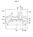
- FIG. 1 is a schematic diagram of an inspection system using a scanning electron microscope according to an embodiment of the invention
- FIG. 2 is an enlarged view of a scanning electron microscope chamber and a stage of an inspection system using a scanning electron microscope according to an embodiment of the invention
- FIG. 3 is a detailed view of a scanning electron microscope chamber of an inspection system using a scanning electron microscope according to an embodiment of the invention
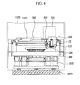
- FIG. 4 is a front view of an inspection system using a scanning electron microscope according to an embodiment of the invention.
- FIG. 5 is a rear view of an inspection system using a scanning electron microscope according to an embodiment of the invention.
- FIGS. 6A through 6C show an operational flow chart of an inspection system according to the practice of the present invention.
- an inspection system using a scanning electron microscope includes a scanning electron microscope chamber 100 scanning and irradiating an electron beam 1 onto an object to be inspected 10 to inspect the object to be inspected 10, a stage 200 separated from and disposed below the scanning electron microscope chamber 100 and mounting the object to be inspected 10, and a transverse guide 300 for transferring the scanning electron microscope chamber 100 on the stage 200.
- the object to be inspected 10 may be a flat panel display device such as a liquid crystal display (LCD) device and an organic light emitting diode (OLED) display device.
- LCD liquid crystal display
- OLED organic light emitting diode
- the scanning electron microscope chamber 100 includes a vacuum chamber 110 maintaining a vacuum condition, a scanning electron microscope 120 positioned inside the vacuum chamber 110 and scanning and irradiating the electron beam 1 onto the object to be inspected 10, and a signal detector 130 positioned inside the vacuum chamber 110 and detecting a signal generated in the object to be inspected 10. As described, the scanning electron microscope 120 and the signal detector 130 are maintained under the vacuum condition inside the scanning electron microscope chamber 100.
- the scanning electron microscope 120 includes an electron gun 121 emitting the electron beam 1, an electromagnetic lens 122 such as a condenser lens and an objective lens controlling a propagating direction of the electron beam 1, and an aperture 123 controlling an amount of the propagating electron beam 1.
- an electromagnetic lens 122 such as a condenser lens and an objective lens controlling a propagating direction of the electron beam 1
- an aperture 123 controlling an amount of the propagating electron beam 1.
- the signal detector 130 includes a secondary electron detector 131 detecting secondary electrons (SE) generated in the object to be inspected 10 by the electron beam 1 scanned and irradiated onto the object to be inspected 10, a back-scattering electron detector 132 detecting back-scattering electrons (BSE) generated in the object to be inspected 10, and a characteristic X-ray detector 133 detecting a characteristic X-ray generated in the object to be inspected 10.
- SE secondary electrons
- BSE back-scattering electrons
- the secondary electron detector 131 and the back-scattering electron detector 132 are attached below the scanning electron microscope 120, and the characteristic X-ray detector 133 is obliquely installed to the side surface of the scanning electron microscope 120.
- the characteristic X-ray detector 133 detects the object to be inspected 10 positioned in the atmospheric condition and the characteristic X-ray generated by the reaction of the electron beam 1 to analyze the components of the object to be inspected 10.
- an angle of the characteristic X-ray detector 133 may be controlled or the characteristic X-ray detector 133 may be carried in the scanning electron microscope chamber 100.
- an angle controller 134 is installed on the characteristic X-ray detector 133 and a characteristic X-ray detector carry-out door 111 is installed in the scanning electron microscope chamber 100.
- a membrane 140 is installed on a lower portion 145 of the scanning electron microscope chamber 100 to seal an opening 155 constructed in the lower portion 145.
- the membrane 140 may be formed of a non-conductive material including carbon (C), nitrogen (N), oxygen (O), or silicon (Si) and a material having transmittance and low absorption such that the electron beam 1, the secondary electrons, the back-scattering electrons, and the characteristic X-ray are not absorbed by the membrane 140 and are transmitted through the membrane 140.
- the thickness may be in a range of 10 nm to 3 ⁇ m, and in this case, the transmittance of the membrane 140 is in a range of 90 % to 100 %.
- the thickness of the membrane 140 is less than 10 nm, the membrane 140 is so thin that the membrane 140 may be easily damaged by a physical impact; when the thickness of the membrane 140 is more than 3 ⁇ m, the transmittance is less than 90 % such that the electron beam 1 may be partially absorbed by the membrane 140 and thereby correct inspection may not be performed.
- This membrane 140 maintains the vacuum condition of the scanning electron microscope chamber 100, and the electron beam 1 scanned in the scanning electron microscope 120 is simultaneously passed through the membrane 140 and may be irradiated onto the object to be inspected 10. Also, detecting signals of the secondary electrons, the back-scattering electrons, and the characteristic X-ray generated in the object to be inspected 10 are sent back to the interior of the scanning electron microscope chamber 100 such that they are transmitted to the secondary electron detector 131, the back-scattering electron detector 132, and the characteristic X-ray detector 133. Therefore, the membrane 140 maintains the atmospheric conditions between a space d between the scanning electron microscope chamber 100 and the object to be inspected 10.
- a contemporary vacuum scanning electron microscope 120 is limited to the size of the vacuum chamber 110 such that inspection of an object to be inspected 10 of a larger size such as a flat panel display device is difficult; according to the present invention, however, the atmospheric conditions are maintained between the scanning electron microscope chamber 100 and the object to be inspected 10 such that the inspection of the object to be inspected 10 of a larger size becomes possible in the atmospheric conditions. Therefore, the shape, the component, the structure, etc., of the object to be inspected 10 of a larger size may be observed and analyzed.
- the object to be inspected 10 with a larger size may be inspected for the analysis without damage to the object to be inspected 10 of a larger size such that the inspection cost may be reduced and the yield of manufacturing of the object to be inspected 10 may be improved.
- the object to be inspected 10 is positioned in the atmospheric conditions such that image distortion of the object to be inspected 10 caused by the charging effect generated in the vacuum chamber 110 is prevented and the object to be inspected 10 is not contaminated by carbon, thereby realizing the correct inspection.
- an optical microscope 400 is attached to the scanning electron microscope chamber 100, and irradiates light to the object to be inspected 10 to inspect the existence of a particle 2 attached to the surface of the object to be inspected 10.
- the optical microscope 400 may be attached to the scanning electron microscope chamber 100 such that the optical microscope 400 may be simultaneously moved with the scanning electron microscope chamber 100 by the transverse guide 300.
- a possible magnification of the optical microscope 400 is about 100 times at a maximum, and a possible magnification in the scanning electron microscope chamber 100 is about a million times such that the resolution of the scanning electron microscope chamber 100 is possible to be several nanometers. Accordingly, a first optical inspection of the object to be inspected 10 may be performed through the optical microscope 400, and a second detailed inspection of the object to be inspected 10 may be performed through the scanning electron microscope chamber 100 to obtain the information for the shape, the size, and the component of the particle 2.
- the inspection system using the scanning electron microscope includes the scanning electron microscope chamber 100 and the optical microscope 400 connected thereto such that the optical image of the particle 2 generated from the object to be inspected 10, the 3-D information of the object to be inspected 10, and the component analysis may be performed simultaneously.
- the stage 200 may be moved in X-axis, Y-axis, and Z-axis directions to inspect the entire region of the object to be inspected 10, and the transverse guide 300 may also independently move the scanning electron microscope chamber 100 in the X-axis, Y-axis, and Z-axis directions to enable the performance of an inspection of the entire region of the object to be inspected 10. More specifically, the transverse guide 300 may have one or more guide rails 1200. The scanning electron microscope chamber 100 may move back and forth along the axial direction of the guide rails 1200 under the control of the transverse guide 300.
- the stage 200 is installed with a lift pin 210 to receive the object to be inspected 10 from a transferring robot.
- the scanning electron microscope chamber 100 and the optical microscope 400 attached thereto are connected to the transverse guide 300 such that the scanning electron microscope 120 and the optical microscope 400 may be simultaneously moved to a predetermined position over the object to be inspected 10 such that it is not limited to the size of the object to be inspected 10.
- the stage 200 is installed with a flatness device 500 controlling flatness of the stage 200.
- a plurality of flatness devices 500 may be installed to the stage 200.
- the flatness device 500 measures the flatness of the stage 200 and controls the flatness such that a physical collision between the scanning electron microscope chamber 100 and the object to be inspected 10 is prevented.
- the scanning electron microscope chamber 100 is attached with an interval control device 600, and the interval control device 600 measures the distance d between the scanning electron microscope chamber 100 and the object to be inspected 10 in real-time by using a laser sensor, and feeds a signal back to the transverse guide 300 to control the position of the scanning electron microscope chamber 100, and thereby the physical collision between the scanning electron microscope chamber 100 and the object to be inspected 10 is prevented.
- the distance d between the lower portion 145 of the scanning electron microscope chamber 100 and the object to be inspected 10 may be close to a millimeter degree; the inspection system using the scanning electron microscope according to an embodiment of the present invention may reduce the distance d between the membrane 140 of the scanning electron microscope chamber 100 and the object to be inspected 10 down to the micrometer degree by using the flatness device 500 and the interval control device 600 such that analysis ability of the object to be inspected 10 may be improved.
- the transverse guide 300 is installed together with the scanning electron microscope chamber 100, the optical microscope 400, and the interval control device 600 such that the scanning electron microscope chamber 100, the optical microscope 400, and the interval control device 600 may be integrally moved by the transverse guide 300. Accordingly, the scanning electron microscope chamber 100, the optical microscope 400, and the interval control device 600 are simultaneously moved to all inspection positions of the object to be inspected 10 by using the transverse guide 300 without the limitation of the size of the object to be inspected 10, thereby performing the inspection process.
- An electron control device 700 is installed on the transverse guide 300 to control the electronic devices disposed inside the scanning electron microscope chamber 100.
- a supporting plate 800 is installed to support the stage 200 and the transverse guide 300, and a membrane particle inspection and removing device 900 is installed on the supporting plate 800.
- the membrane particle inspection and removing device 900 performs the inspection and removal of the particle attached to the surface of the membrane 140 before the inspection of the object to be inspected 10 using the scanning electron microscope chamber 100. Accordingly, an incomplete inspection of the object to be inspected 10 caused by the existence of particles attached to the surface of the membrane 140 may be prevented.
- a vibration control device 1000 is installed under the supporting plate 800.
- the vibration control device 1000 measures and controls an external vibration, for example, the external vibration from a platform 2000 (as shown in FIG. 5 ) on which the inspection system is mounted; therefore, an influence by the external vibration on the scanning electron microscope chamber 100 may be prevented by the vibration control device 1000.
- the microscope chamber 100 is influenced by the external vibration; however in an embodiment of the present invention, the influence of the external vibration on the scanning electron microscope chamber 100 may be minimized in the atmospheric conditions by installing the vibration control device 1000.
- a cover frame 1100 is installed to entirely enclose the scanning electron microscope chamber 100, the stage 200, and the transverse guide 300.
- the cover frame 1100 is formed of a blocking material such as aluminum (Al) or permalloy such that external magnetism and noise generated by a surrounding device or a surrounding wire are prevented from being transmitted to the scanning electron microscope chamber 100. Therefore, the external magnetism and the external noise do not affect the scanning electron microscope chamber 100.
- the cover frame 1100 installed with a cover door 1110 for passing the object to be inspected 10 through and allow the object to be inspected 10 to be loaded to and unloaded from the stage 200. As described, during the inspection process for the object to be inspected 10, the cover door 1110 is closed such that the scanning electron microscope chamber 100 is completely shielded from the external magnetism and noise.
- a magnetic sensor 1120 is installed inside the cover frame 1100 to detect the magnetism on the scanning electron microscope 120.
- the detected magnitude of the magnetism by the magnetic sensor 1120 may be used as a feedback control signal to minimize the influence of the magnetism on the scanning electron microscope 120. Accordingly, the analysis ability for the object to be inspected 10 of the scanning electron microscope chamber 100 may be improved.
- the flatness device 500 and the variation control device 1000 are installed to the inspection system in the atmospheric conditions to inspect the object to be inspected 10 such that the influence of the external noise on the inspection system may be minimized.
- FIGS. 6A through 6C show an operational flow chart of an inspection system according to the practice of the present invention.
- the operation of the inspection system need not be limited to FIGS. 6A through 6C .
- the operation of the inspection system shown in FIGS. 6A through 6C may allow the inspection system to consecutively inspect a plurality of spots on an object.
- the operation of the inspection system may also allow the inspection system to continuously inspect a serial stream of a plurality of geometrically similar objects.
- the operation of the inspection system may include 10 sequential steps, steps S1 through S10, and 5 discrete steps, steps S110 through S150.
- a discrete step may be performed in parallel with at least one of the sequential steps.
- a discrete step may be performed simultaneously while another discrete step is being conducted.
- a discrete step may be performed before or after one of the sequential steps.
- step S1 the inspection system is initialized.
- the initialization may include moving scanning electron microscope chamber 100 to an initial position according to an initial position preprogrammed in transverse guide 300.
- the initialization may also include centering stage 200 to an initial position.
- the initialization may further include checking whether an object has been left on stage 200. If an object is found on stage 200, the object will be unloaded by a transfer robot or by an operator.
- step S1 completes, scanning electron microscope chamber 100 and stage 200 are spaced apart from each other to allow an object to be inspected to be loaded onto stage 200.
- the inspection system may first check the status of the cover door 1110 of the cover frame 1100. If the cover door 1100 is closed, the inspection system will open the cover door 1100. After that, the transfer robot or the operator loads an object 10 that will be inspected by the inspection system onto stage 200. If the cover door 1110 is already open, the transfer robot may directly load an object 10 onto stage 200. Once object 10 is loaded, the inspection system will close the cover door 1100.
- transverse guide 300 moves scanning electron microscope chamber 100 to a position above object 10.
- object 10 may be moved by stage 200 to a position below scanning electron microscope chamber 100.
- scanning electron microscope chamber 100 and object 10 may be simultaneously moved, each driven by transverse guide 300 and stage 200, respectively.
- step S3 scanning electron microscope chamber 100 is located at a first inspection position in accordance with object 10 from which a series of inspections of object 10 start. The operator may preprogram the first inspection position into transverse guide 300 and/or stage 200 prior to inspection. On the other hand, the operator may manually control transverse guide 300 and/or stage 200 to setup the first inspection position during step S3.
- transverse guide 300 may gradually lower or lift electron microscope chamber 100 toward, or away from, the planar surface of stage 200, so that scanning electron microscope chamber 100 and object 10 may have a first predetermined distance from each other from which optical microscope 400 may perform a first optical inspection.
- stage 200 may gradually lift or lower object 10 toward, or away from, the bottom surface of scanning electron microscope chamber 100, so that scanning electron microscope chamber 100 and object 10 may have the first predetermined distance from each other.
- scanning electron microscope chamber 100 and object 10 may simultaneously be moved toward, or away from, each other, driven by transverse guide 300 and stage 200, respectively, so that scanning electron microscope chamber 100 and object 10 may have the first predetermined distance from each other.
- optical microscope 400 will perform an optical inspection of object 10. If an optical inspection is not required, step S4 may be skipped.
- step S5 if an inspection through scanning electron microscope chamber 100 is required, after similar operations as described in step S4, scanning electron microscope chamber 100 and object 10 may have a second predetermined distance from each other from which scanning electron microscope chamber 100 may perform an inspection. Once the second predetermined distance between scanning electron microscope chamber 100 and object 10 is achieved, scanning electron microscope chamber 100 will perform a more detailed inspection of object 10. If an inspection through scanning electron microscope chamber 100 is not required, step S5 may be skipped. Accordingly, the second predetermined distance may be different from the first predetermined distance. On the other hand, second predetermined distance may be substantially equal to the first predetermined distance, if scanning electron microscope chamber 100 and optical microscope have been installed in certain positions. In this case, distance adjustment in step S5 may be not required and the first optical inspection and the second and more detailed inspection may be simultaneously carried out.
- step S6 if step S4 is skipped and an optical inspection is required according to the inspection results obtained in S5, similar operations as described in S4 may take place to perform an optical inspection. In this scenario, an optical inspection is preformed after an inspection through scanning electron microscope chamber 100.
- step S7 after the inspections at the first inspection position is completed, the inspection system will check whether the current distance between scanning electron microscope chamber 100 and object 10 is in a safe range for a direct lateral movement between scanning electron microscope chamber 100 and object 10. If the current distance is out of the safe range, transverse guide 300 will lift scanning electron microscope chamber 100, and/or stage 200 will lower object 10, until the distance is in the safe range. And then, transverse guide 300 repositions scanning electron microscope chamber 100, and/or stage 200 repositions object 10, until scanning electron microscope chamber 100 is repositioned to a new inspection position in accordance with object 10. The operator may preprogram the next inspection position into transverse guide 300 and/or stage 200 prior to inspection. On the other hand, the operator may manually control transverse guide 300 and/or stage 200 to setup the next inspection position during step S7. Detailed repositioning of scanning electron microscope chamber 100 and/or object 10 is similar to the operation as described in step S3.
- step S8 The inspection system repeats steps S4 through S7 to complete a series of inspections of object 10 currently borne by stage 200.
- transverse guide 300 moves scanning electron microscope chamber 100 to its initial position, stage 200 centers itself to its initial position, the inspection system opens the cover door 1110, and the transfer robot or the operator unloads the inspected object 10.
- step S10 the inspection system repeats steps S2 through S9 to initiate an inspection of another object from among a plurality of objects that await inspection. If necessary, the inspection system may perform step S1 prior to step S2.
- the inspection system is in idle state waiting for new inspections.
- step S110 interval control device 600 measures the distance between scanning electron microscope chamber 100 and object 10.
- the measured distance is sent to transverse guide 300 to control the position of scanning electron microscope chamber 100, and thereby a physical collision between scanning electron microscope chamber 100 and object 10 may be prevented.
- the measured distance may be sent to stage 200 to control the position of object 10.
- step S110 may be simultaneously carried out during or before each, or in response to any relative movement between scanning electron microscope chamber 100 and object 10.
- step S110 may be simultaneously carried out during or before an inspection of each of a plurality of objects.
- step S110 may be performed when the inspection system is in operation.
- step S120 magnetic sensor 1120 is employed to detect the presence of magnetism.
- the detected magnitude of the magnetism may be used as a feedback control signal in order to compensate for and to thereby minimized the influence of the magnetism on the scanning electron microscope 120.
- step S120 may be simultaneously carried out during an inspection or before an inspection.
- vibration control device 100 may measure and control external vibration in order to minimize the influence of the external noise on the inspection system.
- step S130 may be simultaneously performed during an inspection or before an inspection.
- step S140 membrane particle inspection and removing device 900 may check whether the exterior surface of membrane 140 contains any particles. If particles are found on the membrane 140, membrane particle inspection and removing device 900 will remove the particles. Preferably, step S140 may be carried out prior to step S6. Alternatively, step S140 may be conducted in other steps, such as step S1.
- flatness device 500 may measure the flatness of stage 200 and further control the flatness of stage 200.
- Step S150 is preferably performed prior to loading object 10.
- Step S150 may be included in step S1.
- steps S1 through S10 are sequentially conducted according one embodiment of the present invention
- the inspection system may have other operation sequences which are not illustrated in FIG. 6 .
- the operation order of steps S5 and S4 may be reversed, and in this case, step S7 may be skipped.
- steps S4 and S5 or steps S5 and S6 may be simultaneously conducted, and step S7 or step S4 may be consequently skipped.
- the inspection system may respond to abnormal signals detected by monitor devices, such as magnetic sensor 1120, interval control device 600, membrane particle inspection and removing device 900, and flatness device 500, interrupting the ongoing operation and sending an alert signal to the operator.
- monitor devices such as magnetic sensor 1120, interval control device 600, membrane particle inspection and removing device 900, and flatness device 500, interrupting the ongoing operation and sending an alert signal to the operator.
Landscapes
- Chemical & Material Sciences (AREA)
- Analytical Chemistry (AREA)
- Physics & Mathematics (AREA)
- General Physics & Mathematics (AREA)
- Optics & Photonics (AREA)
- Analysing Materials By The Use Of Radiation (AREA)
Abstract
Description
- The present invention relates generally to an inspection system |for use with a scanning electron microscope, and more particularly, to an inspection system that uses a scanning electron microscope to perform inspections of an object under atmospheric conditions without limitation of the size of the object.
- In general, flat panel display devices such as liquid crystal display (LCD) devices and organic light emitting diode (OLED) display devices are formed by depositing a plurality of thin films and wires on a substrate. In order to inspect for the existence of imperfections such as impurities or particles on a thin film of a flat panel display device or for short circuits between the wires, an inspection system constructed with a scanning electron microscope (SEM) is used.
- A vacuum scanning electron microscope may be used in the inspection system. The size of a specimen to be observed by a contemporary SEM is limited by the size of a vacuum chamber of the SEM. A vacuum scanning electron microscope that is capable of observing a semiconductor wafer fabricated up to 30 inches in width has been developed; however, usage of the such a vacuum scanning electron microscope is difficult for purposes such as conducting an inspection of the flat panel display devices of the size from 730 mm × 920 mm to 2200 mm × 2500 mm due to the size limitations on the vacuum chamber of the SEM.
- When the size of the vacuum chamber is increased so as to be able to receive a flat panel display device, a charging effect causes a secondary electron (SE) or a back-scattering electron (BSE) to be generated at an object to be inspected in the vacuum chamber, so that observation of an image of the object becomes difficult, and carbon contamination by a hydrocarbon compound (HxCx) may be generated by a pump used for the vacuum chamber.
- The foregoing discussion of this information disclosed in this Background section is only for enhancement of an understanding of the background of the described technology and therefore it may contain information that does not form the prior art that is already known in this country to a person of ordinary skill in the art.
- Accordingly, it is an object to provide an improved inspection system. An embodiment of the present invention therefore sets out to provide an inspection system using a scanning electron microscope for performing an inspection of an object to be inspected under atmospheric conditions without limitation upon the size of the object to be inspected.
- According to one embodiment of the present invention, an inspection system may include a scanning electron microscope chamber able to make an inspection of an object by using an electron beam and maintain a vacuum condition within the chamber, a stage positioned below the scanning electron microscope chamber to be separated therefrom and mounted with the object to be inspected; and a transverse guide for transferring the scanning electron microscope chamber on the stage. Atmospheric conditions are maintained between the scanning electron microscope chamber and the object to be inspected.
- An optical microscope may be attached to the scanning electron microscope chamber and irradiate light toward the object to be inspected in order to inspect the object to be inspected.
- A first optical inspection of the object to be inspected may be performed through the optical microscope, and a second detailed inspection of the object to be inspected may be performed through the scanning electron microscope chamber.
- The scanning electron microscope chamber may include a vacuum chamber; a scanning electron microscope positioned inside the vacuum chamber to scan the electron beam to the object to be inspected. A signal detector is positioned inside the vacuum chamber to detect a detection signal generated in the object to be inspected.
- The signal detector may include a secondary electron detector detecting secondary electrons generated in the object to be inspected; a back-scattering electron detector detecting back-scattering electrons generated in the object to be inspected; and a characteristic X-ray detector detecting a characteristic X-ray generated in the object to be inspected.
- A membrane installed below the scanning electron microscope chamber may be further included, and the membrane may permit passage of the electron beam scanned in the scanning electron microscope such that the secondary electrons, the back-scattering electrons, and the characteristic X-ray generated in the object to be inspected may be transferred inside the scanning electron microscope chamber.
- A flatness device may be connected to the stage in order to control the flatness of the stage.
- An interval control device may be connected to the scanning electron microscope chamber and control a distance between the scanning electron microscope chamber and the object to be inspected.
- A membrane particle inspection and removing device may inspect particles attached to the membrane and remove those particles found during the inspection from the membrane.
- The membrane particle inspection and removing device may perform the particle inspection and the particle removal of the membrane before the inspection of the object to be inspected using the scanning electron microscope chamber.
- A supporting plate supporting the stage and the transverse guide may be further included, and the membrane particle inspection and removing device may be installed on the supporting plate.
- A vibration control device may be installed below the supporting plate and measure and eliminate an external vibration to prevent, or at least ameliorate any influence caused by the external vibration on the scanning electron microscope chamber.
- A cover frame may enclose the scanning electron microscope chamber, the stage, and the transverse guide and remove magnetism and noise to prevent the magnetism and the noise from affecting the scanning electron microscope chamber.
- The object to be inspected may be a flat panel display device.
- A thickness of the membrane may be in a range of 10 nm to 3 µm, and the membrane may be made of a non-electrically conductive material.
- According to the present invention, by using the inspection system including the scanning electron microscope chamber and the optical microscope connected thereto, the optical image of the particle of the object to be inspected, 3-D information, and component analysis may be simultaneously performed.
- Also, the scanning electron microscope chamber and the optical microscope connected thereto are installed on the transverse guide such that the scanning electron microscope chamber and the optical microscope may be moved to a predetermined position relative to the object to be inspected. In this case, the size of the object to be inspected is not a limit upon the capacity or upon the performance of the inspection system.
- Also, a contemporary vacuum scanning electron microscope is limited to the size of the vacuum chamber such that inspection of an object to be inspected of a larger size such as a flat panel display device is difficult. According to the present invention, however, the atmospheric conditions are maintained between the scanning electron microscope chamber and the object to be inspected object such that the inspection of the object to be inspected of a larger size is possible under the atmospheric conditions, and thereby the shape, the component, the structure, etc., of the object to be inspected of a larger size may be observed and analyzed.
- According to the present invention, the object to be inspected of a larger size may be inspected for the analysis without damage to the object to be inspected such that a cost reduction and a yield improvement may be realized.
- Also, the object to be inspected is positioned in the atmospheric conditions such that the image distortion of the object to be inspected by the charging effect generated in the vacuum chamber is prevented and the object to be inspected is not contaminated by carbon, thereby realizing the correct inspection.
- As described, according to the characteristic of the scanning electron microscope that is sensitive to external noise such as external vibration, magnetism, and noise, the flatness device and the variation control device are installed to the inspection system in the atmospheric conditions to inspect the object to be inspected such that the influence of the external noise on the inspection system may be minimized.
- At least some of the above and other features of the invention are set out in the claims.
-
FIG. 1 is a schematic diagram of an inspection system using a scanning electron microscope according to an embodiment of the invention; -
FIG. 2 is an enlarged view of a scanning electron microscope chamber and a stage of an inspection system using a scanning electron microscope according to an embodiment of the invention; -
FIG. 3 is a detailed view of a scanning electron microscope chamber of an inspection system using a scanning electron microscope according to an embodiment of the invention; -
FIG. 4 is a front view of an inspection system using a scanning electron microscope according to an embodiment of the invention; -
FIG. 5 is a rear view of an inspection system using a scanning electron microscope according to an embodiment of the invention; and -
FIGS. 6A through 6C show an operational flow chart of an inspection system according to the practice of the present invention. - The present invention will be described more fully hereinafter with reference to the accompanying drawings, in which embodiments of the invention are shown. As those skilled in the art would realize, the described embodiments may be modified in various different ways, all without departing from the scope of the present invention.
- Descriptions of parts not related to the present invention are omitted, and like reference numerals designate like elements throughout the specification.
- Thus, an inspection system using a scanning electron microscope according to an embodiment of the invention will be described with reference to
FIG. 1 to FIG. 5 . - As shown in
FIG. 1 to FIG. 5 , an inspection system using a scanning electron microscope according to an embodiment of the invention includes a scanningelectron microscope chamber 100 scanning and irradiating anelectron beam 1 onto an object to be inspected 10 to inspect the object to be inspected 10, astage 200 separated from and disposed below the scanningelectron microscope chamber 100 and mounting the object to be inspected 10, and atransverse guide 300 for transferring the scanningelectron microscope chamber 100 on thestage 200. The object to be inspected 10 may be a flat panel display device such as a liquid crystal display (LCD) device and an organic light emitting diode (OLED) display device. - As shown in
FIG. 2 , the scanningelectron microscope chamber 100 includes avacuum chamber 110 maintaining a vacuum condition, ascanning electron microscope 120 positioned inside thevacuum chamber 110 and scanning and irradiating theelectron beam 1 onto the object to be inspected 10, and asignal detector 130 positioned inside thevacuum chamber 110 and detecting a signal generated in the object to be inspected 10. As described, thescanning electron microscope 120 and thesignal detector 130 are maintained under the vacuum condition inside the scanningelectron microscope chamber 100. - The
scanning electron microscope 120 includes anelectron gun 121 emitting theelectron beam 1, anelectromagnetic lens 122 such as a condenser lens and an objective lens controlling a propagating direction of theelectron beam 1, and anaperture 123 controlling an amount of the propagatingelectron beam 1. - The
signal detector 130 includes asecondary electron detector 131 detecting secondary electrons (SE) generated in the object to be inspected 10 by theelectron beam 1 scanned and irradiated onto the object to be inspected 10, a back-scatteringelectron detector 132 detecting back-scattering electrons (BSE) generated in the object to be inspected 10, and acharacteristic X-ray detector 133 detecting a characteristic X-ray generated in the object to be inspected 10. The image of the object to be inspected 10 and components thereof may be measured and analyzed by using thesignal detector 130. - The
secondary electron detector 131 and the back-scattering electron detector 132 are attached below thescanning electron microscope 120, and thecharacteristic X-ray detector 133 is obliquely installed to the side surface of thescanning electron microscope 120. Thecharacteristic X-ray detector 133 detects the object to be inspected 10 positioned in the atmospheric condition and the characteristic X-ray generated by the reaction of theelectron beam 1 to analyze the components of the object to be inspected 10. To minimize an influence of thecharacteristic X-ray detector 133 on thescanning electron microscope 120, an angle of thecharacteristic X-ray detector 133 may be controlled or thecharacteristic X-ray detector 133 may be carried in the scanningelectron microscope chamber 100. For this, an angle controller 134 is installed on thecharacteristic X-ray detector 133 and a characteristic X-ray detector carry-outdoor 111 is installed in the scanningelectron microscope chamber 100. - As shown in
FIG. 2 , amembrane 140 is installed on alower portion 145 of the scanningelectron microscope chamber 100 to seal anopening 155 constructed in thelower portion 145. Themembrane 140 may be formed of a non-conductive material including carbon (C), nitrogen (N), oxygen (O), or silicon (Si) and a material having transmittance and low absorption such that theelectron beam 1, the secondary electrons, the back-scattering electrons, and the characteristic X-ray are not absorbed by themembrane 140 and are transmitted through themembrane 140. In themembrane 140 made of carbon (C) and having excellent transmittance, the thickness may be in a range of 10 nm to 3 µm, and in this case, the transmittance of themembrane 140 is in a range of 90 % to 100 %. When the thickness of themembrane 140 is less than 10 nm, themembrane 140 is so thin that themembrane 140 may be easily damaged by a physical impact; when the thickness of themembrane 140 is more than 3 µm, the transmittance is less than 90 % such that theelectron beam 1 may be partially absorbed by themembrane 140 and thereby correct inspection may not be performed. - This
membrane 140 maintains the vacuum condition of the scanningelectron microscope chamber 100, and theelectron beam 1 scanned in thescanning electron microscope 120 is simultaneously passed through themembrane 140 and may be irradiated onto the object to be inspected 10. Also, detecting signals of the secondary electrons, the back-scattering electrons, and the characteristic X-ray generated in the object to be inspected 10 are sent back to the interior of the scanningelectron microscope chamber 100 such that they are transmitted to thesecondary electron detector 131, the back-scattering electron detector 132, and thecharacteristic X-ray detector 133. Therefore, themembrane 140 maintains the atmospheric conditions between a space d between the scanningelectron microscope chamber 100 and the object to be inspected 10. Accordingly, a contemporary vacuumscanning electron microscope 120 is limited to the size of thevacuum chamber 110 such that inspection of an object to be inspected 10 of a larger size such as a flat panel display device is difficult; according to the present invention, however, the atmospheric conditions are maintained between the scanningelectron microscope chamber 100 and the object to be inspected 10 such that the inspection of the object to be inspected 10 of a larger size becomes possible in the atmospheric conditions. Therefore, the shape, the component, the structure, etc., of the object to be inspected 10 of a larger size may be observed and analyzed. - Accordingly, the object to be inspected 10 with a larger size may be inspected for the analysis without damage to the object to be inspected 10 of a larger size such that the inspection cost may be reduced and the yield of manufacturing of the object to be inspected 10 may be improved.
- Also, the object to be inspected 10 is positioned in the atmospheric conditions such that image distortion of the object to be inspected 10 caused by the charging effect generated in the
vacuum chamber 110 is prevented and the object to be inspected 10 is not contaminated by carbon, thereby realizing the correct inspection. - As shown in
FIG. 2 , anoptical microscope 400 is attached to the scanningelectron microscope chamber 100, and irradiates light to the object to be inspected 10 to inspect the existence of aparticle 2 attached to the surface of the object to be inspected 10. As described, theoptical microscope 400 may be attached to the scanningelectron microscope chamber 100 such that theoptical microscope 400 may be simultaneously moved with the scanningelectron microscope chamber 100 by thetransverse guide 300. - A possible magnification of the
optical microscope 400 is about 100 times at a maximum, and a possible magnification in the scanningelectron microscope chamber 100 is about a million times such that the resolution of the scanningelectron microscope chamber 100 is possible to be several nanometers. Accordingly, a first optical inspection of the object to be inspected 10 may be performed through theoptical microscope 400, and a second detailed inspection of the object to be inspected 10 may be performed through the scanningelectron microscope chamber 100 to obtain the information for the shape, the size, and the component of theparticle 2. - As described, the inspection system using the scanning electron microscope according to this embodiment of the present invention includes the scanning
electron microscope chamber 100 and theoptical microscope 400 connected thereto such that the optical image of theparticle 2 generated from the object to be inspected 10, the 3-D information of the object to be inspected 10, and the component analysis may be performed simultaneously. - As shown in
FIG. 1 , thestage 200 may be moved in X-axis, Y-axis, and Z-axis directions to inspect the entire region of the object to be inspected 10, and thetransverse guide 300 may also independently move the scanningelectron microscope chamber 100 in the X-axis, Y-axis, and Z-axis directions to enable the performance of an inspection of the entire region of the object to be inspected 10. More specifically, thetransverse guide 300 may have one ormore guide rails 1200. The scanningelectron microscope chamber 100 may move back and forth along the axial direction of theguide rails 1200 under the control of thetransverse guide 300. Thestage 200 is installed with alift pin 210 to receive the object to be inspected 10 from a transferring robot. - The scanning
electron microscope chamber 100 and theoptical microscope 400 attached thereto are connected to thetransverse guide 300 such that thescanning electron microscope 120 and theoptical microscope 400 may be simultaneously moved to a predetermined position over the object to be inspected 10 such that it is not limited to the size of the object to be inspected 10. - The
stage 200 is installed with aflatness device 500 controlling flatness of thestage 200. A plurality offlatness devices 500 may be installed to thestage 200. Theflatness device 500 measures the flatness of thestage 200 and controls the flatness such that a physical collision between the scanningelectron microscope chamber 100 and the object to be inspected 10 is prevented. - The scanning
electron microscope chamber 100 is attached with aninterval control device 600, and theinterval control device 600 measures the distance d between the scanningelectron microscope chamber 100 and the object to be inspected 10 in real-time by using a laser sensor, and feeds a signal back to thetransverse guide 300 to control the position of the scanningelectron microscope chamber 100, and thereby the physical collision between the scanningelectron microscope chamber 100 and the object to be inspected 10 is prevented. - The distance d between the
lower portion 145 of the scanningelectron microscope chamber 100 and the object to be inspected 10 may be close to a millimeter degree; the inspection system using the scanning electron microscope according to an embodiment of the present invention may reduce the distance d between themembrane 140 of the scanningelectron microscope chamber 100 and the object to be inspected 10 down to the micrometer degree by using theflatness device 500 and theinterval control device 600 such that analysis ability of the object to be inspected 10 may be improved. - As described, the
transverse guide 300 is installed together with the scanningelectron microscope chamber 100, theoptical microscope 400, and theinterval control device 600 such that the scanningelectron microscope chamber 100, theoptical microscope 400, and theinterval control device 600 may be integrally moved by thetransverse guide 300. Accordingly, the scanningelectron microscope chamber 100, theoptical microscope 400, and theinterval control device 600 are simultaneously moved to all inspection positions of the object to be inspected 10 by using thetransverse guide 300 without the limitation of the size of the object to be inspected 10, thereby performing the inspection process. - An
electron control device 700 is installed on thetransverse guide 300 to control the electronic devices disposed inside the scanningelectron microscope chamber 100. - A supporting
plate 800 is installed to support thestage 200 and thetransverse guide 300, and a membrane particle inspection and removingdevice 900 is installed on the supportingplate 800. The membrane particle inspection and removingdevice 900 performs the inspection and removal of the particle attached to the surface of themembrane 140 before the inspection of the object to be inspected 10 using the scanningelectron microscope chamber 100. Accordingly, an incomplete inspection of the object to be inspected 10 caused by the existence of particles attached to the surface of themembrane 140 may be prevented. - A
vibration control device 1000 is installed under the supportingplate 800. Thevibration control device 1000 measures and controls an external vibration, for example, the external vibration from a platform 2000 (as shown inFIG. 5 ) on which the inspection system is mounted; therefore, an influence by the external vibration on the scanningelectron microscope chamber 100 may be prevented by thevibration control device 1000. In the atmospheric conditions, themicroscope chamber 100 is influenced by the external vibration; however in an embodiment of the present invention, the influence of the external vibration on the scanningelectron microscope chamber 100 may be minimized in the atmospheric conditions by installing thevibration control device 1000. - A
cover frame 1100 is installed to entirely enclose the scanningelectron microscope chamber 100, thestage 200, and thetransverse guide 300. Thecover frame 1100 is formed of a blocking material such as aluminum (Al) or permalloy such that external magnetism and noise generated by a surrounding device or a surrounding wire are prevented from being transmitted to the scanningelectron microscope chamber 100. Therefore, the external magnetism and the external noise do not affect the scanningelectron microscope chamber 100. Thecover frame 1100 installed with acover door 1110 for passing the object to be inspected 10 through and allow the object to be inspected 10 to be loaded to and unloaded from thestage 200. As described, during the inspection process for the object to be inspected 10, thecover door 1110 is closed such that the scanningelectron microscope chamber 100 is completely shielded from the external magnetism and noise. - Also, a
magnetic sensor 1120 is installed inside thecover frame 1100 to detect the magnetism on thescanning electron microscope 120. The detected magnitude of the magnetism by themagnetic sensor 1120 may be used as a feedback control signal to minimize the influence of the magnetism on thescanning electron microscope 120. Accordingly, the analysis ability for the object to be inspected 10 of the scanningelectron microscope chamber 100 may be improved. - As described, according to the characteristics of the
scanning electron microscope 120 that is sensitive to external noise such as external vibration, magnetism, and noise, theflatness device 500 and thevariation control device 1000 are installed to the inspection system in the atmospheric conditions to inspect the object to be inspected 10 such that the influence of the external noise on the inspection system may be minimized. -
FIGS. 6A through 6C show an operational flow chart of an inspection system according to the practice of the present invention. The operation of the inspection system need not be limited toFIGS. 6A through 6C . - The operation of the inspection system shown in
FIGS. 6A through 6C may allow the inspection system to consecutively inspect a plurality of spots on an object. The operation of the inspection system may also allow the inspection system to continuously inspect a serial stream of a plurality of geometrically similar objects. - As shown in
FIG. 6A through 6C , the operation of the inspection system may include 10 sequential steps, steps S1 through S10, and 5 discrete steps, steps S110 through S150. A discrete step may be performed in parallel with at least one of the sequential steps. On the other hand, a discrete step may be performed simultaneously while another discrete step is being conducted. Alternatively, a discrete step may be performed before or after one of the sequential steps. Detailed operation of one process for the practice of the inspection system is described as follows. - In step S1, the inspection system is initialized. The initialization may include moving scanning
electron microscope chamber 100 to an initial position according to an initial position preprogrammed intransverse guide 300. The initialization may also include centeringstage 200 to an initial position. The initialization may further include checking whether an object has been left onstage 200. If an object is found onstage 200, the object will be unloaded by a transfer robot or by an operator. Once step S1 completes, scanningelectron microscope chamber 100 andstage 200 are spaced apart from each other to allow an object to be inspected to be loaded ontostage 200. - In step S2, the inspection system may first check the status of the
cover door 1110 of thecover frame 1100. If thecover door 1100 is closed, the inspection system will open thecover door 1100. After that, the transfer robot or the operator loads anobject 10 that will be inspected by the inspection system ontostage 200. If thecover door 1110 is already open, the transfer robot may directly load anobject 10 ontostage 200. Onceobject 10 is loaded, the inspection system will close thecover door 1100. - In step S3,
transverse guide 300 moves scanningelectron microscope chamber 100 to a position aboveobject 10. Alternatively, object 10 may be moved bystage 200 to a position below scanningelectron microscope chamber 100. Optionally, scanningelectron microscope chamber 100 and object 10 may be simultaneously moved, each driven bytransverse guide 300 andstage 200, respectively. Once step S3 completes, scanningelectron microscope chamber 100 is located at a first inspection position in accordance withobject 10 from which a series of inspections ofobject 10 start. The operator may preprogram the first inspection position intotransverse guide 300 and/orstage 200 prior to inspection. On the other hand, the operator may manually controltransverse guide 300 and/orstage 200 to setup the first inspection position during step S3. - In step S4, if an optical inspection is required,
transverse guide 300 may gradually lower or liftelectron microscope chamber 100 toward, or away from, the planar surface ofstage 200, so that scanningelectron microscope chamber 100 and object 10 may have a first predetermined distance from each other from whichoptical microscope 400 may perform a first optical inspection. Alternatively,stage 200 may gradually lift orlower object 10 toward, or away from, the bottom surface of scanningelectron microscope chamber 100, so that scanningelectron microscope chamber 100 and object 10 may have the first predetermined distance from each other. Optionally, scanningelectron microscope chamber 100 and object 10 may simultaneously be moved toward, or away from, each other, driven bytransverse guide 300 andstage 200, respectively, so that scanningelectron microscope chamber 100 and object 10 may have the first predetermined distance from each other. Once the first predetermined distance between scanningelectron microscope chamber 100 andobject 10 is achieved,optical microscope 400 will perform an optical inspection ofobject 10. If an optical inspection is not required, step S4 may be skipped. - In step S5, if an inspection through scanning
electron microscope chamber 100 is required, after similar operations as described in step S4, scanningelectron microscope chamber 100 and object 10 may have a second predetermined distance from each other from which scanningelectron microscope chamber 100 may perform an inspection. Once the second predetermined distance between scanningelectron microscope chamber 100 andobject 10 is achieved, scanningelectron microscope chamber 100 will perform a more detailed inspection ofobject 10. If an inspection through scanningelectron microscope chamber 100 is not required, step S5 may be skipped. Accordingly, the second predetermined distance may be different from the first predetermined distance. On the other hand, second predetermined distance may be substantially equal to the first predetermined distance, if scanningelectron microscope chamber 100 and optical microscope have been installed in certain positions. In this case, distance adjustment in step S5 may be not required and the first optical inspection and the second and more detailed inspection may be simultaneously carried out. - In step S6, if step S4 is skipped and an optical inspection is required according to the inspection results obtained in S5, similar operations as described in S4 may take place to perform an optical inspection. In this scenario, an optical inspection is preformed after an inspection through scanning
electron microscope chamber 100. - In step S7, after the inspections at the first inspection position is completed, the inspection system will check whether the current distance between scanning
electron microscope chamber 100 andobject 10 is in a safe range for a direct lateral movement between scanningelectron microscope chamber 100 andobject 10. If the current distance is out of the safe range,transverse guide 300 will lift scanningelectron microscope chamber 100, and/orstage 200 will lowerobject 10, until the distance is in the safe range. And then,transverse guide 300 repositions scanningelectron microscope chamber 100, and/orstage 200 repositionsobject 10, until scanningelectron microscope chamber 100 is repositioned to a new inspection position in accordance withobject 10. The operator may preprogram the next inspection position intotransverse guide 300 and/orstage 200 prior to inspection. On the other hand, the operator may manually controltransverse guide 300 and/orstage 200 to setup the next inspection position during step S7. Detailed repositioning of scanningelectron microscope chamber 100 and/orobject 10 is similar to the operation as described in step S3. - In step S8, The inspection system repeats steps S4 through S7 to complete a series of inspections of
object 10 currently borne bystage 200. - In step S9,
transverse guide 300 moves scanningelectron microscope chamber 100 to its initial position,stage 200 centers itself to its initial position, the inspection system opens thecover door 1110, and the transfer robot or the operator unloads the inspectedobject 10. - In step S10, the inspection system repeats steps S2 through S9 to initiate an inspection of another object from among a plurality of objects that await inspection. If necessary, the inspection system may perform step S1 prior to step S2.
- Once the entire inspection of all of the objects is complete, and the process of inspection ends. The inspection system is in idle state waiting for new inspections.
- In step S110,
interval control device 600 measures the distance between scanningelectron microscope chamber 100 andobject 10. The measured distance is sent totransverse guide 300 to control the position of scanningelectron microscope chamber 100, and thereby a physical collision between scanningelectron microscope chamber 100 and object 10 may be prevented. Alternatively, the measured distance may be sent to stage 200 to control the position ofobject 10. Preferably, step S110 may be simultaneously carried out during or before each, or in response to any relative movement between scanningelectron microscope chamber 100 andobject 10. Alternatively, step S110 may be simultaneously carried out during or before an inspection of each of a plurality of objects. Optionally, step S110 may be performed when the inspection system is in operation. - In step S120,
magnetic sensor 1120 is employed to detect the presence of magnetism. The detected magnitude of the magnetism may be used as a feedback control signal in order to compensate for and to thereby minimized the influence of the magnetism on thescanning electron microscope 120. Preferably, step S120 may be simultaneously carried out during an inspection or before an inspection. - In step S130,
vibration control device 100 may measure and control external vibration in order to minimize the influence of the external noise on the inspection system. Preferably, step S130 may be simultaneously performed during an inspection or before an inspection. - In step S140, membrane particle inspection and removing
device 900 may check whether the exterior surface ofmembrane 140 contains any particles. If particles are found on themembrane 140, membrane particle inspection and removingdevice 900 will remove the particles. Preferably, step S140 may be carried out prior to step S6. Alternatively, step S140 may be conducted in other steps, such as step S1. - In step S150,
flatness device 500 may measure the flatness ofstage 200 and further control the flatness ofstage 200. Step S150 is preferably performed prior to loadingobject 10. Alternatively, Step S150 may be included in step S1. - Although as shown in
FIG. 6A and6B , steps S1 through S10 are sequentially conducted according one embodiment of the present invention, the inspection system may have other operation sequences which are not illustrated inFIG. 6 . For example, the operation order of steps S5 and S4 may be reversed, and in this case, step S7 may be skipped. For another example, if the first distance to perform an optical inspection is substantially equal to the second distance to perform a more detailed inspection through scanningelectron microscope chamber 100, steps S4 and S5 or steps S5 and S6 may be simultaneously conducted, and step S7 or step S4 may be consequently skipped. According to other embodiments of the present invention, the inspection system may respond to abnormal signals detected by monitor devices, such asmagnetic sensor 1120,interval control device 600, membrane particle inspection and removingdevice 900, andflatness device 500, interrupting the ongoing operation and sending an alert signal to the operator. - While the invention has been described in connection with what are presently considered to be practical embodiments, it is to be understood that the invention is not limited to the disclosed embodiments, but, on the contrary, is intended to cover various modifications and equivalent arrangements included within the scope of the appended claims.
Claims (17)
- An inspection system for a scanning electron microscope, the inspection system comprising:a scanning electron microscope chamber disposed to accommodate an inspection of an object by an electron beam and maintain a vacuum condition within the chamber;a stage positioned below the scanning electron microscope chamber to support the object to be inspected, the stage being spaced apart from the scanning electron microscope chamber;a transverse guide disposed to transfer the scanning electron microscope chamber on the stage; anda space disposed to maintain a space in atmospheric conditions between the scanning electron microscope chamber and the object.
- An inspection system according to claim 1, further comprising an optical microscope attached to the scanning electron microscope chamber with a disposition to perform the inspection of the object by irradiating light onto the object.
- An inspection system according to claim 2, adapted to enable a first optical inspection of the object to be performed through the optical microscope, and a second and more detailed inspection of the object to be performed through the scanning electron microscope chamber.
- An inspection system according claim 2 or 3, wherein
the scanning electron microscope chamber comprises: a vacuum chamber;
the scanning electron microscope positioned inside the vacuum chamber and arranged for scanning the electron beam toward the object to be inspected; and
a signal detector positioned inside the vacuum chamber for detecting a signal generated in the object to be inspected. - An inspection system according to claim 4, wherein the signal detector comprises: a secondary electron detector sensitive to secondary electrons generated in the object to be inspected;
a back-scattering electron detector sensitive to back-scattering electrons generated in the object to be inspected; and
a characteristic X-ray detector sensitive to a characteristic X-ray generated in the object to be inspected. - An inspection system according to claim 5, further comprising:a membrane installed on a lower portion of the scanning electron microscope chamber for facing the object;the membrane being adapted to pass the electron beam scanned by the scanning electron microscope to permit transfer of the secondary electrons, the back-scattering electrons, and the characteristic X-ray generated in the object to be inspected to the interior of the scanning electron microscope chamber.
- An inspection system according to any preceding claim, further comprising a flatness device connected to the stage for controlling flatness of the stage.
- An inspection system according to any preceding claim, further comprising an interval control device connected to the scanning electron microscope chamber for controlling a distance between the scanning electron microscope chamber and the object to be inspected.
- An inspection system according to claim 6 or any claim dependent thereon, further comprising a membrane particle inspection and removing device disposed to inspect a particle disposed on the membrane and adapted to remove the particle from the membrane.
- An inspection system according to claim 9, wherein the membrane particle inspection and removing device is adapted to inspect the particle and remove the particle prior to the object being inspected.
- An inspection system according to claim 10, further comprising a supporting plate supporting the stage and the transverse guide, the membrane particle inspection and removing device being installed on the supporting plate.
- An inspection system according to claim 11, further comprising a vibration control device installed below the supporting plate, the vibration control device being adapted to measured and eliminate an external vibration in order to prevent influence by the external vibration on the scanning electron microscope chamber.
- An inspection system according to any preceding claim, further comprising a cover frame enclosing the scanning electron microscope chamber, the stage, and the transverse guide; the cover frame being adapted to discourage magnetism and noise from affecting the scanning electron microscope chamber by attenuating the magnetism and noise.
- An inspection system according to any preceding claim, wherein the stage is adapted to support a flat panel display device as the object to be inspected.
- An inspection system according to claim 6 or any claim dependent thereon, wherein a thickness of the membrane is in a range of 10 nm to 3 µm.
- An inspection system according to claim 15, wherein the membrane comprises an electrically non-conductive material.
- A scanning electron microscope system comprising an inspection system according to any preceding claim and a scanning electron microscope situated inside the scanning electron microscope chamber.
Applications Claiming Priority (1)
| Application Number | Priority Date | Filing Date | Title |
|---|---|---|---|
| KR1020120057468A KR101914231B1 (en) | 2012-05-30 | 2012-05-30 | Inspection system using scanning electron microscope |
Publications (2)
| Publication Number | Publication Date |
|---|---|
| EP2669927A2 true EP2669927A2 (en) | 2013-12-04 |
| EP2669927A3 EP2669927A3 (en) | 2015-08-12 |
Family
ID=48520797
Family Applications (1)
| Application Number | Title | Priority Date | Filing Date |
|---|---|---|---|
| EP13169847.4A Ceased EP2669927A3 (en) | 2012-05-30 | 2013-05-30 | Inspection system for use with scanning electron microscope |
Country Status (6)
| Country | Link |
|---|---|
| US (1) | US8890067B2 (en) |
| EP (1) | EP2669927A3 (en) |
| JP (1) | JP6288951B2 (en) |
| KR (1) | KR101914231B1 (en) |
| CN (1) | CN103454295B (en) |
| TW (1) | TWI597757B (en) |
Cited By (1)
| Publication number | Priority date | Publication date | Assignee | Title |
|---|---|---|---|---|
| CN112669397A (en) * | 2019-10-16 | 2021-04-16 | 卡尔蔡司有限公司 | Optical three-dimensional scanning for collision avoidance in microscopy systems |
Families Citing this family (32)
| Publication number | Priority date | Publication date | Assignee | Title |
|---|---|---|---|---|
| US10197501B2 (en) | 2011-12-12 | 2019-02-05 | Kla-Tencor Corporation | Electron-bombarded charge-coupled device and inspection systems using EBCCD detectors |
| US9496425B2 (en) | 2012-04-10 | 2016-11-15 | Kla-Tencor Corporation | Back-illuminated sensor with boron layer |
| US9601299B2 (en) | 2012-08-03 | 2017-03-21 | Kla-Tencor Corporation | Photocathode including silicon substrate with boron layer |
| US9426400B2 (en) | 2012-12-10 | 2016-08-23 | Kla-Tencor Corporation | Method and apparatus for high speed acquisition of moving images using pulsed illumination |
| CN104006949A (en) * | 2013-02-26 | 2014-08-27 | 北京京东方光电科技有限公司 | Transmittance detection device |
| KR102026936B1 (en) * | 2013-03-26 | 2019-10-01 | 삼성디스플레이 주식회사 | Inspection system using scanning electron microscope |
| US9478402B2 (en) | 2013-04-01 | 2016-10-25 | Kla-Tencor Corporation | Photomultiplier tube, image sensor, and an inspection system using a PMT or image sensor |
| US9347890B2 (en) | 2013-12-19 | 2016-05-24 | Kla-Tencor Corporation | Low-noise sensor and an inspection system using a low-noise sensor |
| US9748294B2 (en) | 2014-01-10 | 2017-08-29 | Hamamatsu Photonics K.K. | Anti-reflection layer for back-illuminated sensor |
| KR20150107939A (en) * | 2014-03-13 | 2015-09-24 | 참엔지니어링(주) | Apparatus for observating specimen |
| US9410901B2 (en) | 2014-03-17 | 2016-08-09 | Kla-Tencor Corporation | Image sensor, an inspection system and a method of inspecting an article |
| US9767986B2 (en) * | 2014-08-29 | 2017-09-19 | Kla-Tencor Corporation | Scanning electron microscope and methods of inspecting and reviewing samples |
| TWI573165B (en) * | 2014-12-09 | 2017-03-01 | 財團法人工業技術研究院 | Electron microscope, reader and acquiring elemental spectrum method |
| US9860466B2 (en) | 2015-05-14 | 2018-01-02 | Kla-Tencor Corporation | Sensor with electrically controllable aperture for inspection and metrology systems |
| US10748730B2 (en) | 2015-05-21 | 2020-08-18 | Kla-Tencor Corporation | Photocathode including field emitter array on a silicon substrate with boron layer |
| US10462391B2 (en) | 2015-08-14 | 2019-10-29 | Kla-Tencor Corporation | Dark-field inspection using a low-noise sensor |
| JP6880032B2 (en) * | 2015-12-24 | 2021-06-02 | エーエスエムエル ネザーランズ ビー.ブイ. | Methods and equipment for inspection |
| US10313622B2 (en) | 2016-04-06 | 2019-06-04 | Kla-Tencor Corporation | Dual-column-parallel CCD sensor and inspection systems using a sensor |
| US10778925B2 (en) | 2016-04-06 | 2020-09-15 | Kla-Tencor Corporation | Multiple column per channel CCD sensor architecture for inspection and metrology |
| JP6797907B2 (en) * | 2016-05-10 | 2020-12-09 | 株式会社住化分析センター | Inspection and analysis methods for organic electronic devices, and their use |
| CN106291899A (en) * | 2016-09-29 | 2017-01-04 | 东方晶源微电子科技(北京)有限公司 | Lighting module, optical microscope system and Electron-beam measuring device |
| CN106770405A (en) * | 2016-12-09 | 2017-05-31 | 清华大学 | Ultraphotic diffraction imaging device under a kind of complete atmospheric pressure |
| CN107116308B (en) * | 2017-05-03 | 2019-01-04 | 湖北工业大学 | Waveguide micro/nano processing system and processing method |
| US10049904B1 (en) * | 2017-08-03 | 2018-08-14 | Applied Materials, Inc. | Method and system for moving a substrate |
| CN109975340A (en) * | 2017-12-26 | 2019-07-05 | 上海梅山钢铁股份有限公司 | The Microstructural Analysis of aluminium plating zinc plate chromium-free deactivation film thickness |
| US11114489B2 (en) | 2018-06-18 | 2021-09-07 | Kla-Tencor Corporation | Back-illuminated sensor and a method of manufacturing a sensor |
| US10943760B2 (en) | 2018-10-12 | 2021-03-09 | Kla Corporation | Electron gun and electron microscope |
| KR20200062573A (en) | 2018-11-27 | 2020-06-04 | 김창섭 | Dispenser type nose work toy |
| US11114491B2 (en) | 2018-12-12 | 2021-09-07 | Kla Corporation | Back-illuminated sensor and a method of manufacturing a sensor |
| KR102697291B1 (en) | 2018-12-31 | 2024-08-22 | 에이에스엠엘 네델란즈 비.브이. | In-lens wafer pre-charging and inspection with multi-beam |
| US11417492B2 (en) | 2019-09-26 | 2022-08-16 | Kla Corporation | Light modulated electron source |
| US11848350B2 (en) | 2020-04-08 | 2023-12-19 | Kla Corporation | Back-illuminated sensor and a method of manufacturing a sensor using a silicon on insulator wafer |
Family Cites Families (42)
| Publication number | Priority date | Publication date | Assignee | Title |
|---|---|---|---|---|
| JPS57132657A (en) * | 1981-02-06 | 1982-08-17 | Akashi Seisakusho Co Ltd | Inclined moving body tube type scanning electron microscope and its similar apparatus |
| US4607167A (en) * | 1982-10-19 | 1986-08-19 | Varian Associates, Inc. | Charged particle beam lithography machine incorporating localized vacuum envelope |
| US4528451A (en) * | 1982-10-19 | 1985-07-09 | Varian Associates, Inc. | Gap control system for localized vacuum processing |
| US4864228A (en) * | 1985-03-15 | 1989-09-05 | Fairchild Camera And Instrument Corporation | Electron beam test probe for integrated circuit testing |
| JPH02168547A (en) * | 1988-12-22 | 1990-06-28 | Nippon Telegr & Teleph Corp <Ntt> | Scanning electron microscope |
| NL8902843A (en) * | 1989-11-17 | 1991-06-17 | Philips Nv | CONTAMINATION MONITOR FOR MEASURING A POLLUTION IN AN EVACUATIVELY LOADED PARTICULATE BUNDLE SYSTEM. |
| US5270643A (en) * | 1990-11-28 | 1993-12-14 | Schlumberger Technologies | Pulsed laser photoemission electron-beam probe |
| JPH05248987A (en) * | 1992-03-06 | 1993-09-28 | Olympus Optical Co Ltd | Automatic inspection device for lens joint surface |
| JPH08195179A (en) * | 1995-01-17 | 1996-07-30 | Hitachi Ltd | Active vibration isolation device for electron microscope |
| US5572327A (en) * | 1995-02-01 | 1996-11-05 | W. L. Gore & Associates, Inc. | Remote leak detection sensing method and device |
| DE19607335A1 (en) * | 1995-02-28 | 1996-08-29 | Ebara Corp | Electron microscope for IC inspection |
| JPH09134699A (en) | 1995-11-09 | 1997-05-20 | Hitachi Ltd | Focused ion beam equipment |
| JP2000202384A (en) * | 1999-01-12 | 2000-07-25 | Nikon Corp | Foreign matter removing method and foreign matter removing device |
| JP2000346817A (en) * | 1999-06-07 | 2000-12-15 | Nikon Corp | Measuring device, irradiation device and exposure method |
| US6442857B1 (en) * | 2000-11-10 | 2002-09-03 | Toto Ltd. | Portable surface inspector |
| US20020117969A1 (en) * | 2001-02-28 | 2002-08-29 | Nikon Corporation | Magnetic shielding devices and methods involving active cancellation of external magnetic fields at the column of a charged-particle-beam optical system |
| US6683316B2 (en) * | 2001-08-01 | 2004-01-27 | Aspex, Llc | Apparatus for correlating an optical image and a SEM image and method of use thereof |
| JP2003217500A (en) * | 2002-01-21 | 2003-07-31 | Sony Corp | Inspection equipment using scanning electron microscope |
| JP2004214110A (en) * | 2003-01-08 | 2004-07-29 | Hitachi High-Technologies Corp | Electron beam apparatus and method of manufacturing sample chamber container for electron beam apparatus |
| KR20040070733A (en) | 2003-02-04 | 2004-08-11 | 아남반도체 주식회사 | Scanning electronic microscope changeable optic microscope |
| US6812462B1 (en) * | 2003-02-21 | 2004-11-02 | Kla-Tencor Technologies Corporation | Dual electron beam instrument for multi-perspective |
| KR20040076734A (en) | 2003-02-26 | 2004-09-03 | 삼성전자주식회사 | Lithography process inspection system using scanning electro microscope and optical microscope |
| KR100592242B1 (en) * | 2003-08-12 | 2006-06-21 | 삼성에스디아이 주식회사 | Carrier and analysis device having same |
| KR100525312B1 (en) * | 2003-11-28 | 2005-11-23 | 삼성코닝정밀유리 주식회사 | Method for measuring particles of a glass substrate |
| NL1026547C2 (en) * | 2004-07-01 | 2006-01-03 | Fei Co | Device for evacuating a sample. |
| JP2006114225A (en) * | 2004-10-12 | 2006-04-27 | Hitachi High-Technologies Corp | Charged particle beam equipment |
| JP2006114385A (en) * | 2004-10-15 | 2006-04-27 | Toshiba Corp | Electron beam equipment |
| JP2007003352A (en) | 2005-06-23 | 2007-01-11 | Sony Corp | Apparatus for inspecting crystal state of polysilicon film, method for inspecting crystal state of polysilicon film using the same, and manufacturing system of thin film transistor |
| JP2007093673A (en) * | 2005-09-27 | 2007-04-12 | Seiko Epson Corp | Inspection apparatus and inspection method for electro-optical device |
| KR100700287B1 (en) * | 2005-11-18 | 2007-03-29 | 주식회사 파이컴 | Inspection stage of liquid crystal display panel inspection equipment |
| US20070145267A1 (en) * | 2005-12-12 | 2007-06-28 | Adler David L | Portable scanning electron microscope |
| JP4855170B2 (en) * | 2006-07-28 | 2012-01-18 | 株式会社日立ハイテクノロジーズ | Electron microscope equipment |
| EP2080014B1 (en) * | 2006-10-24 | 2016-08-31 | B-Nano Ltd. | An interface, a method for observing an object within a non-vacuum environment and a scanning electron microscope |
| JP2008210715A (en) * | 2007-02-27 | 2008-09-11 | Ebara Corp | Charged particle beam device, and sample surface observation method using the same |
| JP4945267B2 (en) * | 2007-02-28 | 2012-06-06 | 株式会社日立ハイテクノロジーズ | electronic microscope |
| JP2009016073A (en) * | 2007-07-02 | 2009-01-22 | Tokyo Seimitsu Co Ltd | Vacuum apparatus and its baking processing method |
| JP2009217049A (en) * | 2008-03-11 | 2009-09-24 | Hoya Corp | Microscope objective lens and microscope |
| EP2105944A1 (en) * | 2008-03-28 | 2009-09-30 | FEI Company | Environmental cell for a particle-optical apparatus |
| JP2009252809A (en) * | 2008-04-02 | 2009-10-29 | Hitachi High-Technologies Corp | Staging device and control method of positioning stage in the staging device |
| DE102008035770A1 (en) * | 2008-07-31 | 2010-02-18 | Eads Deutschland Gmbh | Optical particle detector and detection method |
| JP2012503856A (en) * | 2008-09-28 | 2012-02-09 | ビー−ナノ リミテッド | Vacuumed device and scanning electron microscope |
| JP5690086B2 (en) * | 2010-07-02 | 2015-03-25 | 株式会社キーエンス | Magnifying observation device |
-
2012
- 2012-05-30 KR KR1020120057468A patent/KR101914231B1/en active Active
-
2013
- 2013-05-28 JP JP2013112191A patent/JP6288951B2/en active Active
- 2013-05-29 CN CN201310205662.8A patent/CN103454295B/en active Active
- 2013-05-30 TW TW102119052A patent/TWI597757B/en active
- 2013-05-30 US US13/905,623 patent/US8890067B2/en active Active
- 2013-05-30 EP EP13169847.4A patent/EP2669927A3/en not_active Ceased
Non-Patent Citations (1)
| Title |
|---|
| None |
Cited By (1)
| Publication number | Priority date | Publication date | Assignee | Title |
|---|---|---|---|---|
| CN112669397A (en) * | 2019-10-16 | 2021-04-16 | 卡尔蔡司有限公司 | Optical three-dimensional scanning for collision avoidance in microscopy systems |
Also Published As
| Publication number | Publication date |
|---|---|
| JP2013251262A (en) | 2013-12-12 |
| US8890067B2 (en) | 2014-11-18 |
| CN103454295A (en) | 2013-12-18 |
| US20130320211A1 (en) | 2013-12-05 |
| JP6288951B2 (en) | 2018-03-07 |
| TWI597757B (en) | 2017-09-01 |
| CN103454295B (en) | 2017-12-29 |
| KR101914231B1 (en) | 2018-11-02 |
| EP2669927A3 (en) | 2015-08-12 |
| KR20130134160A (en) | 2013-12-10 |
| TW201403652A (en) | 2014-01-16 |
Similar Documents
| Publication | Publication Date | Title |
|---|---|---|
| US8890067B2 (en) | Inspection system using scanning electron microscope | |
| US8981293B2 (en) | System for inspecting flat panel display using scanning electron microscope | |
| TWI417928B (en) | Electronic wire device, electronic wire inspection device and method for determining exposure conditions | |
| US9728374B2 (en) | Inspection apparatus | |
| US9134261B2 (en) | Inspection apparatus | |
| TWI414755B (en) | XY coordinate correction device and method for sample pattern inspection device | |
| JP5897841B2 (en) | Electron beam inspection apparatus and method with foreign matter adhesion prevention function | |
| JP2005249745A (en) | Sample surface inspecting method and inspecting apparatus | |
| JPWO2002013227A1 (en) | Sheet beam type inspection device | |
| US9390886B2 (en) | Electro-optical inspection apparatus using electron beam | |
| WO2013118594A1 (en) | Charged particle beam apparatus | |
| JP6737598B2 (en) | Inspection device and inspection method | |
| US20240014053A1 (en) | Charged-particle inspection apparatus | |
| JP5302934B2 (en) | Sample surface inspection method and inspection apparatus | |
| KR20160039957A (en) | Substrate transfer system having ionizer | |
| US8110818B2 (en) | Method of controlling particle absorption on a wafer sample being inspected by a charged particle beam imaging system | |
| KR20140131413A (en) | Repair system of flat display panel | |
| JP7150659B2 (en) | inspection equipment | |
| KR20140139298A (en) | Inspection system using scanning electron microscope | |
| WO2025119714A1 (en) | Systems and methods of particle contamination reduction in charged-particle beam systems | |
| JP2022166082A (en) | inspection equipment |
Legal Events
| Date | Code | Title | Description |
|---|---|---|---|
| PUAI | Public reference made under article 153(3) epc to a published international application that has entered the european phase |
Free format text: ORIGINAL CODE: 0009012 |
|
| AK | Designated contracting states |
Kind code of ref document: A2 Designated state(s): AL AT BE BG CH CY CZ DE DK EE ES FI FR GB GR HR HU IE IS IT LI LT LU LV MC MK MT NL NO PL PT RO RS SE SI SK SM TR |
|
| AX | Request for extension of the european patent |
Extension state: BA ME |
|
| 17P | Request for examination filed |
Effective date: 20140331 |
|
| RBV | Designated contracting states (corrected) |
Designated state(s): AL AT BE BG CH CY CZ DE DK EE ES FI FR GB GR HR HU IE IS IT LI LT LU LV MC MK MT NL NO PL PT RO RS SE SI SK SM TR |
|
| RIC1 | Information provided on ipc code assigned before grant |
Ipc: H01J 37/18 20060101AFI20150325BHEP Ipc: H01J 37/20 20060101ALI20150325BHEP Ipc: H01J 37/28 20060101ALI20150325BHEP |
|
| PUAL | Search report despatched |
Free format text: ORIGINAL CODE: 0009013 |
|
| AK | Designated contracting states |
Kind code of ref document: A3 Designated state(s): AL AT BE BG CH CY CZ DE DK EE ES FI FR GB GR HR HU IE IS IT LI LT LU LV MC MK MT NL NO PL PT RO RS SE SI SK SM TR |
|
| AX | Request for extension of the european patent |
Extension state: BA ME |
|
| RIC1 | Information provided on ipc code assigned before grant |
Ipc: H01J 37/20 20060101ALI20150707BHEP Ipc: H01J 37/28 20060101ALI20150707BHEP Ipc: H01J 37/18 20060101AFI20150707BHEP |
|
| RAP1 | Party data changed (applicant data changed or rights of an application transferred) |
Owner name: SAMSUNG DISPLAY CO., LTD. |
|
| 17Q | First examination report despatched |
Effective date: 20160531 |
|
| STAA | Information on the status of an ep patent application or granted ep patent |
Free format text: STATUS: THE APPLICATION HAS BEEN REFUSED |
|
| 18R | Application refused |
Effective date: 20170709 |