JP2006114225A - Charged particle beam device - Google Patents
Charged particle beam device Download PDFInfo
- Publication number
- JP2006114225A JP2006114225A JP2004297117A JP2004297117A JP2006114225A JP 2006114225 A JP2006114225 A JP 2006114225A JP 2004297117 A JP2004297117 A JP 2004297117A JP 2004297117 A JP2004297117 A JP 2004297117A JP 2006114225 A JP2006114225 A JP 2006114225A
- Authority
- JP
- Japan
- Prior art keywords
- charged particle
- particle beam
- sample
- column
- detector
- Prior art date
- Legal status (The legal status is an assumption and is not a legal conclusion. Google has not performed a legal analysis and makes no representation as to the accuracy of the status listed.)
- Withdrawn
Links
- 239000002245 particle Substances 0.000 title claims description 73
- 238000001514 detection method Methods 0.000 claims description 16
- 230000005684 electric field Effects 0.000 claims description 13
- 230000007246 mechanism Effects 0.000 claims description 10
- 229910000986 non-evaporable getter Inorganic materials 0.000 claims description 10
- 238000005192 partition Methods 0.000 claims description 7
- 238000000605 extraction Methods 0.000 claims description 4
- 238000010438 heat treatment Methods 0.000 claims description 3
- 230000001678 irradiating effect Effects 0.000 claims 8
- 230000003068 static effect Effects 0.000 claims 1
- 238000010894 electron beam technology Methods 0.000 abstract description 45
- 230000035945 sensitivity Effects 0.000 abstract description 7
- 239000000523 sample Substances 0.000 description 102
- 238000000034 method Methods 0.000 description 23
- 239000000758 substrate Substances 0.000 description 21
- 230000008901 benefit Effects 0.000 description 18
- 238000009826 distribution Methods 0.000 description 16
- 238000010884 ion-beam technique Methods 0.000 description 15
- 230000008569 process Effects 0.000 description 14
- 230000001133 acceleration Effects 0.000 description 12
- 238000007689 inspection Methods 0.000 description 11
- 230000003287 optical effect Effects 0.000 description 11
- 238000005259 measurement Methods 0.000 description 10
- 239000012212 insulator Substances 0.000 description 7
- 239000004065 semiconductor Substances 0.000 description 7
- 238000012546 transfer Methods 0.000 description 7
- 230000004075 alteration Effects 0.000 description 6
- 230000008859 change Effects 0.000 description 6
- 239000000463 material Substances 0.000 description 6
- 238000002360 preparation method Methods 0.000 description 6
- 230000009471 action Effects 0.000 description 5
- 230000007423 decrease Effects 0.000 description 4
- 230000007547 defect Effects 0.000 description 4
- 230000000694 effects Effects 0.000 description 4
- 238000001198 high resolution scanning electron microscopy Methods 0.000 description 4
- 239000011347 resin Substances 0.000 description 4
- 229920005989 resin Polymers 0.000 description 4
- 238000010586 diagram Methods 0.000 description 3
- 238000005530 etching Methods 0.000 description 3
- 238000004519 manufacturing process Methods 0.000 description 3
- 230000005856 abnormality Effects 0.000 description 2
- 230000015572 biosynthetic process Effects 0.000 description 2
- 238000006073 displacement reaction Methods 0.000 description 2
- 235000012489 doughnuts Nutrition 0.000 description 2
- 239000010408 film Substances 0.000 description 2
- 239000011521 glass Substances 0.000 description 2
- 238000012423 maintenance Methods 0.000 description 2
- 238000012545 processing Methods 0.000 description 2
- 238000005086 pumping Methods 0.000 description 2
- 238000001878 scanning electron micrograph Methods 0.000 description 2
- 238000007789 sealing Methods 0.000 description 2
- 229910018072 Al 2 O 3 Inorganic materials 0.000 description 1
- OKTJSMMVPCPJKN-UHFFFAOYSA-N Carbon Chemical compound [C] OKTJSMMVPCPJKN-UHFFFAOYSA-N 0.000 description 1
- 240000004050 Pentaglottis sempervirens Species 0.000 description 1
- 235000004522 Pentaglottis sempervirens Nutrition 0.000 description 1
- 229910004298 SiO 2 Inorganic materials 0.000 description 1
- 230000003213 activating effect Effects 0.000 description 1
- 230000005540 biological transmission Effects 0.000 description 1
- 239000003990 capacitor Substances 0.000 description 1
- 239000002041 carbon nanotube Substances 0.000 description 1
- 229910021393 carbon nanotube Inorganic materials 0.000 description 1
- 238000006243 chemical reaction Methods 0.000 description 1
- 239000011248 coating agent Substances 0.000 description 1
- 238000000576 coating method Methods 0.000 description 1
- 238000005056 compaction Methods 0.000 description 1
- 238000012790 confirmation Methods 0.000 description 1
- 238000011109 contamination Methods 0.000 description 1
- 230000001276 controlling effect Effects 0.000 description 1
- 238000007796 conventional method Methods 0.000 description 1
- 230000002950 deficient Effects 0.000 description 1
- 230000005611 electricity Effects 0.000 description 1
- 238000010893 electron trap Methods 0.000 description 1
- 238000005468 ion implantation Methods 0.000 description 1
- 238000002955 isolation Methods 0.000 description 1
- 239000000696 magnetic material Substances 0.000 description 1
- 230000005415 magnetization Effects 0.000 description 1
- 238000012544 monitoring process Methods 0.000 description 1
- 239000013307 optical fiber Substances 0.000 description 1
- 238000000016 photochemical curing Methods 0.000 description 1
- 238000003825 pressing Methods 0.000 description 1
- 238000011158 quantitative evaluation Methods 0.000 description 1
- 239000010453 quartz Substances 0.000 description 1
- 230000001105 regulatory effect Effects 0.000 description 1
- VYPSYNLAJGMNEJ-UHFFFAOYSA-N silicon dioxide Inorganic materials O=[Si]=O VYPSYNLAJGMNEJ-UHFFFAOYSA-N 0.000 description 1
- 229910001220 stainless steel Inorganic materials 0.000 description 1
- 239000010935 stainless steel Substances 0.000 description 1
- 239000000126 substance Substances 0.000 description 1
- 229920001187 thermosetting polymer Polymers 0.000 description 1
- 239000010409 thin film Substances 0.000 description 1
Images


Classifications
-
- H—ELECTRICITY
- H01—ELECTRIC ELEMENTS
- H01J—ELECTRIC DISCHARGE TUBES OR DISCHARGE LAMPS
- H01J37/00—Discharge tubes with provision for introducing objects or material to be exposed to the discharge, e.g. for the purpose of examination or processing thereof
- H01J37/02—Details
- H01J37/244—Detectors; Associated components or circuits therefor
-
- H—ELECTRICITY
- H01—ELECTRIC ELEMENTS
- H01J—ELECTRIC DISCHARGE TUBES OR DISCHARGE LAMPS
- H01J37/00—Discharge tubes with provision for introducing objects or material to be exposed to the discharge, e.g. for the purpose of examination or processing thereof
- H01J37/26—Electron or ion microscopes; Electron or ion diffraction tubes
- H01J37/28—Electron or ion microscopes; Electron or ion diffraction tubes with scanning beams
-
- H—ELECTRICITY
- H01—ELECTRIC ELEMENTS
- H01J—ELECTRIC DISCHARGE TUBES OR DISCHARGE LAMPS
- H01J2237/00—Discharge tubes exposing object to beam, e.g. for analysis treatment, etching, imaging
- H01J2237/02—Details
- H01J2237/026—Shields
- H01J2237/0268—Liner tubes
-
- H—ELECTRICITY
- H01—ELECTRIC ELEMENTS
- H01J—ELECTRIC DISCHARGE TUBES OR DISCHARGE LAMPS
- H01J2237/00—Discharge tubes exposing object to beam, e.g. for analysis treatment, etching, imaging
- H01J2237/04—Means for controlling the discharge
- H01J2237/047—Changing particle velocity
- H01J2237/0475—Changing particle velocity decelerating
- H01J2237/04756—Changing particle velocity decelerating with electrostatic means
-
- H—ELECTRICITY
- H01—ELECTRIC ELEMENTS
- H01J—ELECTRIC DISCHARGE TUBES OR DISCHARGE LAMPS
- H01J2237/00—Discharge tubes exposing object to beam, e.g. for analysis treatment, etching, imaging
- H01J2237/10—Lenses
- H01J2237/12—Lenses electrostatic
- H01J2237/1205—Microlenses
-
- H—ELECTRICITY
- H01—ELECTRIC ELEMENTS
- H01J—ELECTRIC DISCHARGE TUBES OR DISCHARGE LAMPS
- H01J2237/00—Discharge tubes exposing object to beam, e.g. for analysis treatment, etching, imaging
- H01J2237/10—Lenses
- H01J2237/12—Lenses electrostatic
- H01J2237/121—Lenses electrostatic characterised by shape
-
- H—ELECTRICITY
- H01—ELECTRIC ELEMENTS
- H01J—ELECTRIC DISCHARGE TUBES OR DISCHARGE LAMPS
- H01J2237/00—Discharge tubes exposing object to beam, e.g. for analysis treatment, etching, imaging
- H01J2237/18—Vacuum control means
- H01J2237/188—Differential pressure
-
- H—ELECTRICITY
- H01—ELECTRIC ELEMENTS
- H01J—ELECTRIC DISCHARGE TUBES OR DISCHARGE LAMPS
- H01J2237/00—Discharge tubes exposing object to beam, e.g. for analysis treatment, etching, imaging
- H01J2237/244—Detection characterized by the detecting means
- H01J2237/2446—Position sensitive detectors
- H01J2237/24465—Sectored detectors, e.g. quadrants
-
- H—ELECTRICITY
- H01—ELECTRIC ELEMENTS
- H01J—ELECTRIC DISCHARGE TUBES OR DISCHARGE LAMPS
- H01J2237/00—Discharge tubes exposing object to beam, e.g. for analysis treatment, etching, imaging
- H01J2237/26—Electron or ion microscopes
- H01J2237/2611—Stereoscopic measurements and/or imaging
-
- H—ELECTRICITY
- H01—ELECTRIC ELEMENTS
- H01J—ELECTRIC DISCHARGE TUBES OR DISCHARGE LAMPS
- H01J2237/00—Discharge tubes exposing object to beam, e.g. for analysis treatment, etching, imaging
- H01J2237/30—Electron or ion beam tubes for processing objects
- H01J2237/317—Processing objects on a microscale
- H01J2237/31749—Focused ion beam
Abstract
Description
本発明は主に電子線を用いて微細構造を観察する走査型電子顕微鏡(SEM)に係わり、とくに小型で高感度かつ高分解能の装置と、これにより実現されるさまざまな試料観察機能を備えた電子線応用装置に関するものである。 The present invention mainly relates to a scanning electron microscope (SEM) for observing a fine structure using an electron beam, and is particularly equipped with a small, high-sensitivity and high-resolution apparatus and various sample observation functions realized thereby. The present invention relates to an electron beam application apparatus.
小型で高分解能のSEMとしては、例えば特公平7-1681 の第1図にあるようなものが知られている。電子線の収束に静電レンズを用い、対物レンズ外側の電極が0Vであるのに対して、対物レンズ内部では、正の高電圧を印加して電子を加速することで、高分解能で小型のSEMを得ていた。しかしこの場合、カラムには真空ポンプが無く、二次電子検出器もカラムとは別な場所に置かれていたので、システムが大きくなってしまうという問題があった。また、それによってカラムを多数配置することも困難となり、カラムを移動させて計測することも難しいという問題があった。 As a small-sized and high-resolution SEM, for example, the one shown in FIG. 1 of JP-B-7-1681 is known. An electrostatic lens is used to converge the electron beam, and the electrode outside the objective lens is 0 V, whereas inside the objective lens, a positive high voltage is applied to accelerate the electrons, resulting in high resolution and small size. Had SEM. However, in this case, there is no vacuum pump in the column, and the secondary electron detector is placed in a different place from the column, so there is a problem that the system becomes large. In addition, it is difficult to arrange a large number of columns, and it is difficult to measure by moving the columns.
一方、特表2003-522381荷電粒子ビーム装置の光学カラムでは、電子源から対物レンズの内側までをビームブースター中にいれ、高加速状態をカラム内部に作り、この内部に試料から出てくる二次電子などの蛍光材料を有するコレクタと、外部への光導波路を用いて検出する方法をとっていた。しかし、この方法では、電子源をブースター中に入れるために、ビームブースターと加速装置との間で電位差が発生してしまい電子源から放出された電子はすぐにビームブースター電位に加速されることになり、この結果強い電子レンズ作用が電子源付近で発生し、これによる収差が大きいために、高分解能化することは困難である。装置を小型化する場合、ビームブースターのサイズを小型化するため、ビームブースターの絶縁耐圧を高くすることができない。そのためビームブースターには高電圧を印加することは出来ず、電子源から放射された電子線は十分な加速が得られないために高分解能化できない。電子源を覆ってしまうために、高性能電子源の動作に必要な超高真空雰囲気を作ることが難しくなるという問題があった。 On the other hand, in the optical column of Special Table 2003-522381 charged particle beam device, from the electron source to the inside of the objective lens is placed in the beam booster, a high acceleration state is created inside the column, and the secondary that emerges from the sample inside this column. A detection method using a collector having a fluorescent material such as electrons and an optical waveguide to the outside has been adopted. However, in this method, since the electron source is placed in the booster, a potential difference is generated between the beam booster and the accelerator, and the electrons emitted from the electron source are immediately accelerated to the beam booster potential. As a result, a strong electron lens action is generated in the vicinity of the electron source, and the resulting aberration is large, so it is difficult to increase the resolution. In the case of downsizing the apparatus, the size of the beam booster is reduced, so that the withstand voltage of the beam booster cannot be increased. For this reason, a high voltage cannot be applied to the beam booster, and the electron beam emitted from the electron source cannot be accelerated sufficiently, so that the resolution cannot be increased. Since the electron source is covered, there is a problem that it becomes difficult to create an ultra-high vacuum atmosphere necessary for the operation of the high-performance electron source.
SEMを用いて試料の三次元的な構造を計測する方法として、二次電子の放出角度分布が表面の法線方向を中心にほぼCosθに比例するというコサイン分布を利用し、二次電子の放出分布の変位を計測して表面の傾きを求め、三次元構造を予想する方法は広く知られている。通常は、二次電子検出器を複数配置するので測定装置全体では大きなものとなるが、検出器を内蔵してコンパクトなカラムでこの測定を行なう例として、USP5644132および、特開2002-141015に示されたSEMがある。これは、磁界型の対物レンズを電子ビームの主たる収束手段とし、このビームを照射した試料表面から発生する二次電子を対物レンズ下部に発生させた電界により加速し、対物レンズ中を通過して上方にある4分割型の検出器で4方位ごとの強度分布を計測し、試料からの二次電子放出角の変位を求めている。しかし、主たる電子ビーム収束は磁界レンズを用いているので、コイルと磁気回路の大きさは小さくならないので、更なる小型化は困難であった。さらに、この方法では、対物レンズの磁界中を通過するときに二次電子の軌道が回転するという問題があり、三次元構造の計算にはこの回転角を考慮する必要があり、このため、レンズの強度を変化させる度に条件が変わる、二次電子にエネルギー分布があるためにこの回転角がエネルギー毎にずれて精度が落ちる等の問題があった。また、電子ビームによる帯電を制御する電極が無いので、絶縁体などを含んだ半導体試料の測定が困難という問題があった。 As a method of measuring the three-dimensional structure of a sample using SEM, secondary electron emission is performed using a cosine distribution in which the distribution angle of secondary electron emission is approximately proportional to Cosθ centered on the surface normal direction. A method for predicting a three-dimensional structure by measuring the displacement of the distribution to determine the inclination of the surface is widely known. Usually, a large number of secondary electron detectors are arranged, so the whole measuring apparatus is large. However, as an example of performing this measurement with a compact column with a built-in detector, USP5644132 and JP-A-2002-141015 There is a SEM done. This is because a magnetic-type objective lens is used as the main means for converging the electron beam, and secondary electrons generated from the surface of the sample irradiated with this beam are accelerated by the electric field generated below the objective lens and pass through the objective lens. The intensity distribution in each of the four directions is measured with a quadrant detector located above, and the displacement of the secondary electron emission angle from the sample is obtained. However, since the main electron beam convergence uses a magnetic lens, the size of the coil and the magnetic circuit is not reduced, so that further miniaturization is difficult. Furthermore, in this method, there is a problem that the trajectory of secondary electrons rotates when passing through the magnetic field of the objective lens, and it is necessary to consider this rotation angle in the calculation of the three-dimensional structure. There are problems that the conditions change each time the intensity of the light is changed, and that the rotation angle shifts for each energy and the accuracy decreases due to the energy distribution in the secondary electrons. In addition, since there is no electrode for controlling charging by an electron beam, there is a problem that it is difficult to measure a semiconductor sample including an insulator.
従来の技術では、小型のハウジング中に二次電子検出器と電子源を内蔵して稼働させて高分解能かつ高感度な観察像を得ることが難しいという問題があった。また、SEMにおいて三次元構造の観察を行なう装置では小型化に課題があった。
本発明の目的は超小型で高感度かつ高分解能のSEMを実用とするに際して問題となる電子源の超高真空雰囲気維持機構と二次電子検出系をハウジングに内蔵または付帯させ、絶縁体を含む試料を高感度かつ高分解能で顕微鏡観察や三次元構造観察する装置を提供することにある。
The conventional technique has a problem that it is difficult to obtain a high resolution and high sensitivity observation image by operating a secondary electron detector and an electron source in a small housing. In addition, there is a problem in miniaturization of an apparatus that observes a three-dimensional structure in SEM.
An object of the present invention is to incorporate an ultra-high vacuum atmosphere maintaining mechanism of an electron source and a secondary electron detection system in a housing, which are problems when putting an ultra-compact, high-sensitivity and high-resolution SEM into practical use, and includes an insulator. An object of the present invention is to provide a device for observing a sample with a high sensitivity and high resolution under a microscope or a three-dimensional structure.
上記課題を解決するために、静電レンズを主たる電子線の収束手段とし、電子源と試料との間にドリフト領域を形成するドリフト管を設け、この内部に試料から発生する電子の検出器を設ける。電子の検出器は4分割以上の領域に分けられたものを用いる。ドリフト管とは、正の電位を印加することにより試料への入射電子に比べて高加速にするもので、これにより電子源から放射された電子線を対物レンズ直前まで高加速状態とし、対物レンズ中の電界で減速する構成とする。電子源とドリフト管との間に調整電極および小型内蔵ポンプとして機能させる非蒸発型ゲッタを配し、全体はハウジングで覆われる。ハウジングの内部もしくは外部に非蒸発ゲッタ活性化用のヒータを設ける。電子源は超高真空雰囲気とし、ハウジング外部は低真空もしくは中程度の真空度となるように、1つあるいは2つの隔壁が設けられ、各隔壁には電子線の通過する穴が開いており、この穴を通して電子源とハウジング外部は差動排気状態となる。各隔壁には真空雰囲気形成工程において、電子源からハウジング外部に排気するための粗排気バルブが設けられ、このバルブはバイメタルにより駆動され動作は温度により決定される。 In order to solve the above-mentioned problems, an electrostatic lens is used as a main electron beam converging means, a drift tube for forming a drift region is provided between the electron source and the sample, and a detector for electrons generated from the sample is provided therein. Provide. The electron detector is divided into four or more areas. A drift tube is a device that accelerates the electron beam emitted from the electron source to a state immediately before the objective lens by applying a positive potential to the electron beam emitted from the electron source. It is set as the structure which decelerates with an inside electric field. A non-evaporable getter that functions as a regulating electrode and a small built-in pump is disposed between the electron source and the drift tube, and the whole is covered with a housing. A heater for activating the non-evaporable getter is provided inside or outside the housing. The electron source is in an ultra-high vacuum atmosphere, and one or two partition walls are provided so that the outside of the housing has a low vacuum or medium vacuum, and each partition has a hole through which an electron beam passes. Through this hole, the electron source and the outside of the housing are in a differential exhaust state. Each partition is provided with a rough exhaust valve for exhausting from the electron source to the outside of the housing in a vacuum atmosphere forming step, and this valve is driven by bimetal and its operation is determined by temperature.
本発明を用いれば、ポンプと二次電子検出器を内蔵した超小型で高感度かつ高分解能のSEMが実現される。さらに、超小型で三次元構造の観察を行なうSEM装置や、カラム移動式、マルチカラム式のSEM装置など、高機能の電子線応用装置が実現される。 By using the present invention, an ultra-compact, high-sensitivity and high-resolution SEM incorporating a pump and a secondary electron detector can be realized. In addition, highly functional electron beam application devices such as ultra-compact SEM devices that observe three-dimensional structures, column movement type, and multi-column type SEM devices are realized.
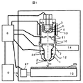
図1に本発明の実施例の一つの概略を示す。
電子源5は材料Zr/O/Wからなるショットキー電子源で1600から1800Kに加熱し、サプレッサ電極6と引き出し電極4により、電子線である電子線プローブ20を形成する電子銃部分を構成している。電子線プローブ20は、試料基板25に入射する際に、電子源側に配置された対物レンズ内側電極3と試料側に配置された対物レンズ試料側電極2からなる静電型の対物レンズにより収束し、直径が30nmから2nm程度の微細な電子線プローブとなる。これを偏向器24によりx、y方向にスキャンし、出てきた二次電子あるいは反射電子を電子検出器7で検出し、電気信号に変換してコントローラ8で信号処理し、ディスプレー9にSEM像を表示する。
FIG. 1 shows an outline of an embodiment of the present invention.
The
SEMカラムは長さ20cm直径7cm程度とコンパクトなハウジング12中に収められ、移動手段14により試料表面上を移動し観察場所を変える。この場合試料ステージ15は試料基板25の固着と、試料バイアス電圧Vsの印加が主な用途であり、高さ、傾き、位置等を移動させる試料移動機構27を備える場合もある。全体は真空容器16中に収められ、真空排気されている。装置を組み立てあるいはメンテナンスを行い真空に立ち上げる場合は、電子源5周りを10-7Pa程度の超高真空雰囲気にする必要があるため、次のような手順をとる。真空容器16の排気開始後、ヒータ13に通電し100℃程度に加熱、これによりバルブ10が開き、カラム内部のガス排気が促進される。バルブ10の動作説明は図2に示す。室温では図2(a)のように、隔壁12に開いた排気穴を弁19が塞いでおり、バイメタル18のばねにより押し付けられているのでガスの出入りは防がれている。100℃以上に加熱すると図2(b)のように、バイメタルが曲がり、弁19は隔壁12から離れるので、高いコンダクタンスで高圧力側から低圧力側にガスが流れる。このバルブ10を開きながら真空容器全体で10-4から10-5Pa程度に排気し、1から2時間程度した後、ヒータ13の通電電力を上げ、カラム下部で200℃、電子源近くで400℃で1時間以上加熱する。この加熱により、カラム内部の吸着ガスが減ると共に、カラム内部に配した非蒸発ゲッタポンプ11が活性化し内蔵ポンプとして稼働する。
The SEM column is housed in a
その後室温に冷却しバルブ10を閉じる。これにより、電源周りとハウジング12の外側とでは、電子線の通る穴を介して2段の差動排気状態となるので、電子源は超高真空雰囲気に保たれる。非蒸発ゲッタポンプは所定量ガスを吸着するとポンプ作用が低下するので必要な場合には再度加熱すればポンプとして活性化する。吸着ガスが半年から1年程度あってもポンプ作用を保つように、ガスの流入穴径とゲッタポンプ量を調整しておけば、電子源5の交換のときに同時に非蒸発ゲッタポンプの再活性化を行なうことで、メンテナンス工数を減らし、装置稼働時間を長く取ることができる。非蒸発ゲッタポンプ11は、メンテナンス時に交換する方式としてもよい。
Thereafter, it is cooled to room temperature and the
本構成では、大きな試料、例えば直径300mm以上のSi基板、あるいは一辺が1m以上の平面ディスプレー用の基板であっても、真空容器16は試料ステージ15の大きさに、周辺の空間と真空容器の厚み程度のサイズで済むという利点がある。従来の半導体用のSEMでは、試料の全領域を観察するには、試料ステージの移動距離を縦横共に試料の幅の2倍の距離とする必要がある。カラム移動式である本発明の場合は、従来の装置の約1/4の大きさですむという利点がある。なお、試料を大気から真空に入れるための準備室を設けた場合は1/2以下のサイズとなる。
In this configuration, even if it is a large sample, for example, a Si substrate having a diameter of 300 mm or more, or a flat display substrate having a side of 1 m or more, the
図3(a)は電子光学系のより詳しい説明図である。
ドリフト管1への印加電圧Vpは4kVから20kVであり、これはワーキングディスタンスWDにより変わる。WD=5mmの場合は5kV程度、WD=2mmの場合は10kV程度、WD<2mmの場合は10から20kVとして用いる。電子源5には、電子線を加速させるための加速電圧Vaが印加され、本実施例ではVaは−1kV程度である。なお、Vaの範囲は−500V程度から−3kV程度が好適である。ドリフト管内には、入射された電子が一定速度で動くドリフト領域が形成されており、ドリフト領域内では、電子は、ドリフト管への印加電圧Vpと電子源1に印加する加速電圧Vaの絶対値の和のエネルギーに保たれる。試料にはサンプルバイアスVsが印加される。Vsを調整することにより、二次電子の検出感度を調整することができ、本実施例では、Vsは0から−2kV程度であった。ドリフト管の下面には対物レンズ内側電極3が配置される。対物レンズ内側電極3は、ドリフト管下面部と一体化されている場合もある。対物レンズ内側電極3には、ドリフト管への印加電圧Vpと同一の電圧が印加される。対物レンズ内側電極3と対物レンズ試料側電極2の間の電界を調整することで、対物レンズのレンズ主面の位置を対物レンズ試料側電極2と試料との間に形成する。対物レンズよりも試料側にレンズ主面を形成することでWDを小さくしてもレンズ収差を小さくすることができる。
FIG. 3A is a more detailed explanatory view of the electron optical system.
The applied voltage Vp to the
また、絶縁体を含む試料の場合、電子線照射による試料のチャージアップ電位が高くなり測定のさまたげとならないように、対物レンズ試料側電極2と試料基板25間の電界が250V/mmを超えないような電界が望ましい。試料基板25で発生した二次電子は、対物レンズに向かい、一部が穴を抜けてドリフト管1中に導かれる。このとき加速によるレンズ作用があるので、図3中の、実線のAや破線のBのような軌道をたどり電子検出器7に入射する。二次電子の軌道の違いは、ワーキングディスタンスWD, 対物レンズ長Lobjと、印加電圧のVs,Vpで決定される。ここで、電子検出器7は図4に示す半導体検出器を用いている。電子検出器は4分割式で、穴径はDh、検出領域の内径D1、外径D2である。穴径Dhは電子線プローブ20の障害とならないサイズであり、0.1mm以上あれば良く、アライメントも考慮して実用上0.7mm以上が望ましい。検出領域の内径D1は、大きすぎると二次電子線の収率が落ちるのでできうる限り小さい方が良く、穴径Dhとの兼ね合いで1.2mm程度が望ましい。実用上は、1mmから6mmの範囲で選べばよい。その場合、内径D1の値に対して、対物レンズ内側電極3の上面から検出器7までの距離Ldetは十分大きくとり、10から60倍とすることが望ましい。
In the case of a sample including an insulator, the electric field between the objective lens sample-
一方、外径D2は、できうる限り大きい方が二次電子を捕獲する領域が広くなるが、小型のカラムサイズとの兼ね合いがあるので、最適条件を選ぶ必要がある。対物レンズ内側電極3の上面から検出器7までの距離Ldetは、図3のA軌道をとる場合、
D2=(1+2 Ldet/Lobj)Dobj (式1)
が有効で、これより外には電子が来ない。また、B軌道をとる場合、
D2=(1+ Ldet/Lobj)Dobj (式2)
となる。実用的にはVsを考慮してこれらの値の±20%以内のサイズを選べばよい。
また、D2が定められている場合には上記(式1)と(式2)を基にLdetを定めても良い。
On the other hand, when the outer diameter D2 is as large as possible, the region for capturing secondary electrons becomes wider. However, since there is a tradeoff with a small column size, it is necessary to select an optimum condition. The distance Ldet from the upper surface of the
D2 = (1 + 2 Ldet / Lobj) Dobj (Formula 1)
Is effective, and no electrons come outside. Also, when taking B orbit,
D2 = (1+ Ldet / Lobj) Dobj (Formula 2)
It becomes. In practice, a size within ± 20% of these values should be selected in consideration of Vs.
When D2 is determined, Ldet may be determined based on the above (Formula 1) and (Formula 2).
0.5Lobj((D2/Dobj)−1)≦ Ldet ≦Lobj((D2/Dobj)−1) (式3)
さらに、電子光学系の条件として、以下の式を満足するという条件に沿って各値を設定する。
0.5Lobj ((D2 / Dobj) -1) ≤Ldet≤Lobj ((D2 / Dobj) -1) (Formula 3)
Furthermore, each value is set as a condition of the electron optical system in accordance with a condition that the following expression is satisfied.
0.01mm < Dobj < Lobj/2,
50 < |Va| < 2000, (式4)
4 ≦ Vp/|Va| ≦ 20
Vp/|Va| が4を下回ると電子ビーム径は20から30 nmを超え、これは、従来の減速型静電レンズで十分達成可能である。
0.01mm <Dobj <Lobj / 2,
50 <| Va | <2000, (Formula 4)
4 ≤ Vp / | Va | ≤ 20
When Vp / | Va | is less than 4, the electron beam diameter exceeds 20 to 30 nm, which is sufficiently achievable with a conventional decelerating electrostatic lens.
本発明は、電子レンズ中で電子が加速する、いわゆる加速型静電レンズを用いることで高感度でかつ高分解能化を達成するものであり、これを発揮するためにはVp/|Va| が4以上の領域とすることが望ましい。Vp/|Va|を大きくしていくと対物レンズはより短焦点になり、電子光学系の収差が小さくなっていくことが知られており、この結果、電子ビーム径の小さい、すなわち分解能の高いものが得られる。この上限値は、対物レンズ試料側電極2と対物レンズ内側電極3間の耐圧で決まり、例えば、Lobj=5mm程度の場合、材料の肉厚を1.5mm程度とすると、空隙は2 mmとなり、放電しないで使える電界の目安である10 kV/mmより、最大電圧は20 kVとなる。この実用的なVaの値は1 kVでWDが約1mm、収差は2nm~4 nmであるので、Vp/|Va| の上限として20が得られる。ここで、Lobjを大きくすれば耐電圧は上がるが電子レンズ条件を一定にするにはそれに比例して大きな電圧印加が必要となる。ここでVpが20 kVを超えると、例えば、大気中の電源ケーブルから真空槽内に電気を導入するフィードスルーのガイシは沿面放電を防ぐために大きなものが必要となり、さらに大気中でのコロナ放電防止のためのガス封止や樹脂封入などが必須となるので、小型のSEM構造を得ようとする本実施例からは望ましくない条件となる。したがって、Vp/|Va| の上限としておよそ20が望ましい。
The present invention achieves high sensitivity and high resolution by using a so-called accelerating electrostatic lens in which electrons are accelerated in an electron lens. To achieve this, Vp / | Va | It is desirable to have 4 or more areas. As Vp / | Va | is increased, the objective lens becomes shorter in focus and the aberration of the electron optical system is known to decrease. As a result, the electron beam diameter is small, that is, the resolution is high. Things are obtained. This upper limit value is determined by the pressure resistance between the objective lens
本実施例では、例えば、Lobj=5.5mm, Dobj=0.8mm, Ldet = 60mm, WD = 2mmの条件では、Vp = 10kV, Vfは1kV〜3kVがよく、このときの二次電子の条件を図7に示す。試料基板25から放出する二次電子は様々なエネルギーと放出角ψを持ち、それぞれ異なる軌道を取るが、電子検出器7に至るには対物レンズの穴を抜ける必要がある。放出角が大きいと対物レンズにさえぎられて上方に出てこられなくなる。ここで放出角ψとは、図8に示すように、試料表面の法線と、試料から放出される電子の方向との角度である。この対物レンズ上に抜けられる電子の放出角の最大値ψmaxは、二次電子エネルギーとVsにより変わり、図7(a)に示す関係となる。また、D1=1.2mmの場合、放出角の最小値ψminより小さいものはD1より内側に到達するので検出されない。このψminと二次電子エネルギーとVsの関係は、図7(b)となる。二次電子放出量は、Cosψに比例するので、これを全方位でψmaxからψminまで足し合わせると、二次電子の各エネルギーの収率はVsにより図7(c)に示すとおりとなる。これに二次電子のエネルギー分布をかけて二次電子収率とし、Vs依存性を示したものが図7(d)Aの曲線である。この図から、二次電子収率の最適条件はVs = −300 V付近であり、この条件で用いれば最高の感度が得られる事がわかる。
In this embodiment, for example, under the conditions of Lobj = 5.5 mm, Dobj = 0.8 mm, Ldet = 60 mm, and WD = 2 mm, Vp = 10 kV and Vf are preferably 1 kV to 3 kV. Shown in 7. The secondary electrons emitted from the
ここで、図7(c)をみると、検出器に到達する電子の収率はあるエネルギーでピークとなり、このピーク位置のエネルギーはVsによって変わり、−Vsが大きいほど高エネルギー側にシフトしていくことがわかる。この効果は、本二次電子検出系がエネルギーフィルタとして機能することを示している。これを利用して、表面の帯電電位の定量評価あるいは、材料の二次電子のエネルギー分布の違いによる判別などが行なえる。例えば、試料表面の一部が局所的に負に帯電した場合、放出される二次電子エネルギーは帯電分だけ高くなるので-Vsが小さいときは信号量が下がり、大きくなると信号量が増える、図7(d)中の破線Bのようになる。一方、正に帯電した場合、エネルギー分布は低エネルギー側にシフトするので-Vsが小さいところで信号量のピークとなる点線Cのようになる。この帯電量と二次電子信号量-Vs曲線との関係は、装置条件に固有のものであるから、測定条件ごとに両者の関係を計算もしくは実測で求めておくことにより、帯電電位の定量的評価ができるという利点がある。
なお、この場合、二次電子が検出器7に到達するときの最外径はVsによって表1に示すようになっているので、D2は10mm程度のものがあれば良く、これは、図3の軌道Bに相当する。
Here, looking at FIG. 7 (c), the yield of electrons reaching the detector peaks at a certain energy, and the energy at this peak position varies depending on Vs, and shifts to the higher energy side as -Vs increases. I can see it going. This effect indicates that the secondary electron detection system functions as an energy filter. By utilizing this, it is possible to perform quantitative evaluation of the charged potential of the surface or discrimination based on the difference in energy distribution of secondary electrons of the material. For example, when a part of the sample surface is locally negatively charged, the secondary electron energy released increases by the amount of charge, so the signal amount decreases when -Vs is small, and the signal amount increases when it increases. It becomes like a broken line B in 7 (d). On the other hand, when positively charged, the energy distribution shifts to the low energy side, so that the dotted line C is the peak of the signal amount when -Vs is small. Since the relationship between the charge amount and the secondary electron signal amount-Vs curve is specific to the instrument conditions, the charge potential can be quantitatively determined by calculating or measuring the relationship for each measurement condition. There is an advantage that it can be evaluated.
In this case, since the outermost diameter when the secondary electrons reach the

半導体を用いた電子検出器7は、図4に示した、電子を検出する面S1,S2,S3,S4を試料側に向けて置かれ、各々独立なダイオード型電子検出器として機能する。この検出器7の電位はドリフト管1の電位Vpと同電位に保たれる。ここで同電位とは全く同一の電位のみならず±10V程度の誤差は許容される。検出器の検出面S1,S2,S3,S4各々には、バイアス電圧Vbを重畳させる。Vbは、0から−100Vの間から選ばれる。検出面S1,S2,S3,S4にVbを印加して流れる電流を測定するために電流検出器26を設け、この出力:Out端子からコントローラ8に二次電子信号として伝達される。電流検出器として、例えば図5(a)の構造を用いればよい。電子検出器7のS1,S2,S3,S4からフィードスルーを介して大気中に取り出した線はSensor端子に入力され、一方Vpに重畳したVb電圧はBias端子に入力される。
The
オペアンプ50とセンス抵抗Rsで構成された電流電圧変換回路により、SensorをBiasと同電位に保ちつつ流れる電流に−Rsを乗じた電圧が出力される。これをADコンバータを通してデジタル信号に変換する。ここまでは高電圧Vpが重畳しているので、コントローラ8の信号処理系と電位を合わせるために、光アイソレータを設ける。ここで、Rsの値は、測定信号強度により最適なものを選ぶ必要があり、条件が変わる場合は、このRsを可変式とすると便利である。また、図5(a)では光アイソレータとしてホトカプラを用いているが、光ファイバで配線してもよい。また、光を用いずとも、トランスによるアイソレーションでも同様に用いられる。さらに、高い精度が不要な場合は、デジタル信号に変換せずとも、アナログ信号のまま光やトランスのアイソレータを用いても良く、その場合安価にできるという利点がある。また、アナログ信号の場合は、振幅変調、周波数変調等により高周波に変換すると精度が高くなるという利点がある。
A current-voltage conversion circuit composed of the
また、信号強度が十分にある場合には、図5(b)に示すように、センス抵抗RsとデカップリングコンデンサCdを用いたシンプルな回路でもよく、この場合、安価でコンパクトとなる。また構造が単純なため、真空装置内に設置できるので、高電圧配線の数が少なくてすむという利点がある。より高周波に対応するためには、オペアンプ50を追加し図5(c)のような回路としてもよい。この場合高周波成分の信号がBias側に流れないようにコイルLLを介して電位を与えている。
If the signal strength is sufficient, as shown in FIG. 5B, a simple circuit using a sense resistor Rs and a decoupling capacitor Cd may be used. In this case, it is inexpensive and compact. Further, since the structure is simple, it can be installed in a vacuum apparatus, so that there is an advantage that the number of high voltage wirings can be reduced. In order to cope with higher frequencies, an
試料基板25から発生する反射電子は、ワーキングディスタンスWDが2mm以上の場合には9割程度が対物レンズ試料側電極2に衝突するので、図8のように、対物レンズ試料側電極2の下面に反射電子検出器80を置くとよい。この場合、1kV程度の低加速でも感度のある検出器で、かつ厚さが2mm以下のものが望ましく、半導体検出器の低加速用のものか、MCP(マルチチャンネルプレート)のようなものが用いられる。また、ワーキングディスタンスWDを2mm以下にすると、多くの反射電子が対物レンズの穴を抜けてドリフト管1中に入るので、WDにより二次電子と反射電子情報を選んで取得することができる。
About 90% of the reflected electrons generated from the
本実施例においては、電子検出器7としてドーナツ形で、4分割のものを用いたが、これに限らず、直径方向に細分されているものを用いれば、より詳細なエネルギー分布を知ることができる。あるいは、2分割や分割していないものを用いても良い。さらに、高速動作のためにより小さく作り、穴および分割のない検出器を電子線プローブ20が通る軸をはずして置いてもよい。この場合、検出器の静電容量を小さくできるので高速での画像取得が可能である。たとえば、図9に示すように、ドリフト管1中にWienフィルタ90を入れ、電子線プローブ20は直進する磁界Bw、電界Ewを条件とし、試料基板25から来る二次電子の中心軌道92や反射電子の中心軌道91を曲げて電子検出器にもたらすと、高感度な測定が実現される。このときの条件は、電子線プローブの速度をvとしたとき、v×Bw=Ewであり、この条件のままBw、Ewの強度を調節すると、運動エネルギーの違いにより二次電子と反射電子をそれぞれ別々に選択して観測することができるというメリットがある。
In this embodiment, the
なお、この効果は、Wienフィルタを使わなくとも、ドリフト管内部に軸対称構造の減速電極のような電界コントロール電極を置いても可能で、この場合、電子線プローブ20の軌道には大きな影響を与えない程度の電界を形成し、これにより二次電子および反射電子の軌道の広がりを調節して検出器7で最良の条件を得る。この場合、電極1枚の追加で行なえるのでより簡便な構造とすることができる。なお、この場合検出すべき電子は同軸上に広がるので、検出器7は、図4のようなドーナツ形のほうが望ましい。
また、本実施例においてはドリフト管内に電子検出器を備えた構造としたが、図3(b)のようにドリフト管内上壁と電子検出器を一体とさせても良い。ドリフト管と電子検出器を一体とすることで製造工程を短縮化できるという効果がある。
This effect can be achieved without using a Wien filter, and an electric field control electrode such as an axially symmetric deceleration electrode can be placed inside the drift tube. In this case, the trajectory of the
In the present embodiment, the electron detector is provided in the drift tube. However, the inner wall of the drift tube and the electron detector may be integrated as shown in FIG. The manufacturing process can be shortened by integrating the drift tube and the electron detector.
本実施例においては、電子ビームのスキャン、軸あわせ、およびスティグマ調整をドリフト管1の周りに配したコイル24からの磁場で行なう。このため、ドリフト管1の材料は非磁性体であることが望ましく、Tiや非磁性ステンレスなどが用いられる。あるいは、SiO2やAl2O3等の絶縁体材料を主成分とする碍子構造の中に同軸形状の穴を設け、この内壁に導電性の被覆を施したものを用いても同様の効果がある。 また、偏向には磁界を用いずに電界を用いても良く、例えば静電8極の偏向器を2段高加速領域に配しても同様の効果がある。この場合、磁界式よりも高速での動作に向いている。
In the present embodiment, scanning of the electron beam, axial alignment, and stigma adjustment are performed by a magnetic field from a
本実施例では、電子源としてショットキー型電子源を用いたが、他の電子源を用いても良く、例えば、W<310>やカーボンナノチューブのような電界放射電子源60を図6のように引き出し電極4と対向させてフィラメント61上にマウントしてもよい。この場合、電子銃構造にサプレッサ電極は不要となるのでより簡便な構造となる。また、電子源のソースサイズが10nmから3nm程度ときわめて小さく、さらにエネルギー分布も最低で0.2eVとなるので、色収差が小さく、極めて高分解能化が達成されるという利点がある。
In this embodiment, a Schottky electron source is used as the electron source, but other electron sources may be used. For example, a field
また、本実施例においては電子線プローブの収束に静電レンズを用いているが、静電レンズが主な収束手段であれば、小型のコイルや永久磁石などで磁界を重畳しても良く、例えば、試料と対物レンズ近傍に軸対称の磁場を形成すると、二次電子が磁力線に沿ってカラム中に戻るので、二次電子の感度が高いものが得られる。 あるいは、電子源近傍に同軸の磁界を重畳することで、大きなプローブ電流が得られるという利点がある。あるいは、ソースサイズの小さい電界放射型電子源の場合には磁化の重畳により収差が小さくなるのでより高分解能となるという利点がある。 In this embodiment, an electrostatic lens is used to converge the electron beam probe. However, if the electrostatic lens is the main focusing means, a magnetic field may be superimposed using a small coil or permanent magnet, For example, when an axially symmetric magnetic field is formed in the vicinity of the sample and the objective lens, secondary electrons return to the column along the lines of magnetic force, so that a high sensitivity of secondary electrons can be obtained. Alternatively, there is an advantage that a large probe current can be obtained by superimposing a coaxial magnetic field in the vicinity of the electron source. Alternatively, in the case of a field emission electron source having a small source size, there is an advantage that higher resolution is achieved because aberrations are reduced by superposition of magnetization.
本発明の実施例の一つの模式図を図10に示す。
基板上にナノパターンを形成する手段の一つ、ナノインプリント用の金型100の検査装置に応用した例である。ナノインプリント法とは、対象とするSi、プラスチック、ガラス等の基板上に熱硬化性あるいは光硬化性などの硬化性を持った樹脂の薄膜を形成し、これに金型を押し付けて樹脂を整形したまま、熱あるいは紫外線などにより樹脂を硬化させ、その後金型を剥離してナノパターンを形成する工程である。紫外線を用いること、および熱膨張や塑性変形を嫌うために金型はガラスや石英で作られている。この工程では、剥離しやすさ、パターン精度等のために金型の三次元的な構造が重要である。この金型の検査には、光による方法、例えば共焦点顕微鏡では寸法が小さすぎるので測定は困難である。また、従来のSEMによる三次元検査装置では、加速電圧が高くチャージアップが防ぎきれないこと、および試料室が大きくなり、装置自体が大きく、コスト高になるといった問題がある。
One schematic view of an embodiment of the present invention is shown in FIG.
This is an example applied to an inspection apparatus for a
図10の構成は、図1と同じ本発明によるSEMカラム101が移動手段14上に装着され、ナノ金型100表面を下からSEM観察する。SEM観察とカラム移動は同時に行なうこともできる。ここで、4分割の電子検出器7の4つのセンサS1,S2,S3,S4から別々に4個の電流検出器26から二次電子信号を取り出す。この信号に基づいて表面の三次元構造をコントローラ8中で構築しディスプレー8に表示する。図11を用いて三次元構造の構築方法を説明する。
In the configuration of FIG. 10, the
図11(a)のように、試料基板25表面に凹凸がある場合、例えば、電子線プローブが当たっている面が試料基板の法線から角度θ傾いているときには、試料から放出される二次電子分布の中心もθ傾く。本発明によるSEMカラムは静電レンズを用いているので二次電子軌道の回転が無く、電子放出方位の偏りがそのまま検出器7に反映される。さらに、図11(a)に示されるように、試料基板法線から見た電子の放出角ψと、検出器7に衝突する位置(この場合軸中心からの距離)はほぼ1対1に対応する。したがって、放出電子の分布中心が傾くと、検出器7のセンサS1、S2で検出される強度が異なってくる。 この関係は図11(b)に示されるように、センサS1,S2で検出される電子は放出角ψminからψmaxの範囲であるが、分布の中心がθずれているので、強度に差が出る。二次電子の角度分布は放出する表面に対してコサイン分布となるので、
S1、S2上での電子の検出強度はそれぞれa(ψ)、b(ψ)とすると、図中の曲線は式5となる。
As shown in FIG. 11A, when the surface of the
If the detected intensities of electrons on S1 and S2 are a (ψ) and b (ψ), respectively, the curve in the figure is expressed by
ここで、f(ψ)はカラムの検出効率のψ依存性、g(θ)は試料表面での二次電子イールドである。f(ψ)は、ψminからψmaxの範囲ではほぼ一定として扱える。また、1kV付近の低加速では電子のもぐりこみが浅いので、g(θ)はおおむね一定として扱える。通常は、傾きθの面はx方向とy方向の様々な方位をとりうるので、これをθx、θyと分解して、放出角空間ψx、ψy上で、センサS1,S2,S3,S4への写像として図11(c)のように書くことができる。このときのS1、S2上での検出強度はそれぞれ、次式となる Here, f (ψ) is the ψ dependency of the detection efficiency of the column, and g (θ) is the secondary electron yield on the sample surface. f (ψ) can be treated as almost constant in the range from ψmin to ψmax. In addition, at a low acceleration around 1 kV, the electron trapping is shallow, so that g (θ) can be treated as being almost constant. Usually, since the surface of the inclination θ can take various orientations in the x direction and the y direction, it is decomposed into θx and θy, and is sent to the sensors S1, S2, S3, and S4 on the emission angle spaces ψx and ψy. As a map of, it can be written as shown in FIG. The detected intensity on S1 and S2 at this time is as follows:
S3,S4からのデータの場合はこの式6のxとyを入れ替えればよい。
この式6から、簡便にθとθxが次のように求められる。
In the case of data from S3 and S4, x and y in this
From this
この式7、8より、測定値から表面の傾きを定量化することができる。
ここで、a(ψ,0), b(ψ,0)は平らなθ=0の表面における実測値である。なお、S3,S4からのデータにより、このxとyを入れ替え、θとθyが得られる。
より精度を高める場合は、測定系毎に図11(c)の各センサS1,S2,S3,S4で検出する電子量とθの関係を計算あるいは実測してデータベース化しておき、これと比較して決めるとよい。
以上の方法により4個のセンサの信号から求めたθ、θx、θyと、電子線プローブを走査した距離情報により3次元構造が計算により求められる。
From these
Here, a (ψ, 0) and b (ψ, 0) are actually measured values on a flat θ = 0 surface. Note that x and y are exchanged based on the data from S3 and S4 to obtain θ and θy.
In order to further improve the accuracy, the relationship between the amount of electrons detected by each sensor S1, S2, S3, S4 in FIG. It is good to decide.
A three-dimensional structure is obtained by calculation from θ, θx, θy obtained from the signals of the four sensors by the above method and distance information obtained by scanning the electron beam probe.
なお、本実施例のようにセンサが4分割の場合、得られる情報は重複しているので、これらの平均を取るあるいは補完することで、よりノイズの少ない、精度の高い三次元像が得られる。4分割以外でも、例えば2分割や8分割などでも同様に三次元構造が求められる。なお、2分割の場合は、1点からの測定値ではすべての傾き情報が得にくい場合があるが、電子線プローブをスキャンしているので、近隣のデータと比較することで三次元構造を計算することができる。例えば、検出器の分割が、x軸の+側と−側の場合、一点での測定値からy方向の傾きθyも求められるが精度は低くなる。しかし試料表面が連続的に変化している場合は、近くの場所ではθyが連続的に変化する場所と、θxが連続的に変化する場所が必ずあるので、精度の低いデータを補完することができる。 In addition, when the sensor is divided into four as in the present embodiment, the obtained information is overlapped. Therefore, by taking an average of these or complementing them, a three-dimensional image with less noise and high accuracy can be obtained. . A three-dimensional structure is also obtained in the same manner in other than four divisions, such as two divisions or eight divisions. In the case of two divisions, it may be difficult to obtain all the tilt information from the measurement value from one point, but since the electron probe is scanned, the three-dimensional structure is calculated by comparing with the neighboring data. can do. For example, when the detector is divided on the + side and the − side of the x axis, the inclination θy in the y direction can be obtained from the measured value at one point, but the accuracy is low. However, if the surface of the sample is changing continuously, there are always places where θy changes continuously and places where θx changes continuously in nearby places, so that data with low accuracy can be supplemented. it can.
図10の構造に適応する場合、分解能2nmのカラムを用いると、幅、高さ、溝の側壁の角度など寸法の1/10以下の高精度測定が実現される。また、高速で検査したい場合には、解像度10nmから20nm程度あれば異物や、亀裂などの不良判定は容易に行なえる。その場合、電子のプローブ電流が1nAから100nA以上で、ワーキングディスタンスWDは5mm以上あるので、高速検査に向いている。さらに、高速に検査する場合は、三次元構造まで計算せずとも、各センサからの信号の値およびその変化量から短時間で異常を判定すればよい。例えば、側壁の傾きが十分でない場合は、対象とするセンサからの信号強度の差が小さい。また、穴の深さが十分でないあるいは内部を異物が塞いでいる場合は、信号強度変化が弱いものを判定すればよい。パターン面に傾きがある場合は、各センサ信号の差を見れば判別できる。欠陥パターンが異物によるか溝か判定する場合は、対象とするセンサ信号の強度差や、変化量が逆となる事で容易に判定できる。 In the case of adapting to the structure of FIG. 10, when a column with a resolution of 2 nm is used, high-accuracy measurement of 1/10 or less of dimensions such as width, height, and groove sidewall angle is realized. In addition, when it is desired to inspect at a high speed, a defect such as a foreign object or a crack can be easily determined if the resolution is about 10 nm to 20 nm. In this case, since the electron probe current is 1 nA to 100 nA or more and the working distance WD is 5 mm or more, it is suitable for high-speed inspection. Furthermore, when inspecting at high speed, it is only necessary to determine an abnormality in a short time from the value of the signal from each sensor and the amount of change without calculating the three-dimensional structure. For example, when the inclination of the side wall is not sufficient, the difference in signal intensity from the target sensor is small. If the depth of the hole is not sufficient or if the inside is covered with a foreign substance, it is sufficient to determine that the signal intensity change is weak. If the pattern surface is inclined, it can be determined by looking at the difference between the sensor signals. When determining whether the defect pattern is due to a foreign matter or a groove, it can be easily determined by the difference in the intensity of the target sensor signal and the amount of change being reversed.
また、本発明のSEMは電子線の加速を1kV程度以下で、かつ対物レンズの試料側電極と試料基板25の間には大きな電界はかかっていないので激しいチャージアップは抑制され、表面帯電が±数V以内に制御されるので、金型100表面の損傷や帯電を抑えて精度良く測定できるというメリットがある。
Further, the SEM of the present invention has an electron beam acceleration of about 1 kV or less, and a large electric field is not applied between the sample side electrode of the objective lens and the
本発明を用いれば、三次元計測可能なSEMを提供できるので、本実施例以外にも適用可能である。例えば、半導体や平面ディスプレー用の検査装置や、エッチングや製膜などのプロセス装置内での異物、不良モニタとして用いられる。とくに本発明の装置は小型であるので、試料準備室内に移動手段と共にSEMカラムを設置しておけば良く、新たな試料搬送装置や真空装置などの追加なしにモニタ機能が付加できるという利点がある。 If the present invention is used, an SEM capable of three-dimensional measurement can be provided. Therefore, the present invention can be applied to other than this embodiment. For example, it is used as an inspection device for semiconductors and flat displays, and as a foreign matter and defect monitor in process devices such as etching and film formation. In particular, since the apparatus of the present invention is small in size, it is only necessary to install an SEM column together with the moving means in the sample preparation chamber, and there is an advantage that a monitoring function can be added without adding a new sample transport apparatus or vacuum apparatus. .
より深い穴や、オーバーハングのある段差を観察するためには、図12のようにSEMカラム101を2個備えるとよい。この場合、2個のSEMカラムA,Bは、試料ステージ15の法線に対して対称の位置で、角度ωの傾きを持ち、焦点位置が同じとなるように設置されている。カラムA、Bの間には二次電子検出器120が置かれ、試料からの二次電子を計測する。カラムAとB交互に切り替えることで、二次電子によるステレオ観察が可能となる。さらに、カラムBから放出された電子線プローブにより発生する反射電子の分布122は、試料からの鏡面反射条件にピークを持っているので、カラムA中の電子検出器で観測される。逆に、カラムBの検出器ではカラムAからのプローブによる反射電子が検出されるので、反射電子によるステレオ観察が可能となる。反射電子を用いた場合はカラムA、Bを切り替える必要が無く、連続運転できるという特徴がある。
In order to observe a deeper hole or a step with an overhang, it is preferable to provide two
オーバーハングの観察には図12(b)のように、カラムBからの電子線プローブによる二次電子をカラムBの検出器で測定する。もしくはこのとき発生した二次電子、反射電子の散乱したものを二次電子検出器120で測定してもよい。この構造では、側壁の傾きが垂直から角度ωまで観察可能である。より広い条件に対応するために、SEMカラム101を移動させ、角度ωを可変とするとよい。また、ワーキングディスタンスWDを可変としてもよい。本発明によるカラムが小型でかつ真空装置内に入っているので、これらの可変機構をつけても装置は実用的な大きさで容易に形成できるという利点がある。
For observation of the overhang, secondary electrons from the column B by the electron beam probe are measured by a detector of the column B as shown in FIG. Alternatively, the scattered secondary electrons and reflected electrons generated at this time may be measured by the
図13には本発明をプロセス装置のうち、収束イオンビーム装置に適用した例を示す。
イオン源130で発生したイオンビームプローブ132は加速10kから30kVでイオンビームカラム131中の静電レンズで収束され試料基板25に照射され、所望の領域をイオンビームエッチングにより切り取っていく。これに対し、角度ωの位置に配置された本発明によるSEMカラム101は、移動手段14により、ワーキングディスタンスWDが可変となっている。ワーキングディスタンスWDが5mmから10mmとした場合には、分解能が低くともより広い領域が観察され、かつ試料元素の再付着による汚れを低減できるので、イオンビームを照射中のモニタ、および終点検出として用いられる。さらに試料の、大まかな領域の俯瞰のために使われる。一方、ワーキングディスタンスWDを1mmから5mmと短くするとより高分解能観察が可能となるので、イオンビームで形成した試料の詳細な断面観察が行なえるという利点がある。このとき、二次電子検出はSEMカラム101内部と、別に置いた二次電子検出器120により行なう。
FIG. 13 shows an example in which the present invention is applied to a focused ion beam apparatus in a process apparatus.
The
また、イオンビーム装置のような電子以外の荷電粒子線装置に本発明を応用してもよい。図14は収束イオンビームカラム131のうち静電レンズの一部を電子線のドリフト管1に置き換えたものである。イオン源130の加速電圧10kV〜30kVに対して、ドリフト管1は1kVから10kVが印加されるので、イオンプローブにとっては減速領域となり、ここでレンズ作用を受けたイオンビーム132は試料基板25表面上で収束する。一方、このとき発生する二次電子133にとっては逆にドリフト管1中で加速されるので、図1と同様に、電子検出器7で検出される。
The present invention may also be applied to charged particle beam devices other than electrons, such as ion beam devices. FIG. 14 shows a focused
この結果、本発明を適用することによりコンパクトなイオンビームカラムを提供できる。また、近くにSEMカラムを置き、電子線プローブを照射した場合も同様にイオンビームカラム131中で二次電子検出が可能となるという利点がある。実用上は、電子線プローブによる二次電子の方が量が多いので、SEM像の信号取得用にイオンカラム131が用いられるので、装置全体でコンパクトになるため、プロセス装置や透過電子顕微鏡などの観察装置の準備室に備え付けることが可能である。
As a result, a compact ion beam column can be provided by applying the present invention. Further, there is an advantage that secondary electrons can be detected in the
本発明によるSEMカラムはコンパクトなハウジング中に小型ポンプと二次電子検出器を内蔵できるので、多数並列に並べて使うことができる。
図15には、直径300mmのウエハに対応した検査装置の概略を示す。第1の真空室150と、第2の真空室151があり両者の間を開閉する扉を通り試料基板25はローダーにより出入りすることができる。第2の部屋151は準備室として、大気中から試料基板25を挿入し真空に引いて待機する。第1の真空室150には、本発明によるSEMカラム101が8本結合しておかれ、各カラムの直径は38mmである。このカラムは図1と同じもので、WD5mmの条件で電子線プローブを30nAから100nAと大電流化したもので、分解能は20nmから40nmである。この8本の組をx方向とy方向の移動手段14を用い、例えば図15中の矢印のように移動させて、試料表面のパターン形状、帯電異常などの不良箇所の検査を行なうことができる。この場合、従来のカラム1本のSEM式の検査装置に比べて同じプローブ電流で用いた場合、最大で8倍の高速化が可能となるので、試料の全面を検査しても短時間ですむという利点がある。
それぞれのカラムを接続する際、それぞれの電子光学系で発生した電界あるいは磁界を同一光学系内で遮蔽する遮蔽シールド152をカラム内に配置してもよい。
Since the SEM column according to the present invention can include a small pump and a secondary electron detector in a compact housing, a large number of them can be used in parallel.
FIG. 15 shows an outline of an inspection apparatus corresponding to a wafer having a diameter of 300 mm. There is a
When connecting each column, a
本実施例においてはカラム101を移動させているが、多数並べて広い範囲をカバーしているので、カラムは固定して試料基板25を移動して検査してもよい。この場合カラム1本の場合と比べて試料移動範囲が小さくてすむので、小型高速な検査装置が得られる。
また、本実施例において、第1の真空室150を準備室、第2の真空室151をプロセス室として用いても良い。プロセスとは、たとえば、エッチング、成膜、イオン注入などの工程で主に真空を使うもので、これらは、プロセス後の検査や確認に、一度大気中に取り出す必要があり、電子線で検査する場合には再度真空引きするという工程が必要となる。そのため、準備室もしくは試料を真空導入後の搬送室内にSEMカラムを多数配置して検査すると工程が短縮できるという利点がある。
In this embodiment, the
In this embodiment, the
例えば、図16の装置は、一辺1mから2mの大型の平面ディスプレーパネルの製造装置に応用した例で、搬送室の周りにプロセス室160が4個、予備排気室162が2個接続され、各室間のパネル161の移動は搬送装置163により行なわれる。装置全体は真空ポンプで排気され、各部屋を仕切っているゲートバルブが、試料パネル161出し入れの際に開く。
For example, the apparatus of FIG. 16 is an example applied to a manufacturing apparatus of a large flat display panel having a side of 1 to 2 m, and four
各プロセス室160で処理後に搬送室164中でSEMカラム101により欠陥や異物、プロセス条件の確認などを行なうことが可能になるので、検査工程を大幅に短縮できる、あるいは歩留まりが上がるという効果がある。また、カラムの移動手段14によりカラムを動かして用いることができるので、搬送室内に内蔵して使え、SEM機能を付加しても安価で床面積の増加も抑えられるという利点がある。
After processing in each
以上、実施例をあげて説明したように、本発明を用いれば、ポンプと二次電子検出器を内蔵した超小型で高感度かつ高分解能のSEMが実現される。さらに、超小型で三次元構造の観察を行なうSEM装置や、カラム移動式、マルチカラム式のSEM装置など、高機能の電子線応用装置が実現される。 As described above with reference to the embodiments, if the present invention is used, an ultra-compact, high-sensitivity and high-resolution SEM incorporating a pump and a secondary electron detector can be realized. In addition, highly functional electron beam application devices such as ultra-compact SEM devices that observe three-dimensional structures, column movement type, and multi-column type SEM devices are realized.
1ドリフト管、2対物レンズ試料側電極、3対物レンズ内側電極、4引き出し電極、5電子源、6サプレッサ電極電極、7電子検出器、8コントローラ、9ディスプレー、10バルブ、11非蒸発ゲッタポンプ、12ハウジング、13ヒータ、14移動手段、15試料ステージ、16真空容器、17調整電極、18バイメタル、19弁、20電子線プローブ、21アパーチャプレート、22電子銃部、23ガイシ、24偏向器、25試料基板、26電流検出器、27試料移動機構、50オペアンプ、60電界放射型電子源、61フィラメント、80反射電子検出器、90Wienフィルタ、91曲げられた反射電子の中心軌道、92曲げられた二次電子の中心軌道、100ナノ金型、101本発明のSEMカラム、122反射電子分布、123二次電子分布、120二次電子検出器、130イオン源、131収束イオンビームカラム、132イオンビームプローブ、133イオンビームカラム中の二次電子軌道、150第1の真空室、151第2の真空室、152遮蔽シールド、160プロセス室、161試料パネル、162予備排気室、163搬送装置、164搬送室。 1 drift tube, 2 objective lens sample side electrode, 3 objective lens inner electrode, 4 extraction electrode, 5 electron source, 6 suppressor electrode electrode, 7 electron detector, 8 controller, 9 display, 10 valve, 11 non-evaporable getter pump, 12 Housing, 13 heater, 14 moving means, 15 sample stage, 16 vacuum vessel, 17 adjustment electrode, 18 bimetal, 19 valve, 20 electron beam probe, 21 aperture plate, 22 electron gun section, 23 insulator, 24 deflector, 25 sample Substrate, 26 current detector, 27 sample moving mechanism, 50 operational amplifier, 60 field emission electron source, 61 filament, 80 backscattered electron detector, 90 Wien filter, 91 center trajectory of bent backscattered electrons, 92 bent secondary Electron center orbit, 100 nano mold, 101 SEM column of the present invention, 122 backscattered electron distribution, 12 Secondary electron distribution, 120 secondary electron detector, 130 ion source, 131 focused ion beam column, 132 ion beam probe, secondary electron orbit in 133 ion beam column, 150 first vacuum chamber, 151 second vacuum Chamber, 152 shielding shield, 160 process chamber, 161 sample panel, 162 preliminary exhaust chamber, 163 transfer device, 164 transfer chamber.
Claims (20)
当該荷電粒子線源より放射された荷電粒子線を加速させるための手段と、
ドリフト領域を構成するドリフト管と、
前記荷電粒子線が照射される試料を載置する試料ステージと、
前記試料に荷電粒子線を照射して発生する二次電子または反射電子を検出する検出器と、
前記荷電粒子線の通過する開口部を有する対物レンズとを備え、
該対物レンズは前記ドリフト管と試料ステージの間に配置され、
前記荷電粒子線源は前記ドリフト管の外部に配置され、
前記検出器が前記ドリフト管内に配置されていることを特徴とする荷電粒子線装置。 A charged particle beam source;
Means for accelerating the charged particle beam emitted from the charged particle beam source;
A drift tube constituting a drift region;
A sample stage on which a sample irradiated with the charged particle beam is placed;
A detector for detecting secondary electrons or reflected electrons generated by irradiating the sample with a charged particle beam;
An objective lens having an opening through which the charged particle beam passes,
The objective lens is disposed between the drift tube and the sample stage;
The charged particle beam source is disposed outside the drift tube;
The charged particle beam apparatus, wherein the detector is disposed in the drift tube.
当該荷電粒子線源より放射された荷電粒子線を加速させるための手段と、
ドリフト領域を構成するドリフト管と、
前記荷電粒子線が照射される試料を載置する試料ステージと、
前記試料に荷電粒子線を照射して発生する二次電子または反射電子を検出する検出器と、
荷電粒子線の通過する開口部を備えた対向電極を有する静電型対物レンズと、
該対物レンズは前記試料側に配置された第一の電極と荷電粒子線源側に配置された第二の電極を備え、
前記ドリフト管と前記検出器とを同電位に保つための手段を備え、
前記対物レンズの主面は前記第一の電極と前記試料台との間に形成され、
前記荷電粒子線源は前記ドリフト管の外部に配置され、
前記第二の電極は前記ドリフト管の下面に配置されていることを特徴とする荷電粒子線装置。 A charged particle beam source;
Means for accelerating the charged particle beam emitted from the charged particle beam source;
A drift tube constituting a drift region;
A sample stage on which a sample irradiated with the charged particle beam is placed;
A detector for detecting secondary electrons or reflected electrons generated by irradiating the sample with a charged particle beam;
An electrostatic objective lens having a counter electrode with an aperture through which a charged particle beam passes;
The objective lens includes a first electrode disposed on the sample side and a second electrode disposed on the charged particle beam source side,
Means for maintaining the drift tube and the detector at the same potential;
The main surface of the objective lens is formed between the first electrode and the sample stage,
The charged particle beam source is disposed outside the drift tube;
The charged particle beam apparatus, wherein the second electrode is disposed on a lower surface of the drift tube.
前記第一のカラムと第二のカラムに共通した試料を載置するための試料ステージと、
前記第一のカラムと第二のカラムを移動させるカラム移動機構または前記試料を移動させるための試料移動機構と、
前記第一のカラムと第二のカラムは
荷電粒子線源と、荷電粒子線を加速するための手段と、ドリフト領域を構成するドリフト管と、前記荷電粒子線を前記試料に照射するための静電型対物レンズと、前記荷電粒子線を照射することで前記試料より発生した二次電子または反射電子を検出する検出器とを各々有し、
前記ドリフト管内に前記検出器を備え、
前記荷電粒子線源は各々前記ドリフト管の外部に配置され、
前記第一のカラムと第二のカラムは前記試料ステージ表面に垂直な軸に対して対称に配置され、
前記第一のカラムから前記荷電粒子線を試料に対し照射して発生する反射電子を、第二のカラムにおける検出器によって検出することを特徴とする荷電粒子線装置。 In a charged particle beam apparatus comprising at least a first column and a second column,
A sample stage for placing a sample common to the first column and the second column;
A column moving mechanism for moving the first column and the second column or a sample moving mechanism for moving the sample;
The first column and the second column include a charged particle beam source, a means for accelerating the charged particle beam, a drift tube constituting a drift region, and a static beam for irradiating the sample with the charged particle beam. An electric objective lens, and a detector for detecting secondary electrons or reflected electrons generated from the sample by irradiating the charged particle beam,
Comprising the detector in the drift tube;
The charged particle beam sources are each disposed outside the drift tube;
The first column and the second column are arranged symmetrically with respect to an axis perpendicular to the sample stage surface;
A charged particle beam apparatus, wherein reflected electrons generated by irradiating a sample with the charged particle beam from the first column are detected by a detector in the second column.
前記複数のカラムに共通した試料を載置する試料ステージと、
前記複数のカラムを移動するための移動機構または前記試料を移動させるための試料移動機構と、
前記複数のカラムは
荷電粒子線源と、荷電粒子線を加速するための手段と、ドリフト領域を構成するドリフト管と、前記荷電粒子線を前記試料に照射するための静電型対物レンズと、前記荷電粒子線を照射することで前記試料より発生した二次電子または反射電子を検出する検出器とを各々有し、
前記荷電粒子線源は各々前記ドリフト管の外部に配置され、
前記ドリフト管内に前記検出器を備えていることを特徴とする荷電粒子線装置。 In a charged particle beam device in which a plurality of columns are arranged in a vacuum chamber,
A sample stage for mounting a sample common to the plurality of columns;
A moving mechanism for moving the plurality of columns or a sample moving mechanism for moving the sample;
The plurality of columns include a charged particle beam source, means for accelerating the charged particle beam, a drift tube constituting a drift region, an electrostatic objective lens for irradiating the charged particle beam to the sample, Each having a detector for detecting secondary electrons or reflected electrons generated from the sample by irradiating the charged particle beam,
The charged particle beam sources are each disposed outside the drift tube;
A charged particle beam apparatus comprising the detector in the drift tube.
前記対物レンズは前記試料より発生する二次電子または反射電子を加速させる手段を備えることを特徴とする荷電粒子線装置。 The charged particle beam apparatus according to claim 1,
The charged particle beam apparatus, wherein the objective lens includes means for accelerating secondary electrons or reflected electrons generated from the sample.
前記対物レンズは試料側に配置された第一の電極と荷電粒子線源側に配置された第二の電極を備えた静電型対物レンズであって、
前記第二の電極は前記ドリフト管の下面と一体形成されることを特徴とする荷電粒子線装置。 The charged particle beam apparatus according to claim 1,
The objective lens is an electrostatic objective lens including a first electrode disposed on the sample side and a second electrode disposed on the charged particle beam source side,
The charged particle beam device, wherein the second electrode is integrally formed with a lower surface of the drift tube.
前記対物レンズの主面は、前記対物レンズと前記試料ステージとの間に形成されることを特徴とする荷電粒子線装置。 The charged particle beam apparatus according to claim 1,
The charged particle beam apparatus according to claim 1, wherein a main surface of the objective lens is formed between the objective lens and the sample stage.
前記荷電粒子線源と、荷電粒子線を加速させる手段と、ドリフト管と、対物レンズと、検出器とを含むカラムを備え、
該カラムを移動させるカラム移動機構を備えることを特徴とする荷電粒子線装置。 In the charged particle beam device according to claim 1 or 2,
A column including the charged particle beam source, means for accelerating the charged particle beam, a drift tube, an objective lens, and a detector;
A charged particle beam apparatus comprising a column moving mechanism for moving the column.
前記試料を移動させる試料ステージ移動機構を備えることを特徴とする荷電粒子線装置。 In the charged particle beam device according to claim 1 or 2,
A charged particle beam apparatus comprising a sample stage moving mechanism for moving the sample.
前記ドリフト管内における前記第二の電極から前記検出器までの距離Ldetは
前記第一の電極と第二の電極との距離Lobjと、前記対物レンズの開口部の大きさDobjと、前記検出器の検出領域の外径D2から、
The distance Ldet from the second electrode to the detector in the drift tube is the distance Lobj between the first electrode and the second electrode, the size Dobj of the opening of the objective lens, and the detector From the outer diameter D2 of the detection area,
前記ドリフト管への印加電圧と、荷電粒子線源への印加電圧と、試料への印加電圧とを制御するコントローラを有することを特徴とする荷電粒子線装置。 In the charged particle beam device according to any one of claims 1 to 4,
A charged particle beam apparatus comprising a controller for controlling an applied voltage to the drift tube, an applied voltage to a charged particle beam source, and an applied voltage to a sample.
前記ドリフト管への印加電圧は4kV〜20kVの正電圧であることを特徴とする荷電粒子線装置。 In the charged particle beam device according to any one of claims 1 to 4,
The charged particle beam apparatus characterized in that the voltage applied to the drift tube is a positive voltage of 4 kV to 20 kV.
前記領域はドリフト領域であって、
該ドリフト領域は、前記コントローラにより各々の印加電圧を制御することによって形成されることを特徴とする荷電粒子線装置。 In the charged particle beam device according to any one of claims 1 to 4,
The region is a drift region,
The charged particle beam device is characterized in that the drift region is formed by controlling each applied voltage by the controller.
前記検出器は複数の独立した検出領域を有し、該複数の検出領域から各々独立して信号を取り出す手段を有することを特徴とする荷電粒子線装置。 In the charged particle beam device according to any one of claims 1 to 4,
The charged particle beam apparatus according to claim 1, wherein the detector has a plurality of independent detection regions, and has means for independently taking out signals from the plurality of detection regions.
前記試料に荷電粒子線を照射して発生した二次電子と反射電子を独立に検出する手段を備えることを特徴とする荷電粒子線装置。 In the charged particle beam device according to any one of claims 1 to 4,
A charged particle beam apparatus comprising means for independently detecting secondary electrons and reflected electrons generated by irradiating the sample with a charged particle beam.
前記二次電子と反射電子を独立に検出する手段とは、対物レンズ下面に配置された反射電子検出器であることを特徴とする荷電粒子線装置。 In the charged particle beam device according to any one of claims 1 to 4,
The charged particle beam apparatus according to claim 1, wherein the means for independently detecting the secondary electrons and the reflected electrons is a reflected electron detector disposed on the lower surface of the objective lens.
前記二次電子と反射電子を独立に検出する手段とは、前記ドリフト管の内部配置された電界コントロール電極またはWienフィルタであることを特徴とする荷電粒子線装置。 In the charged particle beam device according to any one of claims 1 to 4,
The charged particle beam device according to claim 1, wherein the means for independently detecting the secondary electrons and the reflected electrons is an electric field control electrode or a Wien filter disposed inside the drift tube.
前記荷電粒子線源と引き出し電極を含む電子銃部を備え、
該電子銃部を真空排気するための非蒸発ゲッタポンプと該非蒸発ゲッタポンプ加熱手段を有することを特徴とする荷電粒子線装置。 In the charged particle beam device according to any one of claims 1 to 4,
An electron gun unit including the charged particle beam source and extraction electrode;
A charged particle beam apparatus comprising: a non-evaporable getter pump for evacuating the electron gun unit; and a non-evaporable getter pump heating unit.
前記電子銃部の真空隔壁の一部にガスのバイパス手段を有することを特徴とする荷電粒子線装置。 The charged particle beam device according to claim 18,
A charged particle beam apparatus comprising gas bypass means in part of a vacuum partition wall of the electron gun section.
前記ガスのバイパス手段として、バイパス穴とこれを開閉する加熱変形素子とを設けることを特徴とする荷電粒子線装置。 The charged particle beam device according to claim 19,
A charged particle beam apparatus comprising a bypass hole and a heating deformation element that opens and closes the bypass hole as the gas bypass means.
Priority Applications (2)
| Application Number | Priority Date | Filing Date | Title |
|---|---|---|---|
| JP2004297117A JP2006114225A (en) | 2004-10-12 | 2004-10-12 | Charged particle beam device |
| US11/196,399 US7339167B2 (en) | 2004-10-12 | 2005-08-04 | Charged particle beam apparatus |
Applications Claiming Priority (1)
| Application Number | Priority Date | Filing Date | Title |
|---|---|---|---|
| JP2004297117A JP2006114225A (en) | 2004-10-12 | 2004-10-12 | Charged particle beam device |
Publications (2)
| Publication Number | Publication Date |
|---|---|
| JP2006114225A true JP2006114225A (en) | 2006-04-27 |
| JP2006114225A5 JP2006114225A5 (en) | 2007-10-11 |
Family
ID=36144328
Family Applications (1)
| Application Number | Title | Priority Date | Filing Date |
|---|---|---|---|
| JP2004297117A Withdrawn JP2006114225A (en) | 2004-10-12 | 2004-10-12 | Charged particle beam device |
Country Status (2)
| Country | Link |
|---|---|
| US (1) | US7339167B2 (en) |
| JP (1) | JP2006114225A (en) |
Cited By (13)
| Publication number | Priority date | Publication date | Assignee | Title |
|---|---|---|---|---|
| JP2007311117A (en) * | 2006-05-17 | 2007-11-29 | Hitachi High-Technologies Corp | Electron lens and charged particle beam device using it |
| JP2008016454A (en) * | 2006-07-07 | 2008-01-24 | Hermes Microvision Inc | Electron beam apparatus for collecting side view and/or plane view image with in-lens segmentalized detector |
| JP2008141141A (en) * | 2006-12-05 | 2008-06-19 | Horiba Ltd | Test piece transportation system |
| JP2009004112A (en) * | 2007-06-19 | 2009-01-08 | Hitachi High-Technologies Corp | Charged particle beam device and its vacuum starting method |
| JP2009069073A (en) * | 2007-09-14 | 2009-04-02 | Horon:Kk | Mold inspecting method and mold inspecting device |
| JP2009099468A (en) * | 2007-10-18 | 2009-05-07 | Hitachi High-Technologies Corp | Charged particle beam application device |
| JP2009540512A (en) * | 2006-06-07 | 2009-11-19 | エフ・イ−・アイ・カンパニー | Compact scanning electron microscope |
| WO2013062158A1 (en) * | 2011-10-27 | 2013-05-02 | 에스엔유 프리시젼 주식회사 | Scanning electron microscope having an electronic beam aligning function, and method for controlling a wien filter for a scanning electron microscope |
| KR20130134160A (en) * | 2012-05-30 | 2013-12-10 | 삼성디스플레이 주식회사 | Inspection system using scanning electron microscope |
| WO2014030433A1 (en) * | 2012-08-22 | 2014-02-27 | 株式会社 日立ハイテクノロジーズ | Composite charged particle beam device |
| JP2017517120A (en) * | 2014-05-30 | 2017-06-22 | エフ・イ−・アイ・カンパニー | Method and apparatus for slice and view sample imaging |
| JP2020064780A (en) * | 2018-10-18 | 2020-04-23 | 株式会社日立ハイテクサイエンス | Charged particle beam device and sample processing observation method |
| WO2021255886A1 (en) * | 2020-06-18 | 2021-12-23 | 株式会社日立ハイテク | Charged particle beam device |
Families Citing this family (30)
| Publication number | Priority date | Publication date | Assignee | Title |
|---|---|---|---|---|
| FR2806527B1 (en) * | 2000-03-20 | 2002-10-25 | Schlumberger Technologies Inc | SIMULTANEOUS FOCUSING COLUMN OF PARTICLE BEAM AND OPTICAL BEAM |
| US6897443B2 (en) * | 2003-06-02 | 2005-05-24 | Harald Gross | Portable scanning electron microscope |
| US7544523B2 (en) * | 2005-12-23 | 2009-06-09 | Fei Company | Method of fabricating nanodevices |
| US20080054180A1 (en) * | 2006-05-25 | 2008-03-06 | Charles Silver | Apparatus and method of detecting secondary electrons |
| DE102006059162B4 (en) * | 2006-12-14 | 2009-07-09 | Carl Zeiss Nts Gmbh | Particle-optical arrangement |
| US8835845B2 (en) * | 2007-06-01 | 2014-09-16 | Fei Company | In-situ STEM sample preparation |
| US8252115B2 (en) * | 2008-04-02 | 2012-08-28 | Raytheon Company | System and method for growing nanotubes with a specified isotope composition via ion implantation using a catalytic transmembrane |
| EP2219204B1 (en) * | 2009-02-12 | 2012-03-21 | ICT, Integrated Circuit Testing Gesellschaft für Halbleiterprüftechnik mbH | Arrangement and method for the contrast improvement in a charged particle beam device for inspecting a specimen |
| JP2010225534A (en) * | 2009-03-25 | 2010-10-07 | Netcomsec Co Ltd | Collector and electron tube |
| JP5352335B2 (en) * | 2009-04-28 | 2013-11-27 | 株式会社日立ハイテクノロジーズ | Compound charged particle beam system |
| FR2955938B1 (en) * | 2010-01-29 | 2012-08-03 | Commissariat Energie Atomique | ELECTRONIC PILOTAGE AND AMPLIFICATION DEVICE FOR A PIEZOELECTRIC LOCAL PROBE OF FORCE MEASUREMENT UNDER A BEAM OF PARTICLES |
| DE102010056337A1 (en) * | 2010-12-27 | 2012-06-28 | Carl Zeiss Nts Gmbh | Particle beam system for recording of energy loss spectrum, has high voltage source for providing high voltage between two high voltage outputs and control signal |
| DE102011006588A1 (en) * | 2011-03-31 | 2012-10-04 | Carl Zeiss Nts Gmbh | Particle beam device with detector arrangement |
| EP2518755B1 (en) * | 2011-04-26 | 2014-10-15 | FEI Company | In-column detector for particle-optical column |
| JP5860642B2 (en) * | 2011-09-07 | 2016-02-16 | 株式会社日立ハイテクノロジーズ | Scanning electron microscope |
| EP2629317B1 (en) | 2012-02-20 | 2015-01-28 | ICT Integrated Circuit Testing Gesellschaft für Halbleiterprüftechnik mbH | Charged particle beam device with dynamic focus and method of operating thereof |
| US8933414B2 (en) * | 2013-02-27 | 2015-01-13 | Fei Company | Focused ion beam low kV enhancement |
| US9190241B2 (en) * | 2013-03-25 | 2015-11-17 | Hermes-Microvision, Inc. | Charged particle beam apparatus |
| JP6124679B2 (en) * | 2013-05-15 | 2017-05-10 | 日本電子株式会社 | Scanning charged particle microscope and image acquisition method |
| US10236156B2 (en) | 2015-03-25 | 2019-03-19 | Hermes Microvision Inc. | Apparatus of plural charged-particle beams |
| US9859097B2 (en) | 2015-09-01 | 2018-01-02 | The Board Of Trustees Of The Leland Stanford Junior University | Vacuum tube electron microscope |
| JP6777746B2 (en) * | 2016-09-23 | 2020-10-28 | 株式会社日立ハイテク | electronic microscope |
| CZ309855B6 (en) | 2017-09-20 | 2023-12-20 | Tescan Group, A.S. | A device with an ion tube and a scanning electron microscope |
| JP7017437B2 (en) | 2018-03-06 | 2022-02-08 | Tasmit株式会社 | Devices and methods for measuring the energy spectrum of backscattered electrons |
| DE102018204683B3 (en) | 2018-03-27 | 2019-08-08 | Carl Zeiss Microscopy Gmbh | electron microscope |
| JP7068117B2 (en) * | 2018-09-18 | 2022-05-16 | 株式会社日立ハイテク | Charged particle beam device |
| EP3852127A1 (en) | 2020-01-06 | 2021-07-21 | ASML Netherlands B.V. | Charged particle assessment tool, inspection method |
| ES2899769B2 (en) * | 2020-09-14 | 2022-10-28 | Consorcio Para La Construccion Equipamiento Y Explotacion Del Laboratorio De Luz De Sincrotron | REMOVABLE CONNECTION DEVICE FOR THE EXCITATION OF SAMPLES WITH HIGH FREQUENCY ELECTRICAL SIGNALS AT HIGH VOLTAGE IN ELECTRON MICROSCOPES |
| CN114235938B (en) * | 2021-12-03 | 2023-06-20 | 中国科学院地质与地球物理研究所 | Ultra-low vacuum device of dynamic ion probe and implementation method |
| DE102022124933A1 (en) * | 2022-09-28 | 2024-03-28 | Carl Zeiss Multisem Gmbh | Multi-beam particle microscope with improved beam tube |
Family Cites Families (14)
| Publication number | Priority date | Publication date | Assignee | Title |
|---|---|---|---|---|
| JP3263485B2 (en) | 1993-06-15 | 2002-03-04 | 三井化学株式会社 | Surface protection adhesive film |
| US5644132A (en) | 1994-06-20 | 1997-07-01 | Opan Technologies Ltd. | System for high resolution imaging and measurement of topographic and material features on a specimen |
| EP0968517B1 (en) * | 1997-12-23 | 2003-09-03 | Fei Company | Sem provided with an electrostatic objective and an electrical scanning device |
| DE19828476A1 (en) * | 1998-06-26 | 1999-12-30 | Leo Elektronenmikroskopie Gmbh | Particle beam device |
| EP1022766B1 (en) * | 1998-11-30 | 2004-02-04 | Advantest Corporation | Particle beam apparatus |
| EP1063677B1 (en) * | 1999-06-23 | 2005-03-16 | ICT Integrated Circuit Testing Gesellschaft für Halbleiterprüftechnik mbH | Charged particle beam device |
| JP3915351B2 (en) | 1999-11-19 | 2007-05-16 | 日本精工株式会社 | Packaging method of power roller unit for toroidal type continuously variable transmission |
| EP1122761B1 (en) | 2000-02-01 | 2004-05-26 | ICT Integrated Circuit Testing Gesellschaft für Halbleiterprüftechnik mbH | Optical column for charged particle beam device |
| DE60038007T2 (en) * | 2000-05-31 | 2008-05-29 | Advantest Corporation | Particle beam |
| AUPQ932200A0 (en) * | 2000-08-11 | 2000-08-31 | Danilatos, Gerasimos Daniel | Environmental scanning electron microscope |
| DE60105199T2 (en) * | 2000-12-22 | 2005-08-11 | Fei Co., Hillsboro | SEM WITH A SECONDARY ELECTRODE DETECTOR WITH A CENTRAL ELECTRODE |
| DE60118070T2 (en) * | 2001-09-04 | 2006-08-17 | Advantest Corp. | Particle beam apparatus |
| US7223974B2 (en) * | 2002-05-22 | 2007-05-29 | Applied Materials, Israel, Ltd. | Charged particle beam column and method for directing a charged particle beam |
| US7141791B2 (en) * | 2004-09-07 | 2006-11-28 | Kla-Tencor Technologies Corporation | Apparatus and method for E-beam dark field imaging |
-
2004
- 2004-10-12 JP JP2004297117A patent/JP2006114225A/en not_active Withdrawn
-
2005
- 2005-08-04 US US11/196,399 patent/US7339167B2/en not_active Expired - Fee Related
Cited By (18)
| Publication number | Priority date | Publication date | Assignee | Title |
|---|---|---|---|---|
| JP2007311117A (en) * | 2006-05-17 | 2007-11-29 | Hitachi High-Technologies Corp | Electron lens and charged particle beam device using it |
| JP2009540512A (en) * | 2006-06-07 | 2009-11-19 | エフ・イ−・アイ・カンパニー | Compact scanning electron microscope |
| JP2010257995A (en) * | 2006-06-07 | 2010-11-11 | Fei Co | Downsized scanning electron microscope |
| JP2008016454A (en) * | 2006-07-07 | 2008-01-24 | Hermes Microvision Inc | Electron beam apparatus for collecting side view and/or plane view image with in-lens segmentalized detector |
| JP2008141141A (en) * | 2006-12-05 | 2008-06-19 | Horiba Ltd | Test piece transportation system |
| JP2009004112A (en) * | 2007-06-19 | 2009-01-08 | Hitachi High-Technologies Corp | Charged particle beam device and its vacuum starting method |
| JP2009069073A (en) * | 2007-09-14 | 2009-04-02 | Horon:Kk | Mold inspecting method and mold inspecting device |
| JP2009099468A (en) * | 2007-10-18 | 2009-05-07 | Hitachi High-Technologies Corp | Charged particle beam application device |
| WO2013062158A1 (en) * | 2011-10-27 | 2013-05-02 | 에스엔유 프리시젼 주식회사 | Scanning electron microscope having an electronic beam aligning function, and method for controlling a wien filter for a scanning electron microscope |
| KR20130134160A (en) * | 2012-05-30 | 2013-12-10 | 삼성디스플레이 주식회사 | Inspection system using scanning electron microscope |
| KR101914231B1 (en) | 2012-05-30 | 2018-11-02 | 삼성디스플레이 주식회사 | Inspection system using scanning electron microscope |
| WO2014030433A1 (en) * | 2012-08-22 | 2014-02-27 | 株式会社 日立ハイテクノロジーズ | Composite charged particle beam device |
| JP2014041734A (en) * | 2012-08-22 | 2014-03-06 | Hitachi High-Technologies Corp | Composite charged particle beam device |
| US9478389B2 (en) | 2012-08-22 | 2016-10-25 | Hitachi High-Technologies Corporation | Scanning electron microscope |
| JP2017517120A (en) * | 2014-05-30 | 2017-06-22 | エフ・イ−・アイ・カンパニー | Method and apparatus for slice and view sample imaging |
| JP2020064780A (en) * | 2018-10-18 | 2020-04-23 | 株式会社日立ハイテクサイエンス | Charged particle beam device and sample processing observation method |
| JP7152757B2 (en) | 2018-10-18 | 2022-10-13 | 株式会社日立ハイテクサイエンス | Sample processing observation method |
| WO2021255886A1 (en) * | 2020-06-18 | 2021-12-23 | 株式会社日立ハイテク | Charged particle beam device |
Also Published As
| Publication number | Publication date |
|---|---|
| US7339167B2 (en) | 2008-03-04 |
| US20060076489A1 (en) | 2006-04-13 |
Similar Documents
| Publication | Publication Date | Title |
|---|---|---|
| JP2006114225A (en) | Charged particle beam device | |
| US10522327B2 (en) | Method of operating a charged particle beam specimen inspection system | |
| JP6255047B2 (en) | Electron beam inspection apparatus and method with foreign matter adhesion prevention function | |
| US6853143B2 (en) | Electron beam system and method of manufacturing devices using the system | |
| WO2002013227A1 (en) | Sheet beam test apparatus | |
| US8759761B2 (en) | Charged corpuscular particle beam irradiating method, and charged corpuscular particle beam apparatus | |
| WO2014002734A1 (en) | Charged particle beam device | |
| JP4141211B2 (en) | Particle beam equipment | |
| JP7250948B2 (en) | Current measurement integrated aperture array | |
| JP2014238962A (en) | Electron beam apparatus | |
| US8963084B2 (en) | Contamination reduction electrode for particle detector | |
| US7638777B2 (en) | Imaging system with multi source array | |
| US8008629B2 (en) | Charged particle beam device and method for inspecting specimen | |
| CN109863573B (en) | Method of inspecting a substrate and computer readable medium having instructions stored thereon | |
| JP7278983B2 (en) | Multi-beam scanning transmission charged particle microscope | |
| Miyoshi et al. | Development of a projection imaging electron microscope with electrostatic lenses | |
| KR102181455B1 (en) | Apparatus and method for observing specimen | |
| EP3696846A1 (en) | Apparatus for and method of producing a monochromatic charged particle beam | |
| TW202335022A (en) | High resolution, low energy electron microscope for providing topography information and method of mask inspection | |
| JP2017134927A (en) | Inspection apparatus |
Legal Events
| Date | Code | Title | Description |
|---|---|---|---|
| RD04 | Notification of resignation of power of attorney |
Free format text: JAPANESE INTERMEDIATE CODE: A7424 Effective date: 20060509 |
|
| A521 | Request for written amendment filed |
Free format text: JAPANESE INTERMEDIATE CODE: A523 Effective date: 20070725 |
|
| A621 | Written request for application examination |
Free format text: JAPANESE INTERMEDIATE CODE: A621 Effective date: 20070725 |
|
| A521 | Request for written amendment filed |
Free format text: JAPANESE INTERMEDIATE CODE: A523 Effective date: 20070725 |
|
| A521 | Request for written amendment filed |
Free format text: JAPANESE INTERMEDIATE CODE: A523 Effective date: 20070827 |
|
| A977 | Report on retrieval |
Free format text: JAPANESE INTERMEDIATE CODE: A971007 Effective date: 20091007 |
|
| A131 | Notification of reasons for refusal |
Free format text: JAPANESE INTERMEDIATE CODE: A131 Effective date: 20091013 |
|
| A761 | Written withdrawal of application |
Free format text: JAPANESE INTERMEDIATE CODE: A761 Effective date: 20091113 |