EP2667685B1 - Verkapselter Graphitheizer und Verfahren - Google Patents
Verkapselter Graphitheizer und Verfahren Download PDFInfo
- Publication number
- EP2667685B1 EP2667685B1 EP13003431.7A EP13003431A EP2667685B1 EP 2667685 B1 EP2667685 B1 EP 2667685B1 EP 13003431 A EP13003431 A EP 13003431A EP 2667685 B1 EP2667685 B1 EP 2667685B1
- Authority
- EP
- European Patent Office
- Prior art keywords
- coating layer
- pattern
- graphite body
- graphite
- heater
- Prior art date
- Legal status (The legal status is an assumption and is not a legal conclusion. Google has not performed a legal analysis and makes no representation as to the accuracy of the status listed.)
- Active
Links
Images
Classifications
-
- H—ELECTRICITY
- H05—ELECTRIC TECHNIQUES NOT OTHERWISE PROVIDED FOR
- H05B—ELECTRIC HEATING; ELECTRIC LIGHT SOURCES NOT OTHERWISE PROVIDED FOR; CIRCUIT ARRANGEMENTS FOR ELECTRIC LIGHT SOURCES, IN GENERAL
- H05B3/00—Ohmic-resistance heating
- H05B3/10—Heating elements characterised by the composition or nature of the materials or by the arrangement of the conductor
- H05B3/12—Heating elements characterised by the composition or nature of the materials or by the arrangement of the conductor characterised by the composition or nature of the conductive material
- H05B3/14—Heating elements characterised by the composition or nature of the materials or by the arrangement of the conductor characterised by the composition or nature of the conductive material the material being non-metallic
- H05B3/145—Carbon only, e.g. carbon black, graphite
-
- H—ELECTRICITY
- H05—ELECTRIC TECHNIQUES NOT OTHERWISE PROVIDED FOR
- H05B—ELECTRIC HEATING; ELECTRIC LIGHT SOURCES NOT OTHERWISE PROVIDED FOR; CIRCUIT ARRANGEMENTS FOR ELECTRIC LIGHT SOURCES, IN GENERAL
- H05B3/00—Ohmic-resistance heating
- H05B3/20—Heating elements having extended surface area substantially in a two-dimensional [2D] plane, e.g. plate-heater
- H05B3/22—Heating elements having extended surface area substantially in a two-dimensional [2D] plane, e.g. plate-heater non-flexible
- H05B3/24—Heating elements having extended surface area substantially in a two-dimensional [2D] plane, e.g. plate-heater non-flexible heating conductor being self-supporting
-
- H—ELECTRICITY
- H10—SEMICONDUCTOR DEVICES; ELECTRIC SOLID-STATE DEVICES NOT OTHERWISE PROVIDED FOR
- H10P—GENERIC PROCESSES OR APPARATUS FOR THE MANUFACTURE OR TREATMENT OF DEVICES COVERED BY CLASS H10
- H10P72/00—Handling or holding of wafers, substrates or devices during manufacture or treatment thereof
- H10P72/04—Apparatus for manufacture or treatment
- H10P72/0431—Apparatus for thermal treatment
- H10P72/0432—Apparatus for thermal treatment mainly by conduction
-
- Y—GENERAL TAGGING OF NEW TECHNOLOGICAL DEVELOPMENTS; GENERAL TAGGING OF CROSS-SECTIONAL TECHNOLOGIES SPANNING OVER SEVERAL SECTIONS OF THE IPC; TECHNICAL SUBJECTS COVERED BY FORMER USPC CROSS-REFERENCE ART COLLECTIONS [XRACs] AND DIGESTS
- Y10—TECHNICAL SUBJECTS COVERED BY FORMER USPC
- Y10T—TECHNICAL SUBJECTS COVERED BY FORMER US CLASSIFICATION
- Y10T29/00—Metal working
- Y10T29/49—Method of mechanical manufacture
- Y10T29/49002—Electrical device making
- Y10T29/49082—Resistor making
- Y10T29/49083—Heater type
Definitions
- the present invention relates to a method for forming a heating device primarily for use in semiconductor wafer processing equipment.
- a semiconductor wafer is processed in an enclosure defining a reaction chamber at a relatively high temperature above 1000°C, with the wafer being placed adjacent to or in contact with a resistive heater coupled to a power source.
- the temperature of the semiconductor wafer is held substantially constant and uniform, varying in the range of about 1°C to 10°C.
- US Patent No. 5,343,022 discloses a heating unit for use in a semiconductor wafer processing process, comprising a heating element of pyrolytic graphite ("PG") superimposed on a pyrolytic boron nitride base.
- the graphite layer is machined into a spiral or serpentine configuration defining the area to be heated, with two ends connected to a source of external power.
- the entire heating assembly is then coated with a pyrolytic boron nitride ("pBN”) layer.
- U.S. Patent No. 2002-06-25 discloses a heating element, wafer carrier, or electrostatic chuck comprising a PG element mounted on a pBN substrate, with the entire assembly being subsequently CVD coated with an outer coating of AlN to protect the assembly from chemical attacks.
- graphite is a refractory material which is economical and temperature resistant
- graphite is corroded by some of the wafer processing chemical environments, and it is prone to particle and dust generation. Due to the discontinuous surface of a conventionally machined graphite heater, the power density varies dramatically across the area to be heated. Moreover, a graphite body particularly after machining into a serpentine geometry is fragile and its mechanical integrity is poor. Accordingly, even with a relatively large cross sectional thickness, e.g., above about 0.1 inches as typical for semiconductor graphite heater applications, The heater is still extremely weak and must be handled with care. Furthermore, a graphite heater changes dimension over time due to annealing which induces bowing or misalignment, resulting in an electrical short circuit.
- the invention relates to a method for forming a graphite heater according to claim 1.
- the invention relates to a process to fabricate a heater comprising a patterned graphite body, coated with a substantially continuous overcoat layer or layers of nitride, carbide, carbonitride or oxynitride to form a single structurally integral unit, which is more stable than the heater of the prior art.
- the base of the heater of the invention and of the prior art is a solid graphite body; either conventional graphite or pyrolytic graphite.
- Pyrolytic graphite is essentially highly oriented polycrystalline graphite produced by high temperature pyrolysis of a hydrocarbon gas such as methane, ethane, ethylene, natural gas, acetylene and propane.
- a solid graphite body may be machined into a base 10.
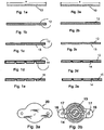
- the base may be of any general heater shape, including a rectangular or round disk shape geometry (as shown in Figure 1A ) with at least a continuous surface.
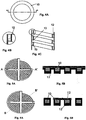
- the solid graphite body may also be of a cylinder shape as shown in Figures 4A - 4C , with an inside diameter, an outside diameter, and a length, and that the wall thickness of the cylinder is machined into a predetermined path, e.g., a serpentine or helical pattern.
- Figure 4A represents a top view of the heater having a cylindrical shape.
- Figure 4B shows the cylindrical heater in cross section taken along the lines A-A of Figure 4A, and
- Figure 4C represents an exploded view of the encircled area shown in Figure 4B .
- the body or base 10 can be of any desired thickness (d) suitable for semiconductor processing applications.
- the thickness of the graphite form may be determined from electrical calculations on the finished part. Fundamental calculations for the finished heater electrical resistance are known in the art, i.e., based on the length, the width, and the thickness of the serpentine electrical path, with the thickness of the electrical path being designed in to the graphite base 10.
- the graphite base 10 may have a thickness of at least 0.05 inches.
- the graphite base 10 may also be in the form of a disk having a thickness of at least about 0.10 inches.
- the graphite base 10 is provided with at least a substantially continuous coating layer 12 of a sufficient thickness to provide the desired corrosion resistance as well as structural integrity and support in the machining step.
- the coating layer 12 may encapsulate both the top and bottom surfaces of the graphite base body 10.
- the coating layer 12 simply covers the top surface of the graphite base body 10 for corrosion resistance and structural support.
- the coating layer may have a thickness of 0.005 to 0.10 inches. This coating layer may also be about 0.01 to 0.05 inches. The coating layer could have a thickness of less than about 0.02 inches.
- the coating layer may be a flat solid substantially continuous surface layer of pBN having a thickness in the range of about .01-.03 inches.
- the coating layer of the graphite body comprises at least one of a nitride, carbide, carbonitride or oxynitride of elements selected from a group consisting of B, Al, Si, Ga, refractory hard metals, transition metals, and rare earth metals, or complexes and / or combinations thereof.
- examples include pyrolytic boron nitride, aluminum nitride, titanium aluminum nitride, titanium nitride, titanium aluminum carbonitride, titanium carbide, silicon carbide, and silicon nitride.
- the coating layer comprises pBN.
- the layer comprises AlN.
- a complex of AlN and BN is a complex of AlN and BN.
- the coating layer comprises a composition of pyrolytic boron nitride (PBN) and a carbon dopant in an amount of less than about 3 wt % such that its electrical resistivity is smaller than 10 14 ⁇ -cm.
- the coating layer comprises an aluminum nitride wherein a small amount of Y 2 O 3 is added, e.g.. in amount of 5 wt % relative to 100 wt % of aluminum nitride.
- Both pBN and AlN have excellent insulating and conducting properties and can be easily deposited from the gaseous phase. They also have a high temperature stability. Additionally, they have a different color (white) than the pyrolytic graphite base (black) such that in the step of forming the electrical patterns, the coating layer can be easily visually distinguished from the patterns.
- the coating layer or layers onto the graphite body substrate can be applied through physical vapor deposition (PVC), wherein the coating material, e.g. boron nitride and / or aluminum nitride is / are transferred in vacuum into the gaseous phase through purely physical methods and are deposited on the surface to be coated.
- PVC physical vapor deposition
- the coating material is deposited onto the surface under high vacuum, wherein it is heated to transition either from the solid via the liquid into the gaseous state or directly from the solid into the gaseous state using electric resistance heating, electron or laser bombardment, electric arc evaporation or the like.
- Sputtering can also be used, wherein a solid target which consists of the respective coating material is atomized in vacuum by high-energy ions, e.g. inert gas ions, in particular argon ions, with the ion source being e.g. an inert gas plasma.
- a target which consists of the respective coating material can also be bombarded with ion beams under vacuum, be transferred into the gaseous phase and be deposited on the surface to be coated.
- the above-mentioned PVD methods can also be combined and at least one of the layers can be deposited e.g. through plasma-supported vapor deposition.
- one of the layers can be deposited through chemical vapor deposition (CVD).
- CVD chemical vapor deposition
- the CVD method has associated chemical reactions.
- the gaseous components produced at temperatures of approximately 200 to 2000° C. through thermal, plasma, photon or laser-activated chemical vapor deposition are transferred with an inert carrier gas, e.g. argon, usually at under-pressure, into a reaction chamber in which the chemical reaction takes place.
- the solid components thereby formed are deposited onto the graphite body to be coated.
- the volatile reaction products are exhausted along with the carrier gas.
- the graphite body 10 is coated with a layer of pyrolytic boron nitride via a CVD process as described in US Patent No. 3,182, 006 .
- a CVD process as described in US Patent No. 3,182, 006 .
- vapors of ammonia and a gaseous boron halide such as boron trichloride (BCl 3 ) in a suitable ratio are used to form a boron nitride deposit on the surface of the graphite base 10.
- At least one of the layers can also be deposited using thermal injection methods, e.g. by means of a plasma injection method.
- a fixed target is heated and transferred into the gaseous phase by means of a plasma burner through application of a high-frequency electromagnetic field and associated ionization of a gas, e.g. air, oxygen, nitrogen, hydrogen, inert gases etc.
- the target may consist, e.g. of boron nitride or aluminum nitride and be transferred into the gaseous phase and deposited on the graphite body to be coated in a purely physical fashion.
- the target can also consist of boron and be deposited as boron nitride on the surface to be coated through reaction with the ionized gas, e.g., nitrogen.
- a thermal spray process is used, i.e., a flame spray technique is used wherein the powder coating feedstock is melted by means of a combustion flame, usually through ignition of gas mixtures of oxygen and another gas.
- a thermal spray process called arc plasma spraying, a DC electric arc creates an ionized gas (a plasma) that is used to spray the molten powdered coating materials in a manner similar to spraying paint.
- the coating material is applied as a paint / spray and sprayed onto the graphite body with an air sprayer.
- the coating material is applied simply as a liquid paint and then dried at sufficiently high temperatures to dry out the coating.
- the BN over-coated graphite structure is dried at a temperature of at least 75°C, and in one embodiment, of at least 100°C to dry out the coating.
- the coated graphite structure is heated to a temperature of at least 500° C. to further bond the nitride coating onto the graphite body.
- the forming of an electrical pattern in the solid graphite body i.e., an electrically isolated, resistive heater path may be done by techniques known in the art, including but not limited to micro machining, micro-brading, laser cutting, chemical etching, or e-beam etching.
- the pattern may be defined for example, by a removable mask or tape.
- Other masking techniques include the use of dissolvable protective coatings, e.g., photoresist. Patterned application allows for controlled heating in localized areas of the graphite body.
- the coated graphite base 10 is machined from the side opposite the substantially continuous coated surface 12 into a desired electrical pattern for resistive heating.
- the pattern 13 is that of a spiral or serpentine configuration as shown in Figure 3B , with open ends adapted for connection to an external power supply.
- the forming of the electrical pattern / the machining operation was conducted through the cross sectional body of the graphite base 10, up to the continuous coated surface 12. As shown, the machining is done without removing the coated layer 12, i.e., the coating is left substantially intact. Also as shown, the prior art machining in Figures 1D and 2D is conducted without going "through" the thickness of the graphite base so that the coated layer 12 remains substantially continuous.
- the machining operation is conducted through the cross sectional body of the graphite base 10, up to the continuous coated surface 12 (and not going through the coating part) for some portions of the graphite base. But in other portions of the graphite base, the coated graphite is machined through.
- Figure 5B is a cross-section view of the heater in Figure A through line A -A'. As shown, the machining is up to the continuous coated surface for the coating layer forming a cross bar, thus maintaining the structural integrity of the heater.
- the remaining portion (not machined through) is in the form of a cross bar as shown in Figures 5A, 5B, 6A and 6B .
- the remaining portion is in the form of a single bar (not shown).
- the remaining portion is in the form of a plurality of parallel or zig zag shaped bars linking the patterned graphite body and providing structural support.
- the patterned graphite body is coated with at least another layer for enhanced corrosion resistance against the wafer processing chemical environment.
- the protective overcoat layer 14 may simply provide a protective layer covering any exposed graphite as illustrated in Figures 2D , 5B and 6B .
- the outer coat may be of the same material, or of a different material from the first coating layer described in the previous sections.
- the outer coat layer covering the patterned graphite body may comprise at least one of a nitride, carbide, carbonitride or oxynitride of elements selected from a group consisting of B, Al, Si, Ga, refractory hard metals, transition metals, and rare earth metals, or complexes and / or combinations thereof.
- the outer coat layer comprises pBN, AlN, SiC, or SiN.
- the overcoat layer 14 can be applied using the same techniques as with the first coating layer 12, or it can be applied using any other techniques known in the art as described in the previous sections, including but not limited to PVD, CVD, powder coating via thermal injection, thermal spraying, arc spraying, painting, and air spraying.
- the overcoat layer has a thickness of 0.005 to 0.20 inches. In another embodiment, from about 0.01 to 0.10 inches. In a third embodiment, the overcoat layer has a thickness of less than about 0.05 inches. In yet a fourth embodiment, the overcoat layer is a flat solid substantially continuous surface layer of pBN having a thickness in the range of about .01-.03 inches.
- the layer thickness is optimized to promote thermal uniformity, taking into advantage the high degree of thermal conductivity anisotropy inherent in pBN.
- multiple overcoat layers are employed, pBN as well as pyrolytic graphite, to promote thermal uniformity.
- electrical contacts 15 are machined through the top coating layer to expose the graphite 10 at contact locations for connection to an external power source.
- electrical contact extensions can be machined into the graphite base 10 at the outset before the final coating process, or added prior to the over coating operation.
- FIGs. 3A and 3B are plan views of a heater element 20 with tabs 16 extended from the coated graphite body, wherein the post connectors may be attached to the heating element 20 through holes 17 of tabs 16.
- the heater of the Invention may be used for different applications particularly semiconductor processing applications as a wafer carrier. It has been found that the mechanical strength of the heater of the present invention to be dramatically improved relative to the strength of a conventional graphite heater.
- the heater in the broad practice of the present invention may be of any suitable size and shape/conformation, as required for the specific use or application envisioned. In one embodiment, it may be of a disk having a dimension of 2" longx2" widex .01" mm thick.
- the electrical pattern as defined by the graphite body may be of various sizes for defining an electrical flow path for at least one zone of an electrical heating circuit.
- the flow path is of a spiral geometrical pattern.
- the surface of the heater of the invention is substantially continuous and coated with overcoat layer or layers without any exposed graphite surfaces for hermetically sealing the patterned heat-generating graphite resistor body, other than those surfaces necessary for electrical connections, thereby preventing short circuits and electrical changes from occurring, and insuring a substantially continuous surface free from graphite dust and particles.
- certain holes or surface features 15 on the top coated surface 14 of the heater for the reason that in most practical wafer processing applications, these features may be required for lifting devices or mounting locations as illustrated in Figures 1E and 2E .
Landscapes
- Resistance Heating (AREA)
- Chemical Vapour Deposition (AREA)
Claims (14)
- Verfahren zum Ausbilden einer Heizvorrichtung, wobei der Prozess die folgenden Schritte umfasst:(a) Versehen eines Graphitkorpus, der aus einem massiven, frei stehenden Korpus konfiguriert ist, mit mindestens einer Oberfläche, die mit einer ersten Deckschicht beschichtet ist, welche mindestens eines von: einem Nitrid, Carbid, Carbonitrid oder Oxynitrid von Elementen gewählt aus einer Gruppe bestehend aus B, Al, Si, Ga, hochschmelzenden Hartmetallen, Übergangsmetallen und Seltenerdmetallen oder Komplexen und/oder Kombinationen derselben umfasst;(b) Konfigurieren eines Musters für einen elektrischen Flussweg, das mindestens eine Zone eines elektrischen Heizkreises in dem in Schritt (a) erhaltenen beschichteten Graphitkorpus festlegt, durch einen Bearbeitungsvorgang, wobei bei einigen Abschnitten des beschichteten Graphitkorpus der Bearbeitungsvorgang durch den Graphitkorpus bis zur ersten Deckschicht, aber nicht durch die erste Deckschicht durchgehend, ausgeführt wird, während in anderen Abschnitten des beschichteten Graphitkorpus der beschichtete Graphitkorpus durchgehend bearbeitet wird;(c) Beschichten des in Schritt (b) erhaltenen mit Muster versehenen Graphitkorpus mit einer zweiten Deckschicht, welche mindestens eines von: einem Nitrid, Carbid, Carbonitrid oder Oxynitrid von Elementen gewählt aus einer Gruppe bestehend aus B, Al, Si, Ga, hochschmelzenden Hartmetallen, Übergangsmetallen und Seltenerdmetallen oder Komplexen und/oder Kombinationen derselben umfasst.
- Verfahren nach Anspruch 1, wobei die Heizvorrichtung spulenförmig ist.
- Verfahren nach Anspruch 2, wobei der in Schritt (a) vorgesehene Graphitkorpus scheibenförmig ist.
- Verfahren nach Anspruch 2 oder 3, wobei für einen Bereich, der eine Querstange über der spulenförmigen Heizvorrichtung bildet, der Bearbeitungsvorgang in Schritt (b) bis zur ersten Deckschicht, aber nicht durch die erste Deckschicht durchgehend, ausgeführt wird.
- Verfahren nach Anspruch 1, wobei für einen Bereich, der eine Stange bildet, der Bearbeitungsvorgang in Schritt (b) bis zu der ersten Deckschicht, aber nicht durch die erste Deckschicht durchgehend, ausgeführt wird.
- Verfahren nach Anspruch 1, wobei für Bereiche, die mehrere parallele oder zickzackförmige Stangen bilden, der Bearbeitungsvorgang in Schritt (b) bis zu der ersten Deckschicht, aber nicht durch die erste Deckschicht durchgehend, ausgeführt wird.
- Verfahren nach Anspruch 1, wobei das Muster des elektrischen Flusswegs Anschlussenden für elektrisch zu verbindende Anschlüsse umfasst, die einen elektrischen Flussweg bilden.
- Verfahren nach Anspruch 1, wobei die erste Deckschicht und die zweite Deckschicht aus dem gleichen Material bestehen, welches mindestens eines von: einem Nitrid, Carbid, Carbonitrid oder Oxynitrid von Elementen gewählt aus einer Gruppe bestehend aus B, Al, Si, Ga, hochschmelzenden Hartmetallen, Übergangsmetallen und Seltenerdmetallen oder Komplexen und/oder Kombinationen derselben umfasst.
- Verfahren nach Anspruch 1, wobei der elektrische Flussweg ein Spiralmuster, ein Serpentinenmuster, ein wendeiförmiges Muster, ein Zickzackmuster, ein durchgehendes Labyrinthmuster, ein spiralförmig gewundenes Muster, ein Wirbelmuster, ein willkürlich verschlungenes Muster oder Kombinationen derselben aufweist.
- Verfahren nach Anspruch 1, wobei die erste Deckschicht und die zweite Deckschicht durch eine Technik gewählt aus einer physikalischen Gasphasenabscheidung, einer chemischen Dampfphasenabscheidung, einem Spritzprozess unter Verwenden eines Luftsprühgeräts, einem eine Walze nutzenden Lackierprozess, einem thermischen Spritzprozess, einem thermischen Spritzprozess, einem thermischen Einspritzprozess und Kombinationen derselben gebildet werden.
- Verfahren nach Anspruch 10, wobei die erste Deckschicht und die zweite Deckschicht mittels chemischer Dampfphasenabscheidung gebildet werden.
- Verfahren nach Anspruch 1, wobei das Muster in dem Graphitkorpus unter Verwenden einer Technik gewählt aus Mikrobearbeitung, Mikroabschleifen, Laserschneiden, chemisches Ätzen und Elektronenstrahlätzen konfiguriert wird.
- Verfahren nach Anspruch 1, wobei der Graphitkorpus eine Scheibe, eine Walze oder ein Zylinder ist.
- Verfahren nach Anspruch 1, welches weiterhin den Schritt des Vorsehens von Anschlussenden für Anschlüsse, die mit dem elektrischen Flussweg elektrisch zu verbinden sind, umfasst.
Applications Claiming Priority (2)
| Application Number | Priority Date | Filing Date | Title |
|---|---|---|---|
| US11/625,329 US7741584B2 (en) | 2007-01-21 | 2007-01-21 | Encapsulated graphite heater and process |
| EP08705624.8A EP2111727B1 (de) | 2007-01-21 | 2008-01-18 | Verkapselter graphitheizer und verfahren |
Related Parent Applications (3)
| Application Number | Title | Priority Date | Filing Date |
|---|---|---|---|
| EP08705624.8 Division | 2008-01-18 | ||
| EP08705624.8A Division EP2111727B1 (de) | 2007-01-21 | 2008-01-18 | Verkapselter graphitheizer und verfahren |
| EP08705624.8A Division-Into EP2111727B1 (de) | 2007-01-21 | 2008-01-18 | Verkapselter graphitheizer und verfahren |
Publications (2)
| Publication Number | Publication Date |
|---|---|
| EP2667685A1 EP2667685A1 (de) | 2013-11-27 |
| EP2667685B1 true EP2667685B1 (de) | 2017-06-14 |
Family
ID=39358069
Family Applications (2)
| Application Number | Title | Priority Date | Filing Date |
|---|---|---|---|
| EP13003431.7A Active EP2667685B1 (de) | 2007-01-21 | 2008-01-18 | Verkapselter Graphitheizer und Verfahren |
| EP08705624.8A Active EP2111727B1 (de) | 2007-01-21 | 2008-01-18 | Verkapselter graphitheizer und verfahren |
Family Applications After (1)
| Application Number | Title | Priority Date | Filing Date |
|---|---|---|---|
| EP08705624.8A Active EP2111727B1 (de) | 2007-01-21 | 2008-01-18 | Verkapselter graphitheizer und verfahren |
Country Status (4)
| Country | Link |
|---|---|
| US (1) | US7741584B2 (de) |
| EP (2) | EP2667685B1 (de) |
| JP (2) | JP2010517224A (de) |
| WO (1) | WO2008088907A2 (de) |
Cited By (1)
| Publication number | Priority date | Publication date | Assignee | Title |
|---|---|---|---|---|
| EP3854754B1 (de) * | 2020-01-21 | 2025-09-24 | Goodrich Corporation | Abgeriebener sammelschienenbereich eines cnt-resistiven elements |
Families Citing this family (19)
| Publication number | Priority date | Publication date | Assignee | Title |
|---|---|---|---|---|
| US20120006809A1 (en) * | 2010-06-23 | 2012-01-12 | Colorado State University Research Foundation | Sublimation crucible with embedded heater element |
| JP5915026B2 (ja) * | 2011-08-26 | 2016-05-11 | 住友大阪セメント株式会社 | 温度測定用板状体及びそれを備えた温度測定装置 |
| JP2013089512A (ja) * | 2011-10-19 | 2013-05-13 | Momentive Performance Materials Inc | ヒータおよびその製造方法 |
| JP2013097943A (ja) * | 2011-10-31 | 2013-05-20 | Momentive Performance Materials Inc | ヒータおよびその製造方法 |
| JP2013118088A (ja) * | 2011-12-02 | 2013-06-13 | Momentive Performance Materials Inc | 円筒形ヒータおよびその製造方法 |
| JP2014002931A (ja) * | 2012-06-19 | 2014-01-09 | Shin Etsu Chem Co Ltd | グラファイトヒーター |
| CN105379415A (zh) * | 2013-07-15 | 2016-03-02 | 莫门蒂夫性能材料股份有限公司 | 带涂层的石墨加热器构造 |
| WO2015077590A1 (en) * | 2013-11-22 | 2015-05-28 | Applied Materials, Inc. | Pad design for electrostatic chuck surface |
| DE102014000313A1 (de) * | 2014-01-10 | 2015-07-16 | Audi Ag | Vorrichtung zum Abgeben eines Duftstoffs und Kraftfahrzeug mit einer derartigen Vorrichtung |
| US10687393B2 (en) * | 2014-06-13 | 2020-06-16 | Momentive Performance Materials Inc. | One-coat encapsulated graphite heater and process |
| US20170051407A1 (en) * | 2015-08-17 | 2017-02-23 | Applied Materials, Inc. | Heating Source For Spatial Atomic Layer Deposition |
| DE102016209012A1 (de) * | 2015-12-18 | 2017-06-22 | E.G.O. Elektro-Gerätebau GmbH | Heizeinrichtung |
| CN108432342B (zh) * | 2015-12-31 | 2022-09-16 | 应用材料公司 | 用于处理腔室的高温加热器 |
| US10237921B2 (en) | 2016-03-18 | 2019-03-19 | Momentive Performance Materials Inc. | Cylindrical heater |
| US10679873B2 (en) * | 2016-09-30 | 2020-06-09 | Ngk Spark Plug Co., Ltd. | Ceramic heater |
| CN110835272A (zh) * | 2019-12-05 | 2020-02-25 | 山东国晶新材料有限公司 | 一种分体式导电陶瓷舟的制备方法 |
| US11665786B2 (en) * | 2019-12-05 | 2023-05-30 | Applied Materials, Inc. | Solid state heater and method of manufacture |
| CN111283334A (zh) * | 2020-03-18 | 2020-06-16 | 常熟通乐电子材料有限公司 | 一种复合加热体的加工工艺 |
| WO2024038475A1 (en) * | 2022-08-16 | 2024-02-22 | M.I.T. S.R.L. | Electrical resistance heating element, more particularly distributed-element resistance and method for realizing such a heating element |
Family Cites Families (23)
| Publication number | Priority date | Publication date | Assignee | Title |
|---|---|---|---|---|
| DE1133719B (de) | 1961-02-21 | 1962-07-26 | Wacker Chemie Gmbh | Verfahren zur Abtrennung von Aceton und anderen Carbonylverbindungen mit 3C-Atomen aus vorgereinigtem Vinylacetat |
| US3717439A (en) * | 1970-11-18 | 1973-02-20 | Tokyo Shibaura Electric Co | Vapour phase reaction apparatus |
| US3636303A (en) * | 1971-03-10 | 1972-01-18 | Gte Sylvania Inc | Apparatus for metal vaporization comprising a reduced cross sectio heater and a refractory vessel |
| US4264803A (en) * | 1978-01-10 | 1981-04-28 | Union Carbide Corporation | Resistance-heated pyrolytic boron nitride coated graphite boat for metal vaporization |
| US4755658A (en) * | 1985-11-12 | 1988-07-05 | Ultra Carbon Corporation | Segmented heater system |
| US5015908A (en) * | 1989-01-23 | 1991-05-14 | Varian Associates, Inc. | Fast warm-up cathode for high power vacuum tubes |
| US5031229A (en) * | 1989-09-13 | 1991-07-09 | Chow Loren A | Deposition heaters |
| EP1120817B8 (de) * | 1991-03-26 | 2007-10-10 | Ngk Insulators, Ltd. | Verwendung eines korrosion beständigen Substratshalters |
| US5343022A (en) | 1992-09-29 | 1994-08-30 | Advanced Ceramics Corporation | Pyrolytic boron nitride heating unit |
| US5444327A (en) * | 1993-06-30 | 1995-08-22 | Varian Associates, Inc. | Anisotropic pyrolytic graphite heater |
| US5459811A (en) * | 1994-02-07 | 1995-10-17 | Mse, Inc. | Metal spray apparatus with a U-shaped electric inlet gas heater and a one-piece electric heater surrounding a nozzle |
| CA2185438C (en) * | 1994-03-16 | 2004-02-10 | Robert Lloyd | Apparatus for eddy current heating, heat storage, electricity generation, and lens moulding process |
| JP3606472B2 (ja) * | 1994-07-12 | 2005-01-05 | 信越化学工業株式会社 | 熱分解窒化ホウ素被覆複層成形体及びその製造方法 |
| CN1047209C (zh) * | 1994-09-28 | 1999-12-08 | 先进陶瓷公司 | 高密度闪蒸器 |
| US5798497A (en) * | 1995-02-02 | 1998-08-25 | Battelle Memorial Institute | Tunable, self-powered integrated arc plasma-melter vitrification system for waste treatment and resource recovery |
| US5830277A (en) * | 1995-05-26 | 1998-11-03 | Mattson Technology, Inc. | Thermal processing system with supplemental resistive heater and shielded optical pyrometry |
| JPH11354260A (ja) * | 1998-06-11 | 1999-12-24 | Shin Etsu Chem Co Ltd | 複層セラミックスヒータ |
| US5977526A (en) * | 1999-03-05 | 1999-11-02 | Board Of Regents The University Of Texas | Heater for high vacuum optical view port |
| US6140624A (en) * | 1999-07-02 | 2000-10-31 | Advanced Ceramics Corporation | Pyrolytic boron nitride radiation heater |
| US6410172B1 (en) | 1999-11-23 | 2002-06-25 | Advanced Ceramics Corporation | Articles coated with aluminum nitride by chemical vapor deposition |
| CN1299322C (zh) * | 2000-11-16 | 2007-02-07 | 麦特逊技术股份有限公司 | 电阻加热一热处理系统用的装置和方法 |
| US6539171B2 (en) * | 2001-01-08 | 2003-03-25 | Watlow Polymer Technologies | Flexible spirally shaped heating element |
| US20040074898A1 (en) * | 2002-10-21 | 2004-04-22 | Mariner John T. | Encapsulated graphite heater and process |
-
2007
- 2007-01-21 US US11/625,329 patent/US7741584B2/en active Active
-
2008
- 2008-01-18 EP EP13003431.7A patent/EP2667685B1/de active Active
- 2008-01-18 EP EP08705624.8A patent/EP2111727B1/de active Active
- 2008-01-18 WO PCT/US2008/000751 patent/WO2008088907A2/en not_active Ceased
- 2008-01-18 JP JP2009546442A patent/JP2010517224A/ja active Pending
-
2013
- 2013-08-12 JP JP2013004672U patent/JP3187417U/ja not_active Expired - Lifetime
Cited By (1)
| Publication number | Priority date | Publication date | Assignee | Title |
|---|---|---|---|---|
| EP3854754B1 (de) * | 2020-01-21 | 2025-09-24 | Goodrich Corporation | Abgeriebener sammelschienenbereich eines cnt-resistiven elements |
Also Published As
| Publication number | Publication date |
|---|---|
| EP2111727A2 (de) | 2009-10-28 |
| WO2008088907A2 (en) | 2008-07-24 |
| JP2010517224A (ja) | 2010-05-20 |
| EP2111727B1 (de) | 2016-04-13 |
| WO2008088907A3 (en) | 2008-12-04 |
| US7741584B2 (en) | 2010-06-22 |
| EP2667685A1 (de) | 2013-11-27 |
| US20080173638A1 (en) | 2008-07-24 |
| JP3187417U (ja) | 2013-11-28 |
Similar Documents
| Publication | Publication Date | Title |
|---|---|---|
| EP2667685B1 (de) | Verkapselter Graphitheizer und Verfahren | |
| US7259358B2 (en) | Encapsulated graphite heater and process | |
| US7364624B2 (en) | Wafer handling apparatus and method of manufacturing thereof | |
| US20160174302A1 (en) | Coated graphite heater configuration | |
| EP0964433B1 (de) | Keramisches Mehrschichtheizelement | |
| US20060096946A1 (en) | Encapsulated wafer processing device and process for making thereof | |
| JP5524213B2 (ja) | 調整可能な電気抵抗率を有するウェーハ処理装置 | |
| CN101026119B (zh) | 耐蚀刻晶片处理装置和其制造方法 | |
| KR102610973B1 (ko) | 정전 척용 매칭된 tcr 줄 히터 설계 | |
| CN109156049B (zh) | 圆柱形加热器 | |
| WO2001013404A1 (en) | Diamond coated parts in a plasma reactor | |
| US10687393B2 (en) | One-coat encapsulated graphite heater and process | |
| US20070241096A1 (en) | Heating element |
Legal Events
| Date | Code | Title | Description |
|---|---|---|---|
| PUAI | Public reference made under article 153(3) epc to a published international application that has entered the european phase |
Free format text: ORIGINAL CODE: 0009012 |
|
| 17P | Request for examination filed |
Effective date: 20130708 |
|
| AC | Divisional application: reference to earlier application |
Ref document number: 2111727 Country of ref document: EP Kind code of ref document: P |
|
| AK | Designated contracting states |
Kind code of ref document: A1 Designated state(s): AT BE BG CH CY CZ DE DK EE ES FI FR GB GR HR HU IE IS IT LI LT LU LV MC MT NL NO PL PT RO SE SI SK TR |
|
| RAP1 | Party data changed (applicant data changed or rights of an application transferred) |
Owner name: MOMENTIVE PERFORMANCE MATERIALS INC. |
|
| 17Q | First examination report despatched |
Effective date: 20160504 |
|
| GRAP | Despatch of communication of intention to grant a patent |
Free format text: ORIGINAL CODE: EPIDOSNIGR1 |
|
| INTG | Intention to grant announced |
Effective date: 20170110 |
|
| GRAS | Grant fee paid |
Free format text: ORIGINAL CODE: EPIDOSNIGR3 |
|
| GRAA | (expected) grant |
Free format text: ORIGINAL CODE: 0009210 |
|
| AC | Divisional application: reference to earlier application |
Ref document number: 2111727 Country of ref document: EP Kind code of ref document: P |
|
| AK | Designated contracting states |
Kind code of ref document: B1 Designated state(s): AT BE BG CH CY CZ DE DK EE ES FI FR GB GR HR HU IE IS IT LI LT LU LV MC MT NL NO PL PT RO SE SI SK TR |
|
| REG | Reference to a national code |
Ref country code: GB Ref legal event code: FG4D |
|
| REG | Reference to a national code |
Ref country code: CH Ref legal event code: EP Ref country code: AT Ref legal event code: REF Ref document number: 902055 Country of ref document: AT Kind code of ref document: T Effective date: 20170615 |
|
| REG | Reference to a national code |
Ref country code: CH Ref legal event code: NV Representative=s name: KELLER AND PARTNER PATENTANWAELTE AG, CH |
|
| REG | Reference to a national code |
Ref country code: IE Ref legal event code: FG4D |
|
| REG | Reference to a national code |
Ref country code: DE Ref legal event code: R096 Ref document number: 602008050725 Country of ref document: DE |
|
| REG | Reference to a national code |
Ref country code: SE Ref legal event code: TRGR |
|
| REG | Reference to a national code |
Ref country code: NL Ref legal event code: FP |
|
| REG | Reference to a national code |
Ref country code: LT Ref legal event code: MG4D |
|
| PG25 | Lapsed in a contracting state [announced via postgrant information from national office to epo] |
Ref country code: NO Free format text: LAPSE BECAUSE OF FAILURE TO SUBMIT A TRANSLATION OF THE DESCRIPTION OR TO PAY THE FEE WITHIN THE PRESCRIBED TIME-LIMIT Effective date: 20170914 Ref country code: GR Free format text: LAPSE BECAUSE OF FAILURE TO SUBMIT A TRANSLATION OF THE DESCRIPTION OR TO PAY THE FEE WITHIN THE PRESCRIBED TIME-LIMIT Effective date: 20170915 Ref country code: FI Free format text: LAPSE BECAUSE OF FAILURE TO SUBMIT A TRANSLATION OF THE DESCRIPTION OR TO PAY THE FEE WITHIN THE PRESCRIBED TIME-LIMIT Effective date: 20170614 Ref country code: LT Free format text: LAPSE BECAUSE OF FAILURE TO SUBMIT A TRANSLATION OF THE DESCRIPTION OR TO PAY THE FEE WITHIN THE PRESCRIBED TIME-LIMIT Effective date: 20170614 Ref country code: HR Free format text: LAPSE BECAUSE OF FAILURE TO SUBMIT A TRANSLATION OF THE DESCRIPTION OR TO PAY THE FEE WITHIN THE PRESCRIBED TIME-LIMIT Effective date: 20170614 |
|
| REG | Reference to a national code |
Ref country code: AT Ref legal event code: MK05 Ref document number: 902055 Country of ref document: AT Kind code of ref document: T Effective date: 20170614 |
|
| PG25 | Lapsed in a contracting state [announced via postgrant information from national office to epo] |
Ref country code: LV Free format text: LAPSE BECAUSE OF FAILURE TO SUBMIT A TRANSLATION OF THE DESCRIPTION OR TO PAY THE FEE WITHIN THE PRESCRIBED TIME-LIMIT Effective date: 20170614 Ref country code: BG Free format text: LAPSE BECAUSE OF FAILURE TO SUBMIT A TRANSLATION OF THE DESCRIPTION OR TO PAY THE FEE WITHIN THE PRESCRIBED TIME-LIMIT Effective date: 20170914 |
|
| REG | Reference to a national code |
Ref country code: FR Ref legal event code: PLFP Year of fee payment: 11 |
|
| PG25 | Lapsed in a contracting state [announced via postgrant information from national office to epo] |
Ref country code: EE Free format text: LAPSE BECAUSE OF FAILURE TO SUBMIT A TRANSLATION OF THE DESCRIPTION OR TO PAY THE FEE WITHIN THE PRESCRIBED TIME-LIMIT Effective date: 20170614 Ref country code: RO Free format text: LAPSE BECAUSE OF FAILURE TO SUBMIT A TRANSLATION OF THE DESCRIPTION OR TO PAY THE FEE WITHIN THE PRESCRIBED TIME-LIMIT Effective date: 20170614 Ref country code: CZ Free format text: LAPSE BECAUSE OF FAILURE TO SUBMIT A TRANSLATION OF THE DESCRIPTION OR TO PAY THE FEE WITHIN THE PRESCRIBED TIME-LIMIT Effective date: 20170614 Ref country code: SK Free format text: LAPSE BECAUSE OF FAILURE TO SUBMIT A TRANSLATION OF THE DESCRIPTION OR TO PAY THE FEE WITHIN THE PRESCRIBED TIME-LIMIT Effective date: 20170614 Ref country code: AT Free format text: LAPSE BECAUSE OF FAILURE TO SUBMIT A TRANSLATION OF THE DESCRIPTION OR TO PAY THE FEE WITHIN THE PRESCRIBED TIME-LIMIT Effective date: 20170614 |
|
| PG25 | Lapsed in a contracting state [announced via postgrant information from national office to epo] |
Ref country code: PL Free format text: LAPSE BECAUSE OF FAILURE TO SUBMIT A TRANSLATION OF THE DESCRIPTION OR TO PAY THE FEE WITHIN THE PRESCRIBED TIME-LIMIT Effective date: 20170614 Ref country code: IS Free format text: LAPSE BECAUSE OF FAILURE TO SUBMIT A TRANSLATION OF THE DESCRIPTION OR TO PAY THE FEE WITHIN THE PRESCRIBED TIME-LIMIT Effective date: 20171014 Ref country code: ES Free format text: LAPSE BECAUSE OF FAILURE TO SUBMIT A TRANSLATION OF THE DESCRIPTION OR TO PAY THE FEE WITHIN THE PRESCRIBED TIME-LIMIT Effective date: 20170614 |
|
| REG | Reference to a national code |
Ref country code: DE Ref legal event code: R097 Ref document number: 602008050725 Country of ref document: DE |
|
| PLBE | No opposition filed within time limit |
Free format text: ORIGINAL CODE: 0009261 |
|
| STAA | Information on the status of an ep patent application or granted ep patent |
Free format text: STATUS: NO OPPOSITION FILED WITHIN TIME LIMIT |
|
| PG25 | Lapsed in a contracting state [announced via postgrant information from national office to epo] |
Ref country code: DK Free format text: LAPSE BECAUSE OF FAILURE TO SUBMIT A TRANSLATION OF THE DESCRIPTION OR TO PAY THE FEE WITHIN THE PRESCRIBED TIME-LIMIT Effective date: 20170614 |
|
| 26N | No opposition filed |
Effective date: 20180315 |
|
| PG25 | Lapsed in a contracting state [announced via postgrant information from national office to epo] |
Ref country code: SI Free format text: LAPSE BECAUSE OF FAILURE TO SUBMIT A TRANSLATION OF THE DESCRIPTION OR TO PAY THE FEE WITHIN THE PRESCRIBED TIME-LIMIT Effective date: 20170614 |
|
| PG25 | Lapsed in a contracting state [announced via postgrant information from national office to epo] |
Ref country code: LU Free format text: LAPSE BECAUSE OF NON-PAYMENT OF DUE FEES Effective date: 20180118 |
|
| REG | Reference to a national code |
Ref country code: IE Ref legal event code: MM4A |
|
| REG | Reference to a national code |
Ref country code: BE Ref legal event code: MM Effective date: 20180131 |
|
| PG25 | Lapsed in a contracting state [announced via postgrant information from national office to epo] |
Ref country code: BE Free format text: LAPSE BECAUSE OF NON-PAYMENT OF DUE FEES Effective date: 20180131 |
|
| PG25 | Lapsed in a contracting state [announced via postgrant information from national office to epo] |
Ref country code: IE Free format text: LAPSE BECAUSE OF NON-PAYMENT OF DUE FEES Effective date: 20180118 |
|
| PG25 | Lapsed in a contracting state [announced via postgrant information from national office to epo] |
Ref country code: MC Free format text: LAPSE BECAUSE OF FAILURE TO SUBMIT A TRANSLATION OF THE DESCRIPTION OR TO PAY THE FEE WITHIN THE PRESCRIBED TIME-LIMIT Effective date: 20170614 |
|
| PG25 | Lapsed in a contracting state [announced via postgrant information from national office to epo] |
Ref country code: MT Free format text: LAPSE BECAUSE OF NON-PAYMENT OF DUE FEES Effective date: 20180118 |
|
| PG25 | Lapsed in a contracting state [announced via postgrant information from national office to epo] |
Ref country code: TR Free format text: LAPSE BECAUSE OF FAILURE TO SUBMIT A TRANSLATION OF THE DESCRIPTION OR TO PAY THE FEE WITHIN THE PRESCRIBED TIME-LIMIT Effective date: 20170614 |
|
| PG25 | Lapsed in a contracting state [announced via postgrant information from national office to epo] |
Ref country code: HU Free format text: LAPSE BECAUSE OF FAILURE TO SUBMIT A TRANSLATION OF THE DESCRIPTION OR TO PAY THE FEE WITHIN THE PRESCRIBED TIME-LIMIT; INVALID AB INITIO Effective date: 20080118 Ref country code: PT Free format text: LAPSE BECAUSE OF FAILURE TO SUBMIT A TRANSLATION OF THE DESCRIPTION OR TO PAY THE FEE WITHIN THE PRESCRIBED TIME-LIMIT Effective date: 20170614 |
|
| PG25 | Lapsed in a contracting state [announced via postgrant information from national office to epo] |
Ref country code: CY Free format text: LAPSE BECAUSE OF FAILURE TO SUBMIT A TRANSLATION OF THE DESCRIPTION OR TO PAY THE FEE WITHIN THE PRESCRIBED TIME-LIMIT Effective date: 20170614 |
|
| REG | Reference to a national code |
Ref country code: CH Ref legal event code: PFA Owner name: MOMENTIVE PERFORMANCE MATERIALS INC., US Free format text: FORMER OWNER: MOMENTIVE PERFORMANCE MATERIALS INC., US |
|
| REG | Reference to a national code |
Ref country code: CH Ref legal event code: U11 Free format text: ST27 STATUS EVENT CODE: U-0-0-U10-U11 (AS PROVIDED BY THE NATIONAL OFFICE) Effective date: 20260201 |
|
| PGFP | Annual fee paid to national office [announced via postgrant information from national office to epo] |
Ref country code: NL Payment date: 20260122 Year of fee payment: 19 |
|
| PGFP | Annual fee paid to national office [announced via postgrant information from national office to epo] |
Ref country code: SE Payment date: 20260126 Year of fee payment: 19 |
|
| PGFP | Annual fee paid to national office [announced via postgrant information from national office to epo] |
Ref country code: GB Payment date: 20260126 Year of fee payment: 19 |
|
| PGFP | Annual fee paid to national office [announced via postgrant information from national office to epo] |
Ref country code: DE Payment date: 20260127 Year of fee payment: 19 |
|
| PGFP | Annual fee paid to national office [announced via postgrant information from national office to epo] |
Ref country code: IT Payment date: 20260123 Year of fee payment: 19 |
|
| PGFP | Annual fee paid to national office [announced via postgrant information from national office to epo] |
Ref country code: FR Payment date: 20260127 Year of fee payment: 19 |
|
| PGFP | Annual fee paid to national office [announced via postgrant information from national office to epo] |
Ref country code: CH Payment date: 20260201 Year of fee payment: 19 |